Datasheet OU T 1A - fscdn.rohm.com
26
〇Product structure : Silicon integrated circuit 〇This product has no designed protection against radioactive rays 1/23 © 2018 ROHM Co., Ltd. All rights reserved. 11.Dec.2018 Rev.001 www.rohm.com TSZ22111 • 14 • 001 TSZ02201-0P2P0C302010-1-2 PS OUT1A OUT1B RNF1 VCC1 OUT2A OUT2B RNF2S GND IN1A IN1B IN2A IN2B VREF1 TEST CR VREF2 GND VCC2 RNF2 RNF1S FAILA Driver IC for PPC Series High Performance, High Reliability 50 V 2ch Brush Motor Drivers for PPC's etc. BD64220EFV General Description BD64220EFV is a built-in 2 channel H bridge motor driver for 2 DC brush motors or 1 bipolar stepping motor. This driver can drive high efficiency by direct PWM or PWM constant current control. There are built in protection circuits in this IC. It is possible to output an abnormal detection signal for Wired-OR that notifies each protection circuit operation, which contributes to set high reliability. Features ■ Single Power Supply Input (Rated voltage of 50 V) ■ Rated Output Current (peak): 2.0 A (2.5 A) ■ Low ON-Resistance DMOS Output ■ Forward, Reverse, Brake, Stop ■ Power Save Function ■ Direct PWM Control ■ PWM Constant Current (the other excitation method) ■ Built-in Spike Noise Cancel Function (External noise filter is unnecessary) ■ Drive 2 DC Brush Motor ■ Drive 1 Stepping Motor ■ FULL STEP, HALF STEP Functionality (Driving Stepping Motor) ■ μSTEP Drive by External DAC (Driving Stepping Motor) ■ Built-in Logic Input Pull-down Resistor ■ Cross-conduction Prevention Circuit ■ Output Abnormal States Detection Signal (Wired-OR) ■ Thermal Shutdown Circuit (TSD) ■ Over-current Protection Circuit (OCP) ■ Under Voltage Lock Out Circuit (UVLO) ■ Over Voltage Lock out Circuit (OVLO) ■ Protects against malfunction when power supply is disconnected (Ghost Supply Prevention function) ■ Adjacent Pins Short Protection ■ Inverted Mounting Protection ■ Micro Miniature, Ultra-thin and High Heat-radiation (exposed metal type) Package Application ■ Plain Paper Copier (PPC), Multi-function Printer, Laser Printer, Inkjet Printer, Photo Printer, FAX, Mini Printer and etc. Key Specifications ■ Range of Power Supply Voltage 8 V to 46.2 V ■ Rated Output Current 2.0 A/Phase ■ Rated Output Current (Peak) 2.5 A/Phase ■ Range of Operating Temperature -25 °C to +85 °C ■ Output ON Resistance 0.65 Ω (Typ) (Total of upper and lower resistors) Package W (Typ) x D (Typ) x H (Max) HTSSOP-B28 9.70 mm x 6.40 mm x 1.00 mm Typical Application Circuit Datasheet
Transcript of Datasheet OU T 1A - fscdn.rohm.com

〇Product structure : Silicon integrated circuit 〇This product has no designed protection against radioactive rays
1/23 © 2018 ROHM Co., Ltd. All rights reserved.
11.Dec.2018 Rev.001
www.rohm.com
TSZ22111 • 14 • 001
TSZ02201-0P2P0C302010-1-2
PS
OUT1A
OUT1B
RNF1
VCC1
OUT2A
OUT2B
RNF2S
GND
IN1A
IN1B
IN2A
IN2B
VREF1
TEST
CR
VREF2
GND
VCC2
RNF2
RNF1S
FAILA
Driver IC for PPC Series High Performance, High Reliability 50 V 2ch Brush Motor Drivers for PPC's etc. BD64220EFV
General Description BD64220EFV is a built-in 2 channel H bridge motor driver for 2 DC brush motors or 1 bipolar stepping motor. This driver can drive high efficiency by direct PWM or PWM constant current control. There are built in protection circuits in this IC. It is possible to output an abnormal detection signal for Wired-OR that notifies each protection circuit operation, which contributes to set high reliability.
Features Single Power Supply Input (Rated voltage of 50 V) Rated Output Current (peak): 2.0 A (2.5 A) Low ON-Resistance DMOS Output Forward, Reverse, Brake, Stop Power Save Function Direct PWM Control PWM Constant Current (the other excitation method) Built-in Spike Noise Cancel Function
(External noise filter is unnecessary) Drive 2 DC Brush Motor Drive 1 Stepping Motor FULL STEP, HALF STEP Functionality (Driving
Stepping Motor) µSTEP Drive by External DAC (Driving Stepping
Motor) Built-in Logic Input Pull-down Resistor Cross-conduction Prevention Circuit Output Abnormal States Detection Signal (Wired-OR) Thermal Shutdown Circuit (TSD) Over-current Protection Circuit (OCP) Under Voltage Lock Out Circuit (UVLO) Over Voltage Lock out Circuit (OVLO) Protects against malfunction when power supply is
disconnected (Ghost Supply Prevention function) Adjacent Pins Short Protection Inverted Mounting Protection Micro Miniature, Ultra-thin and High Heat-radiation
(exposed metal type) Package
Application Plain Paper Copier (PPC), Multi-function Printer,
Laser Printer, Inkjet Printer, Photo Printer, FAX, Mini Printer and etc.
Key Specifications Range of Power Supply Voltage 8 V to 46.2 V Rated Output Current 2.0 A/Phase Rated Output Current (Peak) 2.5 A/Phase Range of Operating Temperature -25 °C to +85 °C Output ON Resistance 0.65 Ω (Typ)
(Total of upper and lower resistors)
Package W (Typ) x D (Typ) x H (Max)
HTSSOP-B28 9.70 mm x 6.40 mm x 1.00 mm
Typical Application Circuit
Datasheet

2/23 © 2018 ROHM Co., Ltd. All rights reserved.
11.Dec.2018 Rev.001
www.rohm.com
TSZ22111 • 15 • 001
BD64220EFV
TSZ02201-0P2P0C302010-1-2
6
5
4
3
2
1
RNF2S
RNF2
RNF1S
NC
OUT1A
RNF1
OUT1B
GND
EXP-PAD
23
24
25
26
27
28
NC
OUT2A
OUT2B
NC
14
13
12
11
VREF2
NC
PS
VREF1
10
9
8
7
NC
CR
GND
VCC1
19
20
21
22
IN2A
IN2B
NC
VCC2
15
16
17
18
FAILA
IN1A
IN1B
TEST
OUT1A
VCC1
OUT1B
RNF1
OUT2A
OUT2B
RNF2
Co
ntr
ol L
og
ic
Pre
drive
r
VCC2
RNF2S
7
5
2
3
22
24
26
27
25
11
OVLOUVLO
OCPTSD
1/8
1/8
Blank time
PWM control
OSCCR 10
12
VREF1
VREF2
RNF1S
RNF2S
Forward
Reverse
Break
Stop
Forward
Reverse
Break
Stop
16
17
19
20
13
18
GND1,9
RNF1S4
IN1A
IN1B
IN2A
IN2B
PS
TEST
FAILA15
Regulator
Pin Configuration
Block Diagram
[TOP VIEW]
Pin Description
1 GND Ground pin 15 FAILA Output signal to detect abnormal states
2 OUT1B H bridge output pin 16 IN1A H bridge control pin
3 RNF1 Connection pin of resistor for output current detection
17 IN1B H bridge control pin
4 RNF1S Input pin of current detection comparator
18 TEST Test pin (Connected to GND)
5 OUT1A H bridge output pin 19 IN2A H bridge control pin
6 NC Non connection 20 IN2B H bridge control pin
7 VCC1 Power supply pin 21 NC Non connection
8 NC Non connection 22 VCC2 Power supply pin
9 GND Ground pin 23 NC Non connection
10 CR Setting chopping frequency 24 OUT2A H bridge output pin
11 VREF1 Output current value setting pin 25 RNF2S Input pin of current detection comparator
12 VREF2 Output current value setting pin 26 RNF2 Connection pin of resistor for output current detection
13 PS Power save pin 27 OUT2B H bridge output pin
14 NC Non connection 28 NC Non connection
- EXP-PAD The EXP-PAD of the product connect to GND.
- - -
Pin No. Pin Name Function Pin No. Pin Name Function

3/23 © 2018 ROHM Co., Ltd. All rights reserved.
11.Dec.2018 Rev.001
www.rohm.com
TSZ22111 • 15 • 001
BD64220EFV
TSZ02201-0P2P0C302010-1-2
Function Explanation PS/ Power Save Pin
The PS pin can make circuit standby state and make motor output OPEN. When PS=L→H, be careful because there is a delay of 40 μs (Max) before it is returned from standby state to normal state and the motor output becomes ACTIVE.
PS Status
L Standby state
H ACTIVE
IN1A, IN1B, IN2A, IN2B/ H bridge Control Pin
This is the pin to decide output pin logic.
Input Output
Status PS
IN1A IN2A
IN1B IN2B
OUT1A OUT2A
OUT1B OUT2B
L X(Note 1) X
(Note 1) OPEN OPEN POWER SAVE (STANDBY)
H L L OPEN OPEN STOP
H H L H L FORWARD
H L H L H REVERSE
H H H L L BREAK (Note 1) x = Low or High
VCC1, VCC2/ Power Supply Pin
Motor’s drive current is flowing in it, so the wire is thick, short and has low impedance. Voltage VCC may have great fluctuation due to counter electromotive force of the motor, PWM switching noise etc. So arrange the bypass capacitor of 100 µF to 470 µF as close to the pin as possible and adjust the voltage VCC is stable. Increase the capacity as needed especially, when a large current is used or those motors that have great back electromotive force are used. In addition, for the purpose of reducing of power supply’s impedance in wideband, it is recommended to set parallel connection of multi-layered ceramic capacitor of 0.01 µF to 0.1 µF etc. Extreme care must be used to make sure that the voltage VCC does not exceed the rating even for a moment. VCC1 and VCC2 are shorted inside IC, but be sure to short externally VCC1 and VCC2 when using. If used without shorting, malfunction or destruction may occur because of concentration of current routes etc. Still more, in the power supply pin, there is built-in clamp component for preventing of electrostatic destruction. When a steep pulse signal or voltage such as a surge the absolute maximum rating or more is applied, this clamp component operates, as a result there is the danger of destruction, so be sure that the absolute maximum rating must not be exceeded. It is effective to mount a Zener diode of about the absolute maximum rating. Moreover, the diode for preventing of electrostatic destruction is inserted between the VCC1, VCC2 and GND pin, as a result there is the danger of IC destruction if reverse voltage is applied between the VCC1, VCC2 and GND pin, so be careful.
GND/ Ground Pin
In order to reduce the noise caused by switching current and to stabilize the internal reference voltage of IC, the wiring impedance from this pin is made as low as possible to achieve the lowest electrical potential no matter what operating state it can be. Moreover, design patterns not to have any common impedance with other GND patterns.
OUT1A, OUT1B, OUT2A, OUT2B/ H Bridge Output Pin Motor’s drive current is flowing in it, so the wire is thick, short and has low impedance. It is also effective to add a Schottky diode if output has positive or negative great fluctuation when large current, for example, counter electromotive voltage etc., is used. Moreover, in the output pin, there is built-in clamp component for preventing of electrostatic destruction. When a steep pulse signal or voltage such as a surge exceeding the absolute maximum rating is applied, this clamp component operates, as a result there is the danger of even destruction, so be sure that the absolute maximum rating must not exceeded.
RNFX
(Note 2)/ Connection Pin of Resistor for Detecting of Output Current Connect the resistor of 0.1 Ω to 0.3 Ω for current detection between this pin and GND. Determine the resistor so that power consumption W=IOUT
2xR [W] of the current-detecting resistor does not exceed rated power consumption. In addition, it has a low impedance and does not have a common impedance with other GND patterns because motor’s drive current flows in the pattern through the RNFX pin to current-detecting resistor to GND. Do not exceed the rating because there is the possibility of circuits’ malfunction etc., if the RNFX voltage has exceeded the maximum rating (0.7 V). Moreover, be careful because if the RNFX pin is shorted to GND, large current flows without normal PWM constant current control, then there is the danger that OCP or TSD will operate. If the RNFX pin is open, then there is the possibility of such malfunction as output current does not flow either, so do not let it open. (Note 2) x = 1 or 2

4/23 © 2018 ROHM Co., Ltd. All rights reserved.
11.Dec.2018 Rev.001
www.rohm.com
TSZ22111 • 15 • 001
BD64220EFV
TSZ02201-0P2P0C302010-1-2
Function Explanation – continued
RNFXS(Note 1)/ Input Pin of Current Limit Comparator In this series, the RNFxS pin, which is the input pin of current detection comparator, is independently arranged in order to decrease the lowering of current-detection accuracy caused by the wire impedance inside the IC of the RNFx(Note 1) pin. Therefore, make sure to connect the RNFx pin and the RNFxS pin together when using PWM constant current control. In addition, in case of interconnection, the lowering of current-detection accuracy caused by the impedance of board pattern between RNFx pin and the current-detecting resistor can be decreased because the wires from the RNFxS pin is connected near the current-detecting resistor. Moreover, design the pattern there is no noise plunging. In addition, be careful because if the RNFxS pin is shorted to GND, large current flows without normal PWM constant current control and, then there is the danger that OCP or TSD will operate. (Note 1) x = 1 or 2
VREFX
(Note 2)/ Output Current Value Setting Pin This is the pin to set the output current value. It can be set by VREFX voltage and current-detecting resistor (RNFX
(Note 2) resistor).
(Note 2) x = 1 or 2
𝐼𝑂𝑈𝑇 =𝑉𝑅𝐸𝐹𝑋
8/ 𝑅𝑁𝐹𝑋 [A]
Where: IOUT is the output current.
VREFX is the voltage of output current value-setting pin.
RNFX is the current-detecting resistor. Avoid using it with the VREFX pin open because if the VREFX pin is open, the input is unsettled, and the VREFX voltage increases, and then there is the possibility of such malfunctions as the setting current increases and a large current flows etc. Keep to the input voltage range because if the voltage of 3 V or more is applied on the VREFX pin, then there is also the danger that a large current flows in the output and so OCP or TSD will operate. Besides, select the resistance value in consideration of the outflow current (Max 2 µA) if it is inputted by resistance division. The minimum current, which can be controlled by VREFX voltage, is determined by motor coil’s L, R values and minimum ON time because there is a minimum ON time in PWM drive.
CR/ Setting Chopping Frequency This is the pin to set the chopping frequency of the output. Connect the external C (1500 pF to 4700 pF) and R (4.7 kΩ to 51 kΩ) between this pin and GND. Refer to P.9, 10. Connect the external components to GND in such a way that the interconnection does not have impedance in common with other GND patterns. In addition, create the pattern design in such a way to keep such sudden pulses as square wave etc. away and that there is few noise spike. Mount the two components of C and R if PWM constant current control is being used. This is because normal PWM constant current control cannot be used if CR pin is open or it is biased externally. When not using PWM constant current control, connect this pin to GND. FAILA/ Output Detection Signal Pin During Abnormal States FAILA outputs abnormal states detect signal (FAILA = L) when Over-Current Protection (OCP) or Thermal Shutdown (TSD) operates. FAILA outputs abnormal states detect signal (FAILA = M) when Thermal Shutdown (TSD) operates only. Even if Under Voltage Lock Out (UVLO) or Over Voltage Lock Out (OVLO) operates, FAILA doesn’t output abnormal states detect signal (FAILA = H). This pin is an open drain type, so set the pull up resistor (5 kΩ to 100 kΩ) to power supply less than 7V (e.g. 5 V or 3.3 V). If not using this pin, connect it to GND.
OCP TSD Output of FAILA Pin
OFF OFF H (OFF)
OFF ON M (ON)
ON OFF L (ON)
ON ON L (ON)
TEST/ Pin for Testing This is the pin used at the time of distribution test. Connect to GND. Be careful because there is a possibility of malfunction if it is not connected to GND.
NC Pin
This pin is unconnected electrically with IC internal circuit.
EXP-PAD For HTSSOP-B28 package, the heat-radiating metal is mounted on IC’s back side, and on the metal the heat-radiating treatment is performed when in use, which becomes the precondition to use, secure sufficiently the heat-radiating area by surely connecting by solder with the GND plane on the board and getting as wide GND pattern as possible. Moreover, the back side metal is shorted with IC chip’s back side and becomes the GND potential, so there is the danger of malfunction and destruction if shorted with potentials other than GND, therefore absolutely do not design patterns other than GND through the IC’s back side.

5/23 © 2018 ROHM Co., Ltd. All rights reserved.
11.Dec.2018 Rev.001
www.rohm.com
TSZ22111 • 15 • 001
BD64220EFV
TSZ02201-0P2P0C302010-1-2
Protection Circuits Thermal Shutdown (TSD)
This IC has a built-in thermal shutdown circuit for thermal protection. When the IC’s chip temperature rises 175 °C (Typ) or more, the motor output becomes OPEN. Also, when the temperature returns to 150 °C (Typ) or less, it automatically returns to normal operation. However, even when TSD is in operation, if heat is continued to be added externally, heat overdrive can lead to destruction.
Over Current Protection (OCP)
This IC has a built-in over current protection circuit as a provision against destruction when the motor outputs are shorted each other or VCC-motor output or motor output-GND is shorted. This circuit latches the motor output to OPEN condition when the regulated current flows for 4 µs (Typ). It returns with power reactivation or a reset by the PS pin. The over current protection circuit’s only aim is to prevent the destruction of the IC from irregular situations such as motor output shorts, and is not meant to be used as protection or security for the set. Therefore, sets should not be designed to take into account this circuit’s functions. After OCP operating, if irregular situations continue and the return by power reactivation or a reset by the PS pin, then OCP operates repeatedly and the IC may generate heat or otherwise deteriorate. When the L value of the wiring is great due to the wiring being long, the motor outputs are shorted each other or VCC-motor output or motor output-GND is shorted., if the output pin voltage jumps up and the absolute maximum values can be exceeded after the over current has flowed, there is a possibility of destruction. Also, when current which is the output current rating or more and the OCP detection current or less flows, the IC can heat up to Tjmax=150 °C exceeds and can deteriorate, so current the output rating or more should not be applied.
Under Voltage Lock Out (UVLO)
This IC has a built-in under voltage lock out function to prevent false operation such as IC output during power supply voltage is low. When the applied voltage to the VCC pin goes 5 V (Typ) or less, the motor output is set to OPEN. This switching voltage has a 1 V (Typ) hysteresis to prevent false operation by noise etc. Be aware that this circuit does not operate during power save mode.
Over Voltage Lock Out (OVLO)
This IC has a built-in over voltage lock out function to protect the IC output and the motor during power supply over voltage. When the applied voltage to the VCC pin goes 51 V (Typ) or more, the motor output is set to OPEN. This switching voltage has a 1 V (Typ) hysteresis and a 4 µs (Typ) mask time to prevent false operation by noise etc. Although this over voltage locked out circuit is built-in, there is a possibility of destruction if the absolute maximum value for power supply voltage is exceeded. Therefore, the absolute maximum value should not be exceeded. Be aware that this circuit does not operate during power save mode.
Protects against malfunction when power supply is disconnected (Ghost Supply Prevention Function)
If a control signal (logic input and VREFX(Note 1)) is input when there is no power supplied to this IC, there is a function which
prevents a malfunction where voltage is supplied to power supply of this IC or other IC in the set via the electrostatic destruction prevention diode from these input pins to the VCC. Therefore, there is no malfunction of the circuit even when voltage is supplied to these control input pins while there is no power supply. (Note 1) x = 1 or 2
Operation Under Strong Electromagnetic Field
The IC is not designed for using in the presence of strong electromagnetic field. Be sure to confirm that no malfunction is found when using the IC in a strong electromagnetic field.

6/23 © 2018 ROHM Co., Ltd. All rights reserved.
11.Dec.2018 Rev.001
www.rohm.com
TSZ22111 • 15 • 001
BD64220EFV
TSZ02201-0P2P0C302010-1-2
Absolute Maximum Rating (Ta=25 °C)
Item Symbol Rated Value Unit
Supply Voltage VCC1, VCC2 -0.2 to +50.0 V
Input Voltage for Control Pin VIN -0.2 to +5.5 V
RNFX(Note 1) Maximum Voltage VRNF 0.7 V
Output Current IOUT 2.0(Note 2) A/Phase
Output Current (peak) (Note 3) IOUTPEAK 2.5 (Note 3) A/Phase
Storage Temperature Range Tstg -55 to +150 °C
Maximum Junction Temperature Tjmax +150 °C
(Note 1) x= 1 or 2
(Note 2) Do not exceed Tjmax = 150 °C.
(Note 3) Pulse width tw ≤1 ms, duty 20 ms
Caution 1: Operating the IC over the absolute maximum ratings may damage the IC. The damage can either be a short circuit between pins or an open circuit between pins and the internal circuitry. Therefore, it is important to consider circuit protection measures, such as adding a fuse, in case the IC is operated over the absolute maximum ratings.
Caution 2: Should by any chance the maximum junction temperature rating be exceeded the rise in temperature of the chip may result in deterioration of the properties of the chip. In case of exceeding this absolute maximum rating, design a PCB with thermal resistance taken into consideration by increasing board size and copper area so as not to exceed the maximum junction temperature rating.
Recommended Operating Condition
Item Symbol Min Typ Max Unit
Supply Voltage VCC1, VCC2 8 37 46.2 V
Operating Temperature Topr -25 +25 +85 °C
Maximum Output Current (DC) IOUT - - 1.4(Note 4) A/Phase
(Note 4) Do not exceed Tjmax = 150 °C.
Thermal Resistance(Note 5)
Parameter Symbol Thermal Resistance (Typ)
Unit 1s(Note 7) 4s(Note 8)
HTSSOP-B28
Junction to Ambient θJA 107.0 25.1 °C/W
Junction to Top Characterization Parameter(Note 6) ΨJT 6 3 °C/W
(Note 5) Based on JESD51-2A(Still-Air). (Note 6) The thermal characterization parameter to report the difference between junction temperature and the temperature at the top center of the outside
surface of the component package. (Note 7) Using a PCB board based on JESD51-3. (Note 8) Using a PCB board based on JESD51-5, 7.
Layer Number of Measurement Board
Material Board Size
Single FR-4 114.3 mm x 76.2 mm x 1.57 mmt
Top
Copper Pattern Thickness
Footprints and Traces 70 μm
Layer Number of Measurement Board
Material Board Size Thermal Via(Note 9)
Pitch Diameter
4 Layers FR-4 114.3 mm x 76.2 mm x 1.6 mmt 1.20 mm Φ0.30 mm
Top 2 Internal Layers Bottom
Copper Pattern Thickness Copper Pattern Thickness Copper Pattern Thickness
Footprints and Traces 70 μm 74.2 mm x 74.2 mm 35 μm 74.2 mm x 74.2 mm 70 μm
(Note 9) This thermal via connects with the copper pattern of all layers.

7/23 © 2018 ROHM Co., Ltd. All rights reserved.
11.Dec.2018 Rev.001
www.rohm.com
TSZ22111 • 15 • 001
BD64220EFV
TSZ02201-0P2P0C302010-1-2
Electrical Characteristics (Unless otherwise specified Ta=25 °C, VCC1=VCC2=37 V)
Item Symbol Specification
Unit Condition Min Typ Max
[Whole]
Circuit Current at Standby ICCST - - 10 µA PS=L
Circuit Current ICC - 2.0 5.0 mA PS=H, VREF1=VREF2=3 V
[Control Input]
H-level Input Voltage VINH 2.0 - - V
L-level Input Voltage VINL - - 0.8 V
H-level Input Current IINH 35 50 100 µA VIN=5 V
L-level Input Current IINL -10 0 - µA VIN=0 V
[Output (OUT1A, OUT1B, OUT2A, OUT2B)]
Output ON Resistance RON - 0.65 0.85 Ω IOUT =±1.0 A
(Sum of upper and lower)
Output Leak Current ILEAK - - 10 µA
[Current Control]
RNFX(Note 1) Input Current IRNF -80 -40 - µA RNFX=0 V
VREFX(Note 1) Input Current IVREF -2.0 -0.1 - µA VREFX=0 V
VREFX(Note 1) Input Voltage Range VVREF 0 - 2.0 V
Comparator Threshold VCTH 0.23 0.25 0.27 V VREFX=2 V
(Note 1) x = 1 or 2

8/23 © 2018 ROHM Co., Ltd. All rights reserved.
11.Dec.2018 Rev.001
www.rohm.com
TSZ22111 • 15 • 001
BD64220EFV
TSZ02201-0P2P0C302010-1-2
M
OFF→ON
ON→OFF OFF→ON
ON→OFF
FAST DECAY
M
OFF→ON
ON→OFF OFF→OFF
ON→ON
SLOW DECAY
When output On
When Current Decay
Direct PWM Control This series can drive by IN1A, IN1B, IN2A, and IN2B input directly PWM control (up to100 kHz) from the microcomputer. Current decay mode can be SLOW DECAY or FAST DECAY. The following diagrams show the state of each transistor, the regenerative current path during the current decay for each decay mode and control sequence example.
SLOW DECAY (forward rotation)
FAST DECAY (synchronous rectification, forward rotation)
Figure 1. Route of Regenerative Current during Current Decay
Input Output
State PS
IN1A IN2A
IN1B IN2B
OUT1A OUT2A
OUT1B OUT2B
H H L H L ON
H H H L L SLOW DECAY
H H L H L ON
H H H L L SLOW DECAY
H H L H L ON
Input Output
State PS
IN1A IN2A
IN1B IN2B
OUT1A OUT2A
OUT1B OUT2B
H H L H L ON
H L H L H FAST DECAY
H H L H L ON
H L H L H FAST DECAY
H H L H L ON

9/23 © 2018 ROHM Co., Ltd. All rights reserved.
11.Dec.2018 Rev.001
www.rohm.com
TSZ22111 • 15 • 001
BD64220EFV
TSZ02201-0P2P0C302010-1-2
PWM Constant Current Control 1 Current control operation
The output current increases due to the output transistor turned on. When the voltage on the RNFX(Note 1) pin, the output
current is converted it due to connect the external resistance to RNFX pin, reaches the voltage value set by the VREFX pin input voltage, the current limit comparator operates and enters current decay mode. Output turns on again after decay time passed by CR timer. The process repeats itself with chopping period (tCHOP). (Note 1) x = 1 or 2
2 Blank Time (Fixed in Internal Circuit)
In order to avoid misdetection of current detection comparator due to RNF spikes that occur when the output turns ON. The IC employs the minimum ON-time (tONMIN), while this time from the output transistor turned on, the current detection is invalid. This allows for constant-current drive without the need for an external filter.
3 CR Timer
The CR pin is repeatedly charged and discharged between the VCRH and VCRL levels by connected the external capacitor and resistor. The CR pin voltage decides in IC and it is VCRL=0.4 V, VCRH=1.0 V respectively. The detection of the current detection comparator is masked while charging from VCRL to VCRH. (As mentioned above, this period defines the minimum ON-time.) The CR pin begins discharging once the voltage reaches VCRH. When the output current reaches the current limit during this period, then the IC enters decay mode. The CR continues to discharge during this period until it reaches VCRL, at which point the IC output is switched back ON. The current output and CR pin begin charging simultaneously. The minimum ON-time (tONMIN) and discharge time (tDISCHARGE) are set by external components, according to the following formulas. The total of tONMIN and tDISCHARGE is the chopping period, tCHOP.
𝑡𝑂𝑁𝑀𝐼𝑁 ≈ 𝐶 ×𝑅′×𝑅
𝑅′+𝑅× 𝑙𝑛 (
𝑉𝐶𝑅−0.4
𝑉𝐶𝑅−1.0) [s]
tONMIN is the minimum ON-time.
C is the external capacitance.
R is the external resistance.
R’ is the CR pin internal impedance 5 kΩ(Typ)
VCR is the CR pin voltage.
𝑉𝐶𝑅 = 𝑉 ×𝑅
𝑅′+𝑅 [V]
V is the internal regulator voltage 5V(Typ).
𝑡𝐷𝐼𝑆𝐶𝐻𝐴𝑅𝐺𝐸 ≈ 𝐶 × 𝑅 × 𝑙𝑛 (1+𝛼
0.4) [s]
tDISCHARGE is the CR discharge time.
α refer to the right graph.
𝑡𝐶𝐻𝑂𝑃 = 𝑡𝑂𝑁𝑀𝐼𝑁 + 𝑡𝐷𝐼𝑆𝐶𝐻𝐴𝑅𝐺𝐸 [s]
tCHOP is the chopping period.
0.00
0.05
0.10
0.15
0.20
0.25
0.30
0 500 1000 1500 2000
α[V
]
C [pF]

10/23 © 2018 ROHM Co., Ltd. All rights reserved.
11.Dec.2018 Rev.001
www.rohm.com
TSZ22111 • 15 • 001
BD64220EFV
TSZ02201-0P2P0C302010-1-2
Output Current
RNFX(Note 1)Voltage
CR Voltage
Current limit value
0mA
GND
Current limit Value
VCRH(1.0V Typ)
GND
Spike noise
Minimum
ON Time
Chopping
PeriodtONMIN tCHOP
VCRL(0.4V Typ)
tDISCHARGE
Discharge time
PWM Constant Current Control – continued
(Note 1) x = 1 or 2
Figure 2. Timing chart of CR voltage, RNF voltage and output current
If this resistance is lower value, CR voltage cannot reach the VCRH voltage level, so 4.7kΩ or more should be connected to the CR pin (4.7 kΩ to 51 kΩ is recommended). A capacitor in the range of 1500 pF to 4700 pF is also recommended. As the capacitance value is several 1000 pF or more, the minimum on time (tONMIN) also increases, and there is a risk that the output current may exceed the current setting value due to the internal L and R components of the output motor coil. Also, ensure that the chopping period (tCHOP) is not set longer than necessary, as doing so will increase the output ripple, thereby decreasing the average output current and the rotation efficiency. Select optimal value so that motor drive sound, and distortion of output current waveform can be minimized.

11/23 © 2018 ROHM Co., Ltd. All rights reserved.
11.Dec.2018 Rev.001
www.rohm.com
TSZ22111 • 15 • 001
BD64220EFV
TSZ02201-0P2P0C302010-1-2
1
23
4
OUT1A
OUT1B
OUT2AOUT2B
FULL STEP
Control Sequence of Stepping Motor
It is possible to drive stepping motor with FULL STEP, HALF STEP, by inputting the following phase switching logic signal. Examples of control sequence and torque vector
Controlled by logic signals of IN1A, IN1B, IN2A, IN2B
Figure 3. FULL STEP Control Sequence
① ② ③ ④
IN1A
IN1B
IN2A
IN2B
IOUT
(CH1)
IOUT
(CH2)
+100%
-100%
+100%
-100%
IN1A IN1B IN2A IN2B OUT1A OUT1B OUT2A OUT2B
① H L H L H L H L
② L H H L L H H L
③ L H L H L H L H
④ H L L H H L L H

12/23 © 2018 ROHM Co., Ltd. All rights reserved.
11.Dec.2018 Rev.001
www.rohm.com
TSZ22111 • 15 • 001
BD64220EFV
TSZ02201-0P2P0C302010-1-2
2
4
OUT1A
OUT1B
OUT2AOUT2B
1
3
5
6
7
8
HALF STEP
Control Sequence of Stepping Motor – continued
Controlled by logic signals of IN1, IN2, IN3, IN4
Figure 4. HALF STEP Control Sequence
① ② ③ ④ ⑤ ⑥ ⑦ ⑧
IN1A
IN1B
IN2A
IN2B
IOUT
(CH1)
IOUT
(CH2)
+100%
-100%
+100%
-100%
IN1A IN1B IN2A IN2B OUT1A OUT1B OUT2A OUT2B
① H L L L H L OPEN OPEN
② H L H L H L H L
③ L L H L OPEN OPEN H L
④ L H H L L H H L
⑤ L H L L L H OPEN OPEN
⑥ L H L H L H L H
⑦ L L L H OPEN OPEN L H
⑧ H L L H H L L H

13/23 © 2018 ROHM Co., Ltd. All rights reserved.
11.Dec.2018 Rev.001
www.rohm.com
TSZ22111 • 15 • 001
BD64220EFV
TSZ02201-0P2P0C302010-1-2
IN1A
IN1BIN2A
IN2B
VREF1
VREF2
IOUT(1ch)
IOUT(2ch)
µ STEP Drive for Stepping Motor Output current of 1ch and 2ch can be determined by VREF1, VREF2. Output logic of 1ch and 2ch can be determined individually by IN1A, IN1B, IN2A, IN2B. Therefore, linear voltage input by external DAC to VREF1, VREF2 and control IN1A, IN1B, IN2A, IN2B, enable to drive stepping motor in µ STEP mode.
Figure 5. Input Signal and Output Current during Driving µSTEP

14/23 © 2018 ROHM Co., Ltd. All rights reserved.
11.Dec.2018 Rev.001
www.rohm.com
TSZ22111 • 15 • 001
BD64220EFV
TSZ02201-0P2P0C302010-1-2
Power Dissipation Confirm that the IC’s chip temperature Tj is not over 150 °C in consideration of the IC’s power consumption (W), thermal resistance (°C/W) and ambient temperature (Ta). When Tj=150 °C is exceeded, the functions as a semiconductor do not operate and problems such as parasitism and leaks occur. Constant use under these circumstances leads to deterioration and eventually destruction of the IC. Tjmax=150 °C must be strictly obeyed under all circumstances.
Thermal Calculation The IC’s consumed power can be estimated roughly with the supply voltage (VCCx
(Note 1)), circuit current (ICC), the upper Pch DMOS ON resistance (RONH) the lower Nch DMOS ON resistance (RONL) and motor output current value (IOUT). The calculation method during direct PWM drive, SLOW DECAY, driving 1ch only is shown here: When using both 1ch and 2ch, calculate for each H bridge. (Note 1) x = 1 or 2
𝑊𝑉𝐶𝐶 = 𝑉𝐶𝐶𝑋 × 𝐼𝐶𝐶 [W]
where: WVCC is the consumed power of the VCC.
VCCX is the supply voltage.
ICC is the circuit current.
𝑊𝐷𝑀𝑂𝑆 = 𝑊𝑂𝑁 + 𝑊𝐷𝐸𝐶𝐴𝑌 [W]
𝑊𝑂𝑁 = (𝑅𝑂𝑁𝐻 + 𝑅𝑂𝑁𝐿) × 𝐼𝑂𝑈𝑇2 × 𝑜𝑛_𝑑𝑢𝑡𝑦 [W]
𝑊𝐷𝐸𝐶𝐴𝑌 = (2 × 𝑅𝑂𝑁𝐿) × 𝐼𝑂𝑈𝑇2 × (1 − 𝑜𝑛_𝑑𝑢𝑡𝑦) [W]
where:
WDMOS is the consumed power of the output DMOS.
WON is the consumed power during output ON.
WDECAY is the consumed power during current decay.
RONH is the upper Pch DMOS ON resistance.
RONL is the lower Nch DMOS ON resistance.
IOUT is the motor output current value.
on_duty PWM on duty
=𝑡𝑂𝑁
𝑡𝐶𝐻𝑂𝑃⁄
tON varies depending on the L and R values of the motor coil and the current set value. Confirm by actual measurement, or make an approximate calculation. tCHOP is the chopping period, which depends on the external CR pin. Refer to P.9 for details.
IC number Upper Pch DMOS ON Resistance
RONH[Ω] (Typ) Lower Nch DMOS ON Resistance
RONL[Ω] (Typ)
BD64220EFV 0.40 0.25
𝑊_𝑡𝑜𝑡𝑎𝑙 = 𝑊𝑉𝐶𝐶 + 𝑊𝐷𝑀𝑂𝑆 [W]
𝑇𝑗 = 𝑇𝑎 + 𝜃𝑗𝑎 × 𝑊_𝑡𝑜𝑡𝑎𝑙 [°C]
where: W_total is the consumed total power of IC.
Tj is the junction temperature.
Ta is the ambient temperature.
θja is the thermal resistance value.
However, the thermal resistance value θja [°C/W] differs greatly depending on circuit board conditions. The calculated values above are only theoretical. For actual thermal design, perform sufficient thermal evaluation for the application board used, and create the thermal design with enough margin not to exceed Tjmax=150 °C. Although unnecessary with normal use, if the IC is used under especially strict heat conditions, consider externally attaching a Schottky diode between the motor output pin and GND to abate heat from the IC.

15/23 © 2018 ROHM Co., Ltd. All rights reserved.
11.Dec.2018 Rev.001
www.rohm.com
TSZ22111 • 15 • 001
BD64220EFV
TSZ02201-0P2P0C302010-1-2
TEST pin
IDIODE
Internal Circuit
VF
-VF[mV]
25 150 Chip Temperature Tj[°C]
Power Dissipation – continued
Temperature Monitoring In respect of BD64220EFV, there is a way to directly measure the approximate chip temperature by using the TEST pin with a protection diode for prevention from electrostatic discharge. However, temperature monitor way is used only for evaluation and experimenting, and must not be used in actual usage conditions.
(1) Measure the pin voltage when a current of IDIODE=50 μA flows from the monitor TEST pin to the GND, without supplying
VCCX(Note 1) to the IC. This measurement is for measuring the VF voltage of the internal diode.
(Note 1) x = 1 or 2
(2) Measure the temperature characteristics of this pin voltage. (VF has a linear negative temperature factor against the
temperature.) With the results of these temperature characteristics, chip temperature can be calibrated from the TEST pin voltage.
(3) Supply VCCX, confirm the TEST pin voltage while running the motor, and the chip temperature can be approximated
from the results of (2).
Figure 6. Model diagram for measuring chip temperature
16/23 © 2018 ROHM Co., Ltd. All rights reserved.
11.Dec.2018 Rev.001
www.rohm.com
TSZ22111 • 15 • 001
BD64220EFV
TSZ02201-0P2P0C302010-1-2
OUT1A
VCC1
OUT1B
RNF1
OUT2A
OUT2B
RNF2
Co
ntr
ol L
og
ic
Pre
drive
r
VCC2
RNF2S
7
5
2
22
24
26
27
25
OVLOUVLO
OCPTSD
1/8
1/8
Blank time
PWM control
OSCCR 10
VREF1
VREF2
RNF1S
RNF2S
Forward
Reverse
Break
Stop
Forward
Reverse
Break
Stop
16
17
19
20
13
18GND
1,9
RNF1S4
IN1A
IN1B
IN2A
IN2B
PS
TEST
FAILA15
Regulator
3 0.1 µF 100 µF
M
M
10kΩ
3.3V or 5.0V
12
11
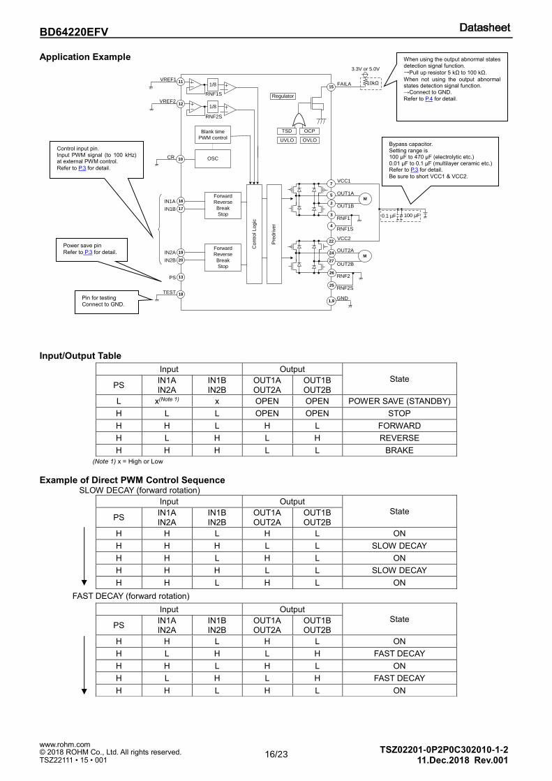
Application Example
Input/Output Table
(Note 1) x = High or Low
Example of Direct PWM Control Sequence SLOW DECAY (forward rotation)
FAST DECAY (forward rotation)
Input Output
State PS
IN1A IN2A
IN1B IN2B
OUT1A OUT2A
OUT1B OUT2B
L x(Note 1) x OPEN OPEN POWER SAVE (STANDBY)
H L L OPEN OPEN STOP
H H L H L FORWARD
H L H L H REVERSE
H H H L L BRAKE
Input Output
State PS
IN1A IN2A
IN1B IN2B
OUT1A OUT2A
OUT1B OUT2B
H H L H L ON
H H H L L SLOW DECAY
H H L H L ON
H H H L L SLOW DECAY
H H L H L ON
Input Output
State PS
IN1A IN2A
IN1B IN2B
OUT1A OUT2A
OUT1B OUT2B
H H L H L ON
H L H L H FAST DECAY
H H L H L ON
H L H L H FAST DECAY
H H L H L ON
Control input pin. Input PWM signal (to 100 kHz) at external PWM control.
Refer to P.3 for detail.
Power save pin
Refer to P.3 for detail.
Pin for testing Connect to GND.
When using the output abnormal states detection signal function.
→Pull up resistor 5 kΩ to 100 kΩ.
When not using the output abnormal states detection signal function. →Connect to GND.
Refer to P.4 for detail.
Bypass capacitor. Setting range is 100 µF to 470 µF (electrolytic etc.) 0.01 µF to 0.1 µF (multilayer ceramic etc.) Refer to P.3 for detail.
Be sure to short VCC1 & VCC2.

17/23 © 2018 ROHM Co., Ltd. All rights reserved.
11.Dec.2018 Rev.001
www.rohm.com
TSZ22111 • 15 • 001
BD64220EFV
TSZ02201-0P2P0C302010-1-2
0.2Ω
0.2Ω
3300pF10kΩ
4.7kΩ
1.2kΩ
4.7kΩ
4.7kΩ
OUT1A
VCC1
OUT1B
RNF1
OUT2A
OUT2B
RNF2
Co
ntr
ol L
og
ic
Pre
drive
r
VCC2
RNF2S
7
5
2
22
24
26
27
25
OVLOUVLO
OCPTSD
1/8
1/8
Blank time
PWM control
OSCCR 10
12
VREF1
VREF2
RNF1S
RNF2S
Forward
Reverse
Break
Stop
Forward
Reverse
Break
Stop
16
17
19
20
13
18GND
1,9
RNF1S4
IN1A
IN1B
IN2A
IN2B
PS
TEST
FAILA15
Regulator
11
3 0.1 µF 100 µF
M
M
10kΩ
3.3V or 5.0V
3.3V or 5.0V
3.3V or 5.0V
PWM Constant Current Control
Input/ Output Table
(Note 1) x = High or Low
Input Output
State PS
IN1A IN2A
IN1B IN2B
OUT1A OUT2A
OUT1B OUT2B
L x(Note 1) x OPEN OPEN POWER SAVE (STANDBY)
H L L OPEN OPEN STOP
H H L H L FORWARD
H L H L H REVERSE
H H H L L BRAKE
Sets the current limit value. Input range: 0 V to 2 V Refer to P.4 for detail.
Sets the PWM frequency. Setting range is C:1500 pF to 4700 pF R:4.7 kΩ to 51 kΩ
Refer to P.4 for detail.
Control logic input pin.
Refer to P.3 for detail.
Power save pin
Refer to P.3 for detail.
Pin for testing
Connect to GND.
When using the output abnormal states detection signal function. →Pull up resistor 5 kΩ to 100 kΩ. When using the output abnormal states detection signal function. →Connect to GND.
Refer to P.4 for detail.
Bypass capacitor. Setting range is
100 µF to 470 µF (electrolytic etc.)
0.01 µF to 0.1 µF (multilayer ceramic etc.) Refer to P.3 for detail.
Be sure to short VCC1 & VCC2.
Current detection setting resistor. 0.1 Ω to 0.3 Ω Refer to P.3, 4 for detail.
Current detection setting resistor 0.1 Ω to 0.3 Ω
Refer to P.3. 4 for detail.

18/23 © 2018 ROHM Co., Ltd. All rights reserved.
11.Dec.2018 Rev.001
www.rohm.com
TSZ22111 • 15 • 001
BD64220EFV
TSZ02201-0P2P0C302010-1-2
100kΩ
10kΩ
PS
IN1A
IN1B
IN2A
IN2B
5kΩ RNF2SRNF1S
Circuitry
OUT2B
VCC1, VCC2
OUT1BOUT2AOUT1A
RNF1RNF2
VREG(internal regulator)
CR
5kΩ
5kΩ
5kΩ VREF2VREF1
10kΩ
I/O Equivalence Circuit
FAILA5kΩ
19/23 © 2018 ROHM Co., Ltd. All rights reserved.
11.Dec.2018 Rev.001
www.rohm.com
TSZ22111 • 15 • 001
BD64220EFV
TSZ02201-0P2P0C302010-1-2
Operational Notes
1. Reverse Connection of Power Supply
Connecting the power supply in reverse polarity can damage the IC. Take precautions against reverse polarity when connecting the power supply, such as mounting an external diode between the power supply and the IC’s power supply pins.
2. Power Supply Lines
Design the PCB layout pattern to provide low impedance supply lines. Furthermore, connect a capacitor to ground at all power supply pins. Consider the effect of temperature and aging on the capacitance value when using electrolytic capacitors.
3. Ground Voltage
Ensure that no pins are at a voltage below that of the ground pin at any time, even during transient condition.
4. Ground Wiring Pattern
When using both small-signal and large-current ground traces, the two ground traces should be routed separately but connected to a single ground at the reference point of the application board to avoid fluctuations in the small-signal ground caused by large currents. Also ensure that the ground traces of external components do not cause variations on the ground voltage. The ground lines must be as short and thick as possible to reduce line impedance.
5. Recommended Operating Conditions
The function and operation of the IC are guaranteed within the range specified by the recommended operating conditions. The characteristic values are guaranteed only under the conditions of each item specified by the electrical characteristics.
6. Inrush Current
When power is first supplied to the IC, it is possible that the internal logic may be unstable and inrush current may flow instantaneously due to the internal powering sequence and delays, especially if the IC has more than one power supply. Therefore, give special consideration to power coupling capacitance, power wiring, width of ground wiring, and routing of connections.
7. Testing on Application Boards
When testing the IC on an application board, connecting a capacitor directly to a low-impedance output pin may subject the IC to stress. Always discharge capacitors completely after each process or step. The IC’s power supply should always be turned off completely before connecting or removing it from the test setup during the inspection process. To prevent damage from static discharge, ground the IC during assembly and use similar precautions during transport and storage.
8. Inter-pin Short and Mounting Errors
Ensure that the direction and position are correct when mounting the IC on the PCB. Incorrect mounting may result in damaging the IC. Avoid nearby pins being shorted to each other especially to ground, power supply and output pin. Inter-pin shorts could be due to many reasons such as metal particles, water droplets (in very humid environment) and unintentional solder bridge deposited in between pins during assembly to name a few.
9. Unused Input Pins
Input pins of an IC are often connected to the gate of a MOS transistor. The gate has extremely high impedance and extremely low capacitance. If left unconnected, the electric field from the outside can easily charge it. The small charge acquired in this way is enough to produce a significant effect on the conduction through the transistor and cause unexpected operation of the IC. So unless otherwise specified, unused input pins should be connected to the power supply or ground line.
20/23 © 2018 ROHM Co., Ltd. All rights reserved.
11.Dec.2018 Rev.001
www.rohm.com
TSZ22111 • 15 • 001
BD64220EFV
TSZ02201-0P2P0C302010-1-2
Operational Notes – continued
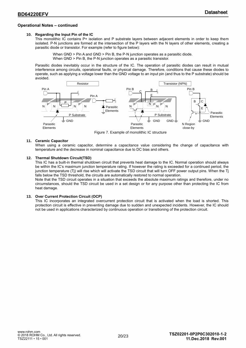
10. Regarding the Input Pin of the IC
This monolithic IC contains P+ isolation and P substrate layers between adjacent elements in order to keep them isolated. P-N junctions are formed at the intersection of the P layers with the N layers of other elements, creating a parasitic diode or transistor. For example (refer to figure below):
When GND > Pin A and GND > Pin B, the P-N junction operates as a parasitic diode. When GND > Pin B, the P-N junction operates as a parasitic transistor.
Parasitic diodes inevitably occur in the structure of the IC. The operation of parasitic diodes can result in mutual interference among circuits, operational faults, or physical damage. Therefore, conditions that cause these diodes to operate, such as applying a voltage lower than the GND voltage to an input pin (and thus to the P substrate) should be avoided.
Figure 7. Example of monolithic IC structure
11. Ceramic Capacitor
When using a ceramic capacitor, determine a capacitance value considering the change of capacitance with temperature and the decrease in nominal capacitance due to DC bias and others.
12. Thermal Shutdown Circuit(TSD)
This IC has a built-in thermal shutdown circuit that prevents heat damage to the IC. Normal operation should always be within the IC’s maximum junction temperature rating. If however the rating is exceeded for a continued period, the junction temperature (Tj) will rise which will activate the TSD circuit that will turn OFF power output pins. When the Tj falls below the TSD threshold, the circuits are automatically restored to normal operation. Note that the TSD circuit operates in a situation that exceeds the absolute maximum ratings and therefore, under no circumstances, should the TSD circuit be used in a set design or for any purpose other than protecting the IC from heat damage.
13. Over Current Protection Circuit (OCP)
This IC incorporates an integrated overcurrent protection circuit that is activated when the load is shorted. This protection circuit is effective in preventing damage due to sudden and unexpected incidents. However, the IC should not be used in applications characterized by continuous operation or transitioning of the protection circuit.
N NP
+ P
N NP
+
P Substrate
GND
NP
+
N NP
+N P
P Substrate
GND GND
Parasitic
Elements
Pin A
Pin A
Pin B Pin B
B C
E
Parasitic
Elements
GNDParasitic
Elements
CB
E
Transistor (NPN)Resistor
N Region
close-by
Parasitic
Elements

21/23 © 2018 ROHM Co., Ltd. All rights reserved.
11.Dec.2018 Rev.001
www.rohm.com
TSZ22111 • 15 • 001
BD64220EFV
TSZ02201-0P2P0C302010-1-2
Ordering Information
B D 6 4 2 2 0 E F V - E 2
ROHM Model Package type EFV: HTSSOP-B28
Packing, Forming specification E2: Reel-wound embossed taping
Marking Diagram
HTSSOP-B28 (TOP VIEW)
BD64220EFV
Part Number Marking
LOT Number
Pin 1 Mark

22/23 © 2018 ROHM Co., Ltd. All rights reserved.
11.Dec.2018 Rev.001
www.rohm.com
TSZ22111 • 15 • 001
BD64220EFV
TSZ02201-0P2P0C302010-1-2
Physical Dimension and Packing Information
Package Name HTSSOP-B28

23/23 © 2018 ROHM Co., Ltd. All rights reserved.
11.Dec.2018 Rev.001
www.rohm.com
TSZ22111 • 15 • 001
BD64220EFV
TSZ02201-0P2P0C302010-1-2
Revision History
Date Revision Changes
11.Dec.2018 001 New Release
Notice-PGA-E Rev.004
© 2015 ROHM Co., Ltd. All rights reserved.
Notice
Precaution on using ROHM Products 1. Our Products are designed and manufactured for application in ordinary electronic equipment (such as AV equipment,
OA equipment, telecommunication equipment, home electronic appliances, amusement equipment, etc.). If youintend to use our Products in devices requiring extremely high reliability (such as medical equipment (Note 1), transportequipment, traffic equipment, aircraft/spacecraft, nuclear power controllers, fuel controllers, car equipment including caraccessories, safety devices, etc.) and whose malfunction or failure may cause loss of human life, bodily injury orserious damage to property (“Specific Applications”), please consult with the ROHM sales representative in advance.Unless otherwise agreed in writing by ROHM in advance, ROHM shall not be in any way responsible or liable for anydamages, expenses or losses incurred by you or third parties arising from the use of any ROHM’s Products for SpecificApplications.
(Note1) Medical Equipment Classification of the Specific Applications
JAPAN USA EU CHINA
CLASSⅢ CLASSⅢ
CLASSⅡb CLASSⅢ
CLASSⅣ CLASSⅢ
2. ROHM designs and manufactures its Products subject to strict quality control system. However, semiconductorproducts can fail or malfunction at a certain rate. Please be sure to implement, at your own responsibilities, adequatesafety measures including but not limited to fail-safe design against the physical injury, damage to any property, whicha failure or malfunction of our Products may cause. The following are examples of safety measures:
[a] Installation of protection circuits or other protective devices to improve system safety [b] Installation of redundant circuits to reduce the impact of single or multiple circuit failure
3. Our Products are designed and manufactured for use under standard conditions and not under any special orextraordinary environments or conditions, as exemplified below. Accordingly, ROHM shall not be in any wayresponsible or liable for any damages, expenses or losses arising from the use of any ROHM’s Products under anyspecial or extraordinary environments or conditions. If you intend to use our Products under any special orextraordinary environments or conditions (as exemplified below), your independent verification and confirmation ofproduct performance, reliability, etc, prior to use, must be necessary:
[a] Use of our Products in any types of liquid, including water, oils, chemicals, and organic solvents [b] Use of our Products outdoors or in places where the Products are exposed to direct sunlight or dust [c] Use of our Products in places where the Products are exposed to sea wind or corrosive gases, including Cl2,
H2S, NH3, SO2, and NO2
[d] Use of our Products in places where the Products are exposed to static electricity or electromagnetic waves [e] Use of our Products in proximity to heat-producing components, plastic cords, or other flammable items [f] Sealing or coating our Products with resin or other coating materials [g] Use of our Products without cleaning residue of flux (Exclude cases where no-clean type fluxes is used.
However, recommend sufficiently about the residue.) ; or Washing our Products by using water or water-soluble cleaning agents for cleaning residue after soldering
[h] Use of the Products in places subject to dew condensation
4. The Products are not subject to radiation-proof design.
5. Please verify and confirm characteristics of the final or mounted products in using the Products.
6. In particular, if a transient load (a large amount of load applied in a short period of time, such as pulse, is applied, confirmation of performance characteristics after on-board mounting is strongly recommended. Avoid applying power exceeding normal rated power; exceeding the power rating under steady-state loading condition may negatively affect product performance and reliability.
7. De-rate Power Dissipation depending on ambient temperature. When used in sealed area, confirm that it is the use inthe range that does not exceed the maximum junction temperature.
8. Confirm that operation temperature is within the specified range described in the product specification.
9. ROHM shall not be in any way responsible or liable for failure induced under deviant condition from what is defined inthis document.
Precaution for Mounting / Circuit board design 1. When a highly active halogenous (chlorine, bromine, etc.) flux is used, the residue of flux may negatively affect product
performance and reliability.
2. In principle, the reflow soldering method must be used on a surface-mount products, the flow soldering method mustbe used on a through hole mount products. If the flow soldering method is preferred on a surface-mount products,please consult with the ROHM representative in advance.
For details, please refer to ROHM Mounting specification

Notice-PGA-E Rev.004
© 2015 ROHM Co., Ltd. All rights reserved.
Precautions Regarding Application Examples and External Circuits 1. If change is made to the constant of an external circuit, please allow a sufficient margin considering variations of the
characteristics of the Products and external components, including transient characteristics, as well as static characteristics.
2. You agree that application notes, reference designs, and associated data and information contained in this document
are presented only as guidance for Products use. Therefore, in case you use such information, you are solely responsible for it and you must exercise your own independent verification and judgment in the use of such information contained in this document. ROHM shall not be in any way responsible or liable for any damages, expenses or losses incurred by you or third parties arising from the use of such information.
Precaution for Electrostatic This Product is electrostatic sensitive product, which may be damaged due to electrostatic discharge. Please take proper caution in your manufacturing process and storage so that voltage exceeding the Products maximum rating will not be applied to Products. Please take special care under dry condition (e.g. Grounding of human body / equipment / solder iron, isolation from charged objects, setting of Ionizer, friction prevention and temperature / humidity control).
Precaution for Storage / Transportation 1. Product performance and soldered connections may deteriorate if the Products are stored in the places where:
[a] the Products are exposed to sea winds or corrosive gases, including Cl2, H2S, NH3, SO2, and NO2 [b] the temperature or humidity exceeds those recommended by ROHM [c] the Products are exposed to direct sunshine or condensation [d] the Products are exposed to high Electrostatic
2. Even under ROHM recommended storage condition, solderability of products out of recommended storage time period may be degraded. It is strongly recommended to confirm solderability before using Products of which storage time is exceeding the recommended storage time period.
3. Store / transport cartons in the correct direction, which is indicated on a carton with a symbol. Otherwise bent leads
may occur due to excessive stress applied when dropping of a carton. 4. Use Products within the specified time after opening a humidity barrier bag. Baking is required before using Products of
which storage time is exceeding the recommended storage time period.
Precaution for Product Label A two-dimensional barcode printed on ROHM Products label is for ROHM’s internal use only.
Precaution for Disposition When disposing Products please dispose them properly using an authorized industry waste company.
Precaution for Foreign Exchange and Foreign Trade act Since concerned goods might be fallen under listed items of export control prescribed by Foreign exchange and Foreign trade act, please consult with ROHM in case of export.
Precaution Regarding Intellectual Property Rights 1. All information and data including but not limited to application example contained in this document is for reference
only. ROHM does not warrant that foregoing information or data will not infringe any intellectual property rights or any other rights of any third party regarding such information or data.
2. ROHM shall not have any obligations where the claims, actions or demands arising from the combination of the Products with other articles such as components, circuits, systems or external equipment (including software).
3. No license, expressly or implied, is granted hereby under any intellectual property rights or other rights of ROHM or any third parties with respect to the Products or the information contained in this document. Provided, however, that ROHM will not assert its intellectual property rights or other rights against you or your customers to the extent necessary to manufacture or sell products containing the Products, subject to the terms and conditions herein.
Other Precaution 1. This document may not be reprinted or reproduced, in whole or in part, without prior written consent of ROHM.
2. The Products may not be disassembled, converted, modified, reproduced or otherwise changed without prior written consent of ROHM.
3. In no event shall you use in any way whatsoever the Products and the related technical information contained in the Products or this document for any military purposes, including but not limited to, the development of mass-destruction weapons.
4. The proper names of companies or products described in this document are trademarks or registered trademarks of ROHM, its affiliated companies or third parties.

DatasheetDatasheet
Notice – WE Rev.001© 2015 ROHM Co., Ltd. All rights reserved.
General Precaution 1. Before you use our Products, you are requested to carefully read this document and fully understand its contents.
ROHM shall not be in any way responsible or liable for failure, malfunction or accident arising from the use of any ROHM’s Products against warning, caution or note contained in this document.
2. All information contained in this document is current as of the issuing date and subject to change without any prior
notice. Before purchasing or using ROHM’s Products, please confirm the latest information with a ROHM sales representative.
3. The information contained in this document is provided on an “as is” basis and ROHM does not warrant that all
information contained in this document is accurate and/or error-free. ROHM shall not be in any way responsible or liable for any damages, expenses or losses incurred by you or third parties resulting from inaccuracy or errors of or concerning such information.