
Datasheet - chipcraft-ic.comchipcraft-ic.com/download/CC-UART-APB.pdf · CC-UART-APB Documentation...
37
Datasheet CC-UART-APB Documentation 1.1 Scope This document describes the CC-UART-APB IP core. Module features and configuration registers are described. The document contains integration guide that covers synthesis options and instantiation example for easy implementation in customer’s environment.
Transcript of Datasheet - chipcraft-ic.comchipcraft-ic.com/download/CC-UART-APB.pdf · CC-UART-APB Documentation...

Datasheet
CC-UART-APB Documentation
1.1
Scope
This document describes the CC-UART-APB IP core. Module features and
configuration registers are described. The document contains integration
guide that covers synthesis options and instantiation example for easy
implementation in customer’s environment.

Contents
1. UART Controller . . . . . . . . . . . . . . . . . . . . . . . . . . . . . . . . . . . . . . . . . . . . . . . . . . . . . . . . . 4
1.1 Functionality . . . . . . . . . . . . . . . . . . . . . . . . . . . . . . . . . . . . . . . . . . . . . . . . . . . . . . . . 4
1.2 Overview . . . . . . . . . . . . . . . . . . . . . . . . . . . . . . . . . . . . . . . . . . . . . . . . . . . . . . . . . . 5
1.3 Data Frame . . . . . . . . . . . . . . . . . . . . . . . . . . . . . . . . . . . . . . . . . . . . . . . . . . . . . . . . . 6
1.4 Data Sampling . . . . . . . . . . . . . . . . . . . . . . . . . . . . . . . . . . . . . . . . . . . . . . . . . . . . . . . 7
1.5 Transmitter Module . . . . . . . . . . . . . . . . . . . . . . . . . . . . . . . . . . . . . . . . . . . . . . . . . . . . . 8
1.5.1 Data Transmission . . . . . . . . . . . . . . . . . . . . . . . . . . . . . . . . . . . . . . . . . . . . . . . . . 9
1.5.2 Break Frame Transmission . . . . . . . . . . . . . . . . . . . . . . . . . . . . . . . . . . . . . . . . . . . . 9
1.5.3 RS485 Mode . . . . . . . . . . . . . . . . . . . . . . . . . . . . . . . . . . . . . . . . . . . . . . . . . . . . 10
1.6 Data Reception . . . . . . . . . . . . . . . . . . . . . . . . . . . . . . . . . . . . . . . . . . . . . . . . . . . . . . . 11
1.6.1 Frame Reception . . . . . . . . . . . . . . . . . . . . . . . . . . . . . . . . . . . . . . . . . . . . . . . . . 11
1.6.2 Start Bit Detection . . . . . . . . . . . . . . . . . . . . . . . . . . . . . . . . . . . . . . . . . . . . . . . . . 11
1.6.3 Data Bits Detection . . . . . . . . . . . . . . . . . . . . . . . . . . . . . . . . . . . . . . . . . . . . . . . . 12
1.6.4 Stop Bit Detection . . . . . . . . . . . . . . . . . . . . . . . . . . . . . . . . . . . . . . . . . . . . . . . . . 12
1.6.5 Receiver Error Flags . . . . . . . . . . . . . . . . . . . . . . . . . . . . . . . . . . . . . . . . . . . . . . . 13
1.7 Hardware Flow Control . . . . . . . . . . . . . . . . . . . . . . . . . . . . . . . . . . . . . . . . . . . . . . . . . . 14
1.7.1 RTS Line . . . . . . . . . . . . . . . . . . . . . . . . . . . . . . . . . . . . . . . . . . . . . . . . . . . . . . 14
1.7.2 CTS Line . . . . . . . . . . . . . . . . . . . . . . . . . . . . . . . . . . . . . . . . . . . . . . . . . . . . . . 15
1.7.3 Pad Output Enable . . . . . . . . . . . . . . . . . . . . . . . . . . . . . . . . . . . . . . . . . . . . . . . . 15
1.8 Interrupts . . . . . . . . . . . . . . . . . . . . . . . . . . . . . . . . . . . . . . . . . . . . . . . . . . . . . . . . . . 16
1.8.1 TXC Interrupt . . . . . . . . . . . . . . . . . . . . . . . . . . . . . . . . . . . . . . . . . . . . . . . . . . . 16
1.8.2 RXC Interrupt . . . . . . . . . . . . . . . . . . . . . . . . . . . . . . . . . . . . . . . . . . . . . . . . . . . 16
1.8.3 TXDRE Interrupt . . . . . . . . . . . . . . . . . . . . . . . . . . . . . . . . . . . . . . . . . . . . . . . . . . 16
1.8.4 Parity Error Interrupt . . . . . . . . . . . . . . . . . . . . . . . . . . . . . . . . . . . . . . . . . . . . . . . . 16
1.8.5 Framing Error Interrupt . . . . . . . . . . . . . . . . . . . . . . . . . . . . . . . . . . . . . . . . . . . . . . 16
1.8.6 Overrun Error Interrupt . . . . . . . . . . . . . . . . . . . . . . . . . . . . . . . . . . . . . . . . . . . . . . 17
1.8.7 Break Reception Started Interrupt . . . . . . . . . . . . . . . . . . . . . . . . . . . . . . . . . . . . . . . . 17
1.8.8 Break Reception Ended Interrupt . . . . . . . . . . . . . . . . . . . . . . . . . . . . . . . . . . . . . . . . . 17
1.8.9 CTS Rising Interrupt . . . . . . . . . . . . . . . . . . . . . . . . . . . . . . . . . . . . . . . . . . . . . . . 17
1.9 Configuration Registers . . . . . . . . . . . . . . . . . . . . . . . . . . . . . . . . . . . . . . . . . . . . . . . . . . 18
1.9.1 Registers List . . . . . . . . . . . . . . . . . . . . . . . . . . . . . . . . . . . . . . . . . . . . . . . . . . . 18
1.9.2 Status Register . . . . . . . . . . . . . . . . . . . . . . . . . . . . . . . . . . . . . . . . . . . . . . . . . . 18
1.9.3 Prescaler Register . . . . . . . . . . . . . . . . . . . . . . . . . . . . . . . . . . . . . . . . . . . . . . . . . 20
1.9.4 Control Register . . . . . . . . . . . . . . . . . . . . . . . . . . . . . . . . . . . . . . . . . . . . . . . . . . 21
1.9.5 Mode Register . . . . . . . . . . . . . . . . . . . . . . . . . . . . . . . . . . . . . . . . . . . . . . . . . . . 22
1.9.6 Transmit Data Register . . . . . . . . . . . . . . . . . . . . . . . . . . . . . . . . . . . . . . . . . . . . . . 24
1.9.7 Receive Data Register . . . . . . . . . . . . . . . . . . . . . . . . . . . . . . . . . . . . . . . . . . . . . . 24
1.9.8 Interrupt Mask Register . . . . . . . . . . . . . . . . . . . . . . . . . . . . . . . . . . . . . . . . . . . . . . 25
2Datasheet
[CC-UART-APB Documentation 1.1]
1.9.9 Interrupt Flags Register . . . . . . . . . . . . . . . . . . . . . . . . . . . . . . . . . . . . . . . . . . . . . . 26
1.9.10 Interrupt Mapping Register . . . . . . . . . . . . . . . . . . . . . . . . . . . . . . . . . . . . . . . . . . . . 27
1.9.11 RS485 Timings Register . . . . . . . . . . . . . . . . . . . . . . . . . . . . . . . . . . . . . . . . . . . . . 28
1.10 Implementation . . . . . . . . . . . . . . . . . . . . . . . . . . . . . . . . . . . . . . . . . . . . . . . . . . . . . . . 29
1.10.1 Design Structure . . . . . . . . . . . . . . . . . . . . . . . . . . . . . . . . . . . . . . . . . . . . . . . . . . 29
1.10.2 Simulation Flow . . . . . . . . . . . . . . . . . . . . . . . . . . . . . . . . . . . . . . . . . . . . . . . . . . 30
1.10.3 Clock and Reset . . . . . . . . . . . . . . . . . . . . . . . . . . . . . . . . . . . . . . . . . . . . . . . . . . 30
1.10.4 Constraints . . . . . . . . . . . . . . . . . . . . . . . . . . . . . . . . . . . . . . . . . . . . . . . . . . . . . 30
1.10.5 Configuration Options . . . . . . . . . . . . . . . . . . . . . . . . . . . . . . . . . . . . . . . . . . . . . . . 31
1.10.6 Signals Description . . . . . . . . . . . . . . . . . . . . . . . . . . . . . . . . . . . . . . . . . . . . . . . . 32
1.10.7 Instantiation . . . . . . . . . . . . . . . . . . . . . . . . . . . . . . . . . . . . . . . . . . . . . . . . . . . . 33
1.11 Revision History . . . . . . . . . . . . . . . . . . . . . . . . . . . . . . . . . . . . . . . . . . . . . . . . . . . . . . 36
Datasheet
[CC-UART-APB Documentation 1.1]3

1. UART Controller
1.1 Functionality
• full duplex,
• 8x, 16x oversampling,
• configurable (5, 6, 7, 8, 9 bits) data frame length,
• configurable (1, 2) stop bits,
• configurable data transmission order (MSB, LSB),
• configurable (even, odd, force 1, force 0, none) parity,
• configurable hardware flow control (RTS, CTS, both),
• overflow and frame error detection
• break frame detection,
• configurable interrupt for data transfer stages signaling and for error,
• loopback mode,
• RS485 mode.
4Datasheet
[CC-UART-APB Documentation 1.1]
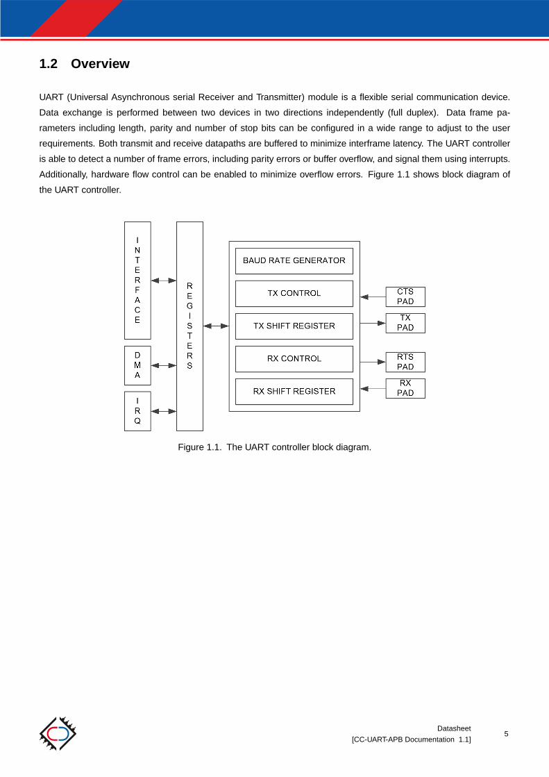
1.2 Overview
UART (Universal Asynchronous serial Receiver and Transmitter) module is a flexible serial communication device.
Data exchange is performed between two devices in two directions independently (full duplex). Data frame pa-
rameters including length, parity and number of stop bits can be configured in a wide range to adjust to the user
requirements. Both transmit and receive datapaths are buffered to minimize interframe latency. The UART controller
is able to detect a number of frame errors, including parity errors or buffer overflow, and signal them using interrupts.
Additionally, hardware flow control can be enabled to minimize overflow errors. Figure 1.1 shows block diagram of
the UART controller.
Figure 1.1. The UART controller block diagram.
Datasheet
[CC-UART-APB Documentation 1.1]5

1.3 Data Frame
Data exchange between two UART devices is performed using data frames. Each frame consists of synchronization
bits (start and stop), data bits and optional parity bit for error detection. The UART controller accepts the following
data frame configurations:
• 1 start bit,
• 5, 6, 7, 8 or 9 data bits (starting from MSB or LSB),
• 0 or 1 parity bit (even, odd, forced 1, forced 0),
• 1 or 2 stop bits.
Data frame starts with start bit (low level), after which data bits are sent. Then the optional parity bit is send followed
by one or two stop bits. Figure 1.2 presents the UART frame structure.
Figure 1.2. UART data frame format.
The UART controller is able to send and receive break frames (Figure 1.3). The break frame is a special case of
UART frame in which all bits, including stop bits, are zeros. The minimum length of the transmit and recognized break
frame depends on the UART frame configuration (number of data bits, stop bits etc.). The maximum length of the
UART break frame is not limited.
Figure 1.3. UART break frame.
After transmission of a break frame, the UART controller automatically sends one complete idle frame (all bits are
ones). This is done to ensure that the break frame end is detected properly by the external receiver. The UART
controller detects end of the break frame when two consecutive input samples are ones.
6Datasheet
[CC-UART-APB Documentation 1.1]

1.4 Data Sampling
The input RX signal can be sampled with 8 or 16 samples per data bit. However, only three middle samples are taken
into account while determining RX level. The sample pulse generator is highly configurable to allow wide range of
frequency ratios between desired baud rate and the UART module clock frequency. The UART transmitter utilizes
the same pulse generator as data receiver. The final configured baud rate depends on module frequency, OVRS8 bit
in CTRL register (1.9.4) and prescaler configuration in PRES register (1.9.3). It can be determined by the following
formulas:
OVRS8 Configured Baud Rate
0 BaudRate[pbs] =FPCLK [Hz]
16 ∗ (DIV _MAN +DIV _FRAC
16)
1 BaudRate[pbs] =FPCLK [Hz]
16 ∗ (DIV _MAN +DIV _FRAC
8)
Datasheet
[CC-UART-APB Documentation 1.1]7

1.5 Transmitter Module
Figure 1.4 presents the UART transmitter state diagram.
Figure 1.4. UART transmitter state diagram.
8Datasheet
[CC-UART-APB Documentation 1.1]
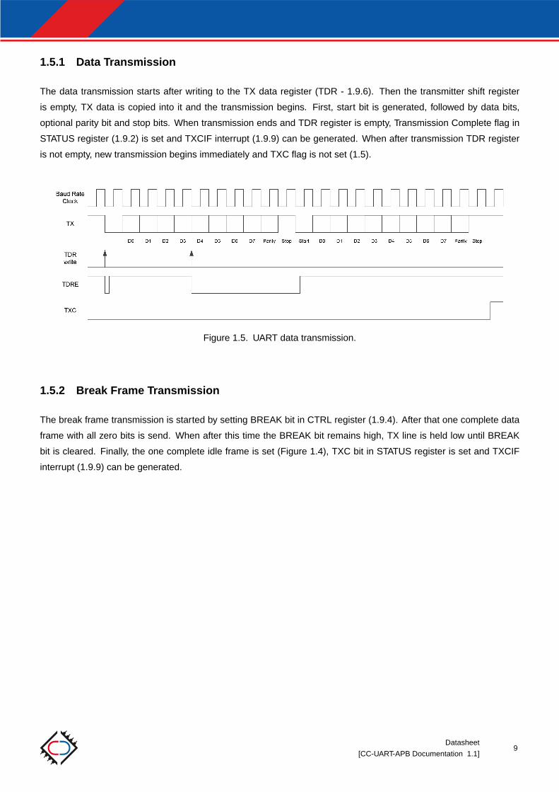
1.5.1 Data Transmission
The data transmission starts after writing to the TX data register (TDR - 1.9.6). Then the transmitter shift register
is empty, TX data is copied into it and the transmission begins. First, start bit is generated, followed by data bits,
optional parity bit and stop bits. When transmission ends and TDR register is empty, Transmission Complete flag in
STATUS register (1.9.2) is set and TXCIF interrupt (1.9.9) can be generated. When after transmission TDR register
is not empty, new transmission begins immediately and TXC flag is not set (1.5).
Figure 1.5. UART data transmission.
1.5.2 Break Frame Transmission
The break frame transmission is started by setting BREAK bit in CTRL register (1.9.4). After that one complete data
frame with all zero bits is send. When after this time the BREAK bit remains high, TX line is held low until BREAK
bit is cleared. Finally, the one complete idle frame is set (Figure 1.4), TXC bit in STATUS register is set and TXCIF
interrupt (1.9.9) can be generated.
Datasheet
[CC-UART-APB Documentation 1.1]9

1.5.3 RS485 Mode
In RS485 mode (Figure 1.6), UART module will automatically control RS485 driver output enable signal. Before the
transmission can start, module will set RTS line high for the pre-start period configured in the TMNG register (1.9.11).
RTS line will be held high for the transmission time and then for the configured post-stop time (1.9.11). When new
transmit data arrives before post-stop time ends, the transmission will start immediately without pre-start delay.
Figure 1.6. Connection of the RS485 transceiver.
RS485 mode can be enabled by setting RTSEN bit in CTRL register (1.9.4) and RS485EN bit in MODE register
(1.9.5). Figure 1.7 shows the exemplary waveform of RTS pin in RS485 mode.
Figure 1.7. RTS line in UART RS485 mode.
10Datasheet
[CC-UART-APB Documentation 1.1]
1.6 Data Reception
1.6.1 Frame Reception
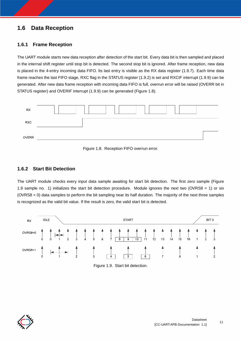
The UART module starts new data reception after detection of the start bit. Every data bit is then sampled and placed
in the internal shift register until stop bit is detected. The second stop bit is ignored. After frame reception, new data
is placed in the 4-entry incoming data FIFO. Its last entry is visible as the RX data register (1.9.7). Each time data
frame reaches the last FIFO stage, RXC flag in the STATUS register (1.9.2) is set and RXCIF interrupt (1.9.9) can be
generated. After new data frame reception with incoming data FIFO is full, overrun error will be raised (OVERR bit in
STATUS register) and OVERIF interrupt (1.9.9) can be generated (Figure 1.8).
Figure 1.8. Reception FIFO overrun error.
1.6.2 Start Bit Detection
The UART module checks every input data sample awaiting for start bit detection. The first zero sample (Figure
1.9 sample no. 1) initializes the start bit detection procedure. Module ignores the next two (OVRS8 = 1) or six
(OVRS8 = 0) data samples to perform the bit sampling near its half duration. The majority of the next three samples
is recognized as the valid bit value. If the result is zero, the valid start bit is detected.
Figure 1.9. Start bit detection.
Datasheet
[CC-UART-APB Documentation 1.1]11

1.6.3 Data Bits Detection
Data and parity bits are sampled 8 or 16 samples per bit (Figure 1.10). Similarly like in start bit detection, the majority
of three middle samples is used to determine bit value. The data bits are sampled to the first stop bit, whereas the
possible second one is ignored.
Figure 1.10. Data bits detection.
1.6.4 Stop Bit Detection
Figure 1.11 shows the stop bit sampling. Similarly like in other frame bits, the majority of three middle samples is
used to determine bit value. The only difference is that, after getting stop bit middle three samples, module is not
waiting to the end of bit transmission, but immediately ends frame reception. When detected bit value is zero, frame
is considered invalid, FRERR bit is set in status register (1.9.2) and FERIF interrupt (1.9.9) can be generated.
Figure 1.11. Stop bit detection.
12Datasheet
[CC-UART-APB Documentation 1.1]

1.6.5 Receiver Error Flags
UART receiver module uses STATUS register to store error flags of the following events:
• PERR – Parity error. Bit is set if parity bit of received frame does not match the expected one. Bit is updated
together with the RXC bit in the STATUS register.
• FRERR – Frame error. Bit is set when expected stop bit value is zero. Bit is updated together with the RXC bit in
the STATUS register.
• OVERR – Overrun error. Bit is set if UART receives new data frame when incoming data FIFO is full. Bit is
updated together with the RXC bit in the STATUS register.
• RXBRK – Break frame reception. RXC bit will be set when break frame receiving ends.
Datasheet
[CC-UART-APB Documentation 1.1]13

1.7 Hardware Flow Control
UART hardware flow control uses a pair of signals - RTS and CTS. They are used to signal to the remote transmitter if
module can accept data and detect if a remote receiver is ready to accept new data. The implemented UART module
allows to independently set RTS (RTSEN - 1.9.4) and CTS (CTSEN - 1.9.4) flow control.
1.7.1 RTS Line
The RTS line (Request To Send) is used to signal to the remote transmitter if module can accept data. The UART
receiver module consists of 4-entry incoming data FIFO. The RTS line will be deasserted (high) as soon as three
FIFO entries are occupied (1.12). This will allow the remote transceiver to finish transmission of the forth frame if
already began and prevent receiver overrun. The UART module will assert (low) RTS line if there is two or more free
entries in the FIFO. RTS flow control can be enabled by setting RTSEN bit in CTRL register (1.9.4).
Figure 1.12. RTS hardware flow control.
14Datasheet
[CC-UART-APB Documentation 1.1]

1.7.2 CTS Line
The CTS line (Clear To Send) is used to detect if a remote receiver is ready to accept new data. The UART module
will not start any transmission as long as it detects the CTS line deasserted (high). CTS flow control can be enabled
by setting CTSEN bit in CTRL register (1.9.4).
1.7.3 Pad Output Enable
The UART module has two output ports - TX and RTS. The TX pad output enable signal is enabled as soon as TXEN
bit in CTRL register (1.9.4) is set. The behaviour of RTS pad and RTS pad output enable signal depends on the
module operation mode. In RS485 mode RTS line is used to control RS485 driver output enable signal, otherwise it
is used to perform hardware flow control. Figure 1.13 presents the behaviour of RTS output enable signal in different
operating modes.
Figure 1.13. RTS pad output enable signal.
Datasheet
[CC-UART-APB Documentation 1.1]15

1.8 Interrupts
The UART controller may rise interrupts according to one or more configurable events.
The interrupt source can be determined in interrupt flags register (IRQF - 1.9.9). The interrupt line is kept asserted
as long as the interrupt flag bit is high. Interrupt flags can be cleared by writing one to appropriate bit in interrupt flags
register. The interrupt source can be enabled or disabled by configuring interrupt mask register (IRQM - 1.9.8).
1.8.1 TXC Interrupt
Interrupt is raised when the frame transmitting ends and TDR register (1.9.6) is empty.
1.8.2 RXC Interrupt
Interrupt is raised when new frame receiving ends.
1.8.3 TXDRE Interrupt
Interrupt is raised when TDR register (1.9.6) is empty. At the same time the previous data transmission can be in
progress.
1.8.4 Parity Error Interrupt
Interrupt is raised when received frame has a parity error.
1.8.5 Framing Error Interrupt
Interrupt is raised when invalid stop bit is received.
16Datasheet
[CC-UART-APB Documentation 1.1]

1.8.6 Overrun Error Interrupt
Interrupt is raised when incoming data FIFO is overrun and loss of data occured.
1.8.7 Break Reception Started Interrupt
Interrupt is raised when the minimal length break frame is received. The break frame receiving can still be in progress.
1.8.8 Break Reception Ended Interrupt
Interrupt is raised when controller detects end of break frame receiving.
1.8.9 CTS Rising Interrupt
Interrupt is raised if CTS pad raising edge was detected.
Datasheet
[CC-UART-APB Documentation 1.1]17

1.9 Configuration Registers
1.9.1 Registers List
Address Offset Register Name
0x00 STATUS Status Register
0x04 PRES Prescaler Register
0x08 CTRL Control Register
0x0C MODE Mode Register
0x10 TDR Transmit Data Register
0x14 RDR Receive Data Register
0x18 IRQM Interrupt Mask Register
0x1C IRQF Interrupt Flags Register
0x20 IRQMAP Interrupt Mapping Register
0x24 TMNG RS485 Timings Register
1.9.2 Status Register
Address: 0x00
31
R
0
30
R
0
. . .
. . .
R
0
. . .
. . .
R
0
. . .
. . .
R
0
. . .
. . .
R
0
9
R
0
8
R
0
7
CTS
R
0
6
RXBRK
R
0
5
OVERR
R
0
4
FRERR
R
0
3
PERR
R
0
2
TXDRE
R
1
1
TXC
R
0
0
RXC
R
0
RXC Reception Complete
0 No valid data in RDR register.
1 New valid data in RDR register. Other frame status bits are valid.
Bit is set when new frame arrives and is cleared after reading RDR register.
TXC Transmission Complete
0 Transmission is in progress.
1 There is no transmission in progress and no valid data is in TDR register.
Bit is set after finishing transmission of the last data frame. Bit is cleared after writing to TDR register.
18Datasheet
[CC-UART-APB Documentation 1.1]

TXDRE Transmission Data Register Empty
0 TDR contains data to be transmitted.
1 TDR register is empty.
Bit is set after transferring TDR data into the internal transmitter shift register. Bit is cleared after writing to the
TDR register.
PERR Parity Error
0 Parity bit is correct.
1 Parity bit is incorrect.
Bit is valid only when RXC bit is set.
FRERR Framing Error
0 Received frame is correct.
1 Received frame is incorrect.
Bit is valid only when RXC bit is set. Bit signals that received stop bit is incorrect.
OVERR Overrun Error
0 No overrun error detected.
1 Overrun error detected.
Bit is valid when RXC bit is set.
RXBRK Break Reception
0 No break frame received.
1 Break frame received.
Bit is set when break frame was received. As break frame has undefined length, its end is determined by RXBRK
and RXC bits. RXBRK bit is cleared after reading RDR register or after receiving new data frame.
RXBRK RXC Status
1 0 Break frame receiving is in progress.
1 1 Break frame receiving ended.
0 - No break frame received.
CTS CTS Status
When CTS flow control is enabled, bit reflects the CTS line state.
Datasheet
[CC-UART-APB Documentation 1.1]19

1.9.3 Prescaler Register
Address: 0x04
31
R
0
30
R
0
. . .
. . .
R
0
. . .
. . .
R
0
. . .
. . .
R
0
26
R
0
25
R
0
24
R
0
23
R
0
22
R
0
21
R
0
20
R
0
19 16
DFRAC[3:0]
R/W
0
15 8
DMNT[15:8]
R/W
0
7 0
DMNT[7:0]
R/W
0
DMNT[15:0] Prescaler Mantissa
Integer part of baud rate generator prescaler.
0 Generator is disabled.
1-65535 Valid prescaler data, generator is enabled.
DFRAC[3:0] Division Fraction
Fractional part of baud rate generator prescaler. When OVRS8 bit is high, the fractional part equalsDIV _FRAC[18 : 16]
8. Otherwise the fractional part equals
DIV _FRAC[19 : 16]
16.
Baud rate generator configuration should be changed only when both receiver and transmitter are disabled (TXEN =
0 and RXEN = 0).
20Datasheet
[CC-UART-APB Documentation 1.1]

1.9.4 Control Register
Address: 0x08
31
R
0
30
R
0
. . .
. . .
R
0
. . .
. . .
R
0
. . .
. . .
R
0
. . .
. . .
R
0
9
R
0
8
R
0
7
R
0
6
R
0
5
LOOP
R/W
0
4
BREAK
R/W
0
3
CTSEN
R/W
0
2
RTSEN
R/W
0
1
RXEN
R/W
0
0
TXEN
R/W
0
TXEN Transmitter Enable
0 Transmitter module is disabled.
1 Transmitter module is enabled.
RXEN Receiver Enable
0 Receiver module is disabled.
1 Receiver module is enabled.
RTSEN RTS Hardware Support Enable
0 RTS hardware support is disabled.
1 RTS hardware support is enabled.
If RS485EN bit is disabled, RTS takes part in hardware flow control. Otherwise RTS line is used to control RS485
driver output enable signal.
CTSEN CTS Hardware Support Enable
0 CTS hardware flow control is disabled.
1 CTS hardware flow control is enabled.
BREAK Break Frame Transmit
After setting this bit, module starts to transmit break frame. The break frame will be transmitted as long as this
bit is set but no shorter than for one valid data frame time. An idle frame is transmitted directly after transmitting
break frame.
Datasheet
[CC-UART-APB Documentation 1.1]21
LOOP Loopback Mode Enable
0 Loopback mode is disabled.
1 Loopback mode is enabled.
In loopback mode the transmitted output is connected to the TX pad and directly to the receiver input.
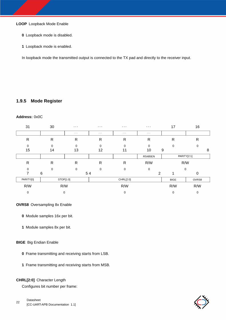
1.9.5 Mode Register
Address: 0x0C
31
R
0
30
R
0
. . .
. . .
R
0
. . .
. . .
R
0
. . .
. . .
R
0
. . .
. . .
R
0
17
R
0
16
R
0
15
R
0
14
R
0
13
R
0
12
R
0
11
R
0
10
RS485EN
R/W
0
9 8
PARITY[2:1]
R/W
0
7
PARITY[0]
R/W
0
6 5
STOP[1:0]
R/W
0
4 2
CHRL[2:0]
R/W
0
1
BIGE
R/W
0
0
OVRS8
R/W
0
OVRS8 Oversampling 8x Enable
0 Module samples 16x per bit.
1 Module samples 8x per bit.
BIGE Big Endian Enable
0 Frame transmitting and receiving starts from LSB.
1 Frame transmitting and receiving starts from MSB.
CHRL[2:0] Character Length
Configures bit number per frame:
22Datasheet
[CC-UART-APB Documentation 1.1]

CHRL[2:0] Data bits number
000 8
001 7
010 6
011 5
100 9
101-111 RFU
STOP[1:0] Stop Bits Number
Configures number of stop bits per frame:
STOP[1:0] Stop bits number
00 1
01 2
1- RFU
PAR[2:0] Parity Configuration
Parity configuration:
PAR[2:0] Parity configuration
000 No
001 Even
010 Odd
011 Forced 0
100 Forced 1
101-111 RFU
RS485EN RS485 Mode Enable
RTS line configuration:
RTSEN RXEN TXEN RS485EN Mode
1 1 - 0 RTS hardware flow control.
1 - 1 1 RTS RS485 mode.
0 - - - RTS output is disabled.
Datasheet
[CC-UART-APB Documentation 1.1]23
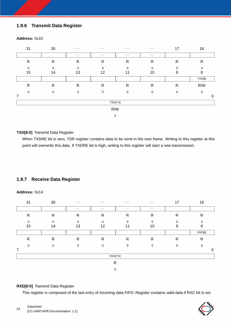
1.9.6 Transmit Data Register
Address: 0x10
31
R
0
30
R
0
. . .
. . .
R
0
. . .
. . .
R
0
. . .
. . .
R
0
. . .
. . .
R
0
17
R
0
16
R
0
15
R
0
14
R
0
13
R
0
12
R
0
11
R
0
10
R
0
9
R
0
8
TXD[8]
R/W
0
7 0
TXD[7:0]
R/W
0
TXD[8:0] Transmit Data Register
When TXDRE bit is zero, TDR register contains data to be send in the next frame. Writing to this register at this
point will overwrite this data. If TXDRE bit is high, writing to this register will start a new transmission.
1.9.7 Receive Data Register
Address: 0x14
31
R
0
30
R
0
. . .
. . .
R
0
. . .
. . .
R
0
. . .
. . .
R
0
. . .
. . .
R
0
17
R
0
16
R
0
15
R
0
14
R
0
13
R
0
12
R
0
11
R
0
10
R
0
9
R
0
8
RXD[8]
R
0
7 0
RXD[7:0]
R
0
RXD[8:0] Transmit Data Register
This register is composed of the last entry of incoming data FIFO. Register contains valid data if RXC bit is set.
24Datasheet
[CC-UART-APB Documentation 1.1]
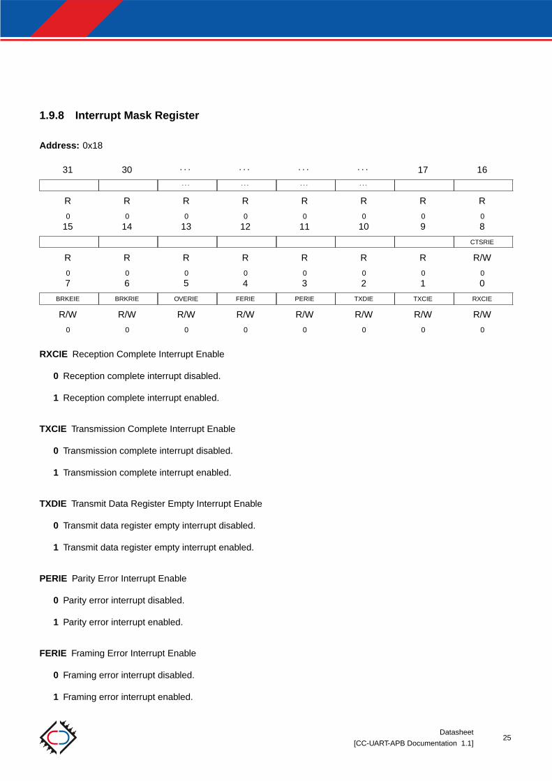
1.9.8 Interrupt Mask Register
Address: 0x18
31
R
0
30
R
0
. . .
. . .
R
0
. . .
. . .
R
0
. . .
. . .
R
0
. . .
. . .
R
0
17
R
0
16
R
0
15
R
0
14
R
0
13
R
0
12
R
0
11
R
0
10
R
0
9
R
0
8
CTSRIE
R/W
0
7
BRKEIE
R/W
0
6
BRKRIE
R/W
0
5
OVERIE
R/W
0
4
FERIE
R/W
0
3
PERIE
R/W
0
2
TXDIE
R/W
0
1
TXCIE
R/W
0
0
RXCIE
R/W
0
RXCIE Reception Complete Interrupt Enable
0 Reception complete interrupt disabled.
1 Reception complete interrupt enabled.
TXCIE Transmission Complete Interrupt Enable
0 Transmission complete interrupt disabled.
1 Transmission complete interrupt enabled.
TXDIE Transmit Data Register Empty Interrupt Enable
0 Transmit data register empty interrupt disabled.
1 Transmit data register empty interrupt enabled.
PERIE Parity Error Interrupt Enable
0 Parity error interrupt disabled.
1 Parity error interrupt enabled.
FERIE Framing Error Interrupt Enable
0 Framing error interrupt disabled.
1 Framing error interrupt enabled.
Datasheet
[CC-UART-APB Documentation 1.1]25

OVERIE Overrun Error Interrupt Enable
0 Overrun error interrupt disabled.
1 Overrun error interrupt enabled.
BRKRIE Break Reception Start Interrupt Enable
0 Break reception start interrupt disabled.
1 Break reception start interrupt enabled.
BRKEIE Break Reception End Interrupt Enable
0 Break reception end interrupt disabled.
1 Break reception end interrupt enabled.
CTSRIE Rising Edge on CTS Line Interrupt Enable
0 Rising edge on CTS line interrupt disabled.
1 Rising edge on CTS line interrupt enabled.
1.9.9 Interrupt Flags Register
Address: 0x1C
31
R
0
30
R
0
. . .
. . .
R
0
. . .
. . .
R
0
. . .
. . .
R
0
. . .
. . .
R
0
17
R
0
16
R
0
15
R
0
14
R
0
13
R
0
12
R
0
11
R
0
10
R
0
9
R
0
8
CTSREIF
R/W
0
7
BRKEIF
R/W
0
6
BRKRIF
R/W
0
5
OVERIF
R/W
0
4
FERIF
R/W
0
3
PERIF
R/W
0
2
TXDIF
R/W
0
1
TXCIF
R/W
0
0
RXCIF
R/W
0
RXCIF Reception Complete Interrupt Flag
Data frame reception completed.
TXCIF Transmission Complete Interrupt Flag
Transmission completed. TDR register is empty.
26Datasheet
[CC-UART-APB Documentation 1.1]

TXDIF Transmit Data Register Empty Interrupt Flag
TDR register is empty.
PERIF Parity Error Interrupt Flag
Parity error occured.
FERIF Framing Error Interrupt Flag
Framing error occured.
OVERIF Overrun Error Interrupt Flag
Overrun error occured.
BRKRIF Break Reception Start Interrupt Flag
Receiver module detected start of the break frame.
BRKEIF Break Reception End Interrupt Flag
Break frame reception ended.
CTSREIF Rising Edge on CTS Line Interrupt Flag
Rising edge on CTS line occured.
Every bit in the register can be cleared after writing one to the corresponding position.
1.9.10 Interrupt Mapping Register
Address: 0x20
31
R
0
30
R
0
. . .
. . .
R
0
. . .
. . .
R
0
. . .
. . .
R
0
. . .
. . .
R
0
17
R
0
16
R
0
15 8
IRQMAP[15:8]
R/W
IRQMAP[15:8]
7 1
IRQMAP[7:1]
R/W
IRQMAP[7:1]
0
R
0
Datasheet
[CC-UART-APB Documentation 1.1]27
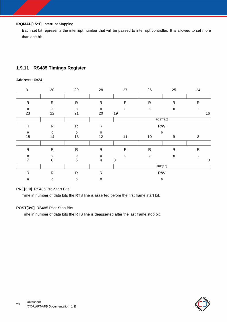
IRQMAP[15:1] Interrupt Mapping
Each set bit represents the interrupt number that will be passed to interrupt controller. It is allowed to set more
than one bit.
1.9.11 RS485 Timings Register
Address: 0x24
31
R
0
30
R
0
29
R
0
28
R
0
27
R
0
26
R
0
25
R
0
24
R
0
23
R
0
22
R
0
21
R
0
20
R
0
19 16
POST[3:0]
R/W
0
15
R
0
14
R
0
13
R
0
12
R
0
11
R
0
10
R
0
9
R
0
8
R
0
7
R
0
6
R
0
5
R
0
4
R
0
3 0
PRE[3:0]
R/W
0
PRE[3:0] RS485 Pre-Start Bits
Time in number of data bits the RTS line is asserted before the first frame start bit.
POST[3:0] RS485 Post-Stop Bits
Time in number of data bits the RTS line is deasserted after the last frame stop bit.
28Datasheet
[CC-UART-APB Documentation 1.1]

1.10 Implementation
1.10.1 Design Structure
The synthesible RTL IP core part (COMMON/rtl and UART/rtl folder) utilizes Verilog 2005 HDL. The testbench part
(UART/tb folder) uses SystemVerilog language.
COMMONrtl
DFF_en.vedge_detector.vsynchronizer.v
UARTbehrtl
APB_UART.vbaud_rate_generator.vRX_fifo.vRX_module.vRX_module.vUART_config.vUART_defines.vUART_PDMA_stream_interface.vUART.v
tbcommon
timescale.vrun
ncvlog_apb_uart.shtasks
APBtb_APB_UART_init.vtb_APB_UART_reg_access_tasks.v
commontb_UART_config_tasks.vtb_UART_data_transfer_tasks.vvirtual_UART.v
UARTtb_UART_init.vtb_UART_reg_access_tasks.v
teststb_break_test.vtb_CTS_test.vtb_FrameErr_test.vtb_interrupt_MAPPING_test.vtb_interrupt_test.vtb_OverErr_test.vtb_ParityErr_test.vtb_PDMA_interface_TX_and_RX_test.svtb_RS485_RTS_break_test.vtb_RS485_RTS_test.vtb_RTS_test.vtb_RX_test.vtb_TX_and_RX_test.vtb_TX_test.v
Datasheet
[CC-UART-APB Documentation 1.1]29

tb_APB_UART.svtb_baud_rate_generator.vtb_UART.vtb_virtual_UART.v
compile.list
1.10.2 Simulation Flow
The IP Core is provided with self-checking testbench to verify the correct operation of the IP prior to use in a
design. To run the simulation using Cadence R© Incisive R© Enterprise Simulator run ncvlog_apb_uart.sh script located
in UART/tb/run folder. The simulation should end with reporting no errors.
1.10.3 Clock and Reset
The CC-UART-APB utilizes a fully synchronous design with one positive edge clocking domain and negative asyn-
chronous reset assertion. External reset synchronizer has to be used to ensure synchronous reset deassertion.
1.10.4 Constraints
In most cases only module output ports are registered. Therefore, it is a good practice to reserve the entire clock
cycle for module inputs combinational logic and set minimal input delay (set_input_delay command). Registered
outputs leave the entire clock cycle for external logic (set_output_delay command).
External module inputs are synchronized using Synchronizer module located in the synchronizer.v file. If possible,
they should be replaced with integrated 2FF synchronizers from the target technology library. Otherwise, max delay
(set_max_delay command) of 10% to 20% of one destination clock cycle should be set between synchronizer stages.
Do not use dynamic FFs to implement synchronizer module.
30Datasheet
[CC-UART-APB Documentation 1.1]

1.10.5 Configuration Options
The table below shows the generic parameters of the core.
Generic name Description Range Default
PDMA_support Configure PDMA interface support 0,1 1
default_interrupt_MAPPING Reset value of interrupt_MAPPING register 0:32767 0
Datasheet
[CC-UART-APB Documentation 1.1]31

1.10.6 Signals Description
Signal name Description I/O Active Type
PCLK Synchronous clock I rising clock
PRESETn Asynchronous reset I low reset
PSEL APB peripheral select I high comb.
PENABLE APB bus enable I high comb.
PADDR[5:2] APB bus address I data comb.
PWRITE APB bus write I high comb.
PWDATA[31:0] APB bus write data I data comb.
PREADY APB bus ready O high const.
PRDATA[31:0] APB bus read data O data reg.
interrupt_RX_finished Reception complete interrupt O high reg.
interrupt_TX_finished Transmission finished interrupt O high reg.
interrupt_TX_data_reg_empty TX data register empty interrupt O high reg.
interrupt_PARITY_error Parity error interrupt O high reg.
interrupt_FRAMING_error Framing error interrupt O high reg.
interrupt_OVERRUN_error Overrun error interrupt O high reg.
interrupt_BREAK_receiving Break frame detected interrupt O high reg.
interrupt_BREAK_ended End of break detected interrupt O high reg.
interrupt_CTS_falling_edge CTS falling edge interrupt O high reg.
interrupt_MAPPING[15:1] Interrupt mapping vector O data reg.
Downstream_enable PDMA downstream enable signal I high comb.
Downstream_busy PDMA downstream busy signal O high reg.
Downstream_request PDMA downstream request signal O high reg.
Downstream_ack PDMA downstream ack signal I high comb.
Downstream_data[31:0] PDMA downstream data I data comb.
Upstream_enable PDMA upstream enable signal I high comb.
Upstream_busy PDMA upstream busy signal O high reg.
Upstream_request PDMA upstream request signal O high reg.
Upstream_ack PDMA upstream ack signal I high comb.
Upstream_data[31:0] PDMA upstream data O data reg.
clock_request Clock request signal O high reg.
CTS_pad UART CTS pad I low reg.
RX_pad UART RX pad I data reg.
TX_pad UART TX pad O data reg.
TX_pad_oe UART TX pad output enable O high reg.
RTS_pad UART RTS pad O low or high1 reg.
RTS_pad_oe UART RTS pad output enable O high reg.
1 Signal is active low in RTS hardware flow control mode and high in RS485 mode.
32Datasheet
[CC-UART-APB Documentation 1.1]

1.10.7 Instantiation
icg
icg_uart (
.E(uart_PSEL|uart_clock_request),
.clk(PCLK),
.gclk(uart_clk),
.scan_enable(scan_enable));
APB_UART #(
.PDMA_support(CFG_DMA_EN),
.default_interrupt_MAPPING(CFG_DEF_INT_MAPPING))
APB_UART_u (
.PCLK(uart_clk),
.PRESETn(rst),
.PSEL(uart_PSEL),
.PENABLE(uart_PENABLE),
.PADDR(PADDR[5:2]),
.PWRITE(PWRITE),
.PWDATA(PWDATA),
.PREADY(uart_PREADY),
.PRDATA(uart_PRDATA),
.CTS_pad(CTS),
.RX_pad(RX),
.TX_pad(TX),
.TX_pad_oe(TX_oe),
.RTS_pad(RTS),
.RTS_pad_oe(RTS_oe),
.interrupt_RX_finished(uart_interrupt_RX_finished),
.interrupt_TX_finished(uart_interrupt_TX_finished),
.interrupt_TX_data_reg_empty(uart_interrupt_TX_data_reg_empty),
.interrupt_PARITY_error(uart_interrupt_PARITY_error),
.interrupt_FRAMING_error(uart_interrupt_FRAMING_error),
.interrupt_OVERRUN_error(uart_interrupt_OVERRUN_error),
.interrupt_BREAK_receiving(uart_interrupt_BREAK_receiving),
.interrupt_BREAK_ended(uart_interrupt_BREAK_ended),
.interrupt_CTS_falling_edge(uart_interrupt_CTS_falling_edge),
.interrupt_MAPPING(uart_interrupt_MAPPING),
.Downstream_enable(uart_downstream_enable),
.Downstream_busy(uart_downstream_busy),
.Downstream_request(uart_downstream_request),
Datasheet
[CC-UART-APB Documentation 1.1]33

.Downstream_ack(uart_downstream_ack),
.Downstream_data(downstream_data),
.Upstream_enable(uart_upstream_enable),
.Upstream_busy(uart_upstream_busy),
.Upstream_request(uart_upstream_request),
.Upstream_ack(uart_upstream_ack),
.Upstream_data(uart_upstream_data),
.clock_request(uart_clock_request));
assign uart_irq = uart_interrupt_RX_finished |
uart_interrupt_TX_finished |
uart_interrupt_TX_data_reg_empty |
uart_interrupt_PARITY_error |
uart_interrupt_FRAMING_error |
uart_interrupt_OVERRUN_error |
uart_interrupt_BREAK_receiving |
uart_interrupt_BREAK_ended |
uart_interrupt_CTS_falling_edge;
assign uart_irq_vector = uart_interrupt_MAPPING & {15{uart_irq}};
io_pad_model #(
.IO_NUM(1))
tx_pad_model (
.core_input(1’b0),
.core_output(TX),
.IO_pad(TX_pad),
.output_enable(TX_oe));
io_pad_model #(
.IO_NUM(1))
rts_pad_model (
.core_input(1’b0),
.core_output(RTS),
.IO_pad(RTS_pad),
.output_enable(RTS_oe));
io_pad_model #(
.IO_NUM(1))
rx_pad_model (
.core_input(RX),
.core_output(1’b0),
34Datasheet
[CC-UART-APB Documentation 1.1]
.IO_pad(RX_pad),
.output_enable(1’b0));
io_pad_model #(
.IO_NUM(1))
cts_pad_model (
.core_input(CTS),
.core_output(1’b0),
.IO_pad(CTS_pad),
.output_enable(1’b0));
Datasheet
[CC-UART-APB Documentation 1.1]35

1.11 Revision History
Doc. Rev. Date Comments
1.1 11-2018 Editorial corrections in 1.10.7 Instantiation section.
1.0 12-2017 First Issue.
36Datasheet
[CC-UART-APB Documentation 1.1]
ChipCraft Sp. z o.o. Dobrzanskiego 3 lok. BS073, 20-262 Lublin, POLAND www.chipcraft-ic.com
c©2018 ChipCraft Sp. z o.o. CC-UART-APB-Doc_112018.
ChipCraft R©, ChipCraft logo and combination of thereof are registered trademarks or trademarks of ChipCraft Sp. z o.o. All other names are theproperty of their respective owners.
Disclaimer: ChipCraft makes no representations or warranties with respect to the accuracy or completeness of the contents of this documentand reserves the right to make changes to specifications and product descriptions at any time without notice. ChipCraft does not make anycommitment to update the information contained herein.


![[PPT]UART and UART Driver - University at Buffalobina/cse321/fall2009/UARTDriver.ppt · Web viewUART and UART Driver B. Ramamurthy * UART UART: Universal Asynchronous Receiver/Transmitter](https://static.fdocuments.us/doc/165x107/5b2ab3637f8b9a55068b752f/pptuart-and-uart-driver-university-at-binacse321fall2009uartdriverppt.jpg)
