
DATA SHEET - Panasonic of Power LSI . 27 AN41908A SDB00179AEB 3 AN41908A Lens Driver IC for...
27
1 Publication date: February 2010 SDB00179AEB DATA SHEET Part No. Package Code No. AN41908A ∗QFN044-P-0606D
Transcript of DATA SHEET - Panasonic of Power LSI . 27 AN41908A SDB00179AEB 3 AN41908A Lens Driver IC for...

1Publication date: February 2010 SDB00179AEB
DATA SHEET
Part No.
Package Code No.
AN41908A∗QFN044-P-0606D
AN41908A
2SDB00179AEB
ContentsOverview …………………………………………………………………………………………………………… 3
Features …………………………………………………………………………………………………………… 3
Applications ………………………………………………….…………………………………………………….. 3
Package …………………………………………………………………………………………………………… 3
Type ……………………………………………………….…………………………………………………………. 3
Application Circuit Example ……………………………………………………………………………………… 4
Block Diagram ……………………………………………….……………………………………………………. 5
Pin Descriptions ………………………………………….………………………………………………………… 6
Absolute Maximum Ratings ……………………………….……………………………………………………… 8
Operating Supply Voltage Range …………………….…………………………………………………………… 8
Allowable Current and Voltage Range ………………………………………………………………………….. 9
Electrical Characteristics …………….…………………………………………………………………………… 10
Electrical Characteristics (Reference values for design) ……………………………………………………… 12
Technical Data ………………………………………….…………………………………………………………… 14
I/O block circuit diagrams and pin function descriptions …………………………………………………….. 14
PD ⎯ Ta diagram ………………………………………………………………………………………………… 25
Usage Notes ………………………………………….……………………………………………………………. 26
Special attention and precaution in using ………………………………………………………………………. 26
Notes of Power LSI ………………………………………………………………………………………………. 27

AN41908A
3SDB00179AEB
AN41908ALens Driver IC for camcorder and security-camera incorporating Iris control
OverviewAN41908A is a lens motor driver IC for camcorder and security-camera featuring the functions of Iris control. Voltage drive system
and several torque ripple correction techniques enable super- low noise microstep drive.
FeaturesVoltage drive system 256-step microstep drivers (2 systems)Built-in Iris controllerMotor control by 4-line serial data communication2 systems of open-drain for driving LED
ApplicationsCamcorder, Security-camera
Package44 pin Plastic Quad Flat Non-leaded Package (QFN Type)
TypeBi-COMS IC

AN41908A
4SDB00179AEB
Application Circuit Example
Note) This application circuit is shown as an example but does not guarantee the design for mass production set.
V+
V–
1
2
3
4
5
6
7
8
9
10
11
OP3INP
SENS
OP3OUT
REF
AVDD3
ADTESTIN
TEST
OUTE2
VDD5
GND5
OUTE1
12 13 14 15 16 17 18 19 20 21 22
N.C
.
OU
TD2
OU
TD1
MG
ND
B
OU
TC2
OU
TC1
MV
CC
B
OU
TB2
OU
TB1
OU
TA2
MV
CC
A
44 43 42 41 40 39 38 37 36 35 34
PLS1
SIN
VD
_FZ
VD
_IS
RST
B
OP4
OU
T
OP4
INN
VR
EF
GN
DA
CR
EFIN
PLS2
23
33
32
31
30
29
28
27
26
25
24 MGNDA
OUTA1
N.C.
SCK
SOUT
CS
GNDD
LED2
LED1
OSCIN
DVDD
HallSensorH– H+
8.2 kΩ0.
1 μF
100
pF
0.1
μF
10 kΩAVDD3(3.1 V)
MVDD5(4.8 V)
MVCCB(4.8 V)
MVCCA(4.8 V)
DVDD(3.1 V)
0.01 μF

AN41908A
5SDB00179AEB
Block Diagram
Note) This block diagram is for explaining functions. The part of the block diagram may be omitted, or it may be simplified.
1
2
3
4
5
6
7
8
9
10
11
OP3INP
SENS
OP3OUT
REF
AVDD3
ADTESTIN
TEST
OUTE2
VDD5
GND5
OUTE1
12 13 14 15 16 17 18 19 20 21 22
N.C
.
OU
TD2
OU
TD1
MG
ND
B
OU
TC2
OU
TC1
MV
CC
B
OU
TB2
OU
TB1
OU
TA2
MV
CC
A
44 43 42 41 40 39 38 37 36 35 34
PLS1
SIN
VD
_FZ
VD
_IS
RST
B
OP4
OU
T
OP4
INN
VR
EF
GN
DA
CR
EFIN
PLS2
23
33
32
31
30
29
28
27
26
25
24 MGNDA
OUTA1
N.C.
SCK
SOUT
CS
GNDD
LED2
LED1
OSCIN
DVDD8 bitDAC
AVDD3(3.1 V)
8-bitCurrent
Adj
LEDDr.
Pulse generator
SIF
controllogic
10 bitADC
IRISDriver
PWM DutyControl
Driver ADriver BDriver CDriver D
UVLO
Driver A to D
TSD

AN41908A
6SDB00179AEB
Pin Descriptions
Hall signal amplifier non-inverting inputInputOP3INP1
Hall current bias outputOutputSENS2
Hall signal amplifier outputOutputOP3OUT3
Resistor connection for Hall current bias setting—REF4
3 V analog power supplyPower supplyAVDD35
ADC test inputInputADTESTIN6
Test mode inputInputTEST7
Motor output E2OutputOUTE28
Power supply for IrisPower supplyVDD59
GND for IrisGroundGND510
Motor output E1OutputOUTE111
N.C.—N.C.12
Motor output D2OutputOUTD213
Power supply for motor BPower supplyMVCCB14
Motor output D1OutputOUTD115
Motor output C2OutputOUTC216
GND for motor BGroundMGNDB17
Motor output C1OutputOUTC118
Motor output B2OutputOUTB219
Power supply for motor APower supplyMVCCA20
Motor output B1OutputOUTB121
Motor output A2OutputOUTA222
N.C.—N.C.23
GND for motor AGroundMGNDA24
Motor output A1OutputOUTA125
Open-drain 1 for driving LEDInputLED126
Open-drain 2 for driving LED InputLED227
Digital GNDGroundGNDD28
OSCIN inputInputOSCIN29
3 V digital power supplyPower supplyDVDD30
Serial data outputOutputSOUT31
Chip select signal inputInputCS32
Serial clock inputInputSCK33
Serial data inputInputSIN34
Iris video sync. signal inputInputVD_IS35
DescriptionTypePin namePin No.
AN41908A
7SDB00179AEB
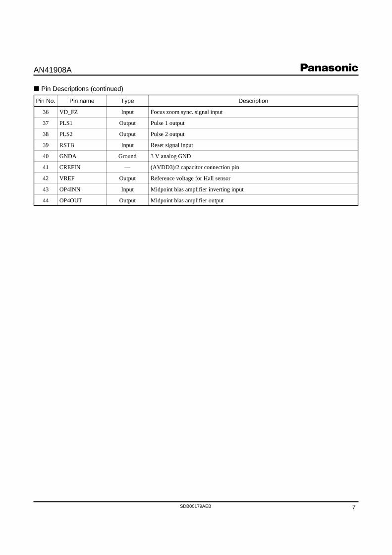
Pin Descriptions (continued)
Focus zoom sync. signal inputInputVD_FZ36
Pulse 1 outputOutputPLS137
Pulse 2 outputOutputPLS238
Reset signal inputInputRSTB39
3 V analog GNDGroundGNDA40
(AVDD3)/2 capacitor connection pin—CREFIN41
Reference voltage for Hall sensorOutputVREF42
Midpoint bias amplifier inverting inputInputOP4INN43
Midpoint bias amplifier outputOutputOP4OUT44
DescriptionTypePin namePin No.

AN41908A
8SDB00179AEB
Absolute Maximum Ratings
—A/ch±0.4IM(pulse)Instantaneous H bridge drive current9
*3°C–20 to + 85ToprOperating ambient temperature5
*2mW141.4PDPower dissipation4
*1V– 0.3 to + 6.0VDD5Supply voltage for motor controller 23
*1V– 0.3 to + 6.0MVCCxSupply voltage for motor controller 1 2
*3°C–55 to + 125TstgStorage temperature6
– 0.3 to + 4.0DVDD
NotesUnitRatingSymbolParameterA No.
*4V– 0.3 to (DVDD + 0.3)VinDigital input voltage10
—A/ch±0.15IM2(CD)Motor driver 2 (iris)H bridge drive current8
—A/ch±0.25IM1(CD)Motor driver 1 (focus, zoom)H bridge drive current7
*1V– 0.3 to + 4.0AVDD3
Controller supply voltage1
Notes) *1 : The values under the condition not exceeding the above absolute maximum ratings and the power dissipation.*2 : The power dissipation shown is the value at Ta = 85°C for the independent (unmounted) IC package without a heat sink.
When using this IC, refer to the • PD-Ta diagram in the Technical Data and design the heat radiation with sufficient margin so that theallowable value might not be exceeded based on the conditions of power supply voltage, load, and ambient temperature.
*3 : Except for the power dissipation, operating ambient temperature, and storage temperature, all ratings are for Ta = 25°C.*4 : (DVDD + 0.3 ) V must not be exceeded 4.0 V.
Operating Supply Voltage Range
5.5
5.5
3.6
3.6
Max
4.8
4.8
3.1
3.1
TypMin
Supply voltage range3.0MVCCx
3.0VDD5
*12.7DVDD
NotesUnitRange
SymbolParameter
V
2.7AVDD3
Note) *1 : The values under the condition not exceeding the above absolute maximum ratings and the power dissipation.
Note) Absolute maximum ratings are limit values which do not result in damages to this IC, and IC operation is not guaranteed at these limit values.

AN41908A
9SDB00179AEB
*1V− 0.3 to (AVDD3 + 0.3)OP3INP1
*1V− 0.3 to (AVDD3 + 0.3)ADTESTIN6
*1V− 0.3 to (DVDD + 0.3)TEST7
*1V− 0.3 to (DVDD + 0.3)OSCIN29
*1V− 0.3 to (DVDD + 0.3)CS32
*1V− 0.3 to (DVDD + 0.3)SCK33
*1V− 0.3 to (DVDD + 0.3)SIN34
*1V− 0.3 to (DVDD + 0.3)VD_IS35
*1V− 0.3 to (DVDD + 0.3)VD_FZ36
*1V− 0.3 to (DVDD + 0.3)RSTB39
*1V− 0.3 to (AVDD3 + 0.3)OP4INN43
NotesUnitRatingPin namePin No.
—A±0.15OUTE28
—A±0.15OUTE111
—A±0.25OUTD213
—A±0.25OUTD115
—A±0.25OUTC216
—A±0.25OUTC118
—A±0.25OUTB219
—A±0.25OUTB121
—A±0.25OUTA222
—A±0.25OUTA125
—mA30LED126
—mA30LED227
NotesUnitRatingPin namePin No.
Allowable Current and Voltage RangeNotes) Allowable current and voltage ranges are limit ranges which do not result in damages to this IC, and IC operation is not guaranteed within
these limit ranges.Voltage values, unless otherwise specified, are with respect to GND. GND is voltage for GNDA, GNDD, GND5, MGNDA, and MGNDB. GND = GNDA = GNDD = GND5 = MGNDA = MGNDBVCC3V is voltage for AVDD3 and DVDD. AVDD3 = DVDDDo not apply external currents or voltages to any pin not specifically mentioned.For the circuit currents, "+" denotes current flowing into the IC, and "–" denotes current flowing out of the IC.
Note) *1 : (AVDD3 + 0.3) V must not be exceeded 4.0 V, and (DVDD + 0.3) V must not be exceeded 4.0 V.

AN41908A
10SDB00179AEB
—Ω8——I = 20 mA, 5 V cellRonLEDOutput ON resistanceL1
—μA0.8———IleakLEDOutput leak currentL2
—Ω5——IM = 50 mARonIRH bridge ON resistanceH3
—μA0.8———IleakIRH bridge leak currentH4
—Ω2.5——IM = 100 mARonFZH bridge ON resistanceH1
—μA0.8———IleakFZH bridge leak currentH2
—VDVDD+ 0.3—0.54 ×
DVDDRSTBVin(H)High-level inputD1
—V0.2 ×DVDD—– 0.3RSTBVin(L)Low-level inputD2
—V——DVDD– 0.5[SOUT] 1 mA Source
Vout(H) : SDATASOUT High-level outputD3
—V0.5——[SOUT] 1 mA SinkVout(L) : SDATA
SOUT Low-level outputD4
—V——0.9 ×DVDD—Vout(H) :
MUX
PLS1 to 2High-level outputD5
—V0.1 ×DVDD———Vout(L) :
MUX
PLS1 to 2Low-level outputD6
—kΩ20010050RSTBRpullretInput pull-down resistanceD7
—μA3.00—No load, no 27 MHz inputIOmdisableMVCC supply current on ResetP1
—mA1.50.5—Output openImenableMVCC supply current on EnableP2
—μA10.00—No 27 MHz inputIcc3reset3 V supply current on ResetP3
—mA20.07.0—Output openIcc3enable3 V supply current on EnableP4
—μA3.00—No 27 MHz inputIcc5resetVDD5 supply current on ResetP5
—mA1.00.3—Output openIcc5enableVDD5 supply current on EnableP6
—mA10.05.0—RSTB = High, output open, 27 MHz input,Total current
IccstandbySupply current on StandbyP7
—mA12.06.0—RSTB = High, output open,27 MHz input, FZ = Enable,Total current
IccpsSupply current when FZ is Enable and Iris is in power save modeP8
Motor driver 2 (iris)
LED driver
Motor driver 1 (focus, zoom)
Digital input / output
Current circuit, Common circuit
Limits
TypUnit
MaxNotes
MinConditionsSymbolParameterB No.
Electrical Characteristics at VDD5 = MVCCx = 4.8 V, DVDD = AVDD3 = 3.1 VNote) Ta = 25°C±2°C unless otherwise specified.
AN41908A
11SDB00179AEB
Electrical Characteristics (continued) at VDD5 = MVCCx = 4.8 V, DVDD = AVDD3 = 3.1 VNote) Ta = 25°C±2°C unless otherwise specified.
—V—AVDD3– 0.1
AVDD3– 0.2ILOAD = 100 μAVOHOutput voltage (High)O4
Reference voltage output block
—mA0.10—REF = 10 kΩ,SENS = 0.7 VSetting value : 00 h
IBLMin. output currentO12
—mA1.141.020.9REF = 10 kΩ,SENS = 0.7 VSetting value : 40 h
IB40HOutput current accuracy 1O13
—mA3.383.022.66REF = 10 kΩ,SENS = 0.7 VSetting value : BE h
IBBFHOutput current accuracy 2O14
—V/V24.121.919.7Gain setting value : 0hVOGGainO5
—VVREF+ 0.1VREFVREF
– 0.1ILOAD = ±100 μA, CVREF = 100 pFVREFLOutput voltage 2
—V½ AVDD3 + 0.1½ AVDD3½ AVDD3
– 0.1ILOAD = 0 A, CVREF = 100 pFVREFOutput voltage 1
—V—AVDD3– 0.2
AVDD3– 0.5ILOAD = 3 mAVOHOutput voltage (High)
—V0.20.1—ILOAD = –10 μAVOLOutput voltage (Low)
—mV10—–10—VOFInput offset voltage
—V½
AVDD3 + 0.1
—½
AVDD3– 0.1
—VINInput voltage range
OPAMP4 (HALL Sensor Amp. for eliminating common-mode voltage)
O6
O7
O8
O9
O10
O11
Hall bias controller (SENS pin output)
—
—V0.20.1—ILOAD = –100 μAVOLOutput voltage (Low)O3
OPAMP3 (HALL Sensor Amp. for output amplifier)
—V½ AVDD3 + 0.5½ AVDD3½ AVDD3
– 0.5—VINInput voltage rangeO1
—mV15—–15VOFInput offset voltageO2
Limits
TypUnit
MaxNotes
MinConditionsSymbolParameterB
No.

AN41908A
12SDB00179AEB
Electrical Characteristics (Reference values for design) at VDD5 = MVCCx = 4.8 V, DVDD = AVDD3 = 3.1 VNotes) Ta = 25°C±2°C unless otherwise specified.
The characteristics listed below are reference values derived from the design of the IC and are not guaranteed by inspection.If a problem does occur related to these characteristics, we will respond in good faith to user concerns.
—μs——100—TrstRSTB signal pulse widthD10
—MHz5—1—SclockSerial clockS1
—V—1.36—SCK, SIN, CS, OSCIN, VD_IS, VD_FZ, TESTVin(H)
High-levelinput threshold voltageD8
—V—1.02—SCK, SIN, CS, OSCIN, VD_IS, VD_FZ, TESTVin(L)
Low-levelinput threshold voltageD9
—V—0.34—SCK, SIN, CS, OSCIN, VD_IS, VD_FZ, TESTVhysinInput hysteresis widthD11
Digital input / output
—ns60———T10SOUT Enable-Hi-Z time S11
—ns60———T11SOUT Hi-Z-Enable timeS12
—μs——80—VDWVideo sync. signal widthD12
—ns——400—T(VD-CS)CS signal wait time 1D13
—μs——5—T(CS-DT1)CS signal wait time 2D14
—pF40———TSCSOUT C loadS13
—ns——100—T1SCK low timeS2
—ns——100—T2SCK high timeS3
—ns——60—T3CS setup timeS4
—ns——60—T4CS hold timeS5
—ns——100—T5CS disable high timeS6
—ns——50—T6SIN setup time S7
—ns——50—T7SIN hold timeS8
—ns60———T8SOUT delay time S9
—ns——60—T9SOUT hold timeS10
Serial port input
Reference values
TypUnit
MaxNotes
MinConditionsSymbolParameterB No.

AN41908A
13SDB00179AEB
Electrical Characteristics (Reference values for design) (continued) at VDD5 = MVCCx = 4.8 V, DVDD = AVDD3 = 3.1 V
Notes) Ta = 25°C±2°C unless otherwise specified.The characteristics listed below are reference values derived from the design of the IC and are not guaranteed by inspection.If a problem does occur related to these characteristics, we will respond in good faith to user concerns.
—V—0.2——VrstIShysVDD5 Reset hysteresis widthR6
—V—2.2——VrstISonVDD5 Reset operationR5
—V—0.2——VrstFZhysMVCCx Reset hysteresis widthR4
—V—2.2——VrstFZonMVCCx Reset operationR3
—LSB—1.0——DNL10ADNLE(Differential linearity error)
—V——0.2—Vin(L)Input Range (Low)
—VAVDD3 – 0.2———Vin(H)Input Range (High)
—V—0——DAOTLofAdjustment range (Low)
—V—AVDD3——DAOTHofAdjustment range (High)
DA2
DA1
8 bit DAC for Hall Offset adjustment
—V—0.2——Vrsthys3.3 V Reset hysteresis width
—V—2.27——Vrston3.3 V Reset operation
—°C—40——ΔTtsdThermal shutdown hysteresis width
—°C—150——TtsdThermal shutdown operation temperature
—kHz—500—OSCIN = 27 MHzIRISSampleAD sampling frequency
T2
T1
Thermal shutdown
IR1
Iris control
R1
Supply voltage monitor circuit
R2
AD2
AD1
10 bit ADC
—μs—20.1—OSCIN = 27 MHzPL2waitPulse start resolution for pulse 2
—μs—1.2—OSCIN = 27 MHzPL1widthPulse resolution for pulse 1
—μs—20.1—OSCIN = 27 MHzPL1waitPulse start resolution for pulse 1
Pulse generator
PL1
PL2
PL3
—LSB—2.0——INL10AINLE (Integral linearity error)AD4
AD3
Reference values
TypUnit
MaxNotes
MinConditionsSymbolParameterB No.

AN41908A
14SDB00179AEB
Technical DataI/O block circuit diagrams and pin function descriptions
Note) The characteristics listed below are reference values derived from the design of the IC and are not guaranteed.
SENSHall current bias output pin—―2
OP3OUTHall amp. output pin—
Hall signal amplifier
output3
REFResistor pin for Hall bias ——4
OP3INPHall signal amplifier non-inverting input pin
——1
Impedance DescriptionInternal circuitWaveformand voltage
Pin No.
GNDA
1
AVDD3
GNDAGNDA
AVDD3
2
GNDA
3
GNDA
AVDD3 AVDD3
100k
1k
GNDA
GNDA
4
AVDD3
AVDD3
125
50

AN41908A
15SDB00179AEB
Technical Data (continued)I/O block circuit diagrams and pin function descriptions (continued)
Note) The characteristics listed below are reference values derived from the design of the IC and are not guaranteed.
ADTESTINADC test input pin ——6
TESTTest mode input pin TEST10 kΩ
GNDD to DVDD
Logic signal input
7
OUTE2Iris output pin 0—―8
AVDD33 V analog power supply pin—AVDD35
Impedance DescriptionInternal circuitWaveformand voltage
Pin No.
GNDA
5
GNDA
6
AVDD3
9
10
811
GNDD
7
GNDD GNDD
DVDD DVDD
10k

AN41908A
16SDB00179AEB
Technical Data (continued)I/O block circuit diagrams and pin function descriptions (continued)
Note) The characteristics listed below are reference values derived from the design of the IC and are not guaranteed.
GND55V GND pin—GND510
OUTE1Iris output pin 1—―11
N.C.—――12
VDD55 V power supply pin—VDD59
Impedance DescriptionInternal circuitWaveformand voltage
Pin No.
GND5
9
10
9
10
811

AN41908A
17SDB00179AEB
Technical Data (continued)I/O block circuit diagrams and pin function descriptions (continued)
Note) The characteristics listed below are reference values derived from the design of the IC and are not guaranteed.
MVCCBPower supply pin for motor B——MVCCB14
OUTD1Motor output pin D1—―15
OUTC2Motor output pin C2—―16
OUTD2Motor output pin D2—―13
Impedance DescriptionInternal circuitWaveformand voltage
Pin No.
14
17
1513
14
17
1816
14
17
1513

AN41908A
18SDB00179AEB
Technical Data (continued)I/O block circuit diagrams and pin function descriptions (continued)
Note) The characteristics listed below are reference values derived from the design of the IC and are not guaranteed.
OUTC1Motor output pin C1—―18
OUTB2Motor output pin B2—―19
MVCCAPower supply pin for motor A—――20
MGNDBGND pin for motor B—MGNDB17
Impedance DescriptionInternal circuitWaveformand voltage
Pin No.
14
17
1816
20
24
1921
17

AN41908A
19SDB00179AEB
Technical Data (continued)I/O block circuit diagrams and pin function descriptions (continued)
Note) The characteristics listed below are reference values derived from the design of the IC and are not guaranteed.
N.C.—――23
OUTB1Motor output pin B1—―21
OUTA2Motor output pin A2—―22
MGNDAGND pin for motor A—MGNDA24
Impedance DescriptionInternal circuitWaveformand voltage
Pin No.
20
24
2225
24
20
24
1921

AN41908A
20SDB00179AEB
Technical Data (continued)I/O block circuit diagrams and pin function descriptions (continued)
Note) The characteristics listed below are reference values derived from the design of the IC and are not guaranteed.
LED1Open-drain 1 for driving LED
Serial selectionHi-Z
Max. 8 Ω
Hi-Zor
open-drain output
26
LED2Open-drain 2 for driving LED
Serial selectionHi-Z
Max. 8 Ω
Hi-Zor
open-drain output
27
GNDDDigital GND pin—GNDD28
OUTA1Motor output pin A1——25
Impedance DescriptionInternal circuitWaveformand voltage
Pin No.
20
24
2225
205k
26
GNDD
8k
MGNDA
28
205k
27
GNDD
8k
MGNDA

AN41908A
21SDB00179AEB
Technical Data (continued)I/O block circuit diagrams and pin function descriptions (continued)
Note) The characteristics listed below are reference values derived from the design of the IC and are not guaranteed.
CSChip select signal input pin(Schmidt)
Hi-Z
GNDD to DVDD
logic signal input
32
OSCINOSCIN input pin(Schmidt)
Hi-Z
GNDD to DVDD
logic signal input
29
DVDD3 V digital power supply pin—DVDD30
SOUTSerial data output pin—
GNDD to DVDD
logic signal output /
Hi-Z
31
Impedance DescriptionInternal circuitWaveformand voltage
Pin No.
GNDD
30
DVDD
GNDD
31
DVDD
GNDD
GNDD
29
DVDD
GNDD
DVDD
1k
GNDD
32
DVDD
GNDD
DVDD
1k
AN41908A
22SDB00179AEB
Technical Data (continued)I/O block circuit diagrams and pin function descriptions (continued)
Note) The characteristics listed below are reference values derived from the design of the IC and are not guaranteed.
SINSerial data input pin(Schmidt)
Hi-Z
GNDD to DVDD
logic signal input
34
VD_ISVD_IS input pin(Schmidt)Hi-Z
GNDD to DVDD
logic signal input
35
VD_FZVD_FZ input pin(Schmidt)
Hi-Z
GNDD to DVDD
logic signal input
36
SCKSerial clock input pin(Schmidt)
Hi-Z
GNDD to DVDD
logic signal input
33
Impedance DescriptionInternal circuitWaveformand voltage
Pin No.
GNDD
33
DVDD
GNDD
DVDD
1k
GNDD
34
DVDD
GNDD
DVDD
1k
GNDD
35
DVDD
GNDD
DVDD
1k
GNDD
36
DVDD
GNDD
DVDD
1k

AN41908A
23SDB00179AEB
Technical Data (continued)I/O block circuit diagrams and pin function descriptions (continued)
Note) The characteristics listed below are reference values derived from the design of the IC and are not guaranteed.
RSTBReset signal input pin100 kΩ
Logic signal input39
PLS1Pulse 1 output pin—
GNDD to DVDD
logic signal output
37
PLS2Pulse 2 output pin—
GNDD to DVDD
logic signal output
38
GNDA3 V analog GND—GNDA40
Impedance DescriptionInternal circuitWaveformand voltage
Pin No.
DVDD
GNDD
37
DVDD
GNDD
DVDD
GNDD
38
DVDD
GNDD
40
GNDD
39
GNDD
DVDD
100k
DVDD

AN41908A
24SDB00179AEB
Technical Data (continued)I/O block circuit diagrams and pin function descriptions (continued)
Note) The characteristics listed below are reference values derived from the design of the IC and are not guaranteed.
OP4OUTMidpoint bias amplifier output pin—―44
VREFReference voltage for Hall sensor——42
OP4INNMidpoint bias amplifier non-inverting input pin
——43
CREFIN(AVDD3)/2 capacitor connection pin25 kΩ—41
Impedance DescriptionInternal circuitWaveformand voltage
Pin No.
41
50k
50k
1k
GNDA
AVDD3 AVDD3
GNDA
GNDA
42
GNDA
AVDD3 AVDD3
100k
GNDA
43
AVDD3
16k16k16k16k
GNDA
44
GNDA
AVDD3 AVDD3

AN41908A
25SDB00179AEB
Technical Data (continued)PD ⎯ Ta diagram
AN41908A
26SDB00179AEB
Special attention and precaution in using
1. This IC is intended to be used for general electronic equipment [camcorder].Consult our sales staff in advance for information on the following applications:
Special applications in which exceptional quality and reliability are required, or if the failure or malfunction of this IC may directly jeopardize life or harm the human body.Any applications other than the standard applications intended.(1) Space appliance (such as artificial satellite, and rocket)(2) Traffic control equipment (such as for automobile, airplane, train, and ship)(3) Medical equipment for life support(4) Submarine transponder(5) Control equipment for power plant(6) Disaster prevention and security device(7) Weapon(8) Others : Applications of which reliability equivalent to (1) to (7) is required
2. Pay attention to the direction of LSI. When mounting it in the wrong direction onto the PCB (printed-circuit-board), it might smoke or ignite.
3. Pay attention in the PCB (printed-circuit-board) pattern layout in order to prevent damage due to short circuit between pins. In addition, refer to the Pin Description for the pin configuration.
4. Perform a visual inspection on the PCB before applying power, otherwise damage might happen due to problems such as a solder-bridge between the pins of the semiconductor device. Also, perform a full technical verification on the assembly quality, because the same damage possibly can happen due to conductive substances, such as solder ball, that adhere to the LSI during transportation.
5. Take notice in the use of this product that it might break or occasionally smoke when an abnormal state occurs such as output pin-VCC short (Power supply fault), output pin-GND short (Ground fault), or output-to-output-pin short (load short) . And, safety measures such as an installation of fuses are recommended because the extent of the above-mentioned damage and smoke emission will depend on the current capability of the power supply.
6. When designing your equipment, comply with the range of absolute maximum rating and the guaranteed operating conditions (operating power supply voltage and operating environment etc.). Especially, please be careful not to exceed the range of absolute maximum rating on the transient state, such as power-on, power-off and mode-switching. Otherwise, we will not be liable for any defect which may arise later in your equipment.Even when the products are used within the guaranteed values, take into the consideration of incidence of break down and failuremode, possible to occur to semiconductor products. Measures on the systems such as redundant design, arresting the spread of fire or preventing glitch are recommended in order to prevent physical injury, fire, social damages, for example, by using the products.
7. When using the LSI for new models, verify the safety including the long-term reliability for each product.
8. When the application system is designed by using this LSI, be sure to confirm notes in this book. Be sure to read the notes to descriptions and the usage notes in the book.
9. Take time to check the characteristics on use. When changing an external circuit constant for use, consider not only static characteristics, but also transient characteristics and external parts with respect to the characteristics difference among ICs so that you can get enough margin. Moreover, consider the influence of electric charge remaining in an external capacitor on rising/falling of power supply.
Usage Notes

AN41908A
27SDB00179AEB
Usage Notes (continued)
Notes of Power LSI
1. The protection circuit is for maintaining safety against abnormal operation. Therefore, the protection circuit should not work during normal operation.Especially for the thermal protection circuit, if the area of safe operation or the absolute maximum rating is momentarily exceeded due to output pin to VCC short (Power supply fault), or output pin to GND short (Ground fault), the LSI might be damaged before the thermal protection circuit could operate.
2. Unless specified in the product specifications, make sure that negative voltage or excessive voltage are not applied to the pinsbecause the device might be damaged, which could happen due to negative voltage or excessive voltage generated during the ON and OFF timing when the inductive load of a motor coil or actuator coils of optical pick-up is being driven.
3. The product which has specified ASO (Area of Safe Operation) should be operated in ASO.
4. Verify the risks which might be caused by the malfunctions of external components.
5. Apply voltage from a low-impedance to power supply pins and connect a bypass capacitor to the LSI as near as possible.