Data Shee t - samsung.com€¦ · Reliability Test Conditions. ... Precaution for Use. 1) For...
20
2015/05/06/Rev.00 SPMRD1346EA0AEFCSA AM321D_R Part Number : SPMRD1346EA0AEFCSA Data Sheet
Transcript of Data Shee t - samsung.com€¦ · Reliability Test Conditions. ... Precaution for Use. 1) For...
2015/05/06/Rev.00
SPMRD1346EA0AEFCSA
AM321D_R
Part Number : SPMRD1346EA0AEFCSA
Data Sheet
2015/05/06/Rev.00
SPMRD1346EA0AEFCSA
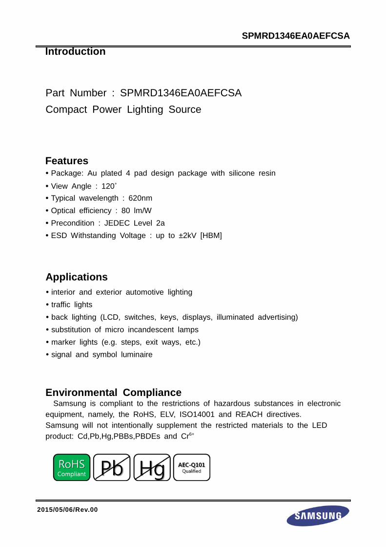
Introduction
Part Number : SPMRD1346EA0AEFCSA
Compact Power Lighting Source
Features
Package: Au plated 4 pad design package with silicone resin
View Angle : 120˚ Typical wavelength : 620nm
Optical efficiency : 80 lm/W
Precondition : JEDEC Level 2a
ESD Withstanding Voltage : up to ±2kV [HBM]
Applications
interior and exterior automotive lighting
traffic lights
back lighting (LCD, switches, keys, displays, illuminated advertising) substitution of micro incandescent lamps
marker lights (e.g. steps, exit ways, etc.) signal and symbol luminaire
Environmental Compliance
Samsung is compliant to the restrictions of hazardous substances in electronic equipment, namely, the RoHS, ELV, ISO14001 and REACH directives. Samsung will not intentionally supplement the restricted materials to the LED product: Cd,Pb,Hg,PBBs,PBDEs and Cr6+

2015/05/06/Rev.00
SPMRD1346EA0AEFCSA
Table of Contents
Part Number Description ------------------------ 3
Characteristic ------------------------ 4
Typical Characteristic ------------------------ 4
Luminous intensity Bin ------------------------ 4
Forward Voltage Bin ------------------------ 5
Dominant Wavelength Bin ------------------------ 5
Absolute Maximum Rating ------------------------ 6
Typical Characteristic Graph ------------------------ 7
Mechanical Dimension ------------------------ 11
Soldering Information ------------------------ 12
Packing Information ------------------------ 13
Product Labeling Information ------------------------ 15
Reliability Test Condition ------------------------ 16
Precaution ------------------------ 17
Revision History ------------------------ 19
Company Information ------------------------ 19

2015/05/06/Rev.00
SPMRD1346EA0AEFCSA
Part Number Description
The Part number designation is explained as follows : SP M RD 1 346 E A 0 AE FC SA
AB C DE F GHI J K L MN OP QR
Where: AB - designates company name and Samsung LED PKG (SP for Samsung LED PKG) C - designates power variant (M for automotive Middle Power) DE - designates color variant (RD for automotive RED and single color) F - designates LED PKG version (value 1 for 1st version up) GHI - designates product configuration and type
J - designates operating condition (value E for 140mA) K - designates specific property
L - designates CRI variant (value 0 for discrete color)
MN - designates forward voltage property
OP - designates dominant wavelength property
QR - designates luminous intensity property

2015/05/06/Rev.00
SPMRD1346EA0AEFCSA
Characteristics
Typical Characteristics
Parameter Symbol Value Unit
Forward voltage (IF = 140mA) VF 2.2 V
Reverse current (VR = 5V) IR 10 ㎂
Peak Wavelength (IF = 140mA) λPeak 629 ㎚
Dominant Wavelength (IF = 140mA) λDom 620 ㎚
Spectral bandwidth at half maximum △λ 16 ㎚
Temperature coefficient of peak
wavelength(IF =140 mA, -30℃≤T≤80℃) TCλPeak 0.13 ㎚/K
Temperature coefficient of dominant
wavelength(IF =140 mA, -30℃≤T≤80℃) TCλDom 0.07 ㎚/K
Temperature coefficient of forward
voltage (IF =140 mA, -30℃≤T≤80℃) TCV -2.26 ㎷/K
Thermal resistance
(Junction to Solder point) Rth_J-S (Elec.) 40 K/W
Luminous Intensity Bin[2]
Symbol Condition Bin Code
Luminous Intensity
IV [cd] Luminous Flux[3]
ΦV [lm]
Min. Max. Min. Max.
IV, ΦV IF = 140mA
EA 7.1 9.0 19 24.0
EB 9.0 11.2 24.0 29.9
* Note
[1] Measurement condition : LED(TJ) = Ambient temperature(TA), by applying pulse current for under 25 ms.
[2] Luminous intensity measuring equipment : CAS140CT
IV and VF tolerances are ±10% and ±0.1 V, respectively.
[3] Luminous flux value is just reference purposes. LED are sorted by the value of luminous intensity
[TJ = 25℃][1]
[TJ = 25℃][1]

2015/05/06/Rev.00
SPMRD1346EA0AEFCSA
• Forward Voltage Bin[2]
Symbol Condition Bin Code Min. Typ. Max. Unit
VF IF = 140mA
E1 1.90 - 2.05
V
E2 2.05 - 2.20
E3 2.20 - 2.35
E4 2.35 - 2.50
• Dominant Wavelength Bin[4]
Symbol Condition Bin Code Min. Typ. Max. Unit
λD IF = 140mA
C1 615.0 - 619.5 nm
C2 619.5 - 624.0
* Note
[4] Wavelength measuring equipment : CAS140CT
tolerance ±2 nm
[TJ = 25℃][1]
[TJ = 25℃][1]

2015/05/06/Rev.00
SPMRD1346EA0AEFCSA
Absolute Maximum Ratings
Parameter Symbol Value Unit
Operating temperature range TOPR -40 ~ 110 ℃
Storage temperature range TSTG -40 ~ 110 ℃
Junction temperature TJ_Max. 125 ℃
Maximum forward current[5]
(TJ : 25℃)[6]
IF 200 mA
Minimum forward current[5]
(TJ : 25℃)[6]
IF 10 mA
Maximum peaked current (TJ : 25℃)[6]
IFM 1000 mA
Reverse voltage
(TJ : 25℃)[6]
VR 5 V
Power consumption
(TJ : 25℃)[6]
PTOT 500 ㎽
ESD sensitivity(HBM) - ±2 kV
* Notes
[5] Unpredictable performance may be resulted by driving the product at below Min. IF or above Max. IF. But there will be no damage to the product.
[6] The measurement condition means that temperature dependence is excluded by applying pulse current for under 25 ms..

2015/05/06/Rev.00
SPMRD1346EA0AEFCSA
Typical Characteristics Graph
Typical Spectrum
: IF = 140 mA, TJ = 25°C[6]
Wavelength Shift vs Angle
: IF = 140 mA, TJ = 25°C[6]

2015/05/06/Rev.00
SPMRD1346EA0AEFCSA
Relative Luminous Intensity & Forward Voltage vs Forward Current : TJ = 25°C[6]
Wavelength Shift vs Forward Current : Reference point_IF = 140 mA, TJ = 25°C[6]

2015/05/06/Rev.00
SPMRD1346EA0AEFCSA
• Relative Luminous Intensity & Forward Voltage vs Temperature
: Reference point_25℃, IF = 140 mA
Wavelength Shift vs Temperature
: Reference point_25℃, IF = 140 mA

2015/05/06/Rev.00
SPMRD1346EA0AEFCSA
Typical Radiant Pattern
: IF = 140mA, Tc = 25°C
Max. Permissible Forward Current
: IF = f (Tc)

2015/05/06/Rev.00
SPMRD1346EA0AEFCSA
Mechanical Dimension[7]
* Note
[7] Unit : mm, Tolerance : ±0.10mm
Do not place pressure on the encapsulating resin (hatch area) The maximum compressing force is 15N on the polymer
• Electric Schematic Diagram
[Top View] [Side View] [Bottom View]
[Front View]
① ②
③ ④
① ②
③ ④
CATHODE MARK
2015/05/06/Rev.00
SPMRD1346EA0AEFCSA
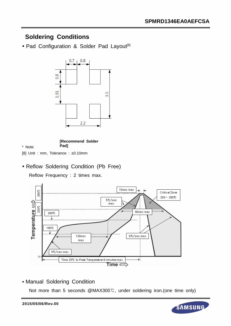
Soldering Conditions
Pad Configuration & Solder Pad Layout[8]
* Note
[8] Unit : mm, Tolerance : ±0.10mm
Reflow Soldering Condition (Pb Free) Reflow Frequency : 2 times max.
Manual Soldering Condition
Not more than 5 seconds @MAX300℃, under soldering iron.(one time only)
[Recommend Solder Pad]
2015/05/06/Rev.00
SPMRD1346EA0AEFCSA
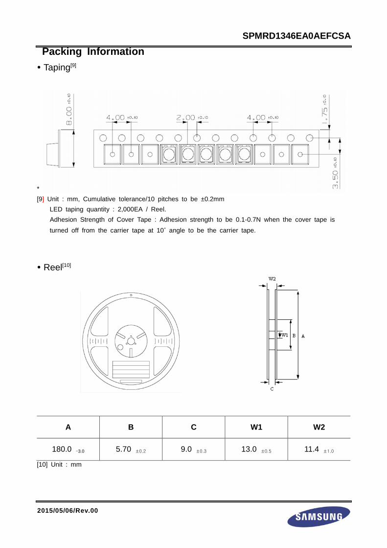
Packing Information
Taping[9]
* Note
[9] Unit : mm, Cumulative tolerance/10 pitches to be ±0.2mm
LED taping quantity : 2,000EA / Reel. Adhesion Strength of Cover Tape : Adhesion strength to be 0.1-0.7N when the cover tape is
turned off from the carrier tape at 10˚ angle to be the carrier tape.
Reel[10]
A B C W1 W2
180.0 -3.0 5.70 ±0.2 9.0 ±0.3
13.0 ±0.5 11.4 ±1.0
[10] Unit : mm

2015/05/06/Rev.00
SPMRD1346EA0AEFCSA
• Packing Box information
Dimension of Transportation Box in mm
Width Length Height Reels/box
245 220 182 Up to 10 Reels
245 220 86 Up to 5 Reels

2015/05/06/Rev.00
SPMRD1346EA0AEFCSA
Product Labeling Information
Label Information
1. Bin Code
AB : Forward Voltage(VF) Bin
CD : Dominant Wavelength(λD) Bin
EF : Luminous Intensity(IV) Bin
2. Lot No.
①②③④⑤⑥⑦⑧⑨ / 1ⓐⓑⓒ / 2,000 PCS
① : Production Site (S:SAMSUNG KOREA, G:TIANJIN CHINA)
② : L (LED)
③ : Product State (A:Normality, B:Bulk, C:First Production, R:Reproduction,
S:Sample) ④ : Year (X:2013, Y:2014, Z:2015 ...)
⑤ : Month (1 ~ 9, A, B, C)
⑥ : Day (1 ~ 9, A, B ~ V)
⑦⑧⑨ : SAMSUNG ELECTRONICS Product number (1 ~ 999)
ⓐⓑⓒ : Reel Number (1 ~ 999)
ABCDEF SPMRD1346EA0 ABCDEF XXXX IIIIIIIIIIIIIIIIIIIIIIIIIIII ①②③④⑤⑥⑦⑧⑨ / 1ⓐⓑⓒ / 1,000 PCS IIIIIIIIIIIIIIIIIIIIIIIII
Bin Code
Part Number
Lot Number

2015/05/06/Rev.00
SPMRD1346EA0AEFCSA
Reliability Test Conditions
For detailed Information please contact your SAMSUNG Sales partner

2015/05/06/Rev.00
SPMRD1346EA0AEFCSA
Precaution for Use
1) For over-current-proof function, customers are recommended to apply resistors to
prevent sudden change of the current caused by slight shift of the voltage.
2) This device should not be used in any type of fluid such as water, oil, organic
solvent, etc. When washing is required, IPA is recommended to use. 3) When the LEDs illuminate, operating current should be decided after considering the
ambient maximum temperature. 4) LEDs must be stored in a clean environment. If the LEDs are to be stored for 3 months or more after being shipped from
Samsung Electronics, they should be packed by a sealed container with nitrogen gas
injected.(Shelf life of sealed bags: 12 months, temp. ~40 ℃, ~90 % RH)
5) After storage bag is open, device subjected to soldering, solder reflow, or other high temperature processes must be: a. Mounted within 672 hours (28 days) at an assembly line with a condition of no
more than 30 ℃/60 %RH,
b. Stored at <10 %RH. 6) Repack unused Products with anti-moisture packing, fold to close any opening and
then store in a dry place.
7) Devices require baking before mounting, if humidity card reading is >60 %
at 23±5 ℃.
8) Devices must be baked for 1 hour at 65±5 ℃, if baking is required.
9) The LEDs are sensitive to the static electricity and surge. It is recommended to
use a wrist band or anti-electrostatic glove when handling the LEDs.
If voltage exceeding the absolute maximum rating is applied to LEDs, it may cause
damage or even destruction to LED devices.
Damaged LEDs may show some unusual characteristics such as increase in leak
current, lowered turn-on voltage, or abnormal lighting of LEDs at low current.

2015/05/06/Rev.00
SPMRD1346EA0AEFCSA
10) VOCs (volatile organic compounds) may be occurred by adhesives, flux, hardener or
organic additives which is used in luminaires (fixture) and LED silicone bags are
permeable to it. It may lead a discoloration when LED expose to heat or light. This phenomenon can give a significant loss of light emitted (output) from the
luminaires (fixtures). In order to prevent these problems, we recommend you to know the physical
properties for the materials used in luminaires, It requires to select carefully.

2015/05/06/Rev.00
SPMRD1346EA0AEFCSA
Revision History
Date Revision History Author
Drawn Approved
2015.05.06 Initial Edition
S.Y. GO S.B. Kwak
Company Information
Copyright @1995-2015 All rights reserved
Samsung Electronics
95, Samsung 2-ro, Giheung-Gu,,
Yongin-City, Gyeonggi-Do 446-711 Korea
http://www.samsung.com/sec/business/#
Sales Contact : [email protected]
US Samsung Semiconductor Inc., 3655 N. First Street, San Jose CA 95134, USA TEL. +1-408-544-4000
Europe Samsung Electronics Germany GmbH, Samsung House, Am Kronberger Hang 6, Schwalbach/Ts,Germany TEL. +49-6196-66-0
Japan Samsung Japan Corporation SLED Team 10F, Shinagawa Grand Central Tower 2-16-4, Kounan, Minato-ku, Tokyo 108-8240, Japan TEL. +81-3-6369-6327
China (Tianjin Office in China) Tianjin Samsung LED Co., LTD. Weisi (6th) Rd., Micro-Electronics Industrial Park, Xiqing District, Tianjin 300385, China TEL. +86-755-8608-5550