
Data Path and Control - University of California, Santa...
90
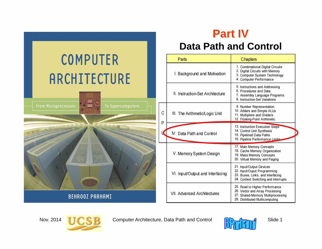
Nov. 2014 Computer Architecture, Data Path and Control Slide 1 Part IV Data Path and Control
Transcript of Data Path and Control - University of California, Santa...
Nov. 2014 Computer Architecture, Data Path and Control Slide 1
Part IVData Path and Control
Nov. 2014 Computer Architecture, Data Path and Control Slide 2
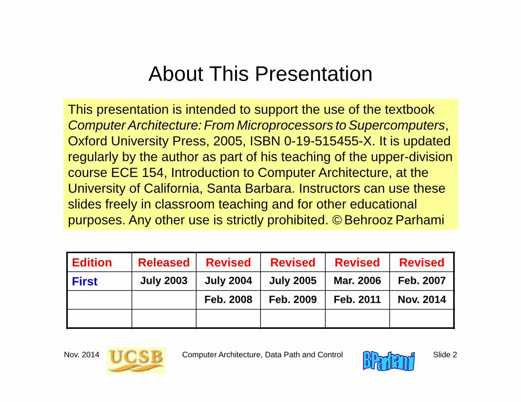
About This PresentationThis presentation is intended to support the use of the textbook Computer Architecture: From Microprocessors to Supercomputers, Oxford University Press, 2005, ISBN 0-19-515455-X. It is updated regularly by the author as part of his teaching of the upper-division course ECE 154, Introduction to Computer Architecture, at the University of California, Santa Barbara. Instructors can use these slides freely in classroom teaching and for other educational purposes. Any other use is strictly prohibited. © Behrooz Parhami
Edition Released Revised Revised Revised RevisedFirst July 2003 July 2004 July 2005 Mar. 2006 Feb. 2007
Feb. 2008 Feb. 2009 Feb. 2011 Nov. 2014
Nov. 2014 Computer Architecture, Data Path and Control Slide 3
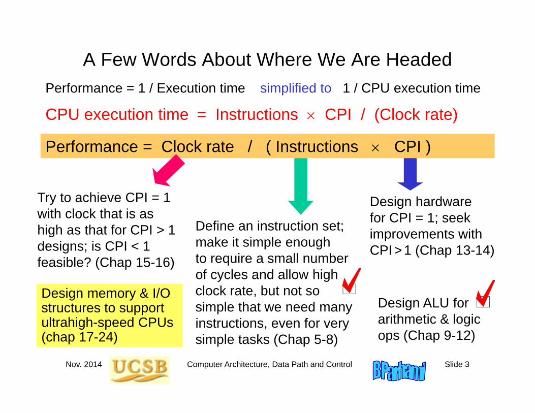
A Few Words About Where We Are HeadedPerformance = 1 / Execution time simplified to 1 / CPU execution time
CPU execution time = Instructions CPI / (Clock rate)
Performance = Clock rate / ( Instructions CPI )
Define an instruction set;make it simple enough to require a small number of cycles and allow high clock rate, but not so simple that we need many instructions, even for very simple tasks (Chap 5-8)
Design hardware for CPI = 1; seek improvements with CPI >1 (Chap 13-14)
Design ALU for arithmetic & logic ops (Chap 9-12)
Try to achieve CPI = 1 with clock that is as high as that for CPI > 1 designs; is CPI < 1 feasible? (Chap 15-16)
Design memory & I/O structures to support ultrahigh-speed CPUs(chap 17-24)
Nov. 2014 Computer Architecture, Data Path and Control Slide 4
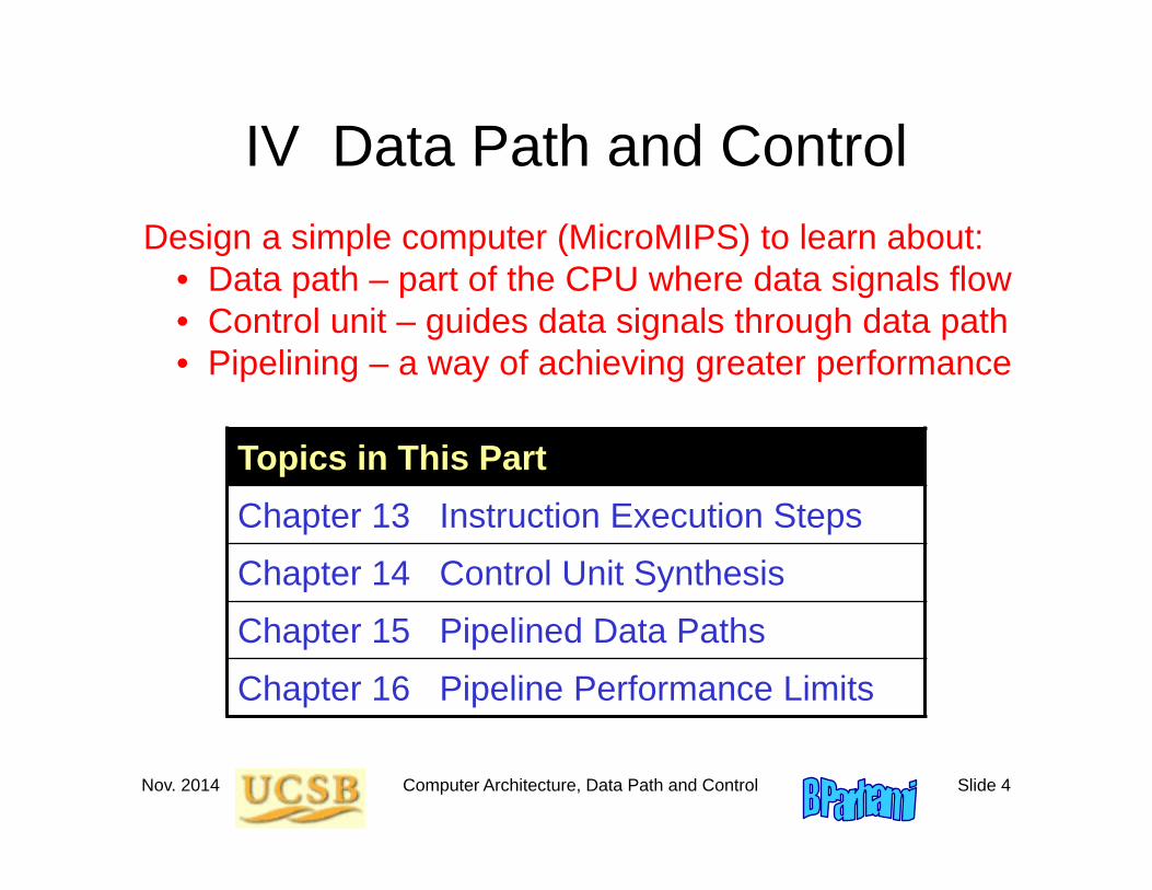
IV Data Path and Control
Topics in This PartChapter 13 Instruction Execution StepsChapter 14 Control Unit SynthesisChapter 15 Pipelined Data PathsChapter 16 Pipeline Performance Limits
Design a simple computer (MicroMIPS) to learn about:• Data path – part of the CPU where data signals flow• Control unit – guides data signals through data path• Pipelining – a way of achieving greater performance
Nov. 2014 Computer Architecture, Data Path and Control Slide 5
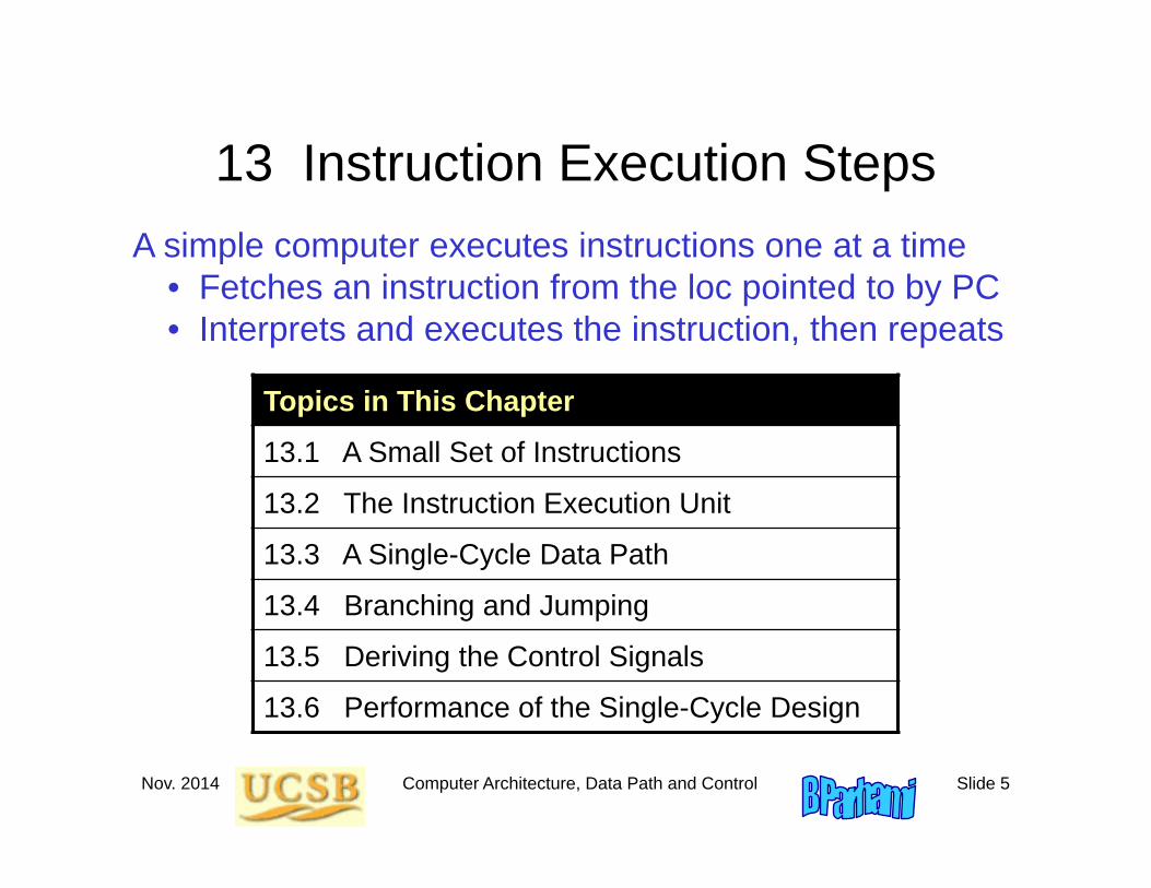
13 Instruction Execution StepsA simple computer executes instructions one at a time
• Fetches an instruction from the loc pointed to by PC• Interprets and executes the instruction, then repeats
Topics in This Chapter
13.1 A Small Set of Instructions
13.2 The Instruction Execution Unit
13.3 A Single-Cycle Data Path
13.4 Branching and Jumping
13.5 Deriving the Control Signals
13.6 Performance of the Single-Cycle Design
Nov. 2014 Computer Architecture, Data Path and Control Slide 6
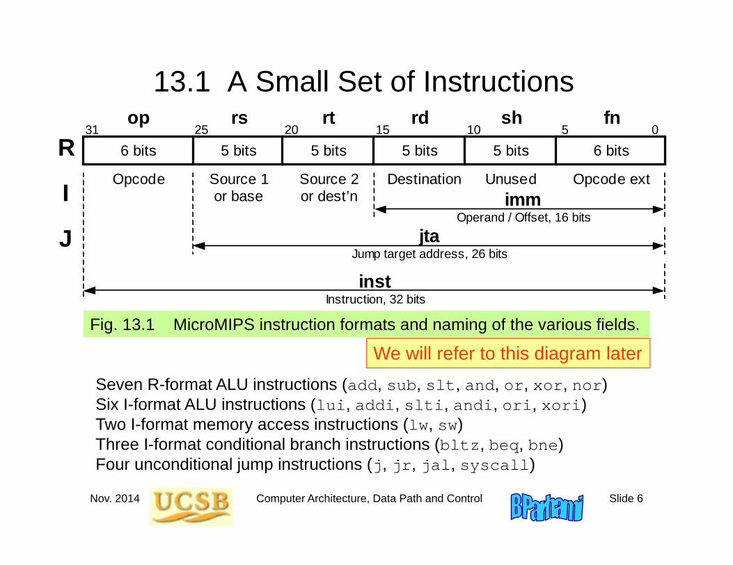
13.1 A Small Set of Instructions
Fig. 13.1 MicroMIPS instruction formats and naming of the various fields.
5 bits 5 bits 31 25 20 15 0
Opcode Source 1 or base
Source 2 or dest’n
op rs rt
R 6 bits 5 bits
rd
5 bits
sh
6 bits 10 5
fn
jta Jump target address, 26 bits
imm Operand / Offset, 16 bits
Destination Unused Opcode ext I
J inst
Instruction, 32 bits
Seven R-format ALU instructions (add, sub, slt, and, or, xor, nor)Six I-format ALU instructions (lui, addi, slti, andi, ori, xori)Two I-format memory access instructions (lw, sw)Three I-format conditional branch instructions (bltz, beq, bne)Four unconditional jump instructions (j, jr, jal, syscall)
We will refer to this diagram later
Nov. 2014 Computer Architecture, Data Path and Control Slide 7
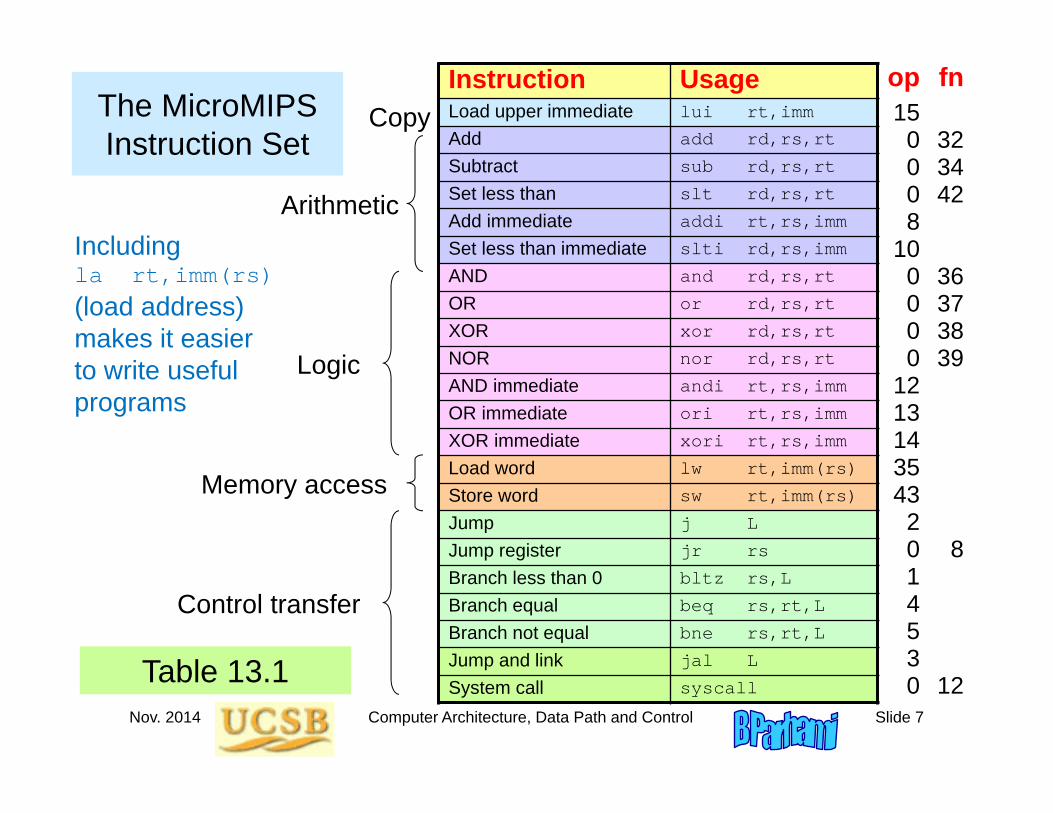
The MicroMIPS Instruction Set
Instruction UsageLoad upper immediate lui rt,imm
Add add rd,rs,rt
Subtract sub rd,rs,rt
Set less than slt rd,rs,rt
Add immediate addi rt,rs,imm
Set less than immediate slti rd,rs,imm
AND and rd,rs,rt
OR or rd,rs,rt
XOR xor rd,rs,rt
NOR nor rd,rs,rt
AND immediate andi rt,rs,imm
OR immediate ori rt,rs,imm
XOR immediate xori rt,rs,imm
Load word lw rt,imm(rs)
Store word sw rt,imm(rs)
Jump j L
Jump register jr rs
Branch less than 0 bltz rs,L
Branch equal beq rs,rt,L
Branch not equal bne rs,rt,L
Jump and link jal L
System call syscall
Copy
Control transfer
Logic
Arithmetic
Memory access
op15
0008
100000
1213143543
2014530
fn
323442
36373839
8
12Table 13.1
Including la rt,imm(rs)(load address)makes it easierto write usefulprograms

Nov. 2014 Computer Architecture, Data Path and Control Slide 8
13.2 The Instruction Execution Unit
Fig. 13.2 Abstract view of the instruction execution unit for MicroMIPS. For naming of instruction fields, see Fig. 13.1.
ALU
Data cache
Instr cache
Next addr
Control
Reg file
op
jta
fn
inst
imm
rs,rt,rd (rs)
(rt)
Address Data
PC
5 bits 5 bits 31 25 20 15 0
Opcode Source 1 or base
Source 2 or dest’n
op rs rt
R 6 bits 5 bits
rd
5 bits
sh
6 bits 10 5
fn
jta Jump target address, 26 bits
imm Operand / Offset, 16 bits
Destination Unused Opcode ext I
J inst
Instruction, 32 bits
bltz,jr
beq,bne
12 A/L, lui, lw,sw
j,jal
syscall
22 instructions
Harvardarchitecture
Nov. 2014 Computer Architecture, Data Path and Control Slide 9
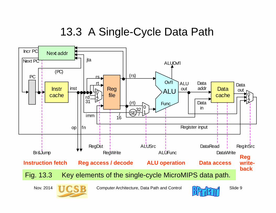
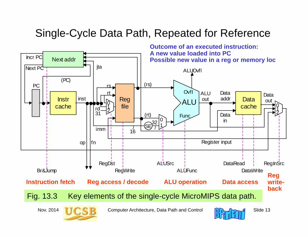
13.3 A Single-Cycle Data Path
Fig. 13.3 Key elements of the single-cycle MicroMIPS data path.
/
ALU
Data cache
Instr cache
Next addr
Reg file
op
jta
fn
inst
imm
rs (rs)
(rt)
Data addr
Data in 0
1
ALUSrc ALUFunc DataWrite
DataRead
SE
RegInSrc
rt
rd
RegDst RegWrite
32 / 16
Register input
Data out
Func
ALUOvfl
Ovfl
31
0 1 2
Next PC
Incr PC
(PC)
Br&Jump
ALU out
PC
0 1 2
Instruction fetch Reg access / decode ALU operation Data accessRegwrite-back
Nov. 2014 Computer Architecture, Data Path and Control Slide 10
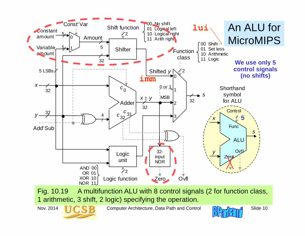
An ALU for MicroMIPS
Fig. 10.19 A multifunction ALU with 8 control signals (2 for function class, 1 arithmetic, 3 shift, 2 logic) specifying the operation.
AddSub
x y
y
x
Adder
c 32
c 0
k /
Shifter
Logic unit
s
Logic function
Amount
5
2
Constant amount
Variable amount
5
5
ConstVar
0
1
0
1
2
3
Function class
2
Shift function
5 LSBs Shifted y
32
32
32
2
c 31
32-input NOR
Ovfl Zero
32 32
MSB
ALU
y
x
s
Shorthand symbol for ALU
Ovfl Zero
Func
Control
0 or 1
AND 00 OR 01
XOR 10 NOR 11
00 Shift 01 Set less 10 Arithmetic 11 Logic
00 No shift 01 Logical left 10 Logical right 11 Arith right
lui
imm
We use only 5 control signals
(no shifts)
5

Nov. 2014 Computer Architecture, Data Path and Control Slide 11
13.4 Branching and Jumping
Fig. 13.4 Next-address logic for MicroMIPS (see top part of Fig. 13.3). Adder
jta imm
(rs)
(rt)
SE
SysCallAddr
PCSrc
(PC)
Branch condition checker
in c
1 0 1 2 3
/ 30
/ 32 BrTrue / 32
/ 30 / 30
/ 30
/ 30
/ 30
/ 30 / 26
/ 30
/ 30 4 MSBs
30 MSBs
BrType
IncrPC
NextPC
/ 30 31:2
16
(PC)31:2 + 1 Default option(PC)31:2 + 1 + imm When instruction is branch and condition is met(PC)31:28 | jta When instruction is j or jal(rs)31:2 When the instruction is jrSysCallAddr Start address of an operating system routine
Update options for PC
Lowest 2 bits of PC always 00
4 MSBs
Nov. 2014 Computer Architecture, Data Path and Control Slide 12
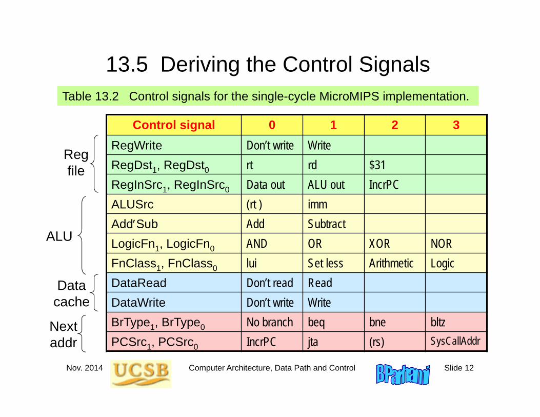
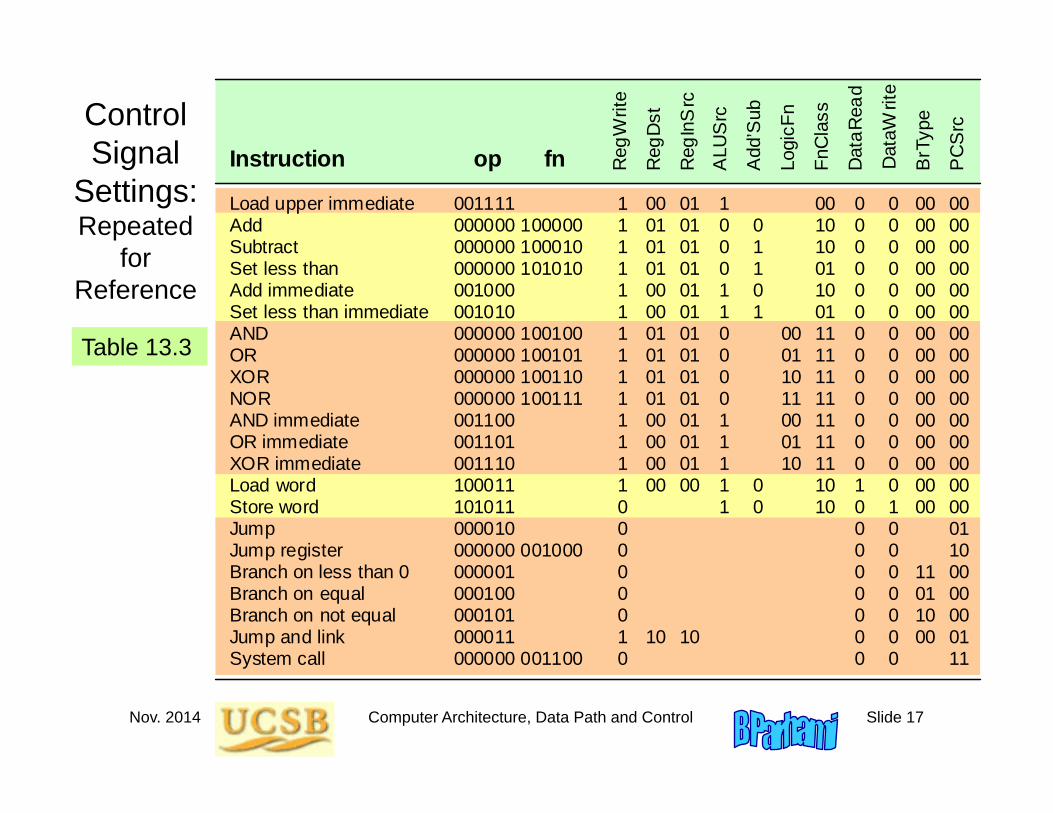
13.5 Deriving the Control SignalsTable 13.2 Control signals for the single-cycle MicroMIPS implementation.
Control signal 0 1 2 3RegWrite Don’t write WriteRegDst1, RegDst0 rt rd $31RegInSrc1, RegInSrc0 Data out ALU out IncrPCALUSrc (rt ) immAddSub Add SubtractLogicFn1, LogicFn0 AND OR XOR NORFnClass1, FnClass0 lui Set less Arithmetic LogicDataRead Don’t read ReadDataWrite Don’t write WriteBrType1, BrType0 No branch beq bne bltzPCSrc1, PCSrc0 IncrPC jta (rs) SysCallAddr
Reg file
Data cache
Next addr
ALU
Nov. 2014 Computer Architecture, Data Path and Control Slide 13
Single-Cycle Data Path, Repeated for Reference
Fig. 13.3 Key elements of the single-cycle MicroMIPS data path.
/
ALU
Data cache
Instr cache
Next addr
Reg file
op
jta
fn
inst
imm
rs (rs)
(rt)
Data addr
Data in 0
1
ALUSrc ALUFunc DataWrite
DataRead
SE
RegInSrc
rt
rd
RegDst RegWrite
32 / 16
Register input
Data out
Func
ALUOvfl
Ovfl
31
0 1 2
Next PC
Incr PC
(PC)
Br&Jump
ALU out
PC
0 1 2
Outcome of an executed instruction:A new value loaded into PCPossible new value in a reg or memory loc
Instruction fetch Reg access / decode ALU operation Data accessRegwrite-back
Nov. 2014 Computer Architecture, Data Path and Control Slide 14
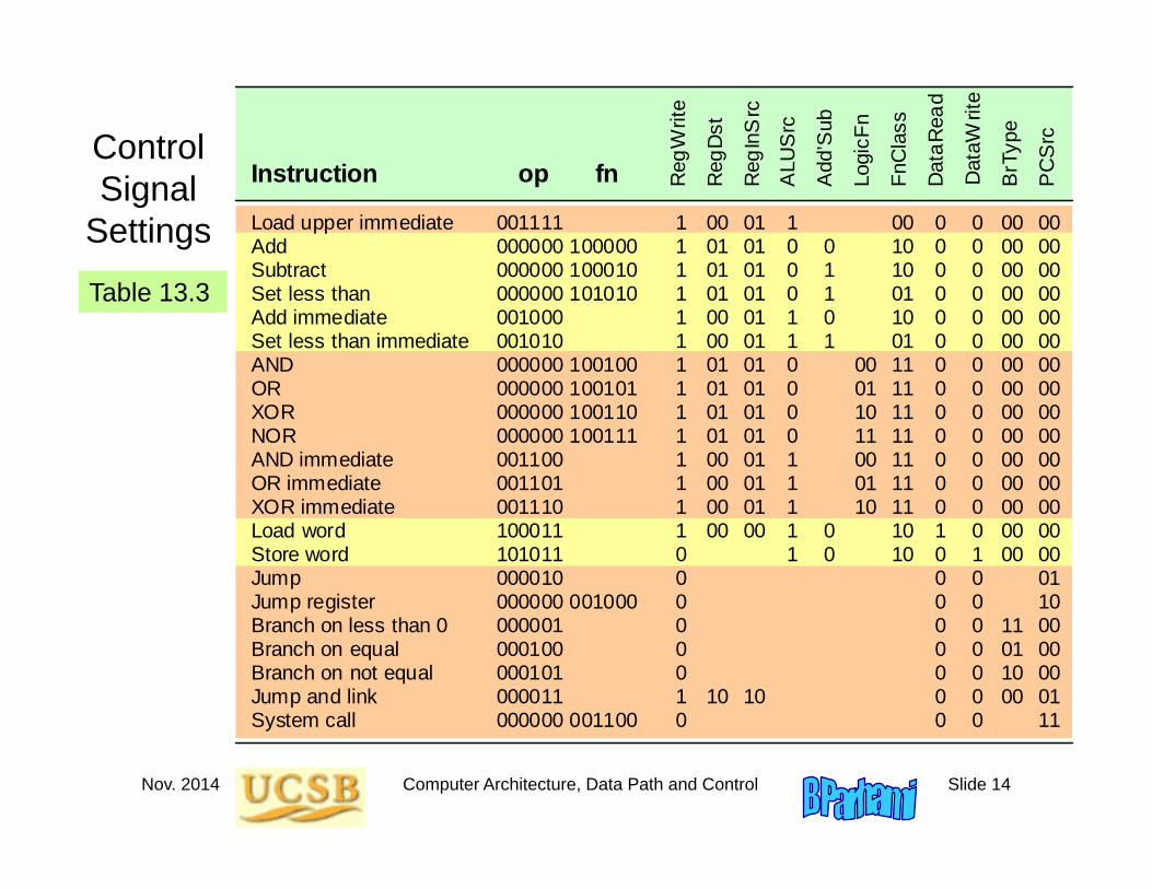
Control Signal
Settings
Table 13.3
Load upper immediate Add Subtract Set less than Add immediate Set less than immediate AND OR XOR NOR AND immediate OR immediate XOR immediate Load word Store word Jump Jump register Branch on less than 0 Branch on equal Branch on not equal Jump and link System call
001111 000000 100000 000000 100010 000000 101010 001000 001010 000000 100100 000000 100101 000000 100110 000000 100111 001100 001101 001110 100011 101011 000010 000000 001000 000001 000100 000101 000011 000000 001100
1 1 1 1 1 1 1 1 1 1 1 1 1 1 0 0 0 0 0 0 1 0
op fn
00 01 01 01 00 00 01 01 01 01 00 00 00 00
10
01 01 01 01 01 01 01 01 01 01 01 01 01 00
10
1 0 0 0 1 1 0 0 0 0 1 1 1 1 1
0 1 1 0 1 0 0
00 01 10 11 00 01 10
00 10 10 01 10 01 11 11 11 11 11 11 11 10 10
0 0 0 0 0 0 0 0 0 0 0 0 0 1 0 0 0 0 0 0 0 0
0 0 0 0 0 0 0 0 0 0 0 0 0 0 1 0 0 0 0 0 0 0
00 00 00 00 00 00 00 00 00 00 00 00 00 00 00
11 0110 00
00 00 00 00 00 00 00 00 00 00 00 00 00 00 00 01 10 00 00 00 01 11
Instruction Reg
Writ
e
Reg
Dst
Reg
InS
rc
ALU
Src
Add
’Sub
Logi
cFn
FnC
lass
Dat
aRea
d
Dat
aWrit
e
BrT
ype
PC
Src
Nov. 2014 Computer Architecture, Data Path and Control Slide 15
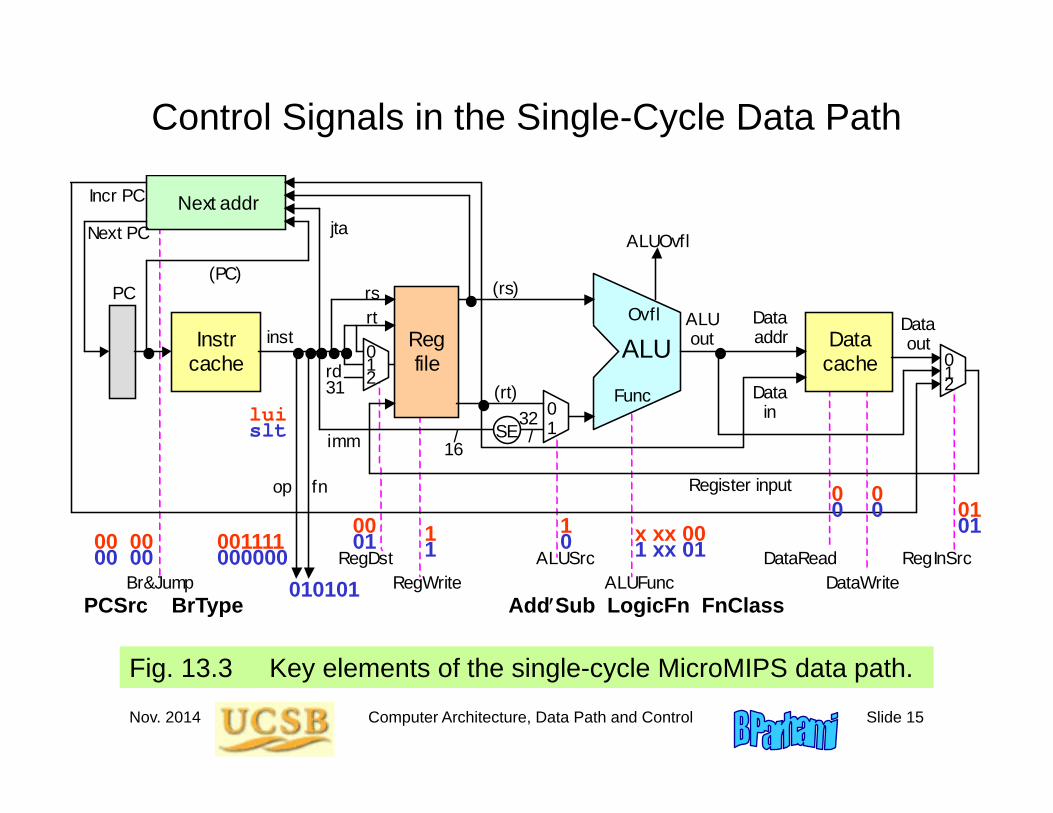
Control Signals in the Single-Cycle Data Path
Fig. 13.3 Key elements of the single-cycle MicroMIPS data path.
/
ALU
Data cache
Instr cache
Next addr
Reg file
op
jta
fn
inst
imm
rs (rs)
(rt)
Data addr
Data in 0
1
ALUSrc ALUFunc DataWrite
DataRead
SE
RegInSrc
rt
rd
RegDst RegWrite
32 / 16
Register input
Data out
Func
ALUOvfl
Ovfl
31
0 1 2
Next PC
Incr PC
(PC)
Br&Jump
ALU out
PC
0 1 2
AddSub LogicFn FnClassPCSrc BrType
lui
001111 10001
1 x xx 00
0 0
00 00
slt
000000 10101
0 1 xx 01
0 0
00 00010101
Nov. 2014 Computer Architecture, Data Path and Control Slide 16
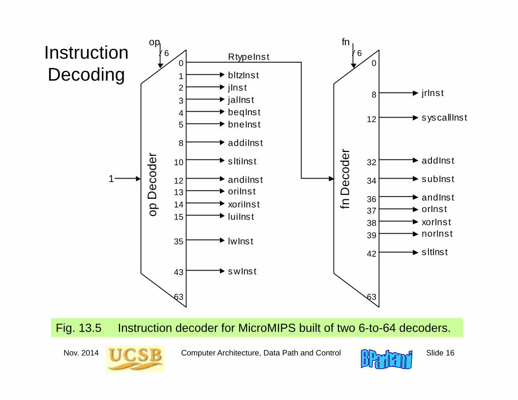
Instruction Decoding
Fig. 13.5 Instruction decoder for MicroMIPS built of two 6-to-64 decoders.
jrIns t
norInst
s ltIns t
orIns t xorInst
syscallIns t
andInst
addInst
subInst
RtypeInst
bltzIns t jIns t jalIns t beqInst bneInst
s ltiIns t
andiIns t oriIns t xoriIns t luiIns t
lwInst
swInst
addiIns t
1
0 1 2 3 4 5
10
12 13 14 15
35
43
63
8 op
Dec
oder
fn D
ecod
er
/ 6 / 6 op fn
0
8
12
32
34
36 37 38 39
42
63
Nov. 2014 Computer Architecture, Data Path and Control Slide 17
Control Signal
Settings:Repeated
for Reference
Table 13.3
Load upper immediate Add Subtract Set less than Add immediate Set less than immediate AND OR XOR NOR AND immediate OR immediate XOR immediate Load word Store word Jump Jump register Branch on less than 0 Branch on equal Branch on not equal Jump and link System call
001111 000000 100000 000000 100010 000000 101010 001000 001010 000000 100100 000000 100101 000000 100110 000000 100111 001100 001101 001110 100011 101011 000010 000000 001000 000001 000100 000101 000011 000000 001100
1 1 1 1 1 1 1 1 1 1 1 1 1 1 0 0 0 0 0 0 1 0
op fn
00 01 01 01 00 00 01 01 01 01 00 00 00 00
10
01 01 01 01 01 01 01 01 01 01 01 01 01 00
10
1 0 0 0 1 1 0 0 0 0 1 1 1 1 1
0 1 1 0 1 0 0
00 01 10 11 00 01 10
00 10 10 01 10 01 11 11 11 11 11 11 11 10 10
0 0 0 0 0 0 0 0 0 0 0 0 0 1 0 0 0 0 0 0 0 0
0 0 0 0 0 0 0 0 0 0 0 0 0 0 1 0 0 0 0 0 0 0
00 00 00 00 00 00 00 00 00 00 00 00 00 00 00
11 0110 00
00 00 00 00 00 00 00 00 00 00 00 00 00 00 00 01 10 00 00 00 01 11
Instruction Reg
Writ
e
Reg
Dst
Reg
InS
rc
ALU
Src
Add
’Sub
Logi
cFn
FnC
lass
Dat
aRea
d
Dat
aWrit
e
BrT
ype
PC
Src

Nov. 2014 Computer Architecture, Data Path and Control Slide 18
Control Signal Generation
Auxiliary signals identifying instruction classes
arithInst = addInst subInst sltInst addiInst sltiInst
logicInst = andInst orInst xorInst norInst andiInst oriInst xoriInst
immInst = luiInst addiInst sltiInst andiInst oriInst xoriInst
Example logic expressions for control signals
RegWrite = luiInst arithInst logicInst lwInst jalInst
ALUSrc = immInst lwInst swInst
AddSub = subInst sltInst sltiInst
DataRead = lwInst
PCSrc0 = jInst jalInst syscallInst
Control
addInstsubInst
jInst
sltInst
.
..
.
..
Nov. 2014 Computer Architecture, Data Path and Control Slide 19
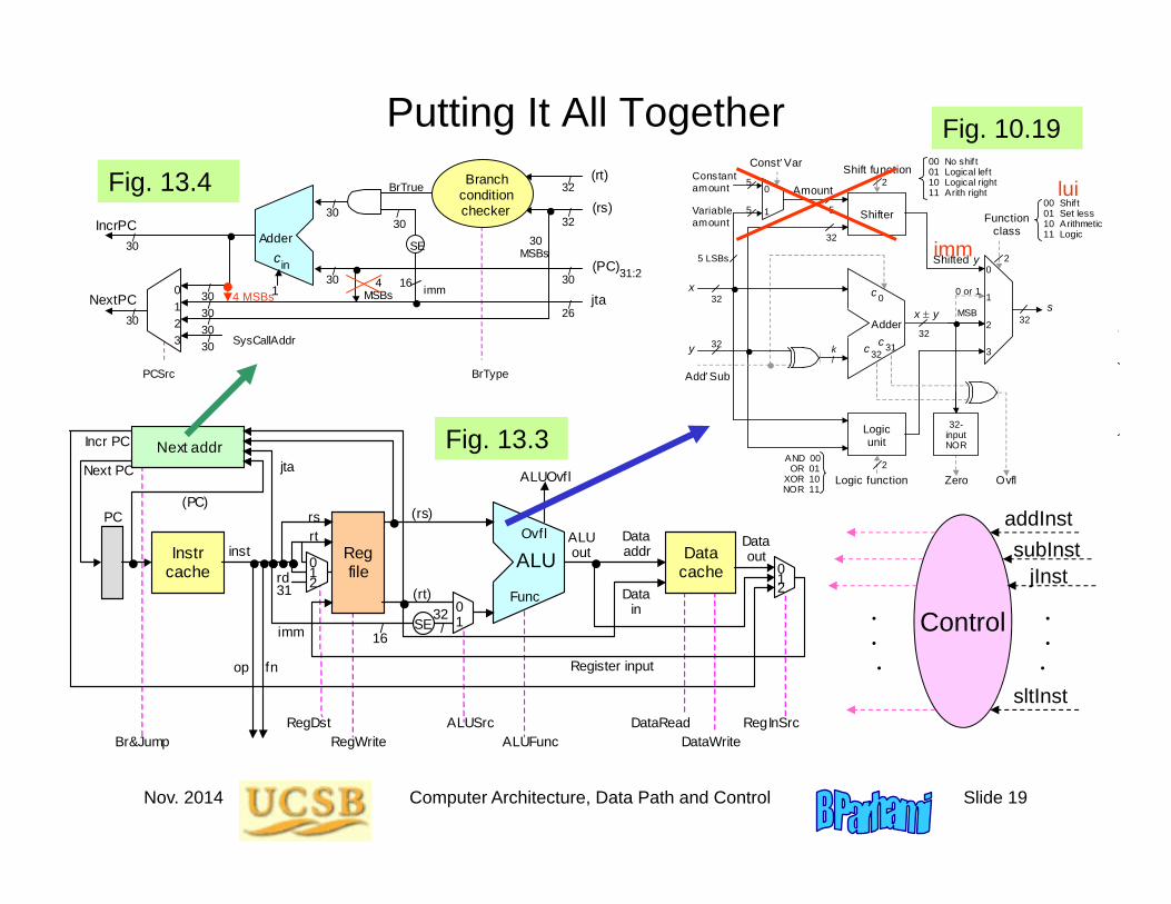
Putting It All Together
/
ALU
Data cache
Instr cache
Next addr
Reg file
op
jta
fn
inst
imm
rs (rs)
(rt)
Data addr
Data in 0
1
ALUSrc ALUFunc DataWrite
DataRead
SE
RegInSrc
rt
rd
RegDst RegWrite
32 / 16
Register input
Data out
Func
ALUOvfl
Ovfl
31
0 1 2
Next PC
Incr PC
(PC)
Br&Jump
ALU out
PC
0 1 2
Fig. 13.3
Control
addInstsubInst
jInst
sltInst
.
..
.
..
Fig. 10.19
AddSub
x y
y
x
Adder
c 32
c 0
k /
Shifter
Logic unit
s
Logic function
Amount
5
2
Constant amount
Variable amount
5
5
ConstVar
0
1
0
1
2
3
Function class
2
Shift function
5 LSBs Shifted y
32
32
32
2
c 31
32-input NOR
Ovfl Zero
32 32
MSB
A
y
x
Shorthsymbfor AL
OZero
Fun
Cont
0 or 1
AND 00 OR 01
XOR 10 NOR 11
00 Shif t 01 Set less 10 Arithmetic 11 Logic
00 No shif t 01 Logical lef t 10 Logical right 11 Arith right
imm
lui
Adder
jta imm
(rs)
(rt)
SE
SysCallAddr
PCSrc
(PC)
Branch condition checker
in c
1 0 1 2 3
/ 30
/ 32 BrTrue / 32
/ 30 / 30
/ 30
/ 30
/ 30
/ 30 / 26
/ 30
/ 30 4 MSBs
30 MSBs
BrType
IncrPC
NextPC
/ 30 31:2
16
Fig. 13.4
4 MSBs
Nov. 2014 Computer Architecture, Data Path and Control Slide 20
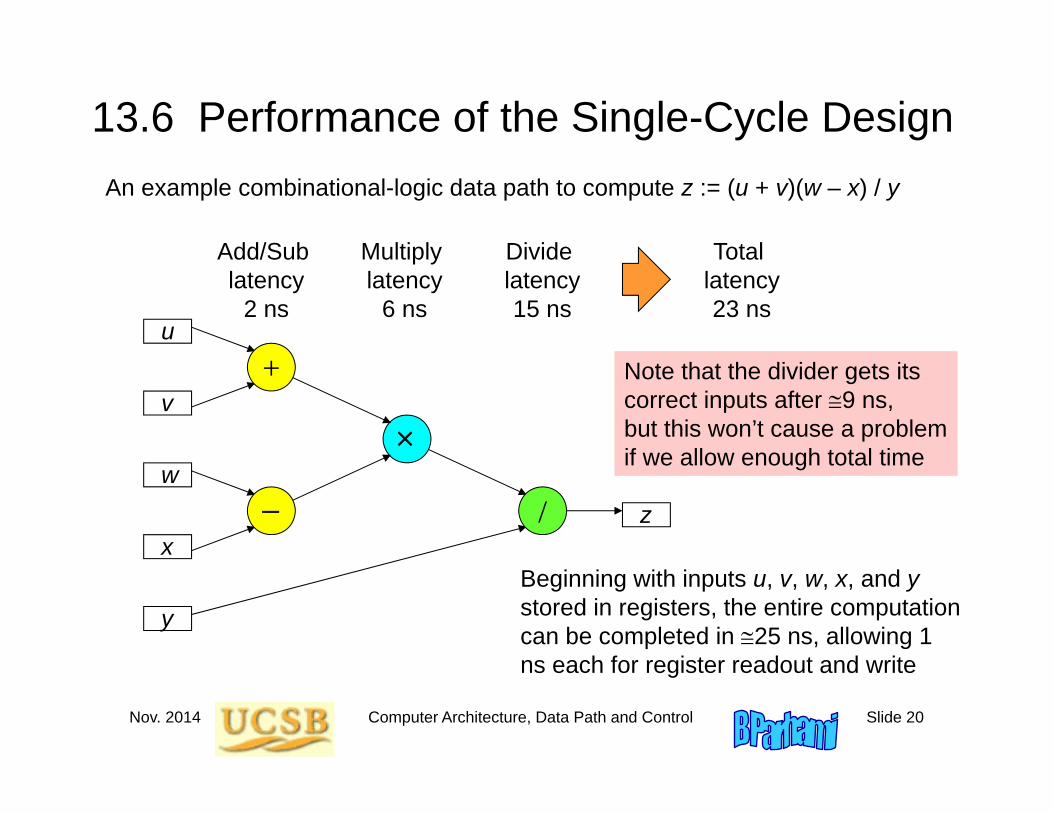
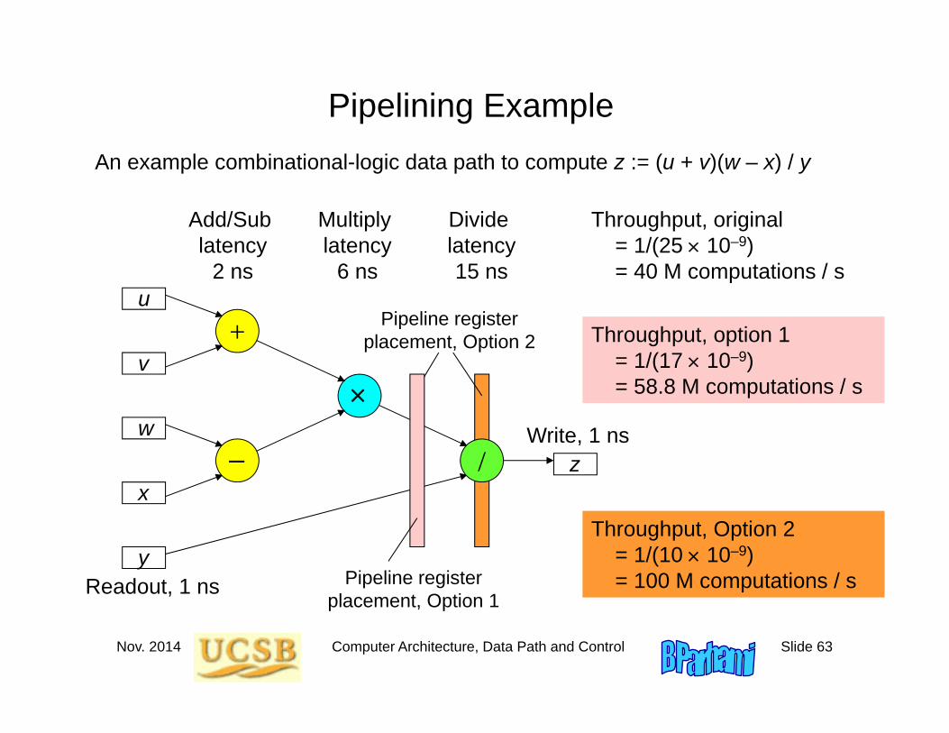
13.6 Performance of the Single-Cycle DesignAn example combinational-logic data path to compute z := (u + v)(w – x) / y
Add/Sub latency
2 ns
Multiply latency
6 ns
Divide latency15 ns
Beginning with inputs u, v, w, x, and y stored in registers, the entire computation can be completed in 25 ns, allowing 1 ns each for register readout and write
Total latency23 ns
Note that the divider gets its correct inputs after 9 ns, but this won’t cause a problem if we allow enough total time
/
+
y
u
v
w
xz
Nov. 2014 Computer Architecture, Data Path and Control Slide 21
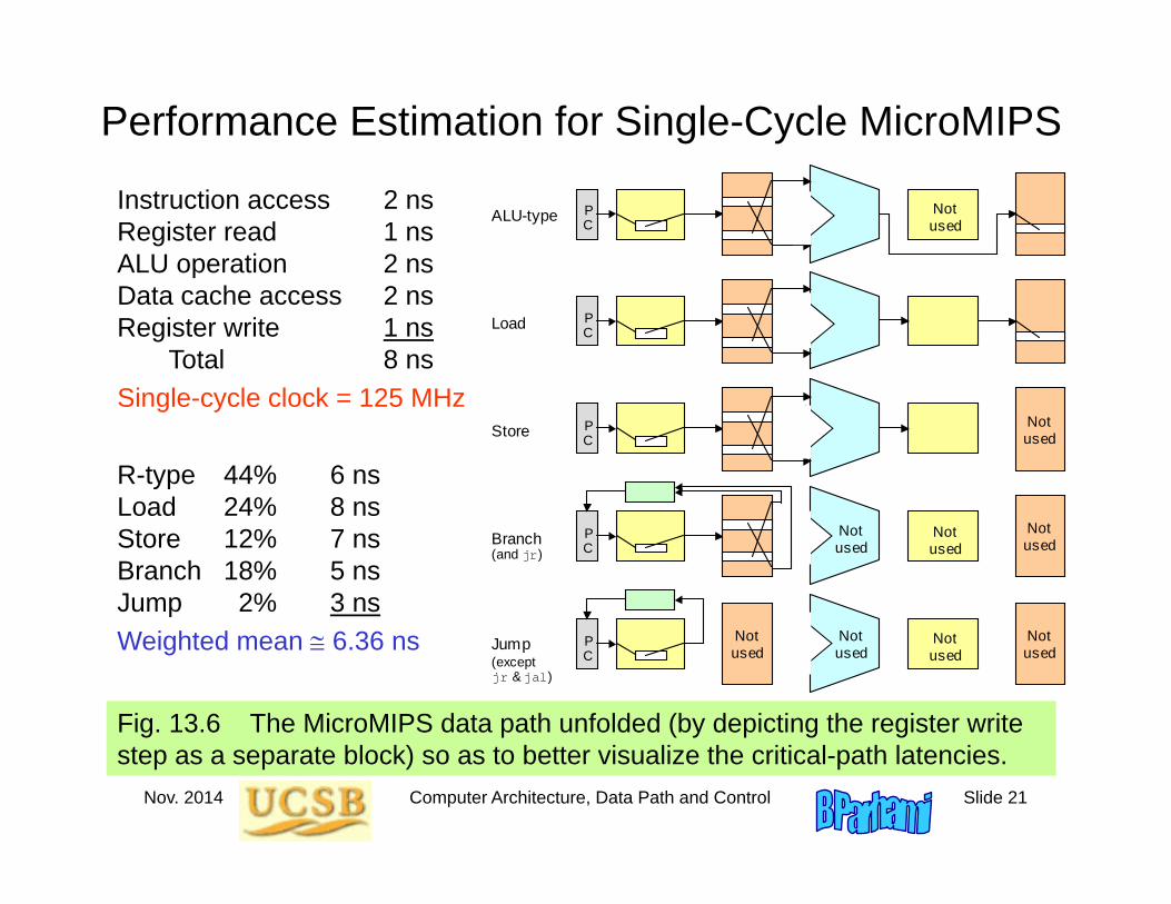
Performance Estimation for Single-Cycle MicroMIPS
Fig. 13.6 The MicroMIPS data path unfolded (by depicting the register write step as a separate block) so as to better visualize the critical-path latencies.
Instruction access 2 nsRegister read 1 nsALU operation 2 nsData cache access 2 nsRegister write 1 ns
Total 8 nsSingle-cycle clock = 125 MHz
P C
P C
P C
P C
P C
ALU-type
Load
Store
Branch
Jump
Not used
Not used
Not used
Not used
Not used
Not used
Not used
Not used
Not used
(and jr)
(except jr & jal)
R-type 44% 6 nsLoad 24% 8 nsStore 12% 7 nsBranch 18% 5 nsJump 2% 3 nsWeighted mean 6.36 ns

Nov. 2014 Computer Architecture, Data Path and Control Slide 22
How Good is Our Single-Cycle Design?
Instruction access 2 nsRegister read 1 nsALU operation 2 nsData cache access 2 nsRegister write 1 ns
Total 8 nsSingle-cycle clock = 125 MHz
Clock rate of 125 MHz not impressive
How does this compare with current processors on the market?
Not bad, where latency is concerned
A 2.5 GHz processor with 20 or so pipeline stages has a latency of about
0.4 ns/cycle 20 cycles = 8 ns
Throughput, however, is much better for the pipelined processor:
Up to 20 times better with single issue
Perhaps up to 100 times better with multiple issue
Nov. 2014 Computer Architecture, Data Path and Control Slide 23
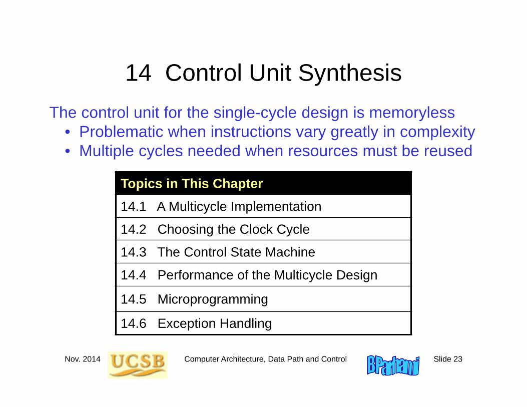
14 Control Unit SynthesisThe control unit for the single-cycle design is memoryless
• Problematic when instructions vary greatly in complexity• Multiple cycles needed when resources must be reused
Topics in This Chapter14.1 A Multicycle Implementation
14.2 Choosing the Clock Cycle
14.3 The Control State Machine
14.4 Performance of the Multicycle Design
14.5 Microprogramming
14.6 Exception Handling

Nov. 2014 Computer Architecture, Data Path and Control Slide 24
14.1 A Multicycle Implementation
Appointment book for a dentist
Assume longest treatment takes one hour
Single-cycle Multicycle
Nov. 2014 Computer Architecture, Data Path and Control Slide 25
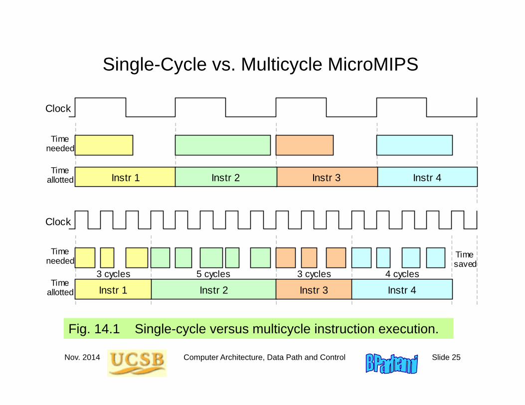
Single-Cycle vs. Multicycle MicroMIPS
Fig. 14.1 Single-cycle versus multicycle instruction execution.
Clock
Clock
Instr 2 Instr 1 Instr 3 Instr 4 3 cycles 3 cycles 4 cycles 5 cycles
Time saved
Instr 1 Instr 4 Instr 3 Instr 2
Time needed
Time needed
Time allotted
Time allotted
Nov. 2014 Computer Architecture, Data Path and Control Slide 26
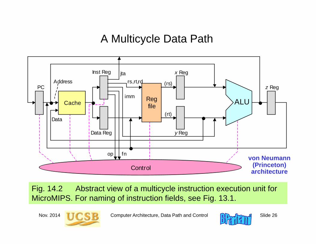
A Multicycle Data Path
Fig. 14.2 Abstract view of a multicycle instruction execution unit for MicroMIPS. For naming of instruction fields, see Fig. 13.1.
ALU
Cache
Control
Reg file
op
jta
fn
imm
rs,rt,rd (rs)
(rt)
Address
Data
Inst Reg
Data Reg
x Reg
y Reg
z Reg PC
von Neumann (Princeton)architecture

Nov. 2014 Computer Architecture, Data Path and Control Slide 27
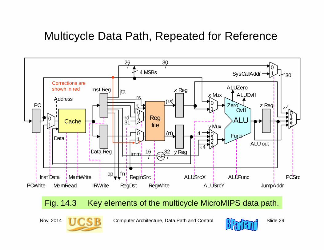
Multicycle Data Path with Control Signals Shown
Fig. 14.3 Key elements of the multicycle MicroMIPS data path.
Three major changes relative to the single-cycle data path:
1. Instruction & data caches combined
2. ALU performs double duty for address calculation
3. Registers added for intercycle data
/
16
rs
0 1
0 1 2
ALU
Cache Reg file
op
jta
fn
(rs)
(rt)
Address
Data
Inst Reg
Data Reg
x Reg
y Reg
z Reg PC
4
ALUSrcX
ALUFunc
MemWrite MemRead
RegInSrc
4
rd
RegDst RegWrite
/
32
Func
ALUOvfl
Ovfl
31
PCSrc PCWrite IRWrite
ALU out
0 1
0 1
0 1 2 3
0 1 2 3
InstData ALUSrcY
SysCallAddr
/
26
4
rt
ALUZero
Zero
x Mux
y Mux
0 1
JumpAddr
4 MSBs
/
30
30
SE
imm
2
Corrections are shown in red
Nov. 2014 Computer Architecture, Data Path and Control Slide 28
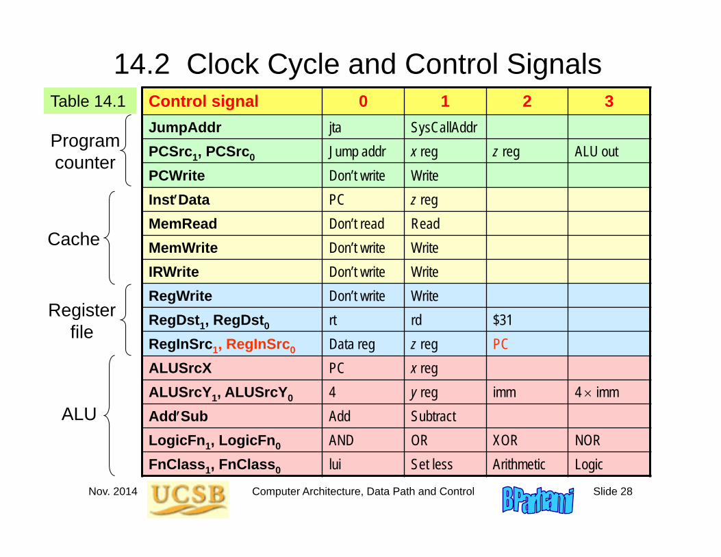
14.2 Clock Cycle and Control SignalsTable 14.1 Control signal 0 1 2 3
JumpAddr jta SysCallAddrPCSrc1, PCSrc0 Jump addr x reg z reg ALU outPCWrite Don’t write WriteInstData PC z regMemRead Don’t read ReadMemWrite Don’t write WriteIRWrite Don’t write WriteRegWrite Don’t write WriteRegDst1, RegDst0 rt rd $31RegInSrc1, RegInSrc0 Data reg z reg PCALUSrcX PC x regALUSrcY1, ALUSrcY0 4 y reg imm 4 immAddSub Add SubtractLogicFn1, LogicFn0 AND OR XOR NORFnClass1, FnClass0 lui Set less Arithmetic Logic
Register file
ALU
Cache
Program counter
Nov. 2014 Computer Architecture, Data Path and Control Slide 29
Multicycle Data Path, Repeated for Reference
Fig. 14.3 Key elements of the multicycle MicroMIPS data path.
/
16
rs
0 1
0 1 2
ALU
Cache Reg file
op
jta
fn
(rs)
(rt)
Address
Data
Inst Reg
Data Reg
x Reg
y Reg
z Reg PC
4
ALUSrcX
ALUFunc
MemWrite MemRead
RegInSrc
4
rd
RegDst RegWrite
/
32
Func
ALUOvfl
Ovfl
31
PCSrc PCWrite IRWrite
ALU out
0 1
0 1
0 1 2 3
0 1 2 3
InstData ALUSrcY
SysCallAddr
/
26
4
rt
ALUZero
Zero
x Mux
y Mux
0 1
JumpAddr
4 MSBs
/
30
30
SE
imm
2
Corrections are shown in red
Nov. 2014 Computer Architecture, Data Path and Control Slide 30
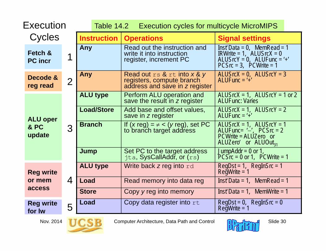
Execution Cycles
Table 14.2 Execution cycles for multicycle MicroMIPS
Instruction Operations Signal settingsAny Read out the instruction and
write it into instruction register, increment PC
InstData = 0, MemRead = 1IRWrite = 1, ALUSrcX = 0ALUSrcY = 0, ALUFunc = ‘+’PCSrc = 3, PCWrite = 1
Any Read out rs & rt into x & yregisters, compute branch address and save in z register
ALUSrcX = 0, ALUSrcY = 3ALUFunc = ‘+’
ALU type Perform ALU operation and save the result in z register
ALUSrcX = 1, ALUSrcY = 1 or 2ALUFunc: Varies
Load/Store Add base and offset values, save in z register
ALUSrcX = 1, ALUSrcY = 2ALUFunc = ‘+’
Branch If (x reg) = < (y reg), set PC to branch target address
ALUSrcX = 1, ALUSrcY = 1ALUFunc= ‘’, PCSrc = 2PCWrite = ALUZero or ALUZero or ALUOut31
Jump Set PC to the target address jta, SysCallAddr, or (rs)
JumpAddr = 0 or 1,PCSrc = 0 or 1, PCWrite = 1
ALU type Write back z reg into rd RegDst = 1, RegInSrc = 1RegWrite = 1
Load Read memory into data reg InstData = 1, MemRead = 1Store Copy y reg into memory InstData = 1, MemWrite = 1Load Copy data register into rt RegDst = 0, RegInSrc = 0
RegWrite = 1
Fetch & PC incr
Decode & reg read
ALU oper & PC update
Reg write or mem access
Reg write for lw
1
2
3
4
5
Nov. 2014 Computer Architecture, Data Path and Control Slide 31
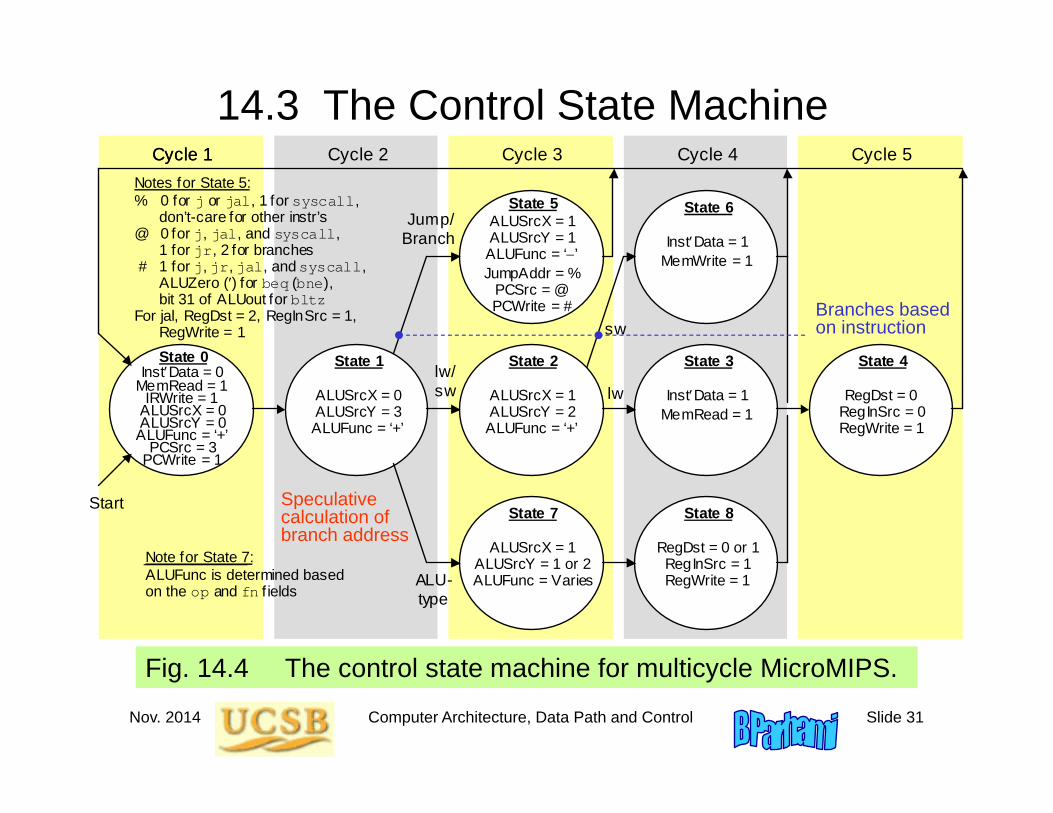
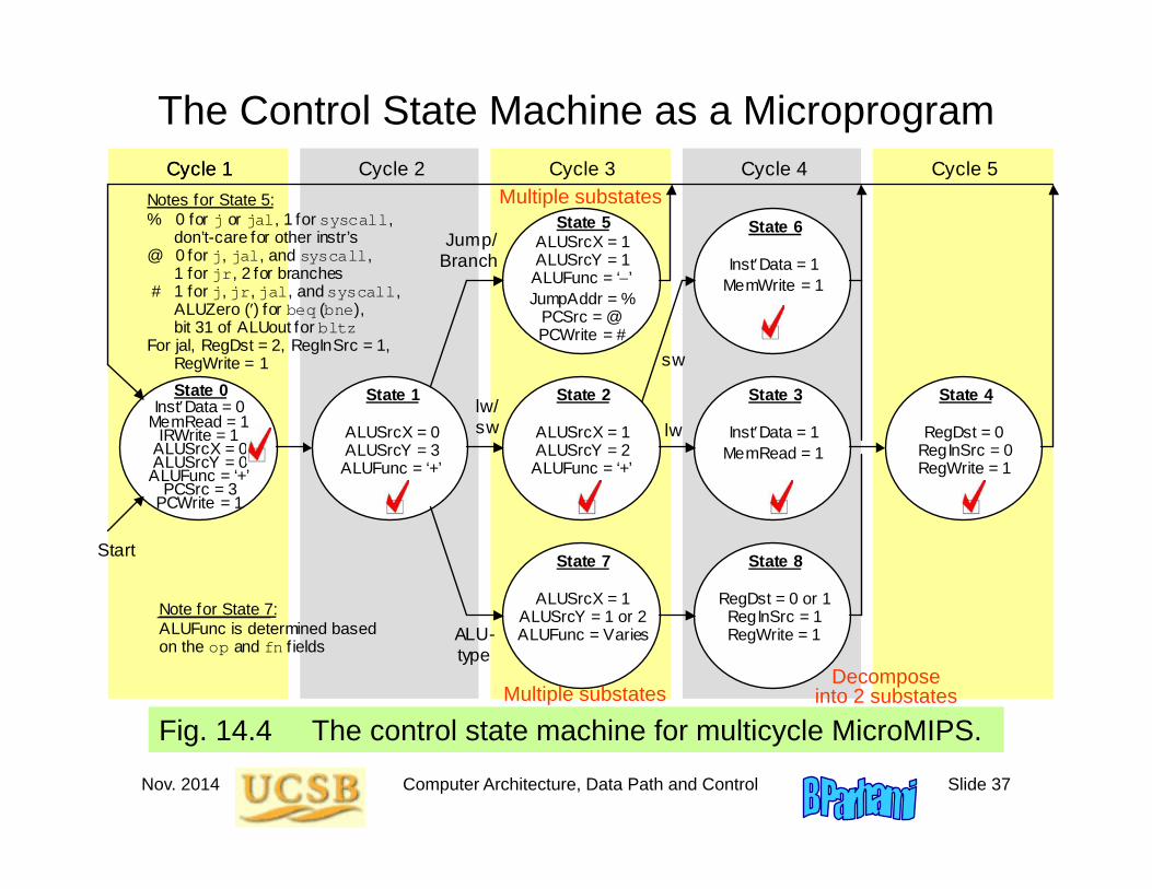
14.3 The Control State Machine
Fig. 14.4 The control state machine for multicycle MicroMIPS.
State 0
InstData = 0 MemRead = 1
IRWrite = 1 ALUSrcX = 0 ALUSrcY = 0 ALUFunc = ‘+’
PCSrc = 3 PCWrite = 1
Start
Cycle 1 Cycle 3 Cycle 2 Cycle 1 Cycle 4 Cycle 5
ALU- type
lw/ sw lw
sw
State 1
ALUSrcX = 0 ALUSrcY = 3 ALUFunc = ‘+’
State 5 ALUSrcX = 1 ALUSrcY = 1 ALUFunc = ‘’ JumpAddr = %
PCSrc = @ PCWrite = #
State 8
RegDst = 0 or 1 RegInSrc = 1 RegWrite = 1
State 7
ALUSrcX = 1 ALUSrcY = 1 or 2 ALUFunc = Varies
State 6
InstData = 1 MemWrite = 1
State 4
RegDst = 0 RegInSrc = 0 RegWrite = 1
State 2
ALUSrcX = 1 ALUSrcY = 2 ALUFunc = ‘+’
State 3
InstData = 1 MemRead = 1
Jump/ Branch
Notes for State 5: % 0 for j or jal, 1 for syscall, don’t-care for other instr’s @ 0 for j, jal, and syscall, 1 for jr, 2 for branches # 1 for j, jr, jal, and syscall, ALUZero () for beq (bne), bit 31 of ALUout for bltz For jal, RegDst = 2, RegInSrc = 1, RegWrite = 1
Note for State 7: ALUFunc is determined based on the op and fn f ields
Speculative calculation of branch address
Branches based on instruction
Nov. 2014 Computer Architecture, Data Path and Control Slide 32
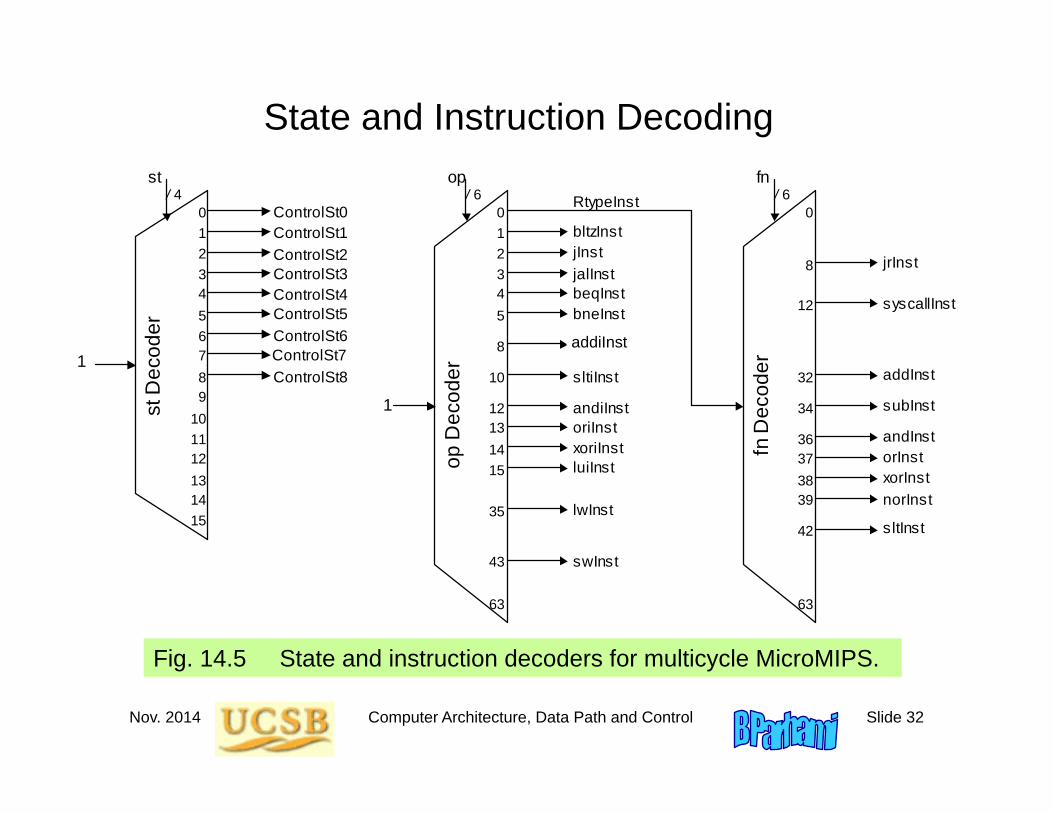
State and Instruction Decoding
Fig. 14.5 State and instruction decoders for multicycle MicroMIPS.
jrInst
norInst
sltInst
orInst xorInst
syscallInst
andInst
addInst
subInst
RtypeInst
bltzInst jInst jalInst beqInst bneInst
sltiInst
andiInst oriInst xoriInst luiInst
lwInst
swInst
andiInst
1
0 1 2 3 4 5
10
12 13 14 15
35
43
63
8
op D
ecod
er
fn D
ecod
er
/ 6 / 6 op fn
0
8
12
32
34
36 37 38 39
42
63
ControlSt0 ControlSt1 ControlSt2 ControlSt3 ControlSt4 ControlSt5
ControlSt8
ControlSt6 1
st D
ecod
er
/ 4
st
0 1 2 3 4 5
7
12 13 14 15
8 9 10
6
11
ControlSt7
addiInst
Nov. 2014 Computer Architecture, Data Path and Control Slide 33
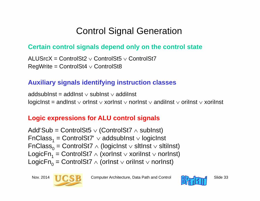
Control Signal GenerationCertain control signals depend only on the control state
ALUSrcX = ControlSt2 ControlSt5 ControlSt7RegWrite = ControlSt4 ControlSt8
Auxiliary signals identifying instruction classes
addsubInst = addInst subInst addiInstlogicInst = andInst orInst xorInst norInst andiInst oriInst xoriInst
Logic expressions for ALU control signals
AddSub = ControlSt5 (ControlSt7 subInst)FnClass1 = ControlSt7 addsubInst logicInstFnClass0 = ControlSt7 (logicInst sltInst sltiInst)LogicFn1 = ControlSt7 (xorInst xoriInst norInst)LogicFn0 = ControlSt7 (orInst oriInst norInst)
Nov. 2014 Computer Architecture, Data Path and Control Slide 34
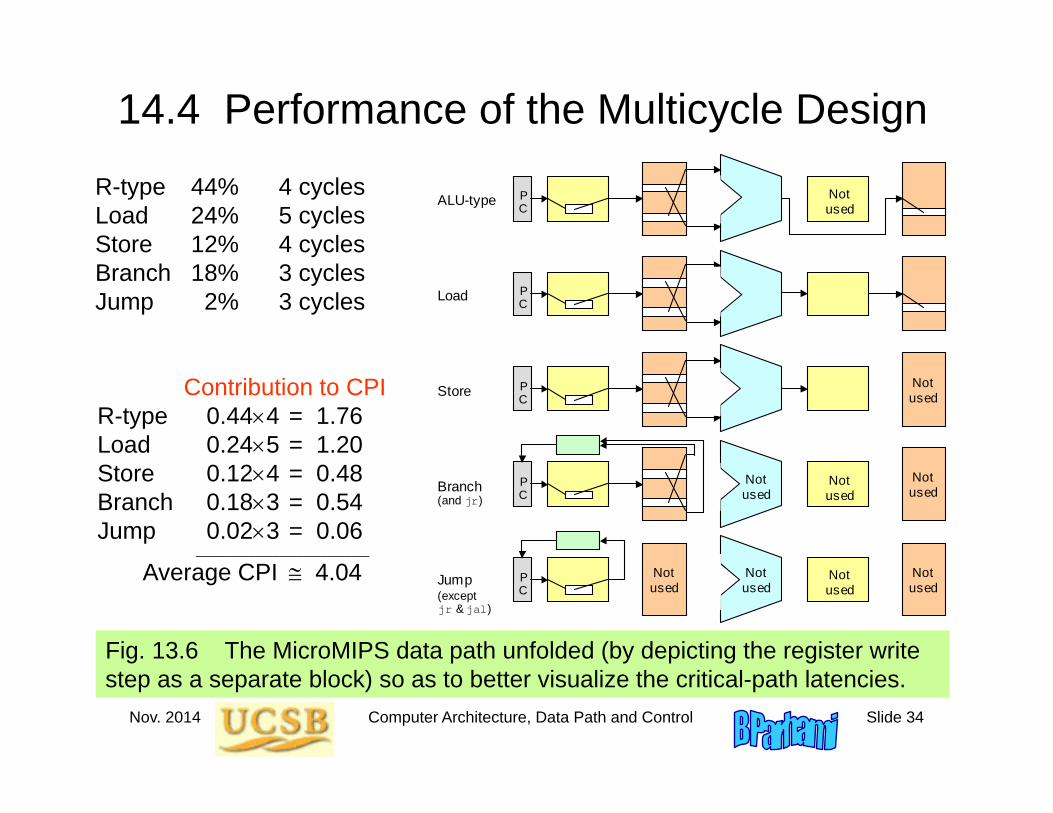
14.4 Performance of the Multicycle Design
Fig. 13.6 The MicroMIPS data path unfolded (by depicting the register write step as a separate block) so as to better visualize the critical-path latencies.
P C
P C
P C
P C
P C
ALU-type
Load
Store
Branch
Jump
Not used
Not used
Not used
Not used
Not used
Not used
Not used
Not used
Not used
(and jr)
(except jr & jal)
R-type 44% 4 cyclesLoad 24% 5 cyclesStore 12% 4 cyclesBranch 18% 3 cyclesJump 2% 3 cycles
Contribution to CPIR-type 0.444 = 1.76Load 0.245 = 1.20Store 0.124 = 0.48Branch 0.183 = 0.54Jump 0.023 = 0.06
_____________________________
Average CPI 4.04

Nov. 2014 Computer Architecture, Data Path and Control Slide 35
How Good is Our Multicycle Design?Clock rate of 500 MHz better than 125 MHz of single-cycle design, but still unimpressive
How does the performance compare with current processors on the market?
Not bad, where latency is concerned
A 2.5 GHz processor with 20 or so pipeline stages has a latency of about 0.420 =8ns
Throughput, however, is much better for the pipelined processor:
Up to 20 times better with single issue
Perhaps up to 100 with multiple issue
R-type 44% 4 cyclesLoad 24% 5 cyclesStore 12% 4 cyclesBranch 18% 3 cyclesJump 2% 3 cycles
Contribution to CPIR-type 0.444 = 1.76
Load 0.245 = 1.20Store 0.124 = 0.48Branch 0.183 = 0.54Jump 0.023 = 0.06
_____________________________
Average CPI 4.04
Cycle time = 2 nsClock rate = 500 MHz

Nov. 2014 Computer Architecture, Data Path and Control Slide 36
14.5 Microprogramming
State 0
InstData = 0 MemRead = 1
IRWrite = 1 ALUSrcX = 0 ALUSrcY = 0 ALUFunc = ‘+’
PCSrc = 3 PCWrite = 1
Start
Cycle 1 Cycle 3 Cycle 2 Cycle 1 Cycle 4 Cycle 5
ALU- type
lw/ sw lw
sw
State 1
ALUSrcX = 0 ALUSrcY = 3
ALUFunc = ‘+’
State 5 ALUSrcX = 1 ALUSrcY = 1 ALUFunc = ‘’ JumpAddr = %
PCSrc = @ PCWrite = #
State 8
RegDst = 0 or 1 RegInSrc = 1 RegWrite = 1
State 7
ALUSrcX = 1 ALUSrcY = 1 or 2 ALUFunc = Varies
State 6
InstData = 1 MemWrite = 1
State 4
RegDst = 0 RegInSrc = 0 RegWrite = 1
State 2
ALUSrcX = 1 ALUSrcY = 2 ALUFunc = ‘+’
State 3
InstData = 1 MemRead = 1
Jump/ Branch
Notes for State 5: % 0 for j or jal, 1 for syscall, don’t-care for other instr’s @ 0 for j, jal, and syscall, 1 for jr, 2 for branches # 1 for j, jr, jal, and syscall, ALUZero () for beq (bne), bit 31 of ALUout for bltz For jal, RegDst = 2, RegInSrc = 1, RegWrite = 1
Note for State 7: ALUFunc is determined based on the op and fn f ields
The control state machine resembles a program (microprogram)
Microinstruction
Fig. 14.6 Possible 22-bit microinstruction format for MicroMIPS.
PC control
Cache control
Register control
ALU inputs
JumpAddr PCSrc
PCWrite
InstData MemRead
MemWrite IRWrite
FnType LogicFn
AddSub ALUSrcY
ALUSrcX RegInSrc
RegDst RegWrite
Sequence control
ALU function
2bits
23
Nov. 2014 Computer Architecture, Data Path and Control Slide 37
The Control State Machine as a Microprogram
Fig. 14.4 The control state machine for multicycle MicroMIPS.
State 0
InstData = 0 MemRead = 1
IRWrite = 1 ALUSrcX = 0 ALUSrcY = 0 ALUFunc = ‘+’
PCSrc = 3 PCWrite = 1
Start
Cycle 1 Cycle 3 Cycle 2 Cycle 1 Cycle 4 Cycle 5
ALU- type
lw/ sw lw
sw
State 1
ALUSrcX = 0 ALUSrcY = 3 ALUFunc = ‘+’
State 5 ALUSrcX = 1 ALUSrcY = 1 ALUFunc = ‘’ JumpAddr = %
PCSrc = @ PCWrite = #
State 8
RegDst = 0 or 1 RegInSrc = 1 RegWrite = 1
State 7
ALUSrcX = 1 ALUSrcY = 1 or 2 ALUFunc = Varies
State 6
InstData = 1 MemWrite = 1
State 4
RegDst = 0 RegInSrc = 0 RegWrite = 1
State 2
ALUSrcX = 1 ALUSrcY = 2 ALUFunc = ‘+’
State 3
InstData = 1 MemRead = 1
Jump/ Branch
Notes for State 5: % 0 for j or jal, 1 for syscall, don’t-care for other instr’s @ 0 for j, jal, and syscall, 1 for jr, 2 for branches # 1 for j, jr, jal, and syscall, ALUZero () for beq (bne), bit 31 of ALUout for bltz For jal, RegDst = 2, RegInSrc = 1, RegWrite = 1
Note for State 7: ALUFunc is determined based on the op and fn f ields
Decompose into 2 substatesMultiple substates
Multiple substates
Nov. 2014 Computer Architecture, Data Path and Control Slide 38
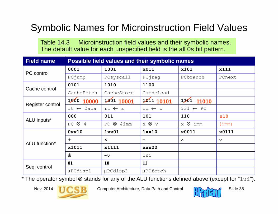
Symbolic Names for Microinstruction Field ValuesTable 14.3 Microinstruction field values and their symbolic names. The default value for each unspecified field is the all 0s bit pattern.
Field name Possible field values and their symbolic names
PC control0001 1001 x011 x101 x111
PCjump PCsyscall PCjreg PCbranch PCnext
Cache control0101 1010 1100
CacheFetch CacheStore CacheLoad
Register control1000 1001 1011 1101
rt Data rt z rd z $31 PC
ALU inputs*000 011 101 110
PC 4 PC 4imm x y x imm
ALU function*
0xx10 1xx01 1xx10 x0011 x0111
+ <
x1011 x1111 xxx00
lui
Seq. control01 10 11PCdisp1 PCdisp2 PCfetch
* The operator symbol stands for any of the ALU functions defined above (except for “lui”).
10000 10001 10101 11010
x10
(imm)
Nov. 2014 Computer Architecture, Data Path and Control Slide 39
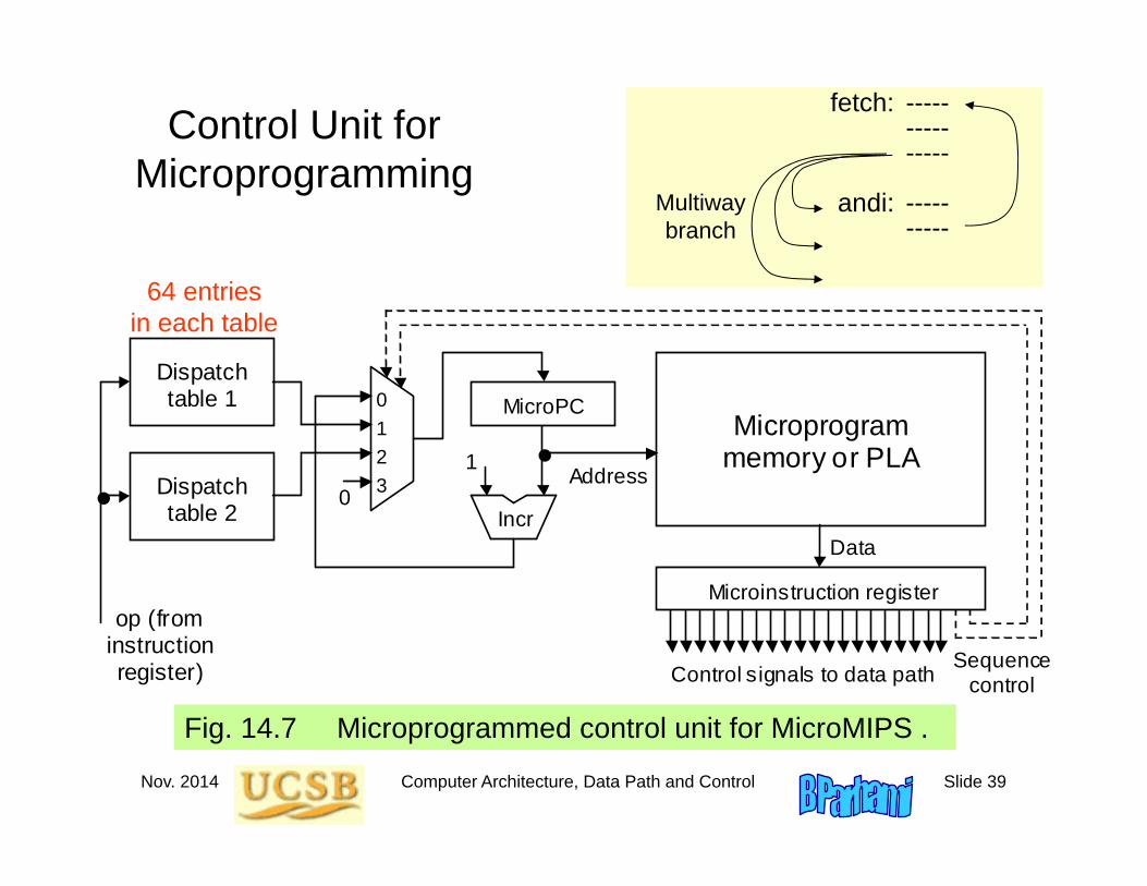
Control Unit for Microprogramming
Fig. 14.7 Microprogrammed control unit for MicroMIPS .
Microprogram memory or PLA
op (from instruction register) Control signals to data path
Address 1
Incr
MicroPC
Data
0
Sequence control
0 1 2 3
Dispatch table 1
Dispatch table 2
Microinstruction register
fetch: ---------------
andi: ----------
Multiway branch
64 entries in each table

Nov. 2014 Computer Architecture, Data Path and Control Slide 40
Microprogram for MicroMIPS
Fig. 14.8 The complete MicroMIPS microprogram.
fetch: PCnext, CacheFetch # State 0 (start)PC + 4imm, PCdisp1 # State 1
lui1: lui(imm) # State 7luirt z, PCfetch # State 8lui
add1: x + y # State 7addrd z, PCfetch # State 8add
sub1: x - y # State 7subrd z, PCfetch # State 8sub
slt1: x - y # State 7sltrd z, PCfetch # State 8slt
addi1: x + imm # State 7addirt z, PCfetch # State 8addi
slti1: x - imm # State 7sltirt z, PCfetch # State 8slti
and1: x y # State 7andrd z, PCfetch # State 8and
or1: x y # State 7orrd z, PCfetch # State 8or
xor1: x y # State 7xorrd z, PCfetch # State 8xor
nor1: x y # State 7norrd z, PCfetch # State 8nor
andi1: x imm # State 7andirt z, PCfetch # State 8andi
ori1: x imm # State 7orirt z, PCfetch # State 8ori
xori: x imm # State 7xorirt z, PCfetch # State 8xori
lwsw1: x + imm, mPCdisp2 # State 2lw2: CacheLoad # State 3
rt Data, PCfetch # State 4sw2: CacheStore, PCfetch # State 6j1: PCjump, PCfetch # State 5jjr1: PCjreg, PCfetch # State 5jrbranch1: PCbranch, PCfetch # State 5branchjal1: PCjump, $31PC, PCfetch # State 5jalsyscall1:PCsyscall, PCfetch # State 5syscall
37 microinstructions
Nov. 2014 Computer Architecture, Data Path and Control Slide 41
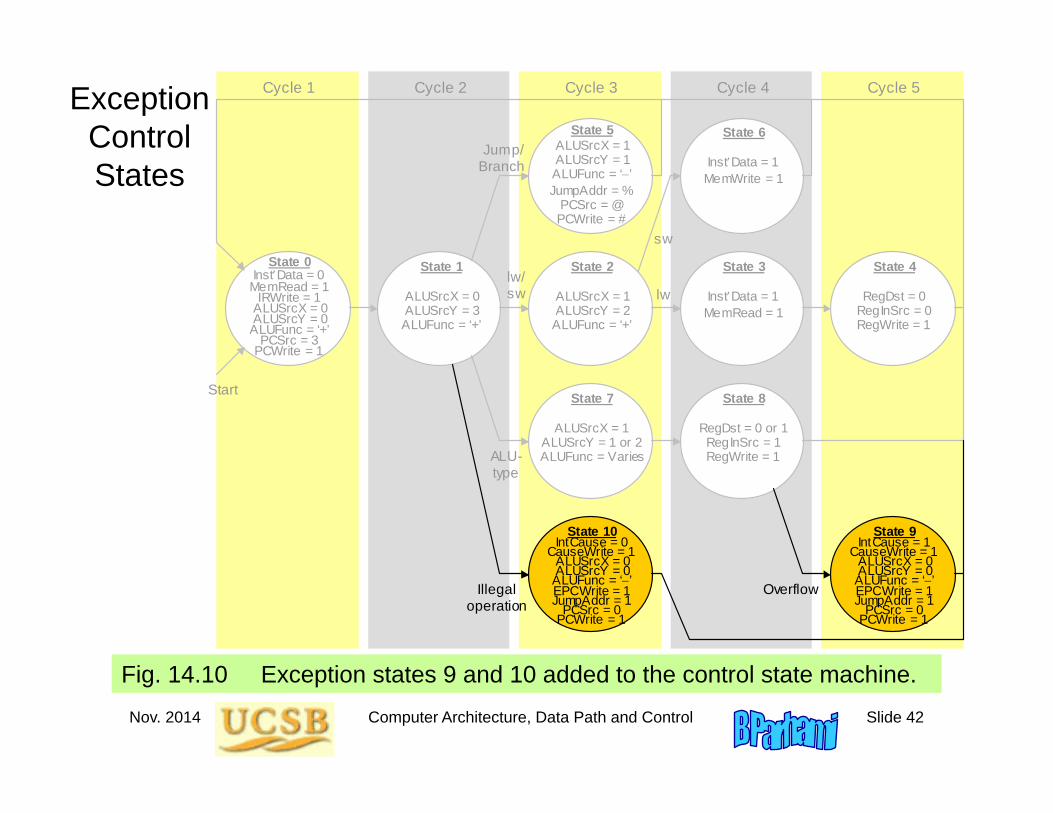
14.6 Exception HandlingExceptions and interrupts alter the normal program flow
Examples of exceptions (things that can go wrong):
ALU operation leads to overflow (incorrect result is obtained) Opcode field holds a pattern not representing a legal operation Cache error-code checker deems an accessed word invalid Sensor signals a hazardous condition (e.g., overheating)
Exception handler is an OS program that takes care of the problem
Derives correct result of overflowing computation, if possible Invalid operation may be a software-implemented instruction
Interrupts are similar, but usually have external causes (e.g., I/O)
Nov. 2014 Computer Architecture, Data Path and Control Slide 42
Exception Control States
Fig. 14.10 Exception states 9 and 10 added to the control state machine.
State 0 InstData = 0 MemRead = 1
IRWrite = 1 ALUSrcX = 0 ALUSrcY = 0 ALUFunc = ‘+’
PCSrc = 3 PCWrite = 1
Start
Cycle 1 Cycle 3 Cycle 2 Cycle 4 Cycle 5
ALU- type
lw/ sw lw
sw
State 1
ALUSrcX = 0 ALUSrcY = 3 ALUFunc = ‘+’
State 5 ALUSrcX = 1 ALUSrcY = 1 ALUFunc = ‘’ JumpAddr = %
PCSrc = @ PCWrite = #
State 8
RegDst = 0 or 1 RegInSrc = 1 RegWrite = 1
State 7
ALUSrcX = 1 ALUSrcY = 1 or 2 ALUFunc = Varies
State 6
InstData = 1 MemWrite = 1
State 4
RegDst = 0 RegInSrc = 0 RegWrite = 1
State 2
ALUSrcX = 1 ALUSrcY = 2 ALUFunc = ‘+’
State 3
InstData = 1 MemRead = 1
Jump/ Branch
State 10 IntCause = 0
CauseWrite = 1 ALUSrcX = 0 ALUSrcY = 0 ALUFunc = ‘’ EPCWrite = 1 JumpAddr = 1
PCSrc = 0 PCWrite = 1
State 9 IntCause = 1
CauseWrite = 1 ALUSrcX = 0 ALUSrcY = 0 ALUFunc = ‘’ EPCWrite = 1 JumpAddr = 1
PCSrc = 0 PCWrite = 1
Illegal operation
Overflow
Nov. 2014 Computer Architecture, Data Path and Control Slide 43
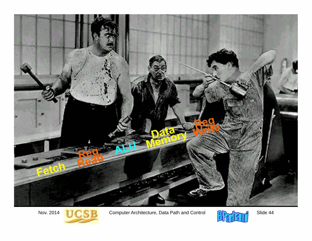
15 Pipelined Data PathsPipelining is now used in even the simplest of processors
• Same principles as assembly lines in manufacturing• Unlike in assembly lines, instructions not independent
Topics in This Chapter15.1 Pipelining Concepts
15.2 Pipeline Stalls or Bubbles
15.3 Pipeline Timing and Performance
15.4 Pipelined Data Path Design
15.5 Pipelined Control
15.6 Optimal Pipelining
Nov. 2014 Computer Architecture, Data Path and Control Slide 44
Nov. 2014 Computer Architecture, Data Path and Control Slide 45
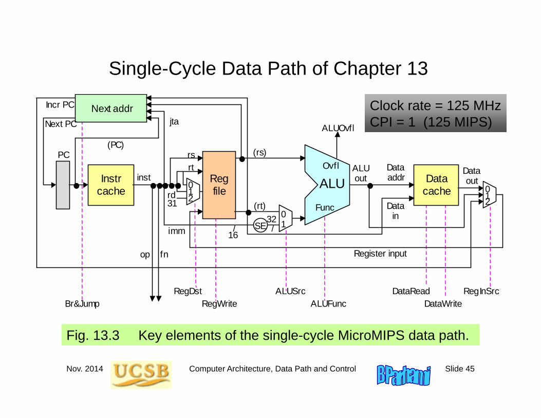
Single-Cycle Data Path of Chapter 13
Fig. 13.3 Key elements of the single-cycle MicroMIPS data path.
/
ALU
Data cache
Instr cache
Next addr
Reg file
op
jta
fn
inst
imm
rs (rs)
(rt)
Data addr
Data in 0
1
ALUSrc ALUFunc DataWrite
DataRead
SE
RegInSrc
rt
rd
RegDst RegWrite
32 / 16
Register input
Data out
Func
ALUOvfl
Ovfl
31
0 1 2
Next PC
Incr PC
(PC)
Br&Jump
ALU out
PC
0 1 2
Clock rate = 125 MHzCPI = 1 (125 MIPS)
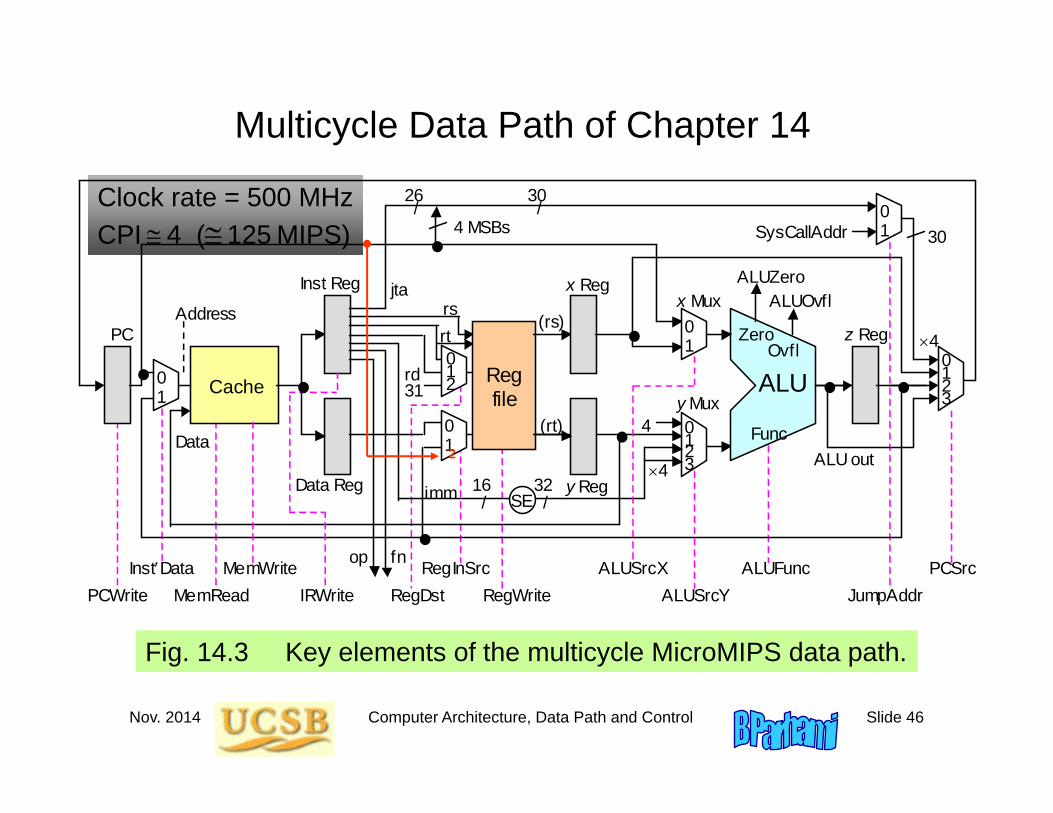
Nov. 2014 Computer Architecture, Data Path and Control Slide 46
Multicycle Data Path of Chapter 14
Fig. 14.3 Key elements of the multicycle MicroMIPS data path.
Clock rate = 500 MHzCPI 4 (125 MIPS)
/
16
rs
0 1
0 1 2
ALU
Cache Reg file
op
jta
fn
(rs)
(rt)
Address
Data
Inst Reg
Data Reg
x Reg
y Reg
z Reg PC
4
ALUSrcX
ALUFunc
MemWrite MemRead
RegInSrc
4
rd
RegDst RegWrite
/
32
Func
ALUOvfl
Ovfl
31
PCSrc PCWrite IRWrite
ALU out
0 1
0 1
0 1 2 3
0 1 2 3
InstData ALUSrcY
SysCallAddr
/
26
4
rt
ALUZero
Zero
x Mux
y Mux
0 1
JumpAddr
4 MSBs
/
30
30
SE
imm
2

Nov. 2014 Computer Architecture, Data Path and Control Slide 47
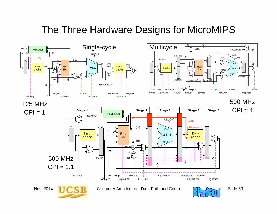
Getting the Best of Both Worlds
Single-cycle:Clock rate = 125 MHz
CPI = 1
Multicycle:Clock rate = 500 MHz
CPI 4
Pipelined:Clock rate = 500 MHz
CPI 1
Single-cycle analogy:Doctor appointments scheduled for 60 min per patient
Multicycle analogy:Doctor appointments scheduled in 15-min increments

Nov. 2014 Computer Architecture, Data Path and Control Slide 48
15.1 Pipelining Concepts
Fig. 15.1 Pipelining in the student registration process.
Strategies for improving performance1 – Use multiple independent data paths accepting several instructions
that are read out at once: multiple-instruction-issue or superscalar
2 – Overlap execution of several instructions, starting the next instruction before the previous one has run to completion: (super)pipelined
Approval Cashier Registrar ID photo Pickup
Start here
Exit
1 2 3 4 5 2
Nov. 2014 Computer Architecture, Data Path and Control Slide 49
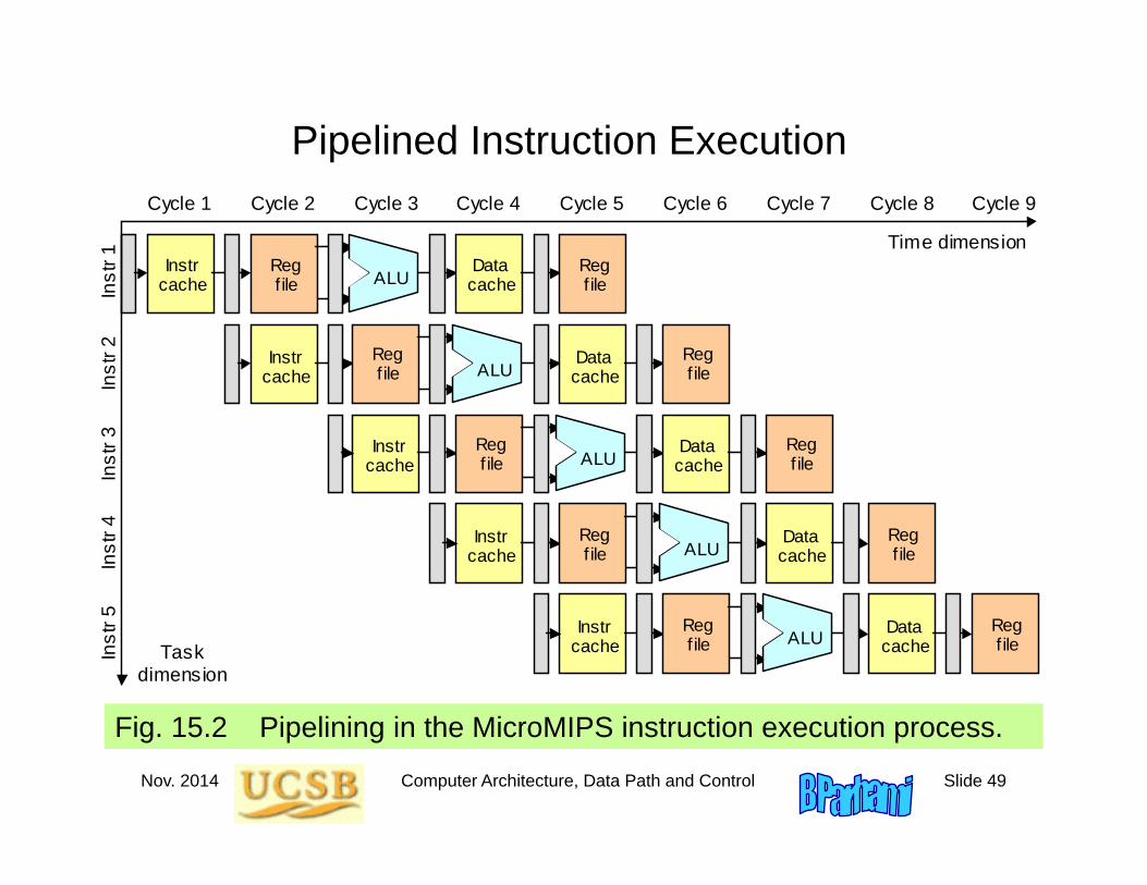
Pipelined Instruction Execution
Fig. 15.2 Pipelining in the MicroMIPS instruction execution process.
Cycle 7 Cycle 6 Cycle 5 Cycle 4 Cycle 3 Cycle 2 Cycle 1 Cycle 8
Reg file
Reg f ile ALU
Reg file
Reg f ile ALU
Reg file
Reg f ile ALU
Reg f ile
Reg f ile ALU
Reg file
Reg f ile ALU
Cycle 9
Instr cache
Instr cache
Instr cache
Instr cache
Instr cache
Data cache
Data cache
Data cache
Data cache
Data cache
Time dimension
Task dimension
Ins
tr 1
Ins
tr 2
Ins
tr 3
Ins
tr 4
Ins
tr 5
Nov. 2014 Computer Architecture, Data Path and Control Slide 50
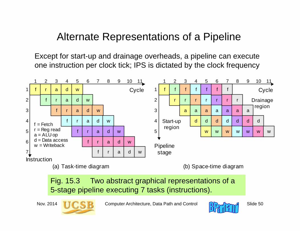
Alternate Representations of a Pipeline
Fig. 15.3 Two abstract graphical representations of a 5-stage pipeline executing 7 tasks (instructions).
1
2
3
4
5
1
2
3
4
5
6
7
(a) Task-time diagram (b) Space-time diagram
Cycle
Instruction
Cycle
Pipeline stage
1 2 3 4 5 6 7 8 9 10 11 1 2 3 4 5 6 7 8 9 10 11
Start-up region
Drainageregion
a
a
a
a
a
a
a
w
w
w
w
w
w
w
f
f
f
f
f
f
f
r
r
r
r
r
r
r
d
d
d
d
d
d
d
a a a a a a a
w w w w w w w
d d d d d d d
r r r r r r r
f f f f f f f
f = Fetch r = Reg read a = ALU op d = Data access w = Writeback
Except for start-up and drainage overheads, a pipeline can execute one instruction per clock tick; IPS is dictated by the clock frequency
Nov. 2014 Computer Architecture, Data Path and Control Slide 51
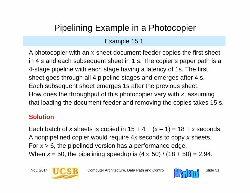
Pipelining Example in a PhotocopierExample 15.1
A photocopier with an x-sheet document feeder copies the first sheet in 4 s and each subsequent sheet in 1 s. The copier’s paper path is a 4-stage pipeline with each stage having a latency of 1s. The first sheet goes through all 4 pipeline stages and emerges after 4 s. Each subsequent sheet emerges 1s after the previous sheet. How does the throughput of this photocopier vary with x, assuming that loading the document feeder and removing the copies takes 15 s.
Solution
Each batch of x sheets is copied in 15 + 4 + (x – 1) = 18 + x seconds. A nonpipelined copier would require 4x seconds to copy x sheets. For x > 6, the pipelined version has a performance edge. When x = 50, the pipelining speedup is (4 50) / (18 + 50) = 2.94.
Nov. 2014 Computer Architecture, Data Path and Control Slide 52
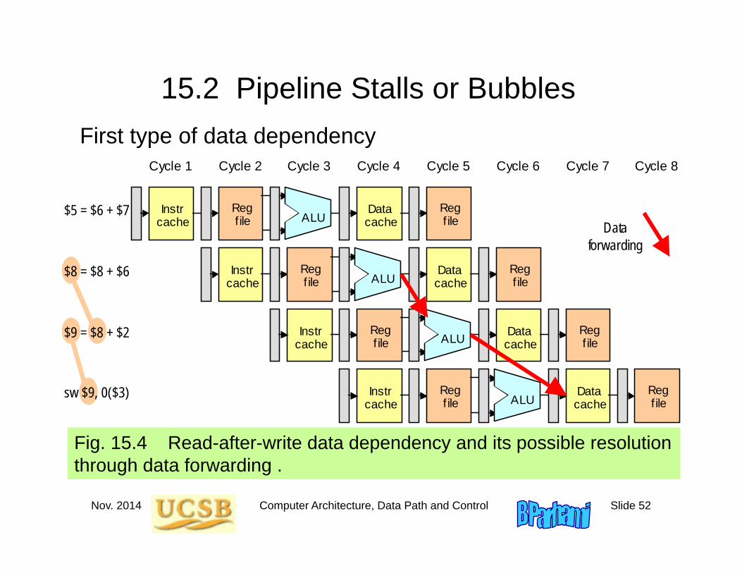
15.2 Pipeline Stalls or Bubbles
Fig. 15.4 Read-after-write data dependency and its possible resolution through data forwarding .
Cycle 7 Cycle 6 Cycle 5 Cycle 4 Cycle 3 Cycle 2 Cycle 1 Cycle 8
Reg f ile
Reg f ile ALU
Reg file
Reg file ALU
Reg f ile
Reg file ALU
Reg f ile
Reg f ile ALU
$5 = $6 + $7
$8 = $8 + $6
$9 = $8 + $2
sw $9, 0($3)
Data forwarding
Instr cache
Instr cache
Instr cache
Instr cache
Data cache
Data cache
Data cache
Data cache
First type of data dependency
Nov. 2014 Computer Architecture, Data Path and Control Slide 53
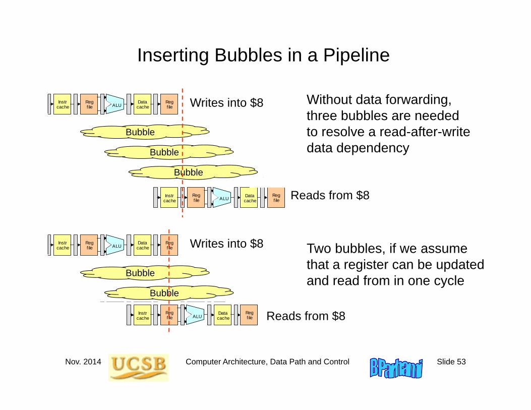
Inserting Bubbles in a Pipeline
Without data forwarding, three bubbles are needed to resolve a read-after-write data dependency
Cycle 7 Cycle 6 Cycle 5 Cycle 4 Cycle 3 Cycle 2 Cycle 1 Cycle 8
Reg f ile
Reg file ALU
Reg f ile
Reg f ile ALU
Reg file
Reg f ile ALU
Reg file
Reg f ile ALU
Reg f ile
Reg f ile ALU
Cycle 9
Instr cache
Instr cache
Instr cache
Instr cache
Instr cache
Data cache
Data cache
Data cache
Data cache
Data cache
Time dimension
Task dimension
Ins
tr 1
Ins
tr 2
Ins
tr 3
Ins
tr 4
Ins
tr 5
Bubble
Bubble
Bubble
Writes into $8
Reads from $8
Cycle 7 Cycle 6 Cycle 5 Cycle 4 Cycle 3 Cycle 2 Cycle 1 Cycle 8
Reg f ile
Reg file ALU
Reg f ile
Reg f ile ALU
Reg file
Reg f ile ALU
Reg file
Reg f ile ALU
Reg f ile
Reg f ile ALU
Cycle 9
Instr cache
Instr cache
Instr cache
Instr cache
Instr cache
Data cache
Data cache
Data cache
Data cache
Data cache
Time dimension
Task dimension
Ins
tr 1
Ins
tr 2
Ins
tr 3
Ins
tr 4
Ins
tr 5
Bubble
Bubble
Writes into $8
Reads from $8
Two bubbles, if we assume that a register can be updated and read from in one cycle

Nov. 2014 Computer Architecture, Data Path and Control Slide 54
Second Type of Data Dependency
Fig. 15.5 Read-after-load data dependency and its possible resolution through bubble insertion and data forwarding.
Cycle 7 Cycle 6 Cycle 5 Cycle 4 Cycle 3 Cycle 2 Cycle 1 Cycle 8
Data mem
Instr mem
Reg file
Reg f ile ALU
Data mem
Instr mem
Reg f ile
Reg f ile ALU
Data mem
Instr mem
Reg f ile
Reg f ile ALU
sw $6, . . .
lw $8, . . .
Insert bubble?
$9 = $8 + $2
Data mem
Instr mem
Reg file
Reg f ile ALU
Reorder?
Without data forwarding, three (two) bubbles are needed to resolve a read-after-load data dependency
Nov. 2014 Computer Architecture, Data Path and Control Slide 55
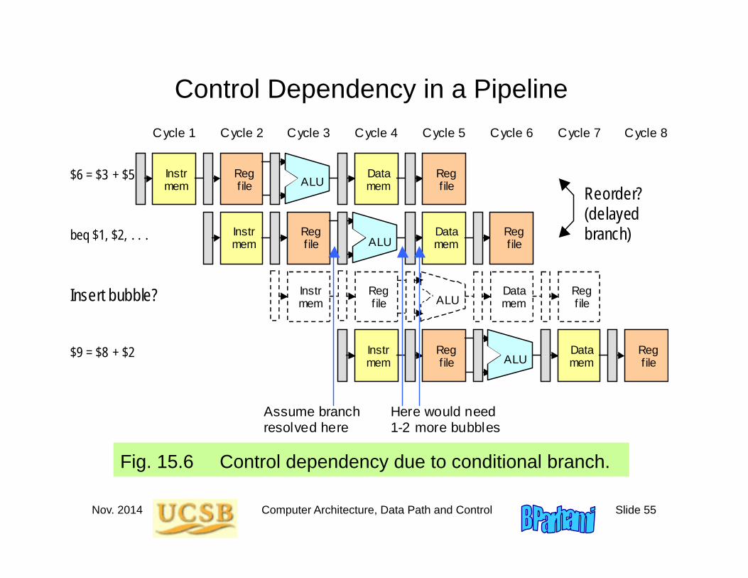
Control Dependency in a Pipeline
Fig. 15.6 Control dependency due to conditional branch.
Cycle 7 Cycle 6 Cycle 5 Cycle 4 Cycle 3 Cycle 2 Cycle 1 Cycle 8
Data mem
Instr mem
Reg f ile
Reg f ile ALU
Data mem
Instr mem
Reg file
Reg file ALU
Data mem
Instr mem
Reg f ile
Reg file ALU
$6 = $3 + $5
beq $1, $2, . . .
Insert bubble?
$9 = $8 + $2
Data mem
Instr mem
Reg f ile
Reg f ile ALU
Reorder? (delayed branch)
Assume branch resolved here
Here would need 1-2 more bubbles

Nov. 2014 Computer Architecture, Data Path and Control Slide 56
15.3 Pipeline Timing and Performance
Fig. 15.7 Pipelined form of a function unit with latching overhead.
Stage 1
Stage 2
Stage 3
Stage q 1
Stage q
t/q
Function unit
t
. . .
Latching of results
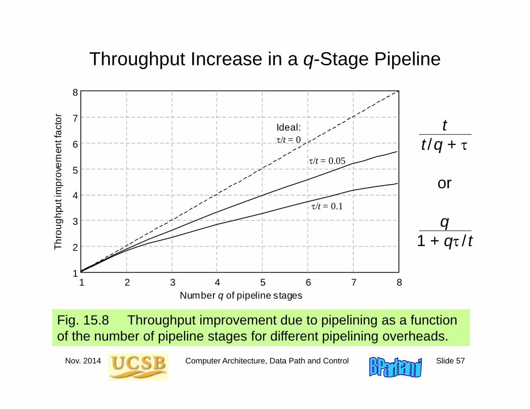
Nov. 2014 Computer Architecture, Data Path and Control Slide 57
Fig. 15.8 Throughput improvement due to pipelining as a function of the number of pipeline stages for different pipelining overheads.
Throughput Increase in a q-Stage Pipeline
1 2 3 4 5 6 7 8 Number q of pipeline stages
Thro
ughp
ut im
prov
emen
t fac
tor
1
2
3
4
5
6
7
8
Ideal: /t = 0
/t = 0.1
/t = 0.05
tt /q +
or
q1 + q / t
Nov. 2014 Computer Architecture, Data Path and Control Slide 58
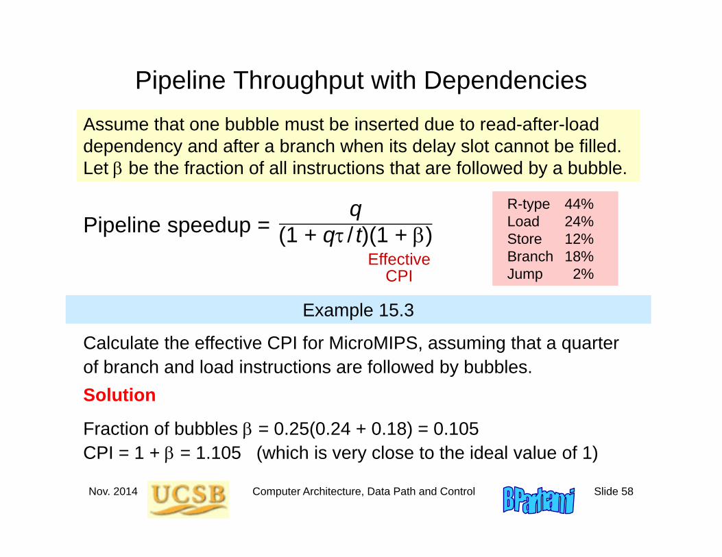
Assume that one bubble must be inserted due to read-after-load dependency and after a branch when its delay slot cannot be filled.Let be the fraction of all instructions that are followed by a bubble.
Pipeline Throughput with Dependencies
q(1 + q / t)(1 + )Pipeline speedup =
R-type 44%Load 24%Store 12%Branch 18%Jump 2%
Example 15.3
Calculate the effective CPI for MicroMIPS, assuming that a quarter of branch and load instructions are followed by bubbles.Solution
Fraction of bubbles = 0.25(0.24 + 0.18) = 0.105CPI = 1 + = 1.105 (which is very close to the ideal value of 1)
EffectiveCPI
Nov. 2014 Computer Architecture, Data Path and Control Slide 59
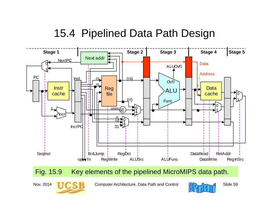
15.4 Pipelined Data Path Design
Fig. 15.9 Key elements of the pipelined MicroMIPS data path. ALU
Data
cache Instr
cache
Next addr
Reg file
op fn
inst
imm
rs (rs)
(rt)
Data addr
ALUSrc ALUFunc DataWrite DataRead
RegInSrc
rt
rd
RegDst RegWrite
Func
ALUOvfl
Ovfl
IncrPC
Br&Jump
PC
1 Incr
0 1
rt
31
0 1 2
NextPC
0 1
SeqInst
0 1 2
0 1
RetAddr
Stage 1 Stage 2 Stage 3 Stage 4 Stage 5
SE
Address
Data

Nov. 2014 Computer Architecture, Data Path and Control Slide 60
15.5 Pipelined Control
Fig. 15.10 Pipelined control signals. ALU
Data
cache Instr
cache
Next addr
Reg file
op fn
inst
imm
rs (rs)
(rt)
Data addr
ALUSrc ALUFunc
DataWrite DataRead
RegInSrc
rt
rd
RegDst RegWrite
Func
ALUOvfl
Ovfl
IncrPC
Br&Jump
PC
1 Incr
0 1
rt
31
0 1 2
NextPC
0 1
SeqInst
0 1 2
0 1
RetAddr
Stage 1 Stage 2 Stage 3 Stage 4 Stage 5
SE
5 3
2
Address
Data
Nov. 2014 Computer Architecture, Data Path and Control Slide 61
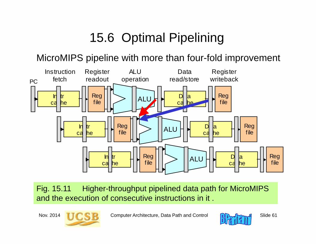
15.6 Optimal Pipelining
Fig. 15.11 Higher-throughput pipelined data path for MicroMIPS and the execution of consecutive instructions in it .
Data cache
Instr cache
Data cache
Instr cache
Data cache
Instr cache
Reg f ile
Reg file ALU
Reg file
Reg f ile ALU
Reg f ile
Reg file ALU
Instruction fetch
Register readout
ALU operation
Data read/store
Register writeback
PC
MicroMIPS pipeline with more than four-fold improvement
Nov. 2014 Computer Architecture, Data Path and Control Slide 62
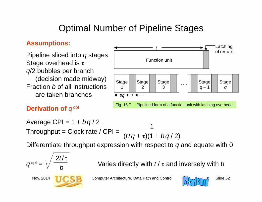
Optimal Number of Pipeline Stages
Fig. 15.7 Pipelined form of a function unit with latching overhead.
Stage 1
Stage 2
Stage 3
Stage q 1
Stage q
t/q
Function unit
t
. . .
Latching of results
Assumptions:
Pipeline sliced into q stagesStage overhead is q/2 bubbles per branch
(decision made midway)Fraction b of all instructions
are taken branches
Derivation of q opt
Average CPI = 1 + bq / 2Throughput = Clock rate / CPI =
Differentiate throughput expression with respect to q and equate with 0
q opt = Varies directly with t / and inversely with b2t /
b
1(t /q + )(1 + bq / 2)
Nov. 2014 Computer Architecture, Data Path and Control Slide 63
Pipeline register placement, Option 2
Pipelining ExampleAn example combinational-logic data path to compute z := (u + v)(w – x) / y
Add/Sub latency
2 ns
Multiply latency
6 ns
Divide latency15 ns
Throughput, original = 1/(25 10–9)= 40 M computations / s
/
+
y
u
v
w
xz
Readout, 1 ns
Write, 1 ns
Throughput, option 1 = 1/(17 10–9)= 58.8 M computations / s
Throughput, Option 2 = 1/(10 10–9)= 100 M computations / sPipeline register
placement, Option 1
Nov. 2014 Computer Architecture, Data Path and Control Slide 64
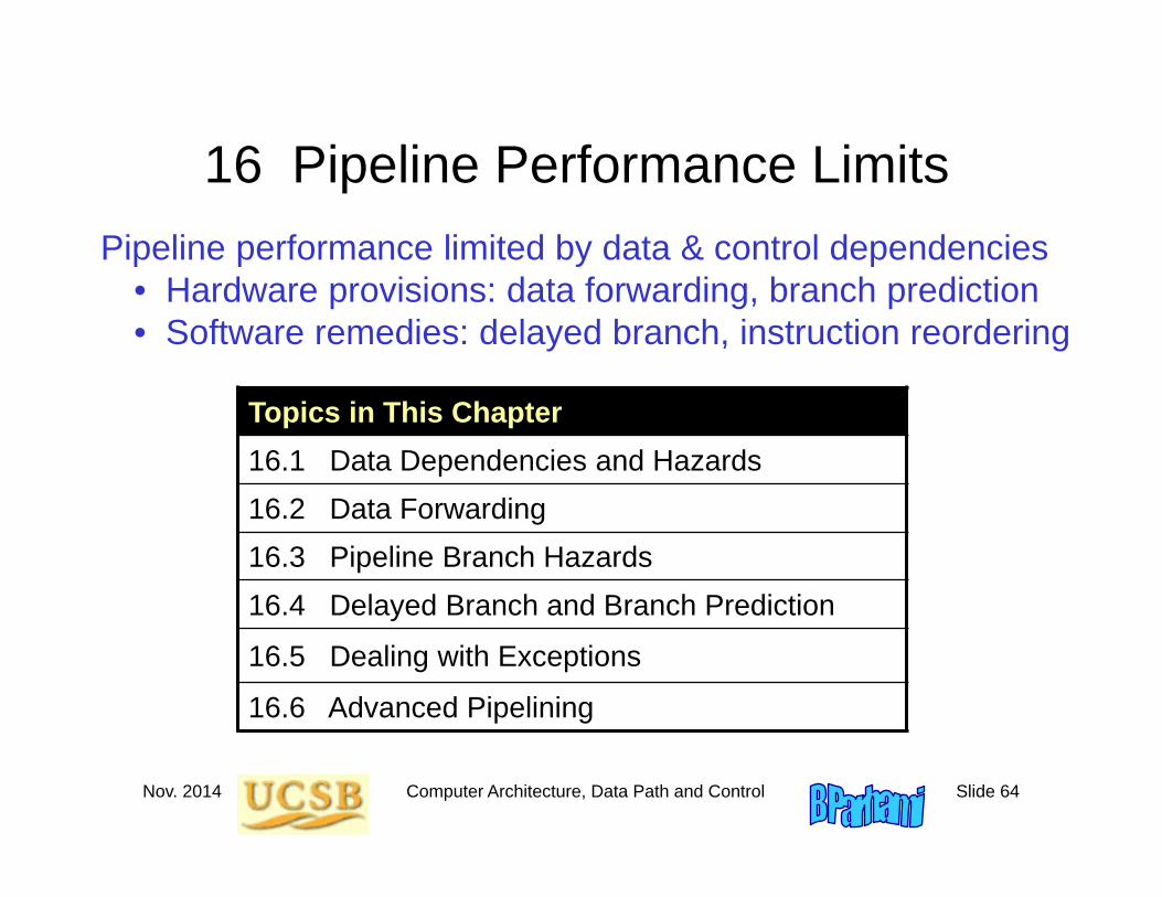
16 Pipeline Performance LimitsPipeline performance limited by data & control dependencies
• Hardware provisions: data forwarding, branch prediction• Software remedies: delayed branch, instruction reordering
Topics in This Chapter16.1 Data Dependencies and Hazards16.2 Data Forwarding16.3 Pipeline Branch Hazards16.4 Delayed Branch and Branch Prediction
16.5 Dealing with Exceptions
16.6 Advanced Pipelining

Nov. 2014 Computer Architecture, Data Path and Control Slide 65
16.1 Data Dependencies and Hazards
Fig. 16.1 Data dependency in a pipeline.
Cycle 7 Cycle 6 Cycle 5 Cycle 4 Cycle 3 Cycle 2 Cycle 1 Cycle 8
Reg file
Reg f ile ALU
Reg f ile
Reg f ile ALU
Reg file
Reg f ile ALU
Reg file
Reg f ile ALU
Reg f ile
Reg f ile ALU
Cycle 9
$2 = $1 - $3
Instructions that read register $2
Instr cache
Instr cache
Instr cache
Instr cache
Instr cache
Data cache
Data cache
Data cache
Data cache
Data cache
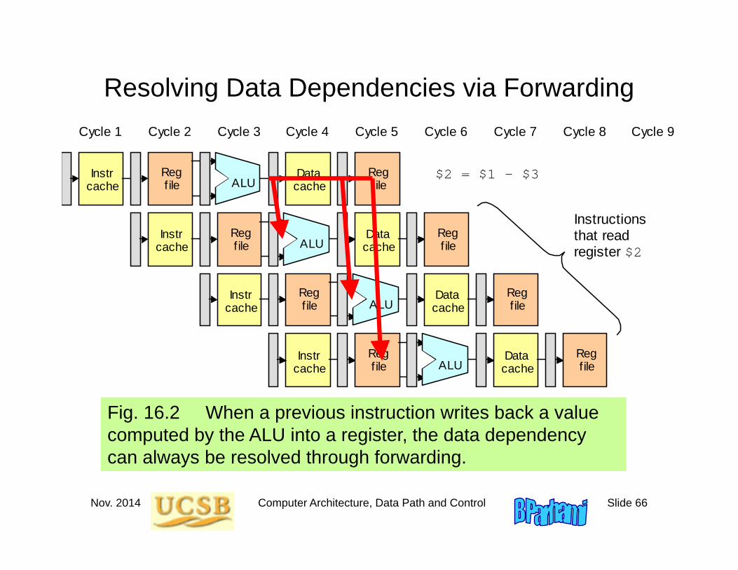
Nov. 2014 Computer Architecture, Data Path and Control Slide 66
Fig. 16.2 When a previous instruction writes back a value computed by the ALU into a register, the data dependency can always be resolved through forwarding.
Resolving Data Dependencies via Forwarding Cycle 7 Cycle 6 Cycle 5 Cycle 4 Cycle 3 Cycle 2 Cycle 1 Cycle 8
Reg f ile
Reg f ile ALU
Reg f ile
Reg f ile ALU
Reg file
Reg file ALU
Reg f ile
Reg file ALU
Cycle 9
$2 = $1 - $3
Instructions that read register $2
Instr cache
Instr cache
Instr cache
Instr cache
Data cache
Data cache
Data cache
Data cache
Nov. 2014 Computer Architecture, Data Path and Control Slide 67
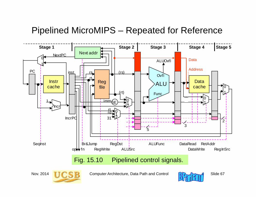
Pipelined MicroMIPS – Repeated for Reference
Fig. 15.10 Pipelined control signals. ALU
Data
cache Instr
cache
Next addr
Reg file
op fn
inst
imm
rs (rs)
(rt)
Data addr
ALUSrc ALUFunc
DataWrite DataRead
RegInSrc
rt
rd
RegDst RegWrite
Func
ALUOvfl
Ovfl
IncrPC
Br&Jump
PC
1 Incr
0 1
rt
31
0 1 2
NextPC
0 1
SeqInst
0 1 2
0 1
RetAddr
Stage 1 Stage 2 Stage 3 Stage 4 Stage 5
SE
5 3
2
Address
Data
Nov. 2014 Computer Architecture, Data Path and Control Slide 68
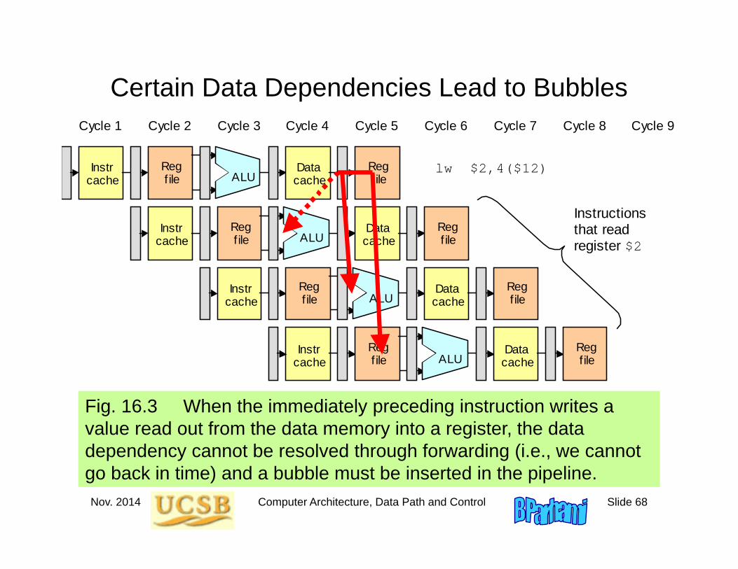
Fig. 16.3 When the immediately preceding instruction writes a value read out from the data memory into a register, the data dependency cannot be resolved through forwarding (i.e., we cannot go back in time) and a bubble must be inserted in the pipeline.
Certain Data Dependencies Lead to Bubbles Cycle 7 Cycle 6 Cycle 5 Cycle 4 Cycle 3 Cycle 2 Cycle 1 Cycle 8
Reg f ile
Reg f ile ALU
Reg f ile
Reg f ile ALU
Reg file
Reg file ALU
Reg f ile
Reg file ALU
Cycle 9
lw $2,4($12)
Instructions that read register $2
Instr cache
Instr cache
Instr cache
Instr cache
Data cache
Data cache
Data cache
Data cache
Nov. 2014 Computer Architecture, Data Path and Control Slide 69
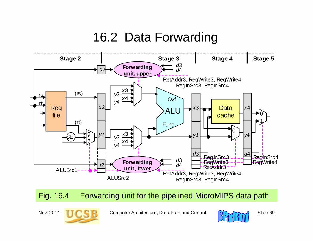
16.2 Data Forwarding
Fig. 16.4 Forwarding unit for the pipelined MicroMIPS data path.
(rt)
0 1 2
SE
ALU
Data cache
RegInSrc4
Func
Ovfl
0 1
0 1
RegWrite4 RetAddr3
(rs)
ALUSrc1
Stage 3 Stage 4 Stage 5 Stage 2
x3
y3
x4
y4 x3 y3 x4
y4
RegWrite3 d3 d4
x3 y3
x4 y4
Reg file
rs rt
RegInSrc3
ALUSrc2
s2
t2
d4 d3
RetAddr3, RegWrite3, RegWrite4 RegInSrc3, RegInSrc4
RetAddr3, RegWrite3, RegWrite4 RegInSrc3, RegInSrc4
d4 d3
Forwarding unit, upper
Forwarding unit, lower
x2
y2
Nov. 2014 Computer Architecture, Data Path and Control Slide 70
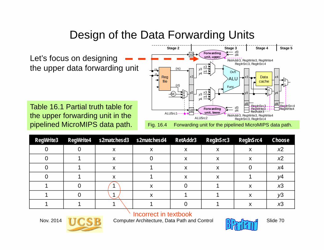
Design of the Data Forwarding Units
Fig. 16.4 Forwarding unit for the pipelined MicroMIPS data path.
(rt)
0 1 2
SE
ALU
Data cache
RegInSrc4
Func
Ovfl
0 1
0 1
RegWrite4 RetAddr3
(rs)
ALUSrc1
Stage 3 Stage 4 Stage 5 Stage 2
x3
y3
x4
y4 x3 y3 x4
y4
RegWrite3 d3 d4
x3 y3
x4 y4
Reg file
rs rt
RegInSrc3
ALUSrc2
s2
t2
d4 d3
RetAddr3, RegWrite3, RegWrite4 RegInSrc3, RegInSrc4
RetAddr3, RegWrite3, RegWrite4 RegInSrc3, RegInSrc4
d4 d3
Forwarding unit, upper
Forwarding unit, lower
x2
y2
RegWrite3 RegWrite4 s2matchesd3 s2matchesd4 RetAddr3 RegInSrc3 RegInSrc4 Choose0 0 x x x x x x20 1 x 0 x x x x20 1 x 1 x x 0 x40 1 x 1 x x 1 y41 0 1 x 0 1 x x31 0 1 x 1 1 x y31 1 1 1 0 1 x x3
Table 16.1 Partial truth table for the upper forwarding unit in the pipelined MicroMIPS data path.
Let’s focus on designing the upper data forwarding unit
Incorrect in textbook

Nov. 2014 Computer Architecture, Data Path and Control Slide 71
Hardware for Inserting Bubbles
Fig. 16.5 Data hazard detector for the pipelined MicroMIPS data path.
(rt)
0 1 2
(rs)
Stage 3 Stage 2
Reg file
rs rt
t2
Data hazard detector
x2
y2
Control signals from decoder
DataRead2
Instr cache
LoadPC
Stage 1
PC Inst reg
All-0s
0 1
Bubble
Controls or all-0s
Inst
IncrPC
LoadInst
LoadIncrPC
Corrections to textbook figure shown in red
Nov. 2014 Computer Architecture, Data Path and Control Slide 72
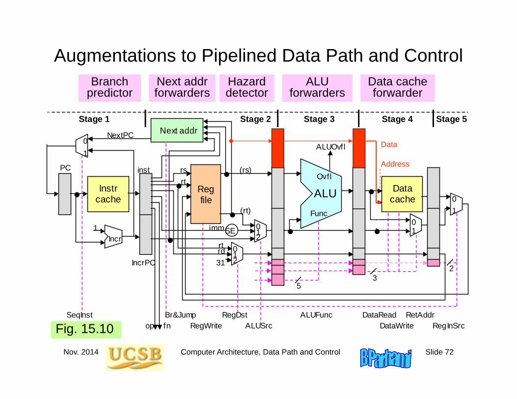
Augmentations to Pipelined Data Path and Control
Fig. 15.10 ALU
Data
cache Instr
cache
Next addr
Reg file
op fn
inst
imm
rs (rs)
(rt)
Data addr
ALUSrc ALUFunc
DataWrite DataRead
RegInSrc
rt
rd
RegDst RegWrite
Func
ALUOvfl
Ovfl
IncrPC
Br&Jump
PC
1 Incr
0 1
rt
31
0 1 2
NextPC
0 1
SeqInst
0 1 2
0 1
RetAddr
Stage 1 Stage 2 Stage 3 Stage 4 Stage 5
SE
5 3
2
Address
Data
ALU forwarders
Hazard detector
Data cache forwarder
Next addr forwarders
Branch predictor
Nov. 2014 Computer Architecture, Data Path and Control Slide 73
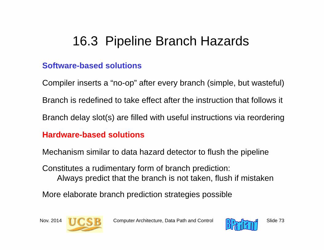
16.3 Pipeline Branch Hazards
Software-based solutions
Compiler inserts a “no-op” after every branch (simple, but wasteful)
Branch is redefined to take effect after the instruction that follows it
Branch delay slot(s) are filled with useful instructions via reordering
Hardware-based solutions
Mechanism similar to data hazard detector to flush the pipeline
Constitutes a rudimentary form of branch prediction:Always predict that the branch is not taken, flush if mistaken
More elaborate branch prediction strategies possible
Nov. 2014 Computer Architecture, Data Path and Control Slide 74
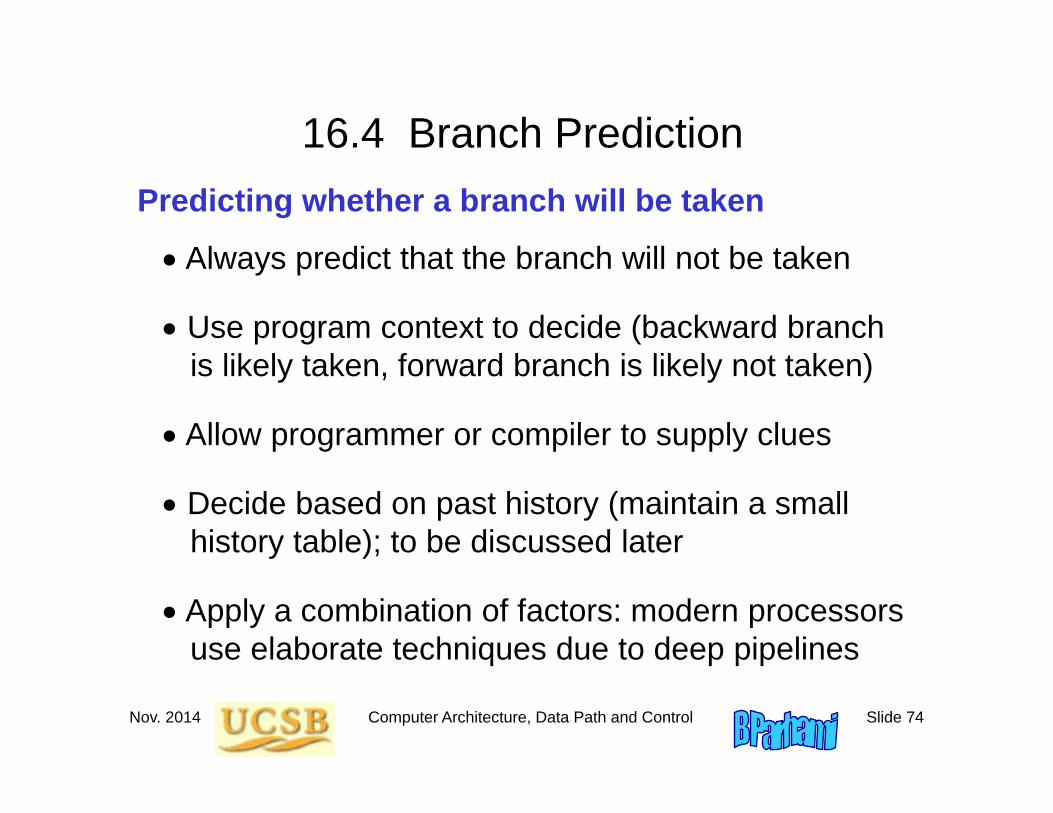
16.4 Branch PredictionPredicting whether a branch will be taken
Always predict that the branch will not be taken
Use program context to decide (backward branch is likely taken, forward branch is likely not taken)
Allow programmer or compiler to supply clues
Decide based on past history (maintain a small history table); to be discussed later
Apply a combination of factors: modern processorsuse elaborate techniques due to deep pipelines

Nov. 2014 Computer Architecture, Data Path and Control Slide 75
Forward and Backward Branches
List A is stored in memory beginning at the address given in $s1. List length is given in $s2. Find the largest integer in the list and copy it into $t0.
Solution
Scan the list, holding the largest element identified thus far in $t0.lw $t0,0($s1) # initialize maximum to A[0]addi $t1,$zero,0 # initialize index i to 0
loop: add $t1,$t1,1 # increment index i by 1beq $t1,$s2,done # if all elements examined, quitadd $t2,$t1,$t1 # compute 2i in $t2add $t2,$t2,$t2 # compute 4i in $t2add $t2,$t2,$s1 # form address of A[i] in $t2lw $t3,0($t2) # load value of A[i] into $t3slt $t4,$t0,$t3 # maximum < A[i]?beq $t4,$zero,loop # if not, repeat with no changeaddi $t0,$t3,0 # if so, A[i] is the new maximumj loop # change completed; now repeat
done: ... # continuation of the program
Example 5.5

Nov. 2014 Computer Architecture, Data Path and Control Slide 76
Simple Branch Prediction: 1-Bit History
Two-state branch prediction scheme.
Predicttaken
Predictnot taken
Taken
Taken
Not takenNot taken
Problem with this approach:Each branch in a loop entails two mispredictions:
Once in first iteration (loop is repeated, but the history indicates exit from loop)
Once in last iteration (when loop is terminated, but history indicates repetition)
Nov. 2014 Computer Architecture, Data Path and Control Slide 77
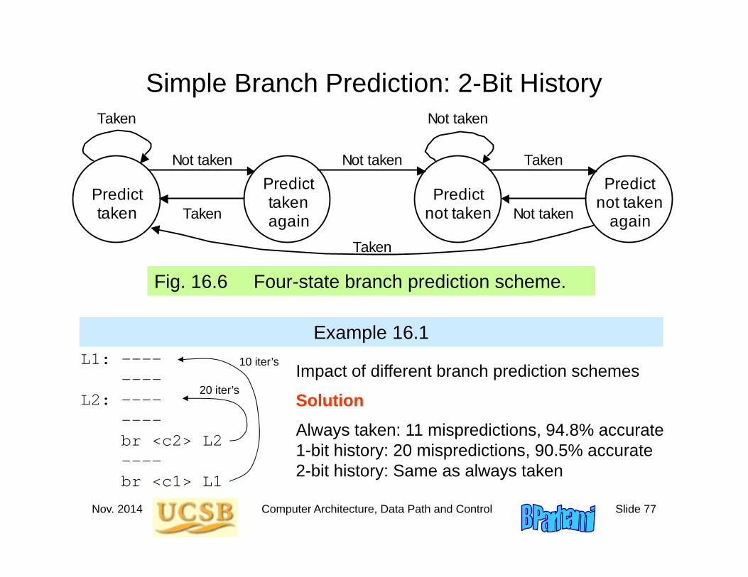
Simple Branch Prediction: 2-Bit History
Fig. 16.6 Four-state branch prediction scheme.
Not taken
Predict taken
Predict taken again
Predict not taken
Predict not taken
again
Not taken Taken
Not taken Taken
Taken Not taken
Taken
Example 16.1L1: ----
----L2: ----
----br <c2> L2----br <c1> L1
20 iter’s
10 iter’s Impact of different branch prediction schemes
SolutionAlways taken: 11 mispredictions, 94.8% accurate1-bit history: 20 mispredictions, 90.5% accurate2-bit history: Same as always taken
Nov. 2014 Computer Architecture, Data Path and Control Slide 78
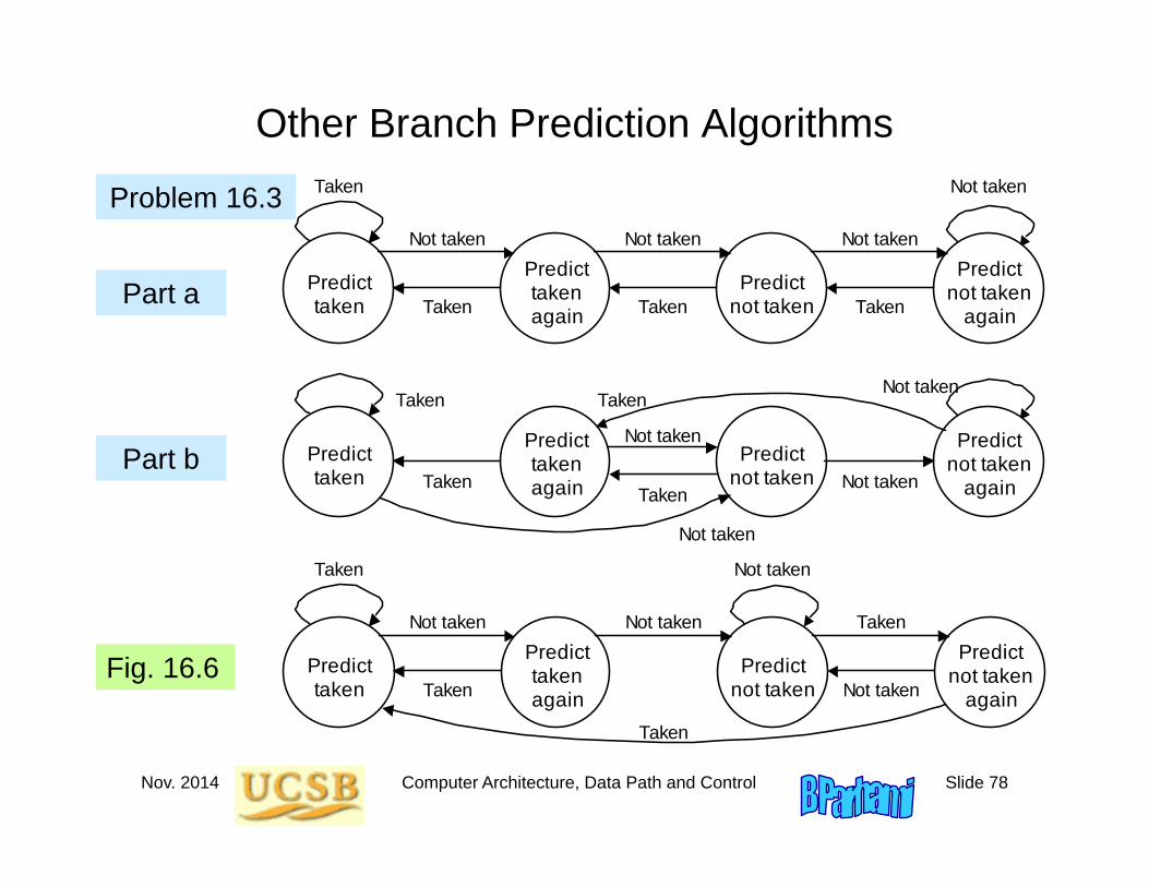
Other Branch Prediction Algorithms
Problem 16.3Not taken
Predict taken
Predict taken again
Predict not taken
Predict not taken
again
Not taken
Taken
Not taken
Taken
Taken Not taken
Taken
Not taken
Predict taken
Predict taken again
Predict not taken
Predict not taken
again
Not taken
Taken
Not taken Taken
Taken Not taken
Taken
Not taken
Predict taken
Predict taken again
Predict not taken
Predict not taken
again
Not taken Taken
Not taken Taken
Taken Not taken
Taken
Fig. 16.6
Part a
Part b
Nov. 2014 Computer Architecture, Data Path and Control Slide 79
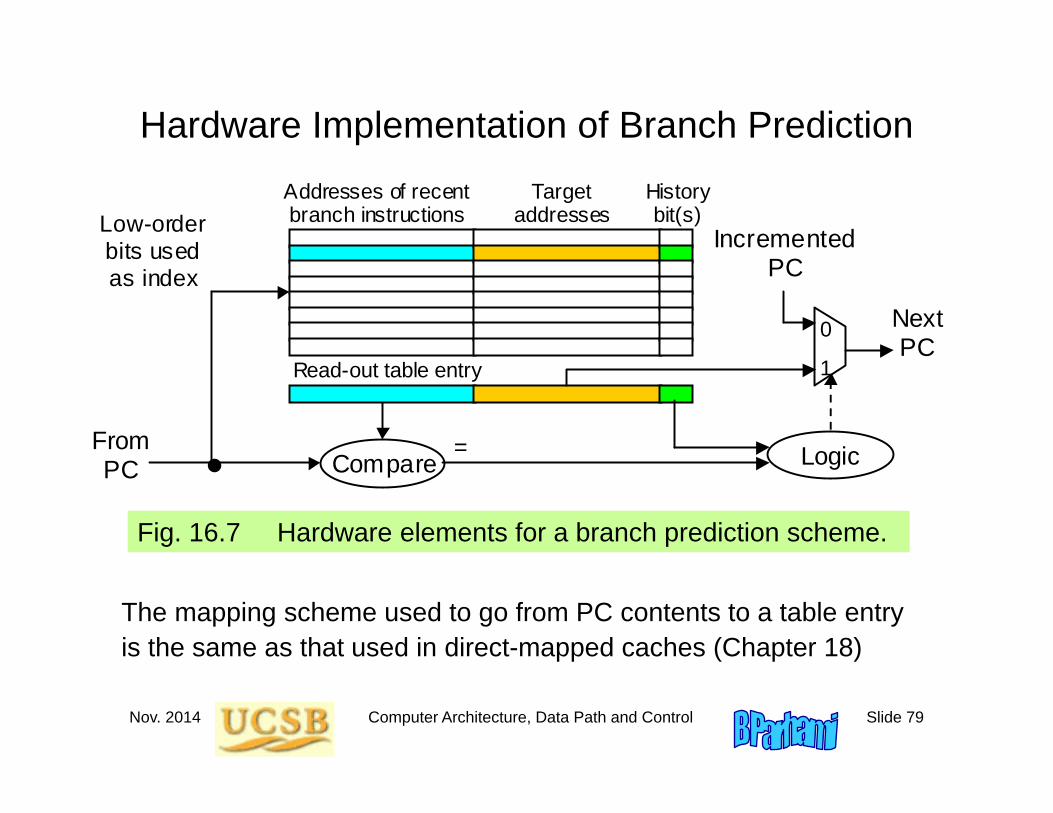
Hardware Implementation of Branch Prediction
Fig. 16.7 Hardware elements for a branch prediction scheme.
The mapping scheme used to go from PC contents to a table entry is the same as that used in direct-mapped caches (Chapter 18)
Compare
Addresses of recent branch instructions
Target addresses
History bit(s) Low-order
bits used as index
Logic From PC
Incremented PC
Next PC
0
1
=
Read-out table entry

Nov. 2014 Computer Architecture, Data Path and Control Slide 80
Pipeline Augmentations – Repeated for Reference
Fig. 15.10 ALU
Data
cache Instr
cache
Next addr
Reg file
op fn
inst
imm
rs (rs)
(rt)
Data addr
ALUSrc ALUFunc
DataWrite DataRead
RegInSrc
rt
rd
RegDst RegWrite
Func
ALUOvfl
Ovfl
IncrPC
Br&Jump
PC
1 Incr
0 1
rt
31
0 1 2
NextPC
0 1
SeqInst
0 1 2
0 1
RetAddr
Stage 1 Stage 2 Stage 3 Stage 4 Stage 5
SE
5 3
2
Address
Data
ALU forwarders
Hazard detector
Data cache forwarder
Next addr forwarders
Branch predictor
Nov. 2014 Computer Architecture, Data Path and Control Slide 81
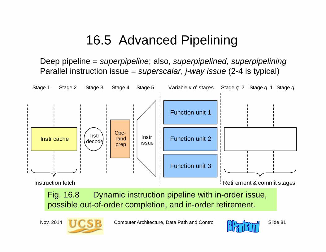
16.5 Advanced Pipelining
Fig. 16.8 Dynamic instruction pipeline with in-order issue, possible out-of-order completion, and in-order retirement.
Deep pipeline = superpipeline; also, superpipelined, superpipeliningParallel instruction issue = superscalar, j-way issue (2-4 is typical)
Stage 1
Instr cache
Instruction fetch
Function unit 1
Function unit 2
Function unit 3
Stage 2 Stage 3 Stage 4 Variable # of stages Stage q2 Stage q1 Stage q
Ope- rand prep
Instr decode
Retirement & commit stages
Instr issue
Stage 5
Nov. 2014 Computer Architecture, Data Path and Control Slide 82
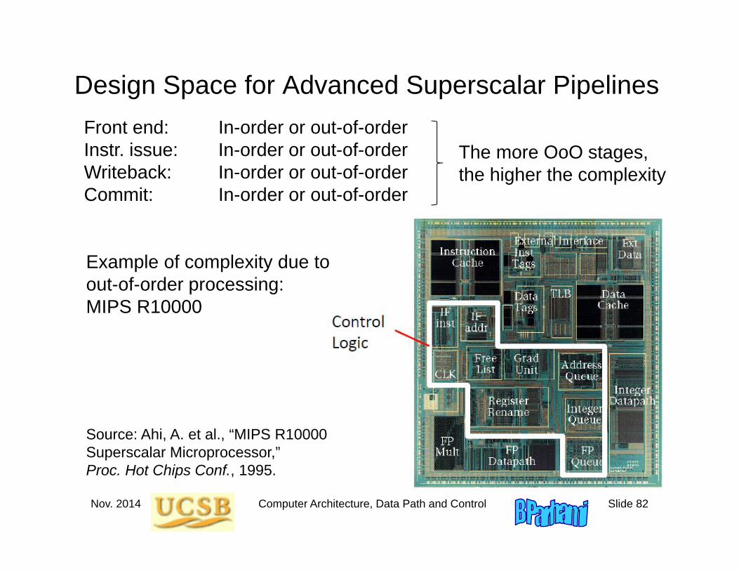
Design Space for Advanced Superscalar PipelinesFront end: In-order or out-of-orderInstr. issue: In-order or out-of-orderWriteback: In-order or out-of-orderCommit: In-order or out-of-order
The more OoO stages,the higher the complexity
Example of complexity due toout-of-order processing: MIPS R10000
Source: Ahi, A. et al., “MIPS R10000Superscalar Microprocessor,”Proc. Hot Chips Conf., 1995.
Nov. 2014 Computer Architecture, Data Path and Control Slide 83
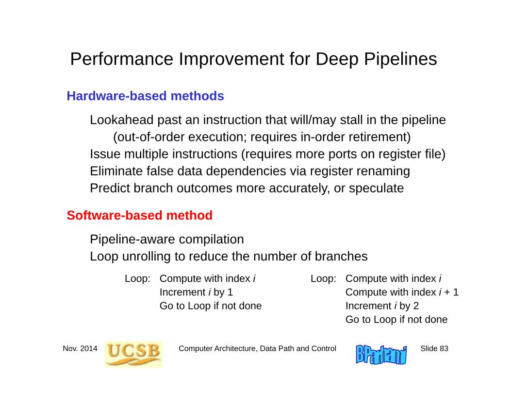
Performance Improvement for Deep Pipelines
Hardware-based methods
Lookahead past an instruction that will/may stall in the pipeline(out-of-order execution; requires in-order retirement)
Issue multiple instructions (requires more ports on register file)Eliminate false data dependencies via register renamingPredict branch outcomes more accurately, or speculate
Software-based method
Pipeline-aware compilationLoop unrolling to reduce the number of branches
Loop: Compute with index i Loop: Compute with index iIncrement i by 1 Compute with index i + 1Go to Loop if not done Increment i by 2
Go to Loop if not done

Nov. 2014 Computer Architecture, Data Path and Control Slide 84
CPI Variations with Architectural Features
Table 16.2 Effect of processor architecture, branch prediction methods, and speculative execution on CPI.
Architecture Methods used in practice CPINonpipelined, multicycle Strict in-order instruction issue and exec 5-10
Nonpipelined, overlapped In-order issue, with multiple function units 3-5
Pipelined, static In-order exec, simple branch prediction 2-3
Superpipelined, dynamic Out-of-order exec, adv branch prediction 1-2
Superscalar 2- to 4-way issue, interlock & speculation 0.5-1
Advanced superscalar 4- to 8-way issue, aggressive speculation 0.2-0.5
3.3 inst / cycle 3 Gigacycles / s 10 GIPS
Need 100 for TIPS performanceNeed 100,000 for 1 PIPS

Nov. 2014 Computer Architecture, Data Path and Control Slide 85
Development of Intel’s Desktop/Laptop Micros
In the beginning, there was the 8080; led to the 80x86 = IA32 ISA
Half a dozen or so pipeline stages
802868038680486Pentium (80586)
A dozen or so pipeline stages, with out-of-order instruction execution
Pentium ProPentium IIPentium IIICeleron
Two dozens or so pipeline stages
Pentium 4
More advanced technology
More advanced technology
Instructions are broken into micro-ops which are executed out-of-order but retired in-order

Nov. 2014 Computer Architecture, Data Path and Control Slide 86
Current State of Computer Performance
Multi-GIPS/GFLOPS desktops and laptops
Very few users need even greater computing powerUsers unwilling to upgrade just to get a faster processorCurrent emphasis on power reduction and ease of use
Multi-TIPS/TFLOPS in large computer centers
World’s top 500 supercomputers, http://www.top500.org Next list due in June 2009; as of Nov. 2008:All 500 >> 10 TFLOPS, 30 > 100 TFLOPS, 1 > PFLOPS
Multi-PIPS/PFLOPS supercomputers on the drawing board
IBM “smarter planet” TV commercial proclaims (in early 2009):“We just broke the petaflop [sic] barrier.”The technical term “petaflops” is now in the public sphere
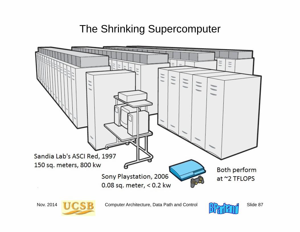
Nov. 2014 Computer Architecture, Data Path and Control Slide 87
The Shrinking Supercomputer
Nov. 2014 Computer Architecture, Data Path and Control Slide 88
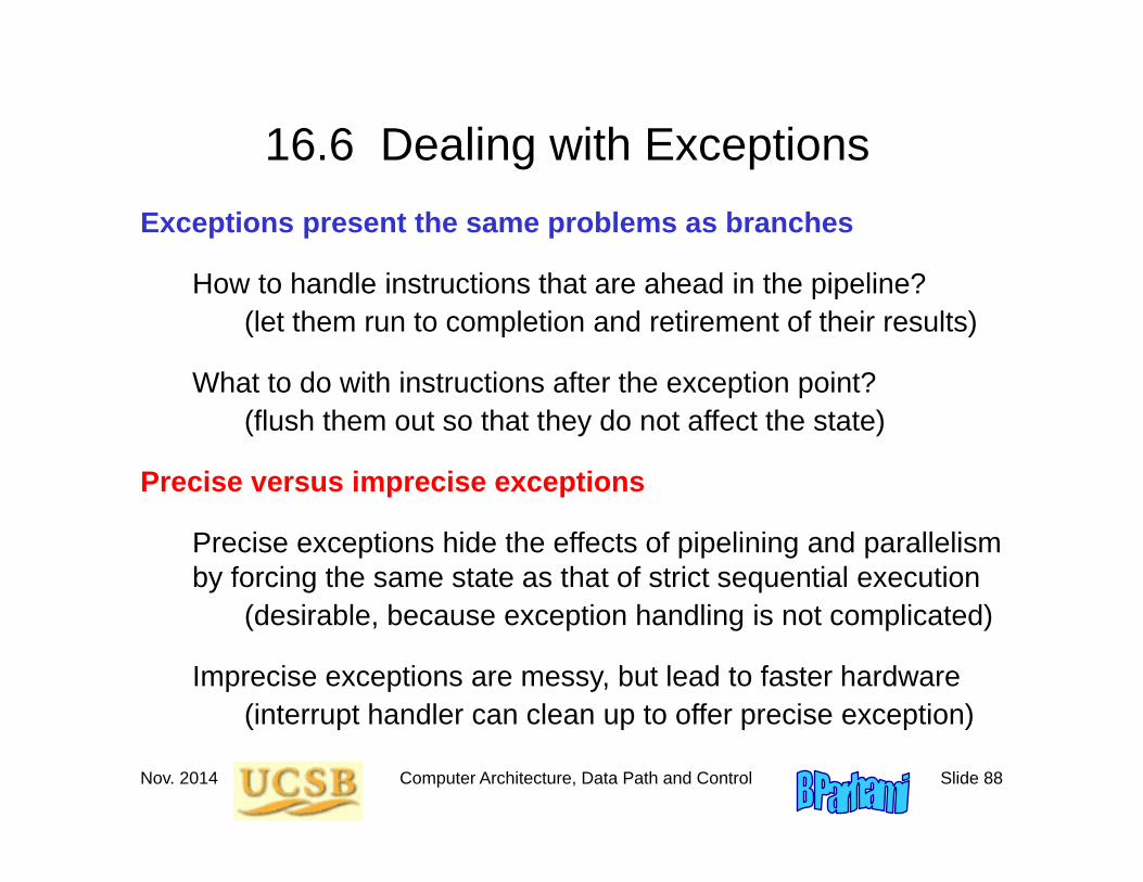
16.6 Dealing with ExceptionsExceptions present the same problems as branches
How to handle instructions that are ahead in the pipeline?(let them run to completion and retirement of their results)
What to do with instructions after the exception point?(flush them out so that they do not affect the state)
Precise versus imprecise exceptions
Precise exceptions hide the effects of pipelining and parallelism by forcing the same state as that of strict sequential execution
(desirable, because exception handling is not complicated)
Imprecise exceptions are messy, but lead to faster hardware(interrupt handler can clean up to offer precise exception)
Nov. 2014 Computer Architecture, Data Path and Control Slide 89
The Three Hardware Designs for MicroMIPS
/
ALU
Data cache
Instr cache
Next addr
Reg file
op
jta
fn
inst
imm
rs (rs)
(rt)
Data addr
Data in 0
1
ALUSrc ALUFunc DataWrite
DataRead
SE
RegInSrc
rt
rd
RegDst RegWrite
32 / 16
Register input
Data out
Func
ALUOvfl
Ovfl
31
0 1 2
Next PC
Incr PC
(PC)
Br&Jump
ALU out
PC
0 1 2
Single-cycle
/
16
rs
0 1
0 1 2
ALU
Cache Reg file
op
jta
fn
(rs)
(rt)
Address
Data
Inst Reg
Data Reg
x Reg
y Reg
z Reg PC
4
ALUSrcX
ALUFunc
MemWrite MemRead
RegInSrc
4
rd
RegDst RegWrite
/
32
Func
ALUOvfl
Ovf l
31
PCSrc PCWrite IRWrite
ALU out
0 1
0 1
0 1 2 3
0 1 2 3
InstData ALUSrcY
SysCallAddr
/
26
4
rt
ALUZero
Zero
x Mux
y Mux
0 1
JumpAddr
4 MSBs
/
30
30
SE
imm
Multicycle
125 MHzCPI = 1
500 MHzCPI 4
500 MHzCPI 1.1
ALU
Data cache
Instr cache
Next addr
Reg file
op fn
inst
imm
rs (rs)
(rt)
Data addr
ALUSrc A LUFunc
DataWrite DataRead
Reg InSrc
rt
rd
RegDst RegWrite
Func
ALUOvf l
Ovf l
IncrPC
Br&Jump
PC
1 Incr
0 1
rt
31
0 1 2
NextPC
0 1
SeqInst
0 1 2
0 1
RetAddr
Stage 1 Stage 2 Stage 3 Stage 4 Stage 5
SE
5 3
2
Address
Data

Nov. 2014 Computer Architecture, Data Path and Control Slide 90
Where Do We Go from Here?
Memory Design: How to build a memory unitthat responds in 1 clock
Input and Output:Peripheral devices, I/O programming,interfacing, interrupts
Higher Performance:Vector/array processingParallel processing