D C a n d A C S w i t c h i n g C h a r a c t e r i s t i ...
81
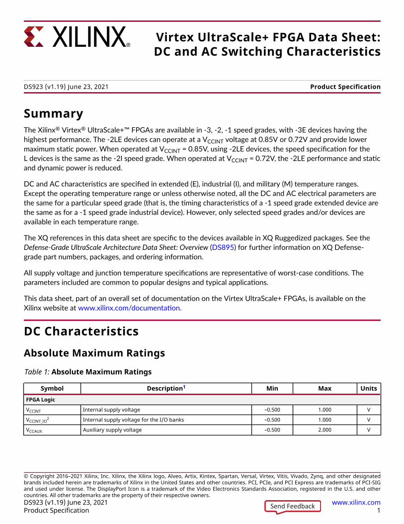
Summary The Xilinx ® Virtex ® UltraScale+™ FPGAs are available in -3, -2, -1 speed grades, with -3E devices having the highest performance. The -2LE devices can operate at a V CCINT voltage at 0.85V or 0.72V and provide lower maximum stac power. When operated at V CCINT = 0.85V, using -2LE devices, the speed specificaon for the L devices is the same as the -2I speed grade. When operated at V CCINT = 0.72V, the -2LE performance and stac and dynamic power is reduced. DC and AC characteriscs are specified in extended (E), industrial (I), and military (M) temperature ranges. Except the operang temperature range or unless otherwise noted, all the DC and AC electrical parameters are the same for a parcular speed grade (that is, the ming characteriscs of a -1 speed grade extended device are the same as for a -1 speed grade industrial device). However, only selected speed grades and/or devices are available in each temperature range. The XQ references in this data sheet are specific to the devices available in XQ Ruggedized packages. See the Defense-Grade UltraScale Architecture Data Sheet: Overview (DS895) for further informaon on XQ Defense- grade part numbers, packages, and ordering informaon. All supply voltage and juncon temperature specificaons are representave of worst-case condions. The parameters included are common to popular designs and typical applicaons. This data sheet, part of an overall set of documentaon on the Virtex UltraScale+ FPGAs, is available on the Xilinx website at www.xilinx.com/documentaon. DC Characteristics Absolute Maximum Ratings Table 1: Absolute Maximum Ratings Symbol Description 1 Min Max Units FPGA Logic V CCINT Internal supply voltage –0.500 1.000 V V CCINT_IO 2 Internal supply voltage for the I/O banks –0.500 1.000 V V CCAUX Auxiliary supply voltage –0.500 2.000 V Virtex UltraScale+ FPGA Data Sheet: DC and AC Switching Characteristics DS923 (v1.19) June 23, 2021 Product Specification © Copyright 2016–2021 Xilinx, Inc. Xilinx, the Xilinx logo, Alveo, Artix, Kintex, Spartan, Versal, Virtex, Vitis, Vivado, Zynq, and other designated brands included herein are trademarks of Xilinx in the United States and other countries. PCI, PCIe, and PCI Express are trademarks of PCI-SIG and used under license. The DisplayPort Icon is a trademark of the Video Electronics Standards Association, registered in the U.S. and other countries. All other trademarks are the property of their respective owners. DS923 (v1.19) June 23, 2021 www.xilinx.com Product Specification 1
Transcript of D C a n d A C S w i t c h i n g C h a r a c t e r i s t i ...
SummaryThe Xilinx® Virtex® UltraScale+™ FPGAs are available in -3, -2, -1 speed grades, with -3E devices having thehighest performance. The -2LE devices can operate at a VCCINT voltage at 0.85V or 0.72V and provide lowermaximum static power. When operated at VCCINT = 0.85V, using -2LE devices, the speed specification for theL devices is the same as the -2I speed grade. When operated at VCCINT = 0.72V, the -2LE performance and staticand dynamic power is reduced.
DC and AC characteristics are specified in extended (E), industrial (I), and military (M) temperature ranges.Except the operating temperature range or unless otherwise noted, all the DC and AC electrical parameters arethe same for a particular speed grade (that is, the timing characteristics of a -1 speed grade extended device arethe same as for a -1 speed grade industrial device). However, only selected speed grades and/or devices areavailable in each temperature range.
The XQ references in this data sheet are specific to the devices available in XQ Ruggedized packages. See theDefense-Grade UltraScale Architecture Data Sheet: Overview (DS895) for further information on XQ Defense-grade part numbers, packages, and ordering information.
All supply voltage and junction temperature specifications are representative of worst-case conditions. Theparameters included are common to popular designs and typical applications.
This data sheet, part of an overall set of documentation on the Virtex UltraScale+ FPGAs, is available on theXilinx website at www.xilinx.com/documentation.
DC CharacteristicsAbsolute Maximum RatingsTable 1: Absolute Maximum Ratings
Symbol Description1 Min Max UnitsFPGA Logic
VCCINT Internal supply voltage –0.500 1.000 V
VCCINT_IO2 Internal supply voltage for the I/O banks –0.500 1.000 V
VCCAUX Auxiliary supply voltage –0.500 2.000 V
Virtex UltraScale+ FPGA Data Sheet:DC and AC Switching Characteristics
DS923 (v1.19) June 23, 2021 Product Specification
© Copyright 2016–2021 Xilinx, Inc. Xilinx, the Xilinx logo, Alveo, Artix, Kintex, Spartan, Versal, Virtex, Vitis, Vivado, Zynq, and other designatedbrands included herein are trademarks of Xilinx in the United States and other countries. PCI, PCIe, and PCI Express are trademarks of PCI-SIGand used under license. The DisplayPort Icon is a trademark of the Video Electronics Standards Association, registered in the U.S. and othercountries. All other trademarks are the property of their respective owners.DS923 (v1.19) June 23, 2021 www.xilinx.comProduct Specification 1Send Feedback
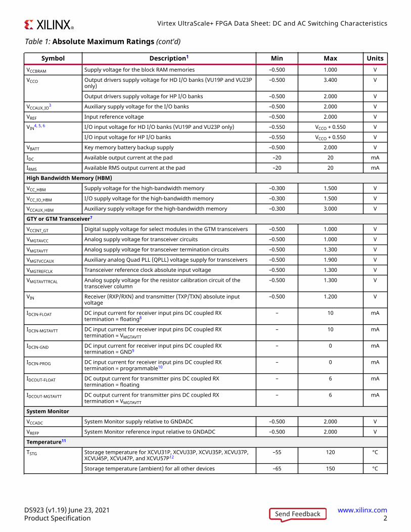
Table 1: Absolute Maximum Ratings (cont'd)
Symbol Description1 Min Max UnitsVCCBRAM Supply voltage for the block RAM memories –0.500 1.000 V
VCCO Output drivers supply voltage for HD I/O banks (VU19P and VU23Ponly)
–0.500 3.400 V
Output drivers supply voltage for HP I/O banks –0.500 2.000 V
VCCAUX_IO3 Auxiliary supply voltage for the I/O banks –0.500 2.000 V
VREF Input reference voltage –0.500 2.000 V
VIN4, 5, 6 I/O input voltage for HD I/O banks (VU19P and VU23P only) –0.550 VCCO + 0.550 V
I/O input voltage for HP I/O banks –0.550 VCCO + 0.550 V
VBATT Key memory battery backup supply –0.500 2.000 V
IDC Available output current at the pad –20 20 mA
IRMS Available RMS output current at the pad –20 20 mA
High Bandwidth Memory (HBM)
VCC_HBM Supply voltage for the high-bandwidth memory –0.300 1.500 V
VCC_IO_HBM I/O supply voltage for the high-bandwidth memory –0.300 1.500 V
VCCAUX_HBM Auxiliary supply voltage for the high-bandwidth memory –0.300 3.000 V
GTY or GTM Transceiver7
VCCINT_GT Digital supply voltage for select modules in the GTM transceivers –0.500 1.000 V
VMGTAVCC Analog supply voltage for transceiver circuits –0.500 1.000 V
VMGTAVTT Analog supply voltage for transceiver termination circuits –0.500 1.300 V
VMGTVCCAUX Auxiliary analog Quad PLL (QPLL) voltage supply for transceivers –0.500 1.900 V
VMGTREFCLK Transceiver reference clock absolute input voltage –0.500 1.300 V
VMGTAVTTRCAL Analog supply voltage for the resistor calibration circuit of thetransceiver column
–0.500 1.300 V
VIN Receiver (RXP/RXN) and transmitter (TXP/TXN) absolute inputvoltage
–0.500 1.200 V
IDCIN-FLOAT DC input current for receiver input pins DC coupled RXtermination = floating8
– 10 mA
IDCIN-MGTAVTT DC input current for receiver input pins DC coupled RXtermination = VMGTAVTT
– 10 mA
IDCIN-GND DC input current for receiver input pins DC coupled RXtermination = GND9
– 0 mA
IDCIN-PROG DC input current for receiver input pins DC coupled RXtermination = programmable10
– 0 mA
IDCOUT-FLOAT DC output current for transmitter pins DC coupled RXtermination = floating
– 6 mA
IDCOUT-MGTAVTT DC output current for transmitter pins DC coupled RXtermination = VMGTAVTT
– 6 mA
System Monitor
VCCADC System Monitor supply relative to GNDADC –0.500 2.000 V
VREFP System Monitor reference input relative to GNDADC –0.500 2.000 V
Temperature11
TSTG Storage temperature for XCVU31P, XCVU33P, XCVU35P, XCVU37P,XCVU45P, XCVU47P, and XCVU57P12
–55 120 °C
Storage temperature (ambient) for all other devices –65 150 °C
Virtex UltraScale+ FPGA Data Sheet: DC and AC Switching Characteristics
DS923 (v1.19) June 23, 2021 www.xilinx.comProduct Specification 2Send Feedback

Table 1: Absolute Maximum Ratings (cont'd)
Symbol Description1 Min Max UnitsTSOL Maximum dry rework soldering temperature – 260 °C
Maximum reflow soldering temperature for FFVC1517, FLGF1924,FHGA2104, FHGB2104, FHGC2104, FLGA2104, FLGB2104, FLGC2104,FLVA2104, FLVB2104, FLVC2104, FLGA2577
– 245 °C
Maximum reflow soldering temperature for lidless packages withstiffener ring (VSVA1365, FSVJ1760, FIGD2104, FSGD2104,FSVH1924, FSVH2104, FSGA2577, FSVH2892, FSVK2892, FSVA3824,FSVB3824)
– 240 °C
Maximum reflow soldering temperature for the FFRC1517,FFRA2104, FFRB2104, and FFRC2104 packages
– 225 °C
Tj Maximum junction temperature for XCVU31P, XCVU33P, XCVU35P,XCVU37P, XCVU45P, XCVU47P, and XCVU57P
– 120 °C
Maximum junction temperature for all other devices – 125 °C
Notes:1. Stresses beyond those listed under Absolute Maximum Ratings might cause permanent damage to the device. These are stress ratings
only, and functional operation of the device at these or any other conditions beyond those listed under Operating Conditions is notimplied. Exposure to Absolute Maximum Ratings conditions for extended periods of time might affect device reliability.
2. VCCINT_IO must be connected to VCCBRAM.3. VCCAUX_IO must be connected to VCCAUX.4. The lower absolute voltage specification always applies.5. For I/O operation, see the UltraScale Architecture SelectIO Resources User Guide (UG571).6. When operating outside of the recommended operating conditions, refer to Table 4 and Table 5 for maximum overshoot and
undershoot specifications.7. For more information on supported GTY transceiver terminations see the UltraScale Architecture GTY Transceivers User Guide (UG578) or
Virtex UltraScale+ FPGAs GTM Transceivers User Guide (UG581).8. AC coupled operation is not supported for RX termination = floating.9. For GTY transceivers, DC coupled operation is not supported for RX termination = GND.10. DC coupled operation is not supported for RX termination = programmable.11. For soldering guidelines and thermal considerations, see the UltraScale and UltraScale+ FPGAs Packaging and Pinouts Product Specification
(UG575).12. For devices with high-bandwidth memory (HBM), the storage temperature is the case surface temperature on the center/top side of the
device. For the measurement conditions, refer to the JESD51-2 standard.
Recommended Operating ConditionsTable 2: Recommended Operating Conditions
Symbol Description1, 2 Min Typ Max UnitsFPGA Logic
VCCINT Internal supply voltage 0.825 0.850 0.876 V
For -2LE (VCCINT = 0.72V) devices: internal supply voltage 0.698 0.720 0.742 V
For -3E devices: internal supply voltage 0.873 0.900 0.927 V
VCCINT_IO3 Internal supply voltage for the I/O banks 0.825 0.850 0.876 V
For -2LE (VCCINT = 0.72V) devices: internal supply voltage for theI/O banks
0.825 0.850 0.876 V
For -3E devices: internal supply voltage for the I/O banks 0.873 0.900 0.927 V
VCCBRAM Block RAM supply voltage 0.825 0.850 0.876 V
For -3E devices: block RAM supply voltage 0.873 0.900 0.927 V
VCCAUX Auxiliary supply voltage 1.746 1.800 1.854 V
Virtex UltraScale+ FPGA Data Sheet: DC and AC Switching Characteristics
DS923 (v1.19) June 23, 2021 www.xilinx.comProduct Specification 3Send Feedback

Table 2: Recommended Operating Conditions (cont'd)
Symbol Description1, 2 Min Typ Max UnitsVCCO4, 5 Supply voltage for HD I/O banks (VU19P and VU23P only) 1.140 – 3.400 V
Supply voltage for HP I/O banks 0.950 – 1.900 V
VCCAUX_IO6 Auxiliary I/O supply voltage 1.746 1.800 1.854 V
VIN7 I/O input voltage –0.200 – VCCO + 0.200 V
IIN8 Maximum current through any pin in a powered or unpoweredbank when forward biasing the clamp diode
– – 10 mA
VBATT9 Battery voltage 1.000 – 1.890 V
High Bandwidth Memory
VCC_HBM Supply voltage for the high-bandwidth memory (HBM) 1.164 1.200 1.236 V
VCC_IO_HBM I/O supply voltage for the high-bandwidth memory 1.164 1.200 1.236 V
VCCAUX_HBM Auxiliary supply voltage for the high-bandwidth memory 2.425 2.500 2.575 V
GTY or GTM Transceiver
VCCINT_GT Digital supply voltage for select modules in the GTMtransceivers
0.825 0.850 0.876 V
For -3E devices: Digital supply voltage for select modules in theGTM transceivers supply voltage
0.873 0.900 0.927 V
VMGTAVCC10 Analog supply voltage for the GTY or GTM transceiver 0.873 0.900 0.927 V
VMGTAVTT10 Analog supply voltage for the GTY or GTM transmitter andreceiver termination circuits
1.164 1.200 1.236 V
VMGTVCCAUX10 Auxiliary analog QPLL voltage supply for the transceivers 1.746 1.800 1.854 V
VMGTAVTTRCAL10 Analog supply voltage for the resistor calibration circuit of theGTY or GTM transceiver column
1.164 1.200 1.236 V
System Monitor
VCCADC System Monitor supply relative to GNDADC 1.746 1.800 1.854 V
VREFP System Monitor externally supplied reference voltage relative toGNDADC
1.200 1.250 1.300 V
Virtex UltraScale+ FPGA Data Sheet: DC and AC Switching Characteristics
DS923 (v1.19) June 23, 2021 www.xilinx.comProduct Specification 4Send Feedback

Table 2: Recommended Operating Conditions (cont'd)
Symbol Description1, 2 Min Typ Max UnitsTemperature
Tj11 Junction temperature operating range for XCVU31P, XCVU33P,XCVU35P, and XCVU37P, XCVU45P, XCVU47P, XCVU57P extended(E) temperature devices12, 13, 14
0 – 100 °C
Junction temperature operating range for all other extended (E)temperature devices12
0 – 100 °C
Junction temperature operating range for industrial (I)temperature devices
–40 – 100 °C
Junction temperature operating range for eFUSE programming15 –40 – 125 °C
Notes:1. All voltages are relative to GND.2. For the design of the power distribution system consult the UltraScale Architecture PCB Design User Guide (UG583).3. VCCINT_IO must be connected to VCCBRAM.4. For VCCO_0, the minimum recommended operating voltage for power on and during configuration is 1.425V. After configuration, data is
retained even if VCCO drops to 0V.5. Includes VCCO of 1.0V (HP I/O only), 1.2V, 1.35V, 1.5V, 1.8V, 2.5V (HD I/O only) at ±5%, and 3.3V (HD I/O only) at +3/–5%.6. VCCAUX_IO must be connected to VCCAUX.7. The lower absolute voltage specification always applies.8. A total of 200 mA per bank should not be exceeded.9. If battery is not used, connect VBATT to either GND or VCCAUX.10. Each voltage listed requires filtering as described in the UltraScale Architecture GTY Transceivers User Guide (UG578) or the Virtex UltraScale
+ FPGAs GTM Transceivers User Guide (UG581).11. Xilinx recommends measuring the Tj of a device using the system monitor as described in the UltraScale Architecture System Monitor User
Guide (UG580). The system monitor temperature measurement errors (that are described in Table 79) must be accounted for in yourdesign. For example, when using the system monitor with an external reference of 1.25V, and when the system monitor reports 97°C,there is a measurement error ±3°C. A reading of 97°C is considered the maximum adjusted Tj (100°C – 3°C = 97°C).
12. Devices labeled with the speed/temperature grade of -2LE can operate for a limited time at a junction temperature between 100°C and110°C. Timing parameters adhere to the same speed file at 110°C as they do below 110°C, regardless of operating voltage (nominalvoltage of 0.85V or a low-voltage of 0.72V). Operation up to Tj = 110°C is limited to 1% of the device lifetime and can occur sequentially orat regular intervals as long as the total time does not exceed 1% of the device lifetime.
13. The recommended maximum operating temperature for high-bandwidth memory is 95°C.14. Devices with HBM and labeled with the speed/temperature grade of -2LE can operate for a limited time at a junction temperature
between 95°C and 105°C. HBM operation up to Tj = 105°C is limited to 4.1% of the device lifetime and can occur sequentially or at regularintervals as long as the total time does not exceed 4.1% of the device lifetime, and for no longer than 96 hours at a time. While operatingthe HBM above 95°C, the refresh rate must be at least 4x the refresh rate at 95°C.
15. Do not program eFUSE during device configuration (e.g., during configuration, during configuration readback, or when readback CRC isactive).
DC Characteristics Over Recommended Operating ConditionsTable 3: DC Characteristics Over Recommended Operating Conditions
Symbol Description Min Typ1 Max UnitsVDRINT Data retention VCCINT voltage (below which configuration data
might be lost)0.68 – – V
VDRAUX Data retention VCCAUX voltage (below which configuration datamight be lost)
1.5 – – V
IREF VREF leakage current per pin – – 15 µA
IL Input or output leakage current per pin (HD I/O and HP I/O2)(sample-tested)
– – 15 µA
Virtex UltraScale+ FPGA Data Sheet: DC and AC Switching Characteristics
DS923 (v1.19) June 23, 2021 www.xilinx.comProduct Specification 5Send Feedback
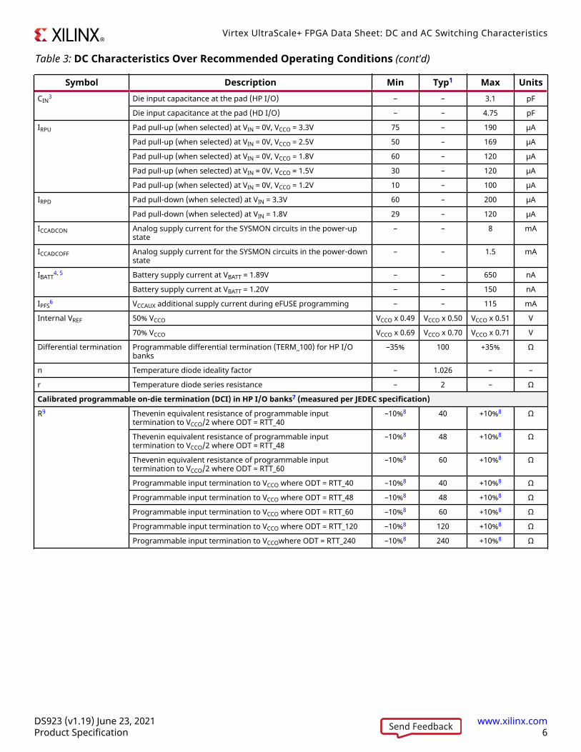
Table 3: DC Characteristics Over Recommended Operating Conditions (cont'd)
Symbol Description Min Typ1 Max UnitsCIN3 Die input capacitance at the pad (HP I/O) – – 3.1 pF
Die input capacitance at the pad (HD I/O) – – 4.75 pF
IRPU Pad pull-up (when selected) at VIN = 0V, VCCO = 3.3V 75 – 190 µA
Pad pull-up (when selected) at VIN = 0V, VCCO = 2.5V 50 – 169 µA
Pad pull-up (when selected) at VIN = 0V, VCCO = 1.8V 60 – 120 µA
Pad pull-up (when selected) at VIN = 0V, VCCO = 1.5V 30 – 120 µA
Pad pull-up (when selected) at VIN = 0V, VCCO = 1.2V 10 – 100 µA
IRPD Pad pull-down (when selected) at VIN = 3.3V 60 – 200 µA
Pad pull-down (when selected) at VIN = 1.8V 29 – 120 µA
ICCADCON Analog supply current for the SYSMON circuits in the power-upstate
– – 8 mA
ICCADCOFF Analog supply current for the SYSMON circuits in the power-downstate
– – 1.5 mA
IBATT4, 5 Battery supply current at VBATT = 1.89V – – 650 nA
Battery supply current at VBATT = 1.20V – – 150 nA
IPFS6 VCCAUX additional supply current during eFUSE programming – – 115 mA
Internal VREF 50% VCCO VCCO x 0.49 VCCO x 0.50 VCCO x 0.51 V
70% VCCO VCCO x 0.69 VCCO x 0.70 VCCO x 0.71 V
Differential termination Programmable differential termination (TERM_100) for HP I/Obanks
–35% 100 +35% Ω
n Temperature diode ideality factor – 1.026 – –
r Temperature diode series resistance – 2 – Ω
Calibrated programmable on-die termination (DCI) in HP I/O banks7 (measured per JEDEC specification)
R9 Thevenin equivalent resistance of programmable inputtermination to VCCO/2 where ODT = RTT_40
–10%8 40 +10%8 Ω
Thevenin equivalent resistance of programmable inputtermination to VCCO/2 where ODT = RTT_48
–10%8 48 +10%8 Ω
Thevenin equivalent resistance of programmable inputtermination to VCCO/2 where ODT = RTT_60
–10%8 60 +10%8 Ω
Programmable input termination to VCCO where ODT = RTT_40 –10%8 40 +10%8 Ω
Programmable input termination to VCCO where ODT = RTT_48 –10%8 48 +10%8 Ω
Programmable input termination to VCCO where ODT = RTT_60 –10%8 60 +10%8 Ω
Programmable input termination to VCCO where ODT = RTT_120 –10%8 120 +10%8 Ω
Programmable input termination to VCCOwhere ODT = RTT_240 –10%8 240 +10%8 Ω
Virtex UltraScale+ FPGA Data Sheet: DC and AC Switching Characteristics
DS923 (v1.19) June 23, 2021 www.xilinx.comProduct Specification 6Send Feedback

Table 3: DC Characteristics Over Recommended Operating Conditions (cont'd)
Symbol Description Min Typ1 Max UnitsUncalibrated programmable on-die termination in HP I/Os banks (measured per JEDEC specification)
R9 Thevenin equivalent resistance of programmable inputtermination to VCCO/2 where ODT = RTT_40
–50% 40 +50% Ω
Thevenin equivalent resistance of programmable inputtermination to VCCO/2 where ODT = RTT_48
–50% 48 +50% Ω
Thevenin equivalent resistance of programmable inputtermination to VCCO/2 where ODT = RTT_60
–50% 60 +50% Ω
Programmable input termination to VCCO where ODT = RTT_40 –50% 40 +50% Ω
Programmable input termination to VCCO where ODT = RTT_48 –50% 48 +50% Ω
Programmable input termination to VCCO where ODT = RTT_60 –50% 60 +50% Ω
Programmable input termination to VCCO where ODT = RTT_120 –50% 120 +50% Ω
Programmable input termination to VCCO where ODT = RTT_240 –50% 240 +50% Ω
Uncalibrated programmable on-die termination in HD I/O banks (measured per JEDEC specification)
R9 Thevenin equivalent resistance of programmable inputtermination to VCCO/2 where ODT = RTT_48
–50% 48 +50% Ω
Notes:1. Typical values are specified at nominal voltage, 25°C.2. For the HP I/O banks with a VCCO of 1.8V and separated VCCO and VCCAUX_IO power supplies, the IL maximum current is 70 µA.3. This measurement represents the die capacitance at the pad, not including the package.4. Maximum value specified for worst case process at 25°C. For the XCVU5P, XCVU7P, XCVU9P, XCVU11P, XCVU13P, XCVU19P, XCVU27P,
XCVU29P, XCVU35P, XCVU37P, XCVU45P, XCVU47P, and XCVU57P devices, multiply the value by the number of super-logic regions (SLRs)in the device.
5. IBATT is measured when the battery-backed RAM (BBRAM) is enabled.6. Do not program eFUSE during device configuration (e.g., during configuration, during configuration readback, or when readback CRC is
active).7. VRP resistor tolerance is (240Ω ±1%).8. If VRP resides at a different bank (DCI cascade), the range increases to ±15%.9. On-die input termination resistance, for more information see the UltraScale Architecture SelectIO Resources User Guide (UG571).
Virtex UltraScale+ FPGA Data Sheet: DC and AC Switching Characteristics
DS923 (v1.19) June 23, 2021 www.xilinx.comProduct Specification 7Send Feedback

VIN Maximum Allowed AC Voltage Overshoot and UndershootTable 4: VIN Maximum Allowed AC Voltage Overshoot and Undershoot for HD I/O Banks
AC Voltage Overshoot1 % of UI2 at –40°C to 100°C AC Voltage Undershoot1 % of UI2 at –40°C to 100°CVCCO + 0.30 100% –0.30 100%
VCCO + 0.35 100% –0.35 90%
VCCO + 0.40 100% –0.40 78%
VCCO + 0.45 100% –0.45 40%
VCCO + 0.50 100% –0.50 24%
VCCO + 0.55 100% –0.55 18.0%
VCCO + 0.60 100% –0.60 13.0%
VCCO + 0.65 100% –0.65 10.8%
VCCO + 0.70 92% –0.70 9.0%
VCCO + 0.75 92% –0.75 7.0%
VCCO + 0.80 92% –0.80 6.0%
VCCO + 0.85 92% –0.85 5.0%
VCCO + 0.90 92% –0.90 4.0%
VCCO + 0.95 92% –0.95 2.5%
Notes:1. A total of 200 mA per bank should not be exceeded.2. For UI smaller than 20 µs.3. For the -1M devices, the temperature limits are –55°C to 125°C.
Table 5: VIN Maximum Allowed AC Voltage Overshoot and Undershoot for HP I/O Banks
AC Voltage Overshoot1 % of UI2 at –40°C to 100°C AC Voltage Undershoot1 % of UI2 at –40°C to 100°CVCCO + 0.30 100% –0.30 100%
VCCO + 0.35 100% –0.35 100%
VCCO + 0.40 92% –0.40 92%
VCCO + 0.45 50% –0.45 50%
VCCO + 0.50 20% –0.50 20%
VCCO + 0.55 10% –0.55 10%
VCCO + 0.60 6% –0.60 6%
VCCO + 0.65 2% –0.65 2%
VCCO + 0.70 2% –0.70 2%
Notes:1. A total of 200 mA per bank should not be exceeded.2. For UI smaller than 20 µs.3. For the -1M devices, the temperature limits are –55°C to 125°C.
Virtex UltraScale+ FPGA Data Sheet: DC and AC Switching Characteristics
DS923 (v1.19) June 23, 2021 www.xilinx.comProduct Specification 8Send Feedback

Quiescent Supply CurrentTable 6: Typical Quiescent Supply Current
Symbol Description1, 2, 3 DeviceSpeed Grade and VCCINT Operating Voltages
Units0.90V 0.85V 0.72V-3 -2 -1 -2
ICCINTQ Quiescent VCCINT supply current XCVU3P 2384 2276 2276 2017 mA
XCVU5P 4769 4552 4552 4034 mA
XCVU7P 4769 4552 4552 4034 mA
XCVU9P 7153 6828 6828 6050 mA
XCVU11P 7567 7202 7202 6332 mA
XCVU13P 10090 9602 9602 8442 mA
XCVU19P N/A 21219 21219 N/A mA
XCVU23P 6784 6480 6480 5758 mA
XCVU27P 9962 9516 9516 8449 mA
XCVU29P 9962 9516 9516 8449 mA
XCVU31P 2528 2406 2406 2115 mA
XCVU33P 2528 2406 2406 2115 mA
XCVU35P 5051 4807 4807 4226 mA
XCVU37P 7573 7207 7207 6336 mA
XCVU45P 5051 4807 4807 4226 mA
XCVU47P 7573 7207 7207 6336 mA
XCVU57P 9835 9421 9421 8425 mA
ICCINT_IOQ Quiescent VCCINT_IO supply current XCVU3P 149 144 144 144 mA
XCVU5P 298 287 287 287 mA
XCVU7P 298 287 287 287 mA
XCVU9P 447 431 431 431 mA
XCVU11P 182 176 176 176 mA
XCVU13P 243 234 234 234 mA
XCVU19P N/A 515 515 N/A mA
XCVU23P 234 226 226 226 mA
XCVU27P 241 232 232 232 mA
XCVU29P 241 232 232 232 mA
XCVU31P 747 723 723 723 mA
XCVU33P 747 723 723 723 mA
XCVU35P 776 750 750 750 mA
XCVU37P 804 778 778 778 mA
XCVU45P 776 750 750 750 mA
XCVU47P 804 778 778 778 mA
XCVU57P 946 915 915 915 mA
ICCOQ Quiescent VCCO supply current All devices 1 1 1 1 mA
Virtex UltraScale+ FPGA Data Sheet: DC and AC Switching Characteristics
DS923 (v1.19) June 23, 2021 www.xilinx.comProduct Specification 9Send Feedback
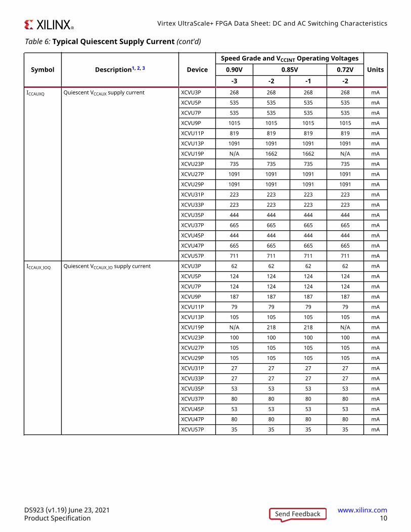
Table 6: Typical Quiescent Supply Current (cont'd)
Symbol Description1, 2, 3 DeviceSpeed Grade and VCCINT Operating Voltages
Units0.90V 0.85V 0.72V-3 -2 -1 -2
ICCAUXQ Quiescent VCCAUX supply current XCVU3P 268 268 268 268 mA
XCVU5P 535 535 535 535 mA
XCVU7P 535 535 535 535 mA
XCVU9P 1015 1015 1015 1015 mA
XCVU11P 819 819 819 819 mA
XCVU13P 1091 1091 1091 1091 mA
XCVU19P N/A 1662 1662 N/A mA
XCVU23P 735 735 735 735 mA
XCVU27P 1091 1091 1091 1091 mA
XCVU29P 1091 1091 1091 1091 mA
XCVU31P 223 223 223 223 mA
XCVU33P 223 223 223 223 mA
XCVU35P 444 444 444 444 mA
XCVU37P 665 665 665 665 mA
XCVU45P 444 444 444 444 mA
XCVU47P 665 665 665 665 mA
XCVU57P 711 711 711 711 mA
ICCAUX_IOQ Quiescent VCCAUX_IO supply current XCVU3P 62 62 62 62 mA
XCVU5P 124 124 124 124 mA
XCVU7P 124 124 124 124 mA
XCVU9P 187 187 187 187 mA
XCVU11P 79 79 79 79 mA
XCVU13P 105 105 105 105 mA
XCVU19P N/A 218 218 N/A mA
XCVU23P 100 100 100 100 mA
XCVU27P 105 105 105 105 mA
XCVU29P 105 105 105 105 mA
XCVU31P 27 27 27 27 mA
XCVU33P 27 27 27 27 mA
XCVU35P 53 53 53 53 mA
XCVU37P 80 80 80 80 mA
XCVU45P 53 53 53 53 mA
XCVU47P 80 80 80 80 mA
XCVU57P 35 35 35 35 mA
Virtex UltraScale+ FPGA Data Sheet: DC and AC Switching Characteristics
DS923 (v1.19) June 23, 2021 www.xilinx.comProduct Specification 10Send Feedback
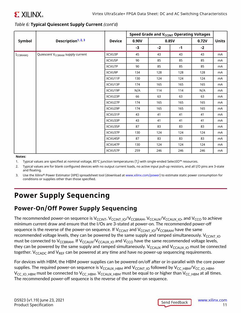
Table 6: Typical Quiescent Supply Current (cont'd)
Symbol Description1, 2, 3 DeviceSpeed Grade and VCCINT Operating Voltages
Units0.90V 0.85V 0.72V-3 -2 -1 -2
ICCBRAMQ Quiescent VCCBRAM supply current XCVU3P 45 43 43 43 mA
XCVU5P 90 85 85 85 mA
XCVU7P 90 85 85 85 mA
XCVU9P 134 128 128 128 mA
XCVU11P 130 124 124 124 mA
XCVU13P 174 165 165 165 mA
XCVU19P N/A 114 114 N/A mA
XCVU23P 66 63 63 63 mA
XCVU27P 174 165 165 165 mA
XCVU29P 174 165 165 165 mA
XCVU31P 43 41 41 41 mA
XCVU33P 43 41 41 41 mA
XCVU35P 87 83 83 83 mA
XCVU37P 130 124 124 124 mA
XCVU45P 87 83 83 83 mA
XCVU47P 130 124 124 124 mA
XCVU57P 259 246 246 246 mA
Notes:1. Typical values are specified at nominal voltage, 85°C junction temperatures (Tj) with single-ended SelectIO™ resources.2. Typical values are for blank configured devices with no output current loads, no active input pull-up resistors, and all I/O pins are 3-state
and floating.3. Use the Xilinx® Power Estimator (XPE) spreadsheet tool (download at www.xilinx.com/power) to estimate static power consumption for
conditions or supplies other than those specified.
Power Supply SequencingPower-On/Off Power Supply SequencingThe recommended power-on sequence is VCCINT, VCCINT_IO/VCCBRAM, VCCAUX/VCCAUX_IO, and VCCO to achieveminimum current draw and ensure that the I/Os are 3-stated at power-on. The recommended power-offsequence is the reverse of the power-on sequence. If VCCINT and VCCINT_IO/VCCBRAM have the samerecommended voltage levels, they can be powered by the same supply and ramped simultaneously. VCCINT_IOmust be connected to VCCBRAM. If VCCAUX/VCCAUX_IO and VCCO have the same recommended voltage levels,they can be powered by the same supply and ramped simultaneously. VCCAUX and VCCAUX_IO must be connectedtogether. VCCADC and VREF can be powered at any time and have no power-up sequencing requirements.
For devices with HBM, the HBM power supplies can be powered on/off after or in-parallel with the core powersupplies. The required power-on sequence is VCCAUX_HBM and VCCINT_IO followed by VCC_HBM/VCC_IO_HBM.VCC_IO_HBM must be connected to VCC_HBM. VCCAUX_HBM must be equal to or higher than VCC_HBM at all times.The recommended power-off sequence is the reverse of the power-on sequence.
Virtex UltraScale+ FPGA Data Sheet: DC and AC Switching Characteristics
DS923 (v1.19) June 23, 2021 www.xilinx.comProduct Specification 11Send Feedback

The recommended power-on sequence to achieve minimum current draw for the GTY or GTM transceivers isVCCINT, VCCINT_GT, VMGTAVCC, VMGTAVTT OR VMGTAVCC, VCCINT, VCCINT_GT, VMGTAVTT. There is no recommendedsequencing for VMGTVCCAUX. Both VMGTAVCC and VCCINT can be ramped simultaneously. When VCCINT andVCCINT_GT have the same recommended operating conditions, VCCINT and VCCINT_GT can be connected to thesame power regulation circuit. When VCCINT and VCCINT_GT are connected to separate regulation circuits,VCCINT_GT must be within the recommended operating condition before device configuration.The recommendedpower-off sequence is the reverse of the power-on sequence to achieve minimum current draw. If theserecommended sequences are not met, current drawn from VMGTAVTT can be higher than specifications duringpower-up and power-down.
Power Supply RequirementsTable 7 shows the minimum current, in addition to ICCQ maximum, required by each Virtex UltraScale+ FPGA forproper power-on and configuration. If these current minimums are met, the device powers on after all supplieshave passed through their power-on reset threshold voltages. The device must not be configured until afterVCCINT is applied. Once initialized and configured, use the Xilinx Power Estimator (XPE) tools to estimate currentdrain on these supplies. The XPE spreadsheet tool (download at https://www.xilinx.com/power) is also used toestimate power-on current for all supplies.
Table 7: Power-on Current by Device
Device ICCINTMIN ICCINT_IOMIN + ICCBRAMMIN ICCOMIN ICCAUXMIN + ICCAUX_IOMIN UnitsXCVU3P,XQVU3P
ICCINTQ + 2000 ICCBRAMQ + ICCINT_IOQ + 670 ICCOQ + 50 ICCAUXQ + ICCAUX_IOQ + 350 mA
XCVU5P ICCINTQ + 4000 ICCBRAMQ + ICCINT_IOQ + 1340 ICCOQ + 100 ICCAUXQ + ICCAUX_IOQ + 700 mA
XCVU7P,XQVU7P
ICCINTQ + 4000 ICCBRAMQ + ICCINT_IOQ + 1340 ICCOQ + 100 ICCAUXQ + ICCAUX_IOQ + 700 mA
XCVU9P ICCINTQ + 6000 ICCBRAMQ + ICCINT_IOQ + 2010 ICCOQ + 150 ICCAUXQ + ICCAUX_IOQ + 1050 mA
XCVU11P,XQVU11P
ICCINTQ + 6549 ICCBRAMQ + ICCINT_IOQ + 2194 ICCOQ + 164 ICCAUXQ + ICCAUX_IOQ + 1146 mA
XCVU13P ICCINTQ + 8731 ICCBRAMQ + ICCINT_IOQ + 2925 ICCOQ + 219 ICCAUXQ + ICCAUX_IOQ + 1528 mA
XCVU19P ICCINTQ + 20737 ICCBRAMQ + ICCINT_IOQ + 6947 ICCOQ + 519 ICCAUXQ + ICCAUX_IOQ + 3629 mA
XCVU23P ICCINTQ + 5225 ICCBRAMQ + ICCINT_IOQ + 1751 ICCOQ + 131 ICCAUXQ + ICCAUX_IOQ + 915 mA
XCVU27P ICCINTQ + 8770 ICCBRAMQ + ICCINT_IOQ + 2938 ICCOQ + 220 ICCAUXQ + ICCAUX_IOQ + 1535 mA
XCVU29P ICCINTQ + 8770 ICCBRAMQ + ICCINT_IOQ + 2938 ICCOQ + 220 ICCAUXQ + ICCAUX_IOQ + 1535 mA
XCVU31P ICCINTQ + 2232 ICCBRAMQ + ICCINT_IOQ + 2500 ICCOQ + 56 ICCAUXQ + ICCAUX_IOQ + 500 mA
XCVU33P ICCINTQ + 2232 ICCBRAMQ + ICCINT_IOQ + 2500 ICCOQ + 56 ICCAUXQ + ICCAUX_IOQ + 500 mA
XCVU35P ICCINTQ + 4424 ICCBRAMQ + ICCINT_IOQ + 3537 ICCOQ + 111 ICCAUXQ + ICCAUX_IOQ + 882 mA
XCVU37P ICCINTQ + 6617 ICCBRAMQ + ICCINT_IOQ + 4574 ICCOQ + 166 ICCAUXQ + ICCAUX_IOQ + 1264 mA
XCVU45P ICCINTQ + 4424 ICCBRAMQ + ICCINT_IOQ + 3537 ICCOQ + 111 ICCAUXQ + ICCAUX_IOQ + 882 mA
XCVU47P ICCINTQ + 6617 ICCBRAMQ + ICCINT_IOQ + 4574 ICCOQ + 166 ICCAUXQ + ICCAUX_IOQ + 1264 mA
XCVU57P ICCINTQ + 6617 ICCBRAMQ + ICCINT_IOQ + 4574 ICCOQ + 166 ICCAUXQ + ICCAUX_IOQ + 1264 mA
Virtex UltraScale+ FPGA Data Sheet: DC and AC Switching Characteristics
DS923 (v1.19) June 23, 2021 www.xilinx.comProduct Specification 12Send Feedback

Table 8: Power Supply Ramp Time
Symbol Description Min Max UnitsTVCCINT Ramp time from GND to 95% of VCCINT 0.2 40 ms
TVCCINT_IO Ramp time from GND to 95% of VCCINT_IO 0.2 40 ms
TVCCO Ramp time from GND to 95% of VCCO 0.2 40 ms
TVCCAUX Ramp time from GND to 95% of VCCAUX 0.2 40 ms
TVCCBRAM Ramp time from GND to 95% of VCCBRAM 0.2 40 ms
TVCC_HBM Ramp time from GND to 95% of VCC_HBM 0.2 40 ms
TVCC_IO_HBM Ramp time from GND to 95% of VCC_IO_HBM 0.2 40 ms
TVCCAUX_HBM Ramp time from GND to 95% of VCCAUX_HBM 0.2 40 ms
TMGTAVCC Ramp time from GND to 95% of VMGTAVCC 0.2 40 ms
TMGTAVTT Ramp time from GND to 95% of VMGTAVTT 0.2 40 ms
TMGTVCCAUX Ramp time from GND to 95% of VMGTVCCAUX 0.2 40 ms
DC Input and Output LevelsValues for VIL and VIH are recommended input voltages. Values for IOL and IOH are guaranteed over therecommended operating conditions at the VOL and VOH test points. Only selected standards are tested. Theseare chosen to ensure that all standards meet their specifications. The selected standards are tested at aminimum VCCO with the respective VOL and VOH voltage levels shown. Other standards are sample tested.
Virtex UltraScale+ FPGA Data Sheet: DC and AC Switching Characteristics
DS923 (v1.19) June 23, 2021 www.xilinx.comProduct Specification 13Send Feedback
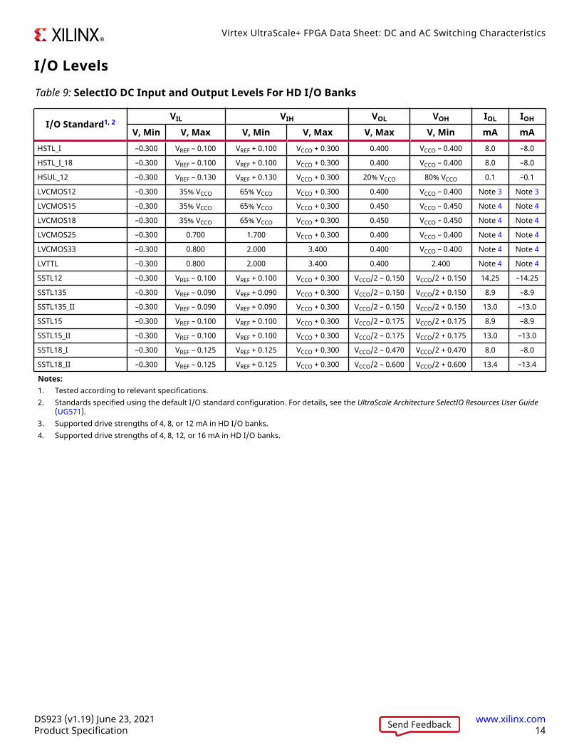
I/O LevelsTable 9: SelectIO DC Input and Output Levels For HD I/O Banks
I/O Standard1, 2VIL VIH VOL VOH IOL IOH
V, Min V, Max V, Min V, Max V, Max V, Min mA mAHSTL_I –0.300 VREF – 0.100 VREF + 0.100 VCCO + 0.300 0.400 VCCO – 0.400 8.0 –8.0
HSTL_I_18 –0.300 VREF – 0.100 VREF + 0.100 VCCO + 0.300 0.400 VCCO – 0.400 8.0 –8.0
HSUL_12 –0.300 VREF – 0.130 VREF + 0.130 VCCO + 0.300 20% VCCO 80% VCCO 0.1 –0.1
LVCMOS12 –0.300 35% VCCO 65% VCCO VCCO + 0.300 0.400 VCCO – 0.400 Note 3 Note 3
LVCMOS15 –0.300 35% VCCO 65% VCCO VCCO + 0.300 0.450 VCCO – 0.450 Note 4 Note 4
LVCMOS18 –0.300 35% VCCO 65% VCCO VCCO + 0.300 0.450 VCCO – 0.450 Note 4 Note 4
LVCMOS25 –0.300 0.700 1.700 VCCO + 0.300 0.400 VCCO – 0.400 Note 4 Note 4
LVCMOS33 –0.300 0.800 2.000 3.400 0.400 VCCO – 0.400 Note 4 Note 4
LVTTL –0.300 0.800 2.000 3.400 0.400 2.400 Note 4 Note 4
SSTL12 –0.300 VREF – 0.100 VREF + 0.100 VCCO + 0.300 VCCO/2 – 0.150 VCCO/2 + 0.150 14.25 –14.25
SSTL135 –0.300 VREF – 0.090 VREF + 0.090 VCCO + 0.300 VCCO/2 – 0.150 VCCO/2 + 0.150 8.9 –8.9
SSTL135_II –0.300 VREF – 0.090 VREF + 0.090 VCCO + 0.300 VCCO/2 – 0.150 VCCO/2 + 0.150 13.0 –13.0
SSTL15 –0.300 VREF – 0.100 VREF + 0.100 VCCO + 0.300 VCCO/2 – 0.175 VCCO/2 + 0.175 8.9 –8.9
SSTL15_II –0.300 VREF – 0.100 VREF + 0.100 VCCO + 0.300 VCCO/2 – 0.175 VCCO/2 + 0.175 13.0 –13.0
SSTL18_I –0.300 VREF – 0.125 VREF + 0.125 VCCO + 0.300 VCCO/2 – 0.470 VCCO/2 + 0.470 8.0 –8.0
SSTL18_II –0.300 VREF – 0.125 VREF + 0.125 VCCO + 0.300 VCCO/2 – 0.600 VCCO/2 + 0.600 13.4 –13.4
Notes:1. Tested according to relevant specifications.2. Standards specified using the default I/O standard configuration. For details, see the UltraScale Architecture SelectIO Resources User Guide
(UG571).3. Supported drive strengths of 4, 8, or 12 mA in HD I/O banks.4. Supported drive strengths of 4, 8, 12, or 16 mA in HD I/O banks.
Virtex UltraScale+ FPGA Data Sheet: DC and AC Switching Characteristics
DS923 (v1.19) June 23, 2021 www.xilinx.comProduct Specification 14Send Feedback
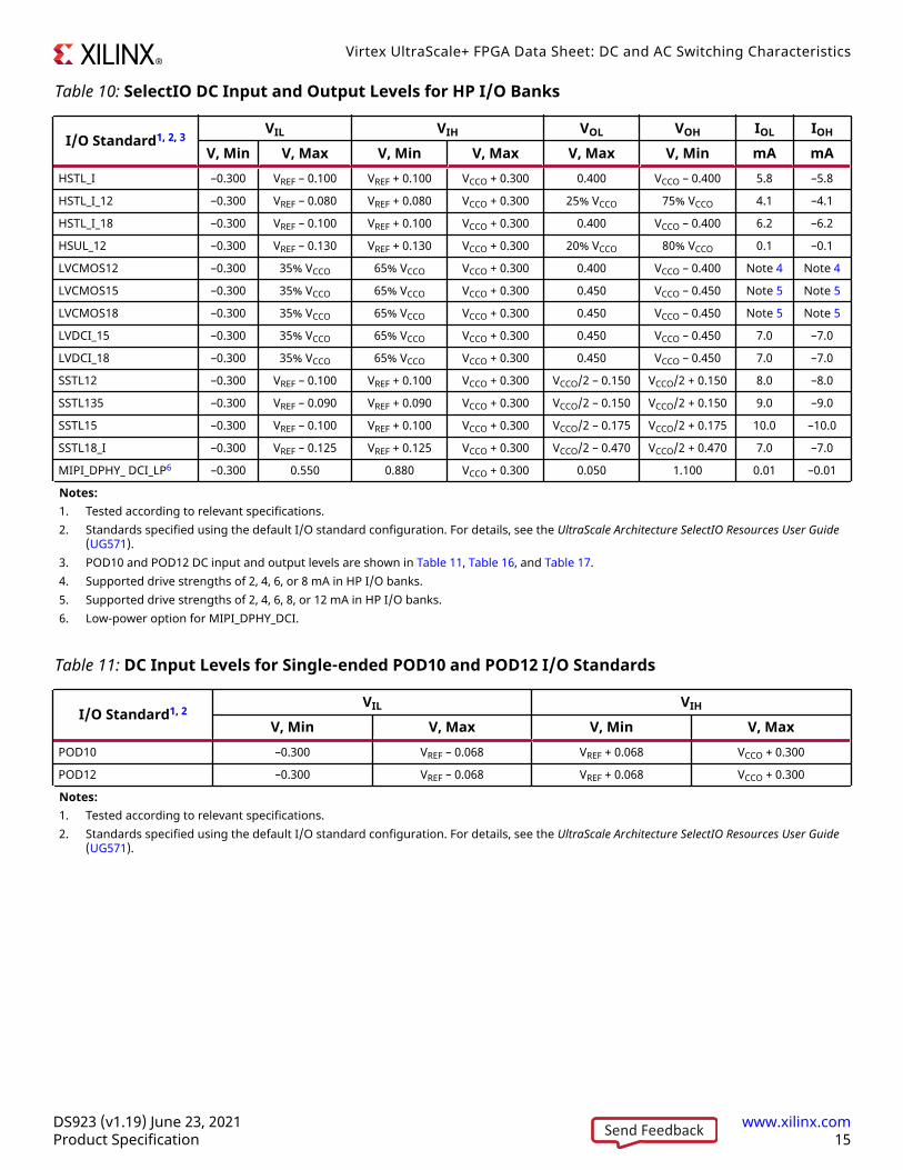
Table 10: SelectIO DC Input and Output Levels for HP I/O Banks
I/O Standard1, 2, 3VIL VIH VOL VOH IOL IOH
V, Min V, Max V, Min V, Max V, Max V, Min mA mAHSTL_I –0.300 VREF – 0.100 VREF + 0.100 VCCO + 0.300 0.400 VCCO – 0.400 5.8 –5.8
HSTL_I_12 –0.300 VREF – 0.080 VREF + 0.080 VCCO + 0.300 25% VCCO 75% VCCO 4.1 –4.1
HSTL_I_18 –0.300 VREF – 0.100 VREF + 0.100 VCCO + 0.300 0.400 VCCO – 0.400 6.2 –6.2
HSUL_12 –0.300 VREF – 0.130 VREF + 0.130 VCCO + 0.300 20% VCCO 80% VCCO 0.1 –0.1
LVCMOS12 –0.300 35% VCCO 65% VCCO VCCO + 0.300 0.400 VCCO – 0.400 Note 4 Note 4
LVCMOS15 –0.300 35% VCCO 65% VCCO VCCO + 0.300 0.450 VCCO – 0.450 Note 5 Note 5
LVCMOS18 –0.300 35% VCCO 65% VCCO VCCO + 0.300 0.450 VCCO – 0.450 Note 5 Note 5
LVDCI_15 –0.300 35% VCCO 65% VCCO VCCO + 0.300 0.450 VCCO – 0.450 7.0 –7.0
LVDCI_18 –0.300 35% VCCO 65% VCCO VCCO + 0.300 0.450 VCCO – 0.450 7.0 –7.0
SSTL12 –0.300 VREF – 0.100 VREF + 0.100 VCCO + 0.300 VCCO/2 – 0.150 VCCO/2 + 0.150 8.0 –8.0
SSTL135 –0.300 VREF – 0.090 VREF + 0.090 VCCO + 0.300 VCCO/2 – 0.150 VCCO/2 + 0.150 9.0 –9.0
SSTL15 –0.300 VREF – 0.100 VREF + 0.100 VCCO + 0.300 VCCO/2 – 0.175 VCCO/2 + 0.175 10.0 –10.0
SSTL18_I –0.300 VREF – 0.125 VREF + 0.125 VCCO + 0.300 VCCO/2 – 0.470 VCCO/2 + 0.470 7.0 –7.0
MIPI_DPHY_ DCI_LP6 –0.300 0.550 0.880 VCCO + 0.300 0.050 1.100 0.01 –0.01
Notes:1. Tested according to relevant specifications.2. Standards specified using the default I/O standard configuration. For details, see the UltraScale Architecture SelectIO Resources User Guide
(UG571).3. POD10 and POD12 DC input and output levels are shown in Table 11, Table 16, and Table 17.4. Supported drive strengths of 2, 4, 6, or 8 mA in HP I/O banks.5. Supported drive strengths of 2, 4, 6, 8, or 12 mA in HP I/O banks.6. Low-power option for MIPI_DPHY_DCI.
Table 11: DC Input Levels for Single-ended POD10 and POD12 I/O Standards
I/O Standard1, 2VIL VIH
V, Min V, Max V, Min V, MaxPOD10 –0.300 VREF – 0.068 VREF + 0.068 VCCO + 0.300
POD12 –0.300 VREF – 0.068 VREF + 0.068 VCCO + 0.300
Notes:1. Tested according to relevant specifications.2. Standards specified using the default I/O standard configuration. For details, see the UltraScale Architecture SelectIO Resources User Guide
(UG571).
Virtex UltraScale+ FPGA Data Sheet: DC and AC Switching Characteristics
DS923 (v1.19) June 23, 2021 www.xilinx.comProduct Specification 15Send Feedback
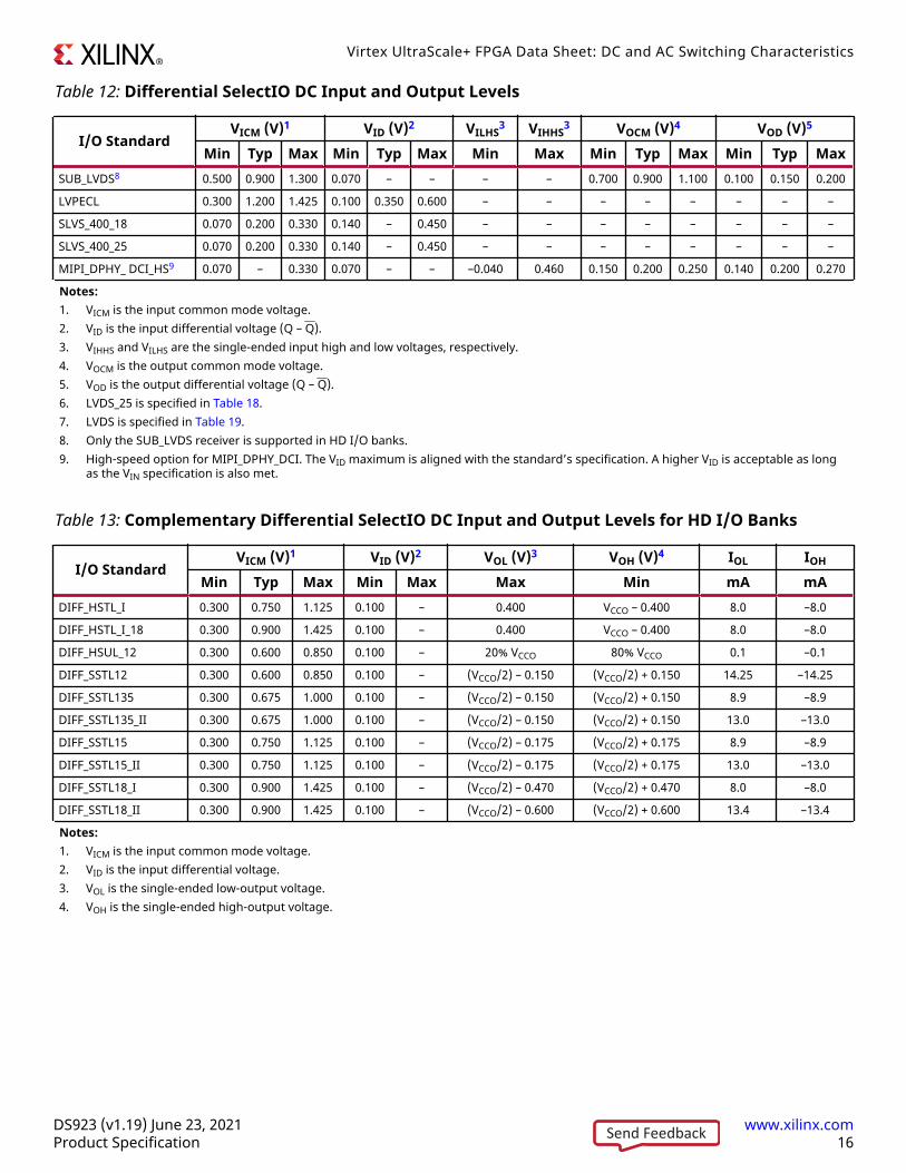
Table 12: Differential SelectIO DC Input and Output Levels
I/O StandardVICM (V)1 VID (V)2 VILHS3 VIHHS3 VOCM (V)4 VOD (V)5
Min Typ Max Min Typ Max Min Max Min Typ Max Min Typ MaxSUB_LVDS8 0.500 0.900 1.300 0.070 – – – – 0.700 0.900 1.100 0.100 0.150 0.200
LVPECL 0.300 1.200 1.425 0.100 0.350 0.600 – – – – – – – –
SLVS_400_18 0.070 0.200 0.330 0.140 – 0.450 – – – – – – – –
SLVS_400_25 0.070 0.200 0.330 0.140 – 0.450 – – – – – – – –
MIPI_DPHY_ DCI_HS9 0.070 – 0.330 0.070 – – –0.040 0.460 0.150 0.200 0.250 0.140 0.200 0.270
Notes:1. VICM is the input common mode voltage.2. VID is the input differential voltage (Q – Q).3. VIHHS and VILHS are the single-ended input high and low voltages, respectively.4. VOCM is the output common mode voltage.5. VOD is the output differential voltage (Q – Q).6. LVDS_25 is specified in Table 18.7. LVDS is specified in Table 19.8. Only the SUB_LVDS receiver is supported in HD I/O banks.9. High-speed option for MIPI_DPHY_DCI. The VID maximum is aligned with the standard’s specification. A higher VID is acceptable as long
as the VIN specification is also met.
Table 13: Complementary Differential SelectIO DC Input and Output Levels for HD I/O Banks
I/O StandardVICM (V)1 VID (V)2 VOL (V)3 VOH (V)4 IOL IOH
Min Typ Max Min Max Max Min mA mADIFF_HSTL_I 0.300 0.750 1.125 0.100 – 0.400 VCCO – 0.400 8.0 –8.0
DIFF_HSTL_I_18 0.300 0.900 1.425 0.100 – 0.400 VCCO – 0.400 8.0 –8.0
DIFF_HSUL_12 0.300 0.600 0.850 0.100 – 20% VCCO 80% VCCO 0.1 –0.1
DIFF_SSTL12 0.300 0.600 0.850 0.100 – (VCCO/2) – 0.150 (VCCO/2) + 0.150 14.25 –14.25
DIFF_SSTL135 0.300 0.675 1.000 0.100 – (VCCO/2) – 0.150 (VCCO/2) + 0.150 8.9 –8.9
DIFF_SSTL135_II 0.300 0.675 1.000 0.100 – (VCCO/2) – 0.150 (VCCO/2) + 0.150 13.0 –13.0
DIFF_SSTL15 0.300 0.750 1.125 0.100 – (VCCO/2) – 0.175 (VCCO/2) + 0.175 8.9 –8.9
DIFF_SSTL15_II 0.300 0.750 1.125 0.100 – (VCCO/2) – 0.175 (VCCO/2) + 0.175 13.0 –13.0
DIFF_SSTL18_I 0.300 0.900 1.425 0.100 – (VCCO/2) – 0.470 (VCCO/2) + 0.470 8.0 –8.0
DIFF_SSTL18_II 0.300 0.900 1.425 0.100 – (VCCO/2) – 0.600 (VCCO/2) + 0.600 13.4 –13.4
Notes:1. VICM is the input common mode voltage.2. VID is the input differential voltage.3. VOL is the single-ended low-output voltage.4. VOH is the single-ended high-output voltage.
Virtex UltraScale+ FPGA Data Sheet: DC and AC Switching Characteristics
DS923 (v1.19) June 23, 2021 www.xilinx.comProduct Specification 16Send Feedback

Table 14: Complementary Differential SelectIO DC Input and Output Levels for HP I/O Banks
I/O Standard1VICM (V)2 VID (V)3 VOL (V)4 VOH (V)5 IOL IOH
Min Typ Max Min Max Max Min mA mADIFF_HSTL_I 0.680 VCCO/2 (VCCO/2) + 0.150 0.100 – 0.400 VCCO – 0.400 5.8 –5.8
DIFF_HSTL_I_12 0.400 x VCCO VCCO/2 0.600 x VCCO 0.100 – 0.250 x VCCO 0.750 x VCCO 4.1 –4.1
DIFF_HSTL_I_18 (VCCO/2) – 0.175 VCCO/2 (VCCO/2) + 0.175 0.100 – 0.400 VCCO – 0.400 6.2 –6.2
DIFF_HSUL_12 (VCCO/2) – 0.120 VCCO/2 (VCCO/2) + 0.120 0.100 – 20% VCCO 80% VCCO 0.1 –0.1
DIFF_SSTL12 (VCCO/2) – 0.150 VCCO/2 (VCCO/2) + 0.150 0.100 – (VCCO/2) – 0.150 (VCCO/2) + 0.150 8.0 –8.0
DIFF_SSTL135 (VCCO/2) – 0.150 VCCO/2 (VCCO/2) + 0.150 0.100 – (VCCO/2) – 0.150 (VCCO/2) + 0.150 9.0 –9.0
DIFF_SSTL15 (VCCO/2) – 0.175 VCCO/2 (VCCO/2) + 0.175 0.100 – (VCCO/2) – 0.175 (VCCO/2) + 0.175 10.0 –10.0
DIFF_SSTL18_I (VCCO/2) – 0.175 VCCO/2 (VCCO/2) + 0.175 0.100 – (VCCO/2) – 0.470 (VCCO/2) + 0.470 7.0 –7.0
Notes:1. DIFF_POD10 and DIFF_POD12 HP I/O bank specifications are shown in Table 15, Table 16, Table 17.2. VICM is the input common mode voltage.3. VID is the input differential voltage.4. VOL is the single-ended low-output voltage.5. VOH is the single-ended high-output voltage.
Table 15: DC Input Levels for Differential POD10 and POD12 I/O Standards
I/O Standard1, 2VICM (V) VID (V)
Min Typ Max Min MaxDIFF_POD10 0.63 0.70 0.77 0.14 –
DIFF_POD12 0.76 0.84 0.92 0.16 –
Notes:1. Tested according to relevant specifications.2. Standards specified using the default I/O standard configuration. For details, see the UltraScale Architecture SelectIO Resources User Guide
(UG571).
Table 16: DC Output Levels for Single-ended and Differential POD10 and POD12 Standards
Symbol Description1, 2 VOUT Min Typ Max UnitsROL Pull-down resistance VOM_DC (as described in Table 17) 36 40 44 Ω
ROH Pull-up resistance VOM_DC (as described in Table 17) 36 40 44 Ω
Notes:1. Tested according to relevant specifications.2. Standards specified using the default I/O standard configuration. For details, see the UltraScale Architecture SelectIO Resources User Guide
(UG571).
Table 17: Definitions for DC Output Levels for Single-ended and Differential POD10 and POD12Standards
Symbol Description All Speed Grades UnitsVOM_DC DC output Mid measurement level (for IV curve linearity) 0.8 x VCCO V
Virtex UltraScale+ FPGA Data Sheet: DC and AC Switching Characteristics
DS923 (v1.19) June 23, 2021 www.xilinx.comProduct Specification 17Send Feedback

LVDS DC Specifications (LVDS_25)The LVDS_25 standard is available in the HD I/O banks. See the UltraScale Architecture SelectIO Resources UserGuide (UG571) for more information.
Table 18: LVDS_25 DC Specifications
Symbol DC Parameter Min Typ Max UnitsVCCO1 Supply voltage 2.375 2.500 2.625 V
VIDIFF Differential input voltage:(Q – Q), Q = High(Q – Q), Q = High
100 350 6002 mV
VICM Input common-mode voltage 0.300 1.200 1.425 V
Notes:1. LVDS_25 in HD I/O banks supports inputs only. LVDS_25 inputs without internal termination have no VCCO requirements. Any VCCO can be
chosen as long as the input voltage levels do not violate the Recommended Operating Condition (Table 2) specification for the VIN I/O pinvoltage.
2. Maximum VIDIFF value is specified for the maximum VICM specification. With a lower VICM, a higher VDIFF is tolerated only when therecommended operating conditions and overshoot/undershoot VIN specifications are maintained.
LVDS DC Specifications (LVDS)The LVDS standard is available in the HP I/O banks. See the UltraScale Architecture SelectIO Resources User Guide(UG571) for more information.
Table 19: LVDS DC Specifications
Symbol DC Parameter Conditions Min Typ Max UnitsVCCO1 Supply voltage 1.710 1.800 1.890 V
VODIFF2 Differential output voltage:(Q – Q), Q = High(Q – Q), Q = High
RT = 100Ω across Q and Q signals 247 350 454 mV
VOCM2 Output common-mode voltage RT = 100Ω across Q and Q signals 1.000 1.250 1.425 V
VIDIFF3 Differential input voltage:(Q – Q), Q = High(Q – Q), Q = High
100 350 6003 mV
VICM_DC4 Input common-mode voltage (DC coupling) 0.300 1.200 1.425 V
VICM_AC5 Input common-mode voltage (AC coupling) 0.600 – 1.100 V
Notes:1. In HP I/O banks, when LVDS is used with input-only functionality, it can be placed in a bank where the VCCO levels are different from the
specified level only if internal differential termination is not used. In this scenario, VCCO must be chosen to ensure the input pin voltagelevels do not violate the Recommended Operating Condition (Table 2) specification for the VIN I/O pin voltage.
2. VOCM and VODIFF values are for LVDS_PRE_EMPHASIS = FALSE.3. Maximum VIDIFF value is specified for the maximum VICM specification. With a lower VICM, a higher VDIFF is tolerated only when the
recommended operating conditions and overshoot/undershoot VIN specifications are maintained.4. Input common mode voltage for DC coupled configurations. EQUALIZATION = EQ_NONE (Default).5. External input common mode voltage specification for AC coupled configurations. EQUALIZATION = EQ_LEVEL0, EQ_LEVEL1, EQ_LEVEL2,
EQ_LEVEL3, EQ_LEVEL4.
Virtex UltraScale+ FPGA Data Sheet: DC and AC Switching Characteristics
DS923 (v1.19) June 23, 2021 www.xilinx.comProduct Specification 18Send Feedback

AC Switching CharacteristicsAll values represented in this data sheet are based on the speed specifications in the Vivado® Design Suite asoutlined in the following table.
Table 20: Speed Specification Version By Device
2021.1 Device1.27 XCVU3P, XCVU5P, XCVU7P, XCVU9P, XCVU11P, XCVU13P
XQVU3P, XQVU7P, XQVU11P
1.29 XCVU31P, XCVU33P, XCVU35P, XCVU37P, XCVU45P, XCVU47P
1.31 XCVU19P
1.33 XCVU23P
1.32 XCVU27P, XCVU29P
1.33 XCVU57P
Switching characteristics are specified on a per-speed-grade basis and can be designated as Advance,Preliminary, or Production. Each designation is defined as follows:
• Advance Product Specification: These specifications are based on simulations only and are typically availablesoon after device design specifications are frozen. Although speed grades with this designation areconsidered relatively stable and conservative, some under-reporting might still occur.
• Preliminary Product Specification: These specifications are based on complete ES (engineering sample)silicon characterization. Devices and speed grades with this designation are intended to give a betterindication of the expected performance of production silicon. The probability of under-reporting delays isgreatly reduced as compared to Advance data.
• Product Specification: These specifications are released once enough production silicon of a particulardevice family member has been characterized to provide full correlation between specifications and devicesover numerous production lots. There is no under-reporting of delays, and customers receive formalnotification of any subsequent changes. Typically, the slowest speed grades transition to production beforefaster speed grades.
Testing of AC Switching CharacteristicsInternal timing parameters are derived from measuring internal test patterns. All AC switching characteristicsare representative of worst-case supply voltage and junction temperature conditions.
For more specific, more precise, and worst-case guaranteed data, use the values reported by the static timinganalyzer and back-annotate to the simulation net list. Unless otherwise noted, values apply to all VirtexUltraScale+ FPGAs.
Speed Grade DesignationsBecause individual family members are produced at different times, the migration from one category to anotherdepends completely on the status of the fabrication process for each device. Table 21 correlates the currentstatus of the Virtex UltraScale+ FPGA on a per speed grade basis.
Virtex UltraScale+ FPGA Data Sheet: DC and AC Switching Characteristics
DS923 (v1.19) June 23, 2021 www.xilinx.comProduct Specification 19Send Feedback
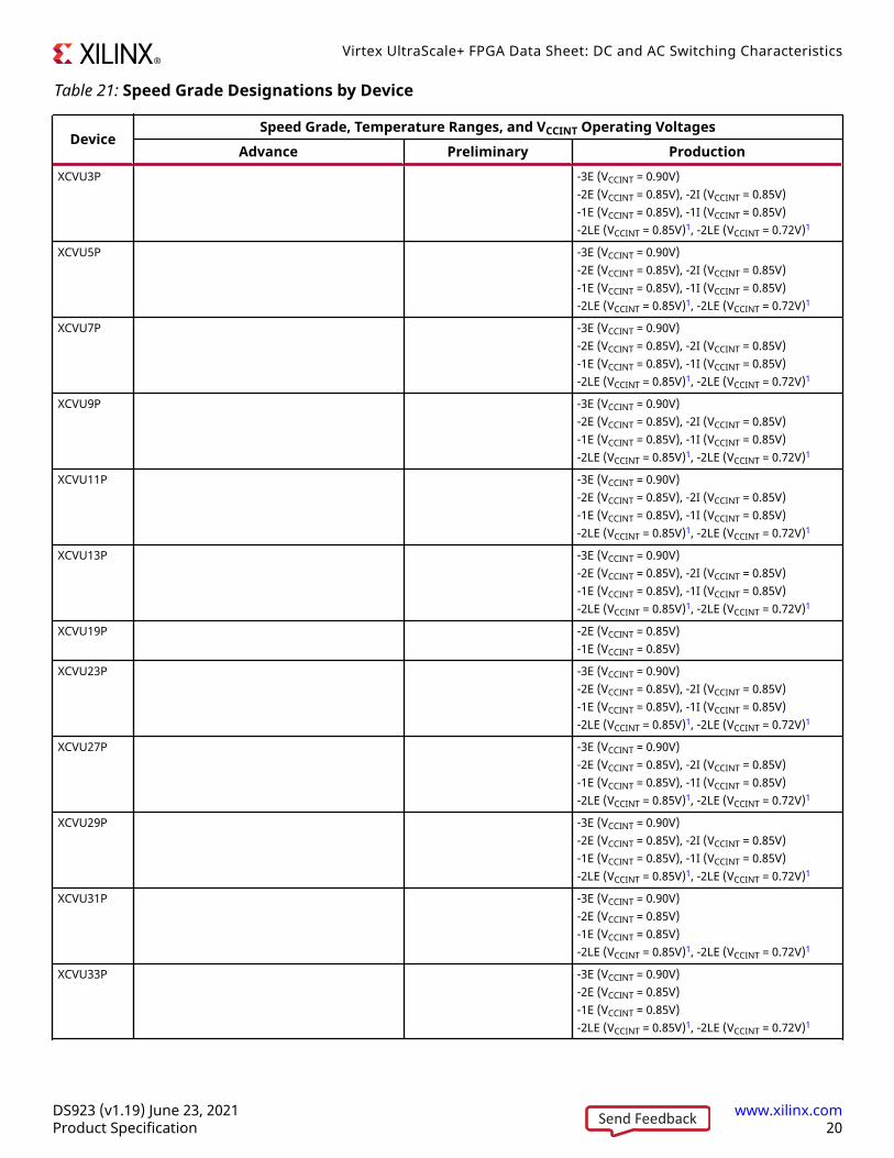
Table 21: Speed Grade Designations by Device
DeviceSpeed Grade, Temperature Ranges, and VCCINT Operating Voltages
Advance Preliminary ProductionXCVU3P -3E (VCCINT = 0.90V)
-2E (VCCINT = 0.85V), -2I (VCCINT = 0.85V)-1E (VCCINT = 0.85V), -1I (VCCINT = 0.85V)-2LE (VCCINT = 0.85V)1, -2LE (VCCINT = 0.72V)1
XCVU5P -3E (VCCINT = 0.90V)-2E (VCCINT = 0.85V), -2I (VCCINT = 0.85V)-1E (VCCINT = 0.85V), -1I (VCCINT = 0.85V)-2LE (VCCINT = 0.85V)1, -2LE (VCCINT = 0.72V)1
XCVU7P -3E (VCCINT = 0.90V)-2E (VCCINT = 0.85V), -2I (VCCINT = 0.85V)-1E (VCCINT = 0.85V), -1I (VCCINT = 0.85V)-2LE (VCCINT = 0.85V)1, -2LE (VCCINT = 0.72V)1
XCVU9P -3E (VCCINT = 0.90V)-2E (VCCINT = 0.85V), -2I (VCCINT = 0.85V)-1E (VCCINT = 0.85V), -1I (VCCINT = 0.85V)-2LE (VCCINT = 0.85V)1, -2LE (VCCINT = 0.72V)1
XCVU11P -3E (VCCINT = 0.90V)-2E (VCCINT = 0.85V), -2I (VCCINT = 0.85V)-1E (VCCINT = 0.85V), -1I (VCCINT = 0.85V)-2LE (VCCINT = 0.85V)1, -2LE (VCCINT = 0.72V)1
XCVU13P -3E (VCCINT = 0.90V)-2E (VCCINT = 0.85V), -2I (VCCINT = 0.85V)-1E (VCCINT = 0.85V), -1I (VCCINT = 0.85V)-2LE (VCCINT = 0.85V)1, -2LE (VCCINT = 0.72V)1
XCVU19P -2E (VCCINT = 0.85V)-1E (VCCINT = 0.85V)
XCVU23P -3E (VCCINT = 0.90V)-2E (VCCINT = 0.85V), -2I (VCCINT = 0.85V)-1E (VCCINT = 0.85V), -1I (VCCINT = 0.85V)-2LE (VCCINT = 0.85V)1, -2LE (VCCINT = 0.72V)1
XCVU27P -3E (VCCINT = 0.90V)-2E (VCCINT = 0.85V), -2I (VCCINT = 0.85V)-1E (VCCINT = 0.85V), -1I (VCCINT = 0.85V)-2LE (VCCINT = 0.85V)1, -2LE (VCCINT = 0.72V)1
XCVU29P -3E (VCCINT = 0.90V)-2E (VCCINT = 0.85V), -2I (VCCINT = 0.85V)-1E (VCCINT = 0.85V), -1I (VCCINT = 0.85V)-2LE (VCCINT = 0.85V)1, -2LE (VCCINT = 0.72V)1
XCVU31P -3E (VCCINT = 0.90V)-2E (VCCINT = 0.85V)-1E (VCCINT = 0.85V)-2LE (VCCINT = 0.85V)1, -2LE (VCCINT = 0.72V)1
XCVU33P -3E (VCCINT = 0.90V)-2E (VCCINT = 0.85V)-1E (VCCINT = 0.85V)-2LE (VCCINT = 0.85V)1, -2LE (VCCINT = 0.72V)1
Virtex UltraScale+ FPGA Data Sheet: DC and AC Switching Characteristics
DS923 (v1.19) June 23, 2021 www.xilinx.comProduct Specification 20Send Feedback
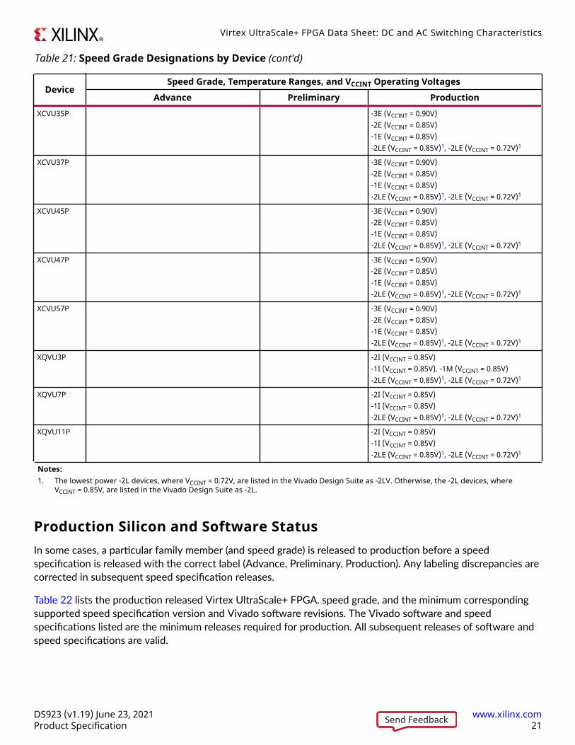
Table 21: Speed Grade Designations by Device (cont'd)
DeviceSpeed Grade, Temperature Ranges, and VCCINT Operating Voltages
Advance Preliminary ProductionXCVU35P -3E (VCCINT = 0.90V)
-2E (VCCINT = 0.85V)-1E (VCCINT = 0.85V)-2LE (VCCINT = 0.85V)1, -2LE (VCCINT = 0.72V)1
XCVU37P -3E (VCCINT = 0.90V)-2E (VCCINT = 0.85V)-1E (VCCINT = 0.85V)-2LE (VCCINT = 0.85V)1, -2LE (VCCINT = 0.72V)1
XCVU45P -3E (VCCINT = 0.90V)-2E (VCCINT = 0.85V)-1E (VCCINT = 0.85V)-2LE (VCCINT = 0.85V)1, -2LE (VCCINT = 0.72V)1
XCVU47P -3E (VCCINT = 0.90V)-2E (VCCINT = 0.85V)-1E (VCCINT = 0.85V)-2LE (VCCINT = 0.85V)1, -2LE (VCCINT = 0.72V)1
XCVU57P -3E (VCCINT = 0.90V)-2E (VCCINT = 0.85V)-1E (VCCINT = 0.85V)-2LE (VCCINT = 0.85V)1, -2LE (VCCINT = 0.72V)1
XQVU3P -2I (VCCINT = 0.85V)-1I (VCCINT = 0.85V), -1M (VCCINT = 0.85V)-2LE (VCCINT = 0.85V)1, -2LE (VCCINT = 0.72V)1
XQVU7P -2I (VCCINT = 0.85V)-1I (VCCINT = 0.85V)-2LE (VCCINT = 0.85V)1, -2LE (VCCINT = 0.72V)1
XQVU11P -2I (VCCINT = 0.85V)-1I (VCCINT = 0.85V)-2LE (VCCINT = 0.85V)1, -2LE (VCCINT = 0.72V)1
Notes:1. The lowest power -2L devices, where VCCINT = 0.72V, are listed in the Vivado Design Suite as -2LV. Otherwise, the -2L devices, where
VCCINT = 0.85V, are listed in the Vivado Design Suite as -2L.
Production Silicon and Software StatusIn some cases, a particular family member (and speed grade) is released to production before a speedspecification is released with the correct label (Advance, Preliminary, Production). Any labeling discrepancies arecorrected in subsequent speed specification releases.
Table 22 lists the production released Virtex UltraScale+ FPGA, speed grade, and the minimum correspondingsupported speed specification version and Vivado software revisions. The Vivado software and speedspecifications listed are the minimum releases required for production. All subsequent releases of software andspeed specifications are valid.
Virtex UltraScale+ FPGA Data Sheet: DC and AC Switching Characteristics
DS923 (v1.19) June 23, 2021 www.xilinx.comProduct Specification 21Send Feedback

Table 22: Virtex UltraScale+ FPGA Device Production Software and Speed Specification Release
DeviceSpeed Grade and VCCINT Operating Voltages
0.90V 0.85V 0.72V-3 -2 -1 -2L -2L
XCVU3P Vivado tools 2018.1 v1.19 Vivado tools 2017.1 v1.10 Vivado tools 2017.3.1 v1.16
XCVU5P Vivado tools 2018.1 v1.19 Vivado tools 2017.2 v1.12 Vivado tools 2017.3.1 v1.16
XCVU7P Vivado tools 2018.1 v1.19 Vivado tools 2017.2 v1.12 Vivado tools 2017.3.1 v1.16
XCVU9P Vivado tools 2018.1 v1.19 Vivado tools 2017.2 v1.12 Vivado tools 2017.3.1 v1.16
XCVU11P Vivado tools 2017.4.1 v1.18 Vivado tools 2017.2.1 v1.13 Vivado tools 2017.3.1 v1.16
XCVU13P Vivado tools 2017.4.1 v1.18 Vivado tools 2017.2.1 v1.13 Vivado tools 2017.3.1 v1.16
XCVU19P N/A Vivado tools 2020.2 v1.30 N/A N/A
XCVU23P Vivado tools 2020.2.2 v1.32 Vivado tools 2020.2.2 v1.32 Vivado tools 2020.2.2 v1.32
XCVU27P Vivado tools 2020.1.1 v1.30 Vivado tools 2019.1.3 v1.27 Vivado tools 2019.2 v1.28
XCVU29P Vivado tools 2020.1.1 v1.30 Vivado tools 2019.1.3 v1.27 Vivado tools 2019.2 v1.28
XCVU31P Vivado tools 2019.1 v1.25 Vivado tools 2018.3.1 v1.24 Vivado tools 2018.3.1 v1.24
XCVU33P Vivado tools 2019.1 v1.25 Vivado tools 2018.3.1 v1.24 Vivado tools 2018.3.1 v1.24
XCVU35P Vivado tools 2019.1 v1.25 Vivado tools 2018.3.1 v1.24 Vivado tools 2018.3.1 v1.24
XCVU37P Vivado tools 2019.1 v1.25 Vivado tools 2018.3.1 v1.24 Vivado tools 2018.3.1 v1.24
XCVU45P Vivado tools 2019.1 v1.25 Vivado tools 2019.1 v1.25 Vivado tools 2019.1 v1.25
XCVU47P Vivado tools 2019.1 v1.25 Vivado tools 2019.1 v1.25 Vivado tools 2019.1 v1.25
XCVU57P Vivado tools 2021.1 v1.33 Vivado tools 2021.1 v1.33 Vivado tools 2021.1 v1.33
XQVU3P N/A Vivado tools 2018.3 v1.23 Vivado tools 2018.3 v1.23
XQVU7P N/A Vivado tools 2018.3.1 v1.23 Vivado tools 2018.3.1 v1.23
XQVU11P N/A Vivado tools 2018.3.1 v1.23 Vivado tools 2018.3.1 v1.23
FPGA Logic Performance CharacteristicsThis section provides the performance characteristics of some common functions and designs implemented inthe Virtex UltraScale+ FPGAs. These values are subject to the same guidelines as the AC SwitchingCharacteristics section.
In each of the following LVDS performance tables, the I/O bank type is either high performance (HP) or highdensity (HD).
In LVDS component mode:
• For the input/output registers in HP I/O banks, the Vivado tools limit clock frequencies to 312.9 MHz for allspeed grades.
• For IDDR in HP I/O banks, Vivado tools limit clock frequencies to 625.0 MHz for all speed grades.• For ODDR in HP I/O banks, Vivado tools limit clock frequencies to 625.0 MHz for all speed grades.
Virtex UltraScale+ FPGA Data Sheet: DC and AC Switching Characteristics
DS923 (v1.19) June 23, 2021 www.xilinx.comProduct Specification 22Send Feedback

Table 23: LVDS Component Mode Performance
DescriptionI/O
BankType
Speed Grade and VCCINT Operating Voltages
Units0.90V 0.85V 0.72V
-3 -2 -1 -2Min Max Min Max Min Max Min Max
LVDS TX DDR (OSERDES 4:1, 8:1) HP 0 1250 0 1250 0 1250 0 1250 Mb/s
LVDS TX SDR (OSERDES 2:1, 4:1) HP 0 625 0 625 0 625 0 625 Mb/s
LVDS RX DDR (ISERDES 1:4, 1:8)1 HP 0 1250 0 1250 0 1250 0 1250 Mb/s
LVDS RX DDR HD 0 250 0 250 0 250 0 250 Mb/s
LVDS RX SDR (ISERDES 1:2, 1:4)1 HP 0 625 0 625 0 625 0 625 Mb/s
LVDS RX SDR HD 0 125 0 125 0 125 0 125 Mb/s
Notes:1. LVDS receivers are typically bounded with certain applications to achieve maximum performance. Package skews are not included and
should be removed through PCB routing.
Table 24: LVDS Native Mode Performance
Description1, 2 DATA_WIDTHI/O
BankType
Speed Grade and VCCINT Operating Voltages
Units0.90V 0.85V 0.72V
-3 -2 -1 -2Min Max Min Max Min Max Min Max
LVDS TX DDR(TX_BITSLICE)
4 HP 375 1600 375 1600 375 1600 375 1400 Mb/s
8 375 1600 375 1600 375 1600 375 1600 Mb/s
LVDS TX SDR(TX_BITSLICE)
4 HP 187.5 800 187.5 800 187.5 800 187.5 700 Mb/s
8 187.5 800 187.5 800 187.5 800 187.5 800 Mb/s
LVDS RX DDR(RX_BITSLICE)3
4 HP 375 16004 375 16004 375 16004 375 14004 Mb/s
8 375 16004 375 16004 375 16004 375 16004 Mb/s
LVDS RX SDR(RX_BITSLICE)3
4 HP 187.5 800 187.5 800 187.5 800 187.5 700 Mb/s
8 187.5 800 187.5 800 187.5 800 187.5 800 Mb/s
Notes:1. Native mode is supported through the High-Speed SelectIO Interface Wizard available with the Vivado Design Suite. The performance
values assume a source-synchronous interface.2. PLL settings can restrict the minimum allowable data rate. For example, when using the PLL with CLKOUTPHY_MODE = VCO_HALF the
minimum frequency is PLL_FVCOMIN/2.3. LVDS receivers are typically bounded with certain applications to achieve maximum performance. Package skews are not included and
should be removed through PCB routing.4. Asynchronous receiver performance is limited to 1300 Mb/s for -3/-2 speed grades and to 1250 Mb/s for -1 speed grades.
Virtex UltraScale+ FPGA Data Sheet: DC and AC Switching Characteristics
DS923 (v1.19) June 23, 2021 www.xilinx.comProduct Specification 23Send Feedback
Table 25: MIPI D-PHY Performance
DescriptionI/O
BankType
Speed Grade and VCCINT Operating VoltagesUnits0.90V 0.85V 0.72V
-3 -2 -1 -2MIPI D-PHY transmitter or receiver HP 1500 1500 1260 1260 Mb/s
Table 26: LVDS Native-Mode 1000BASE-X Support
Description1 I/O BankType
Speed Grade and VCCINT Operating Voltages0.90V 0.85V 0.72V
-3 -2 -1 -21000BASE-X HP Yes
Notes:1. 1000BASE-X support is based on the IEEE Standard for CSMA/CD Access Method and Physical Layer Specifications (IEEE Std 802.3-2008).
The following table provides the maximum data rates for applicable memory standards using the VirtexUltraScale+ FPGA memory PHY. Refer to Memory Interfaces for the complete list of memory interfacestandards supported and detailed specifications. The final performance of the memory interface is determinedthrough a complete design implemented in the Vivado Design Suite, following guidelines in the UltraScaleArchitecture PCB Design User Guide (UG583), electrical analysis, and characterization of the system.
Table 27: Maximum Physical Interface (PHY) Rate for Memory Interfaces
MemoryStandard DRAM Type
Speed Grade and VCCINT Operating VoltagesUnits0.90V 0.85V 0.72V
-3 -2 -1 -2DDR4 Single rank component 2666 2666 2400 2400 Mb/s
1 rank DIMM1, 2, 3 2400 2400 2133 2133 Mb/s
2 rank DIMM1, 4 2133 2133 1866 1866 Mb/s
4 rank DIMM1, 5 1600 1600 1333 1333 Mb/s
DDR3 Single rank component 2133 2133 2133 2133 Mb/s
1 rank DIMM1, 2 1866 1866 1866 1866 Mb/s
2 rank DIMM1, 4 1600 1600 1600 1600 Mb/s
4 rank DIMM1, 5 1066 1066 1066 1066 Mb/s
DDR3L Single rank component 1866 1866 1866 1866 Mb/s
1 rank DIMM1, 2 1600 1600 1600 1600 Mb/s
2 rank DIMM1, 4 1333 1333 1333 1333 Mb/s
4 rank DIMM1, 5 800 800 800 800 Mb/s
QDR II+ Single rank component6 633 633 600 600 MHz
RLDRAM 3 Single rank component 1200 1200 1066 1066 MHz
QDR IV XP Single rank component 1066 1066 1066 933 MHz
Virtex UltraScale+ FPGA Data Sheet: DC and AC Switching Characteristics
DS923 (v1.19) June 23, 2021 www.xilinx.comProduct Specification 24Send Feedback

Table 27: Maximum Physical Interface (PHY) Rate for Memory Interfaces (cont'd)
MemoryStandard DRAM Type
Speed Grade and VCCINT Operating VoltagesUnits0.90V 0.85V 0.72V
-3 -2 -1 -2LPDDR3 Single rank component 1600 1600 1600 1600 Mb/s
Notes:1. Dual in-line memory module (DIMM) includes RDIMM, SODIMM, UDIMM, and LRDIMM.2. Includes: 1 rank 1 slot, DDP 2 rank, LRDIMM 2 or 4 rank 1 slot.3. For the DDR4 DDP components at -3 and -2 (VCCINT = 0.85V) speed grades, the maximum data rate is 2133 Mb/s for six or more DDP
devices. For five or less DDP devices, use the single rank DIMM data rates for the -3 and -2 (VCCINT = 0.85V) speed grades.4. Includes: 2 rank 1 slot, 1 rank 2 slot, LRDIMM 2 rank 2 slot.5. Includes: 2 rank 2 slot, 4 rank 1 slot.6. The QDRII+ performance specifications are for burst-length 4 (BL = 4) implementations.
FPGA Logic Switching CharacteristicsThe following IOB high-density (HD) and IOB high-performance (HP) tables summarize the values of standard-specific data input delay adjustments, output delays terminating at pads (based on standard) and 3-state delays.
• TINBUF_DELAY_PAD_I is the delay from IOB pad through the input buffer to the I-pin of an IOB pad. The delayvaries depending on the capability of the SelectIO input buffer.
• TOUTBUF_DELAY_O_PAD is the delay from the O pin to the IOB pad through the output buffer of an IOB pad.The delay varies depending on the capability of the SelectIO output buffer.
• TOUTBUF_DELAY_TD_PAD is the delay from the T pin to the IOB pad through the output buffer of an IOB pad,when 3-state is disabled. The delay varies depending on the SelectIO capability of the output buffer. In HPI/O banks, the internal DCI termination turn-on time is always faster than TOUTBUF_DELAY_TD_PAD when theDCITERMDISABLE pin is used. In HD I/O banks, the on-die termination turn-on time is always faster thanTOUTBUF_DELAY_TD_PAD when the INTERMDISABLE pin is used.
IOB High Density (HD) Switching CharacteristicsTable 28: IOB High Density (HD) Switching Characteristics
I/O StandardsTINBUF_DELAY_PAD_I TOUTBUF_DELAY_O_PAD TOUTBUF_DELAY_TD_PAD
Units0.90V 0.85V 0.72V 0.90V 0.85V 0.72V 0.90V 0.85V 0.72V-3 -2 -1 -2 -3 -2 -1 -2 -3 -2 -1 -2
DIFF_HSTL_I_18_F 0.873 0.978 1.058 0.978 1.510 1.574 1.718 1.966 1.160 1.160 1.271 1.515 ns
DIFF_HSTL_I_18_S 0.873 0.978 1.058 0.978 1.742 1.805 1.950 2.197 1.748 1.748 1.867 2.103 ns
DIFF_HSTL_I_F 0.873 0.978 1.058 0.978 1.563 1.611 1.762 2.003 1.313 1.313 1.417 1.668 ns
DIFF_HSTL_I_S 0.873 0.978 1.058 0.978 1.696 1.798 1.913 2.190 1.630 1.630 1.780 1.985 ns
DIFF_HSUL_12_F 0.796 0.911 0.977 0.911 1.493 1.573 1.703 1.965 1.222 1.222 1.335 1.577 ns
DIFF_HSUL_12_S 0.796 0.911 0.977 0.911 1.653 1.711 1.864 2.103 1.536 1.536 1.665 1.891 ns
DIFF_SSTL12_F 0.796 0.906 0.977 0.906 1.577 1.643 1.792 2.035 1.285 1.285 1.423 1.640 ns
DIFF_SSTL12_S 0.796 0.906 0.977 0.906 1.726 1.784 1.948 2.176 1.567 1.567 1.706 1.922 ns
DIFF_SSTL135_F 0.807 0.927 0.995 0.927 1.558 1.625 1.765 2.017 1.341 1.341 1.458 1.696 ns
Virtex UltraScale+ FPGA Data Sheet: DC and AC Switching Characteristics
DS923 (v1.19) June 23, 2021 www.xilinx.comProduct Specification 25Send Feedback

Table 28: IOB High Density (HD) Switching Characteristics (cont'd)
I/O StandardsTINBUF_DELAY_PAD_I TOUTBUF_DELAY_O_PAD TOUTBUF_DELAY_TD_PAD
Units0.90V 0.85V 0.72V 0.90V 0.85V 0.72V 0.90V 0.85V 0.72V-3 -2 -1 -2 -3 -2 -1 -2 -3 -2 -1 -2
DIFF_SSTL135_II_F 0.807 0.927 0.995 0.927 1.560 1.623 1.770 2.015 1.325 1.325 1.470 1.680 ns
DIFF_SSTL135_II_S 0.807 0.927 0.995 0.927 1.694 1.768 1.916 2.160 1.722 1.722 1.911 2.077 ns
DIFF_SSTL135_S 0.807 0.927 0.995 0.927 1.796 1.869 2.025 2.261 1.814 1.814 1.976 2.169 ns
DIFF_SSTL15_F 0.840 0.928 1.020 0.928 1.559 1.628 1.771 2.020 1.374 1.374 1.483 1.729 ns
DIFF_SSTL15_II_F 0.840 0.928 1.020 0.928 1.574 1.622 1.778 2.014 1.356 1.356 1.442 1.711 ns
DIFF_SSTL15_II_S 0.840 0.928 1.020 0.928 1.769 1.821 1.987 2.213 1.895 1.895 2.047 2.250 ns
DIFF_SSTL15_S 0.840 0.928 1.020 0.928 1.752 1.824 1.977 2.216 1.743 1.743 1.907 2.098 ns
DIFF_SSTL18_II_F 0.873 0.961 1.038 0.961 1.672 1.729 1.880 2.121 1.377 1.377 1.492 1.732 ns
DIFF_SSTL18_II_S 0.873 0.961 1.038 0.961 1.748 1.796 1.965 2.188 1.616 1.616 1.800 1.971 ns
DIFF_SSTL18_I_F 0.873 0.961 1.038 0.961 1.539 1.609 1.755 2.001 1.220 1.220 1.313 1.575 ns
DIFF_SSTL18_I_S 0.873 0.961 1.038 0.961 1.728 1.786 1.942 2.178 1.677 1.677 1.836 2.032 ns
HSTL_I_18_F 0.854 0.947 1.021 0.947 1.510 1.574 1.718 1.966 1.160 1.160 1.271 1.515 ns
HSTL_I_18_S 0.854 0.947 1.021 0.947 1.742 1.805 1.950 2.197 1.748 1.748 1.867 2.103 ns
HSTL_I_F 0.748 0.856 0.900 0.856 1.563 1.611 1.762 2.003 1.313 1.313 1.417 1.668 ns
HSTL_I_S 0.748 0.856 0.900 0.856 1.696 1.798 1.913 2.190 1.630 1.630 1.780 1.985 ns
HSUL_12_F 0.712 0.780 0.867 0.780 1.493 1.573 1.703 1.965 1.222 1.222 1.335 1.577 ns
HSUL_12_S 0.712 0.780 0.867 0.780 1.653 1.711 1.864 2.103 1.536 1.536 1.665 1.891 ns
LVCMOS12_F_12 0.761 0.918 0.976 0.918 1.652 1.689 1.856 2.081 1.202 1.202 1.317 1.557 ns
LVCMOS12_F_4 0.761 0.918 0.976 0.918 1.714 1.742 1.922 2.134 1.353 1.353 1.478 1.708 ns
LVCMOS12_F_8 0.761 0.918 0.976 0.918 1.668 1.714 1.879 2.106 1.292 1.292 1.432 1.647 ns
LVCMOS12_S_12 0.761 0.918 0.976 0.918 2.019 2.073 2.247 2.465 1.581 1.581 1.717 1.936 ns
LVCMOS12_S_4 0.761 0.918 0.976 0.918 1.979 1.979 2.182 2.371 1.633 1.633 1.772 1.988 ns
LVCMOS12_S_8 0.761 0.918 0.976 0.918 2.132 2.205 2.406 2.597 1.767 1.767 1.928 2.122 ns
LVCMOS15_F_12 0.775 0.905 0.958 0.905 1.691 1.713 1.892 2.105 1.275 1.275 1.428 1.630 ns
LVCMOS15_F_16 0.775 0.905 0.958 0.905 1.665 1.722 1.881 2.114 1.260 1.260 1.407 1.615 ns
LVCMOS15_F_4 0.775 0.905 0.958 0.905 1.747 1.825 1.959 2.217 1.453 1.453 1.557 1.808 ns
LVCMOS15_F_8 0.775 0.905 0.958 0.905 1.721 1.778 1.930 2.170 1.378 1.378 1.458 1.733 ns
LVCMOS15_S_12 0.775 0.905 0.958 0.905 1.936 1.991 2.139 2.383 1.516 1.516 1.648 1.871 ns
LVCMOS15_S_16 0.775 0.905 0.958 0.905 2.172 2.172 2.389 2.564 1.707 1.707 1.888 2.062 ns
LVCMOS15_S_4 0.775 0.905 0.958 0.905 2.274 2.313 2.483 2.705 1.952 1.952 2.123 2.307 ns
LVCMOS15_S_8 0.775 0.905 0.958 0.905 2.170 2.170 2.400 2.562 1.817 1.817 1.984 2.172 ns
LVCMOS18_F_12 0.810 0.915 0.958 0.915 1.741 1.805 1.962 2.197 1.383 1.383 1.471 1.738 ns
LVCMOS18_F_16 0.810 0.915 0.958 0.915 1.698 1.785 1.917 2.177 1.338 1.338 1.446 1.693 ns
LVCMOS18_F_4 0.810 0.915 0.958 0.915 1.815 1.868 2.013 2.260 1.472 1.472 1.599 1.827 ns
LVCMOS18_F_8 0.810 0.915 0.958 0.915 1.785 1.797 1.979 2.189 1.384 1.384 1.487 1.739 ns
LVCMOS18_S_12 0.810 0.915 0.958 0.915 2.163 2.201 2.408 2.593 1.762 1.762 1.894 2.117 ns
LVCMOS18_S_16 0.810 0.915 0.958 0.915 2.102 2.173 2.362 2.565 1.702 1.702 1.834 2.057 ns
LVCMOS18_S_4 0.810 0.915 0.958 0.915 2.342 2.346 2.567 2.738 1.951 1.951 2.092 2.306 ns
LVCMOS18_S_8 0.810 0.915 0.958 0.915 2.275 2.292 2.511 2.684 1.848 1.848 2.008 2.203 ns
Virtex UltraScale+ FPGA Data Sheet: DC and AC Switching Characteristics
DS923 (v1.19) June 23, 2021 www.xilinx.comProduct Specification 26Send Feedback
Table 28: IOB High Density (HD) Switching Characteristics (cont'd)
I/O StandardsTINBUF_DELAY_PAD_I TOUTBUF_DELAY_O_PAD TOUTBUF_DELAY_TD_PAD
Units0.90V 0.85V 0.72V 0.90V 0.85V 0.72V 0.90V 0.85V 0.72V-3 -2 -1 -2 -3 -2 -1 -2 -3 -2 -1 -2
LVCMOS25_F_12 0.963 0.988 1.042 0.988 2.153 2.153 2.453 2.545 1.692 1.692 1.856 2.047 ns
LVCMOS25_F_16 0.963 0.988 1.042 0.988 2.105 2.105 2.406 2.497 1.623 1.623 1.786 1.978 ns
LVCMOS25_F_4 0.963 0.988 1.042 0.988 2.317 2.344 2.554 2.736 1.842 1.842 2.039 2.197 ns
LVCMOS25_F_8 0.963 0.988 1.042 0.988 2.184 2.184 2.516 2.576 1.726 1.726 1.910 2.081 ns
LVCMOS25_S_12 0.963 0.988 1.042 0.988 2.550 2.558 2.840 2.950 1.971 1.971 2.194 2.326 ns
LVCMOS25_S_16 0.963 0.988 1.042 0.988 2.449 2.449 2.740 2.841 1.852 1.852 2.063 2.207 ns
LVCMOS25_S_4 0.963 0.988 1.042 0.988 2.770 2.770 3.066 3.162 2.224 2.224 2.458 2.579 ns
LVCMOS25_S_8 0.963 0.988 1.042 0.988 2.663 2.663 2.963 3.055 2.091 2.091 2.373 2.446 ns
LVCMOS33_F_12 1.154 1.154 1.213 1.154 2.415 2.415 2.651 2.807 1.754 1.754 1.915 2.109 ns
LVCMOS33_F_16 1.154 1.154 1.213 1.154 2.381 2.383 2.603 2.775 1.734 1.734 1.869 2.089 ns
LVCMOS33_F_4 1.154 1.154 1.213 1.154 2.541 2.541 2.765 2.933 1.932 1.932 2.135 2.287 ns
LVCMOS33_F_8 1.154 1.154 1.213 1.154 2.603 2.603 2.822 2.995 1.937 1.937 2.130 2.292 ns
LVCMOS33_S_12 1.154 1.154 1.213 1.154 2.705 2.705 3.047 3.097 2.049 2.049 2.318 2.404 ns
LVCMOS33_S_16 1.154 1.154 1.213 1.154 2.714 2.714 3.024 3.106 2.028 2.028 2.232 2.383 ns
LVCMOS33_S_4 1.154 1.154 1.213 1.154 2.999 2.999 3.340 3.391 2.320 2.320 2.610 2.675 ns
LVCMOS33_S_8 1.154 1.154 1.213 1.154 2.929 2.929 3.260 3.321 2.260 2.260 2.532 2.615 ns
LVDS_25 0.980 1.003 1.116 1.003 N/A N/A N/A N/A N/A N/A N/A N/A ns
LVPECL 0.980 1.003 1.116 1.003 N/A N/A N/A N/A N/A N/A N/A N/A ns
LVTTL_F_12 1.164 1.164 1.223 1.164 2.415 2.415 2.651 2.807 1.754 1.754 1.915 2.109 ns
LVTTL_F_16 1.164 1.164 1.223 1.164 2.464 2.464 2.732 2.856 1.750 1.750 1.986 2.105 ns
LVTTL_F_4 1.164 1.164 1.223 1.164 2.541 2.541 2.765 2.933 1.932 1.932 2.135 2.287 ns
LVTTL_F_8 1.164 1.164 1.223 1.164 2.582 2.582 2.787 2.974 1.910 1.910 2.063 2.265 ns
LVTTL_S_12 1.164 1.164 1.223 1.164 2.731 2.731 3.075 3.123 2.072 2.072 2.343 2.427 ns
LVTTL_S_16 1.164 1.164 1.223 1.164 2.714 2.714 3.024 3.106 2.028 2.028 2.232 2.383 ns
LVTTL_S_4 1.164 1.164 1.223 1.164 2.999 2.999 3.340 3.391 2.320 2.320 2.610 2.675 ns
LVTTL_S_8 1.164 1.164 1.223 1.164 2.929 2.929 3.260 3.321 2.260 2.260 2.532 2.615 ns
SLVS_400_25 0.998 1.020 1.136 1.020 N/A N/A N/A N/A N/A N/A N/A N/A ns
SSTL12_F 0.712 0.780 0.867 0.780 1.577 1.643 1.792 2.035 1.285 1.285 1.423 1.640 ns
SSTL12_S 0.712 0.780 0.867 0.780 1.726 1.784 1.948 2.176 1.567 1.567 1.706 1.922 ns
SSTL135_F 0.731 0.798 0.881 0.798 1.558 1.625 1.765 2.017 1.341 1.341 1.458 1.696 ns
SSTL135_II_F 0.731 0.798 0.881 0.798 1.574 1.623 1.770 2.015 1.325 1.325 1.470 1.680 ns
SSTL135_II_S 0.731 0.798 0.881 0.798 1.694 1.768 1.916 2.160 1.722 1.722 1.911 2.077 ns
SSTL135_S 0.731 0.798 0.881 0.798 1.796 1.869 2.025 2.261 1.814 1.814 1.976 2.169 ns
SSTL15_F 0.731 0.838 0.880 0.838 1.544 1.612 1.754 2.004 1.357 1.357 1.464 1.712 ns
SSTL15_II_F 0.731 0.838 0.880 0.838 1.588 1.622 1.778 2.014 1.356 1.356 1.442 1.711 ns
SSTL15_II_S 0.731 0.838 0.880 0.838 1.769 1.821 1.987 2.213 1.895 1.895 2.047 2.250 ns
SSTL15_S 0.731 0.838 0.880 0.838 1.752 1.824 1.977 2.216 1.743 1.743 1.907 2.098 ns
SSTL18_II_F 0.854 0.947 1.021 0.947 1.699 1.729 1.880 2.121 1.377 1.377 1.492 1.732 ns
SSTL18_II_S 0.854 0.947 1.021 0.947 1.748 1.796 1.965 2.188 1.616 1.616 1.800 1.971 ns
Virtex UltraScale+ FPGA Data Sheet: DC and AC Switching Characteristics
DS923 (v1.19) June 23, 2021 www.xilinx.comProduct Specification 27Send Feedback

Table 28: IOB High Density (HD) Switching Characteristics (cont'd)
I/O StandardsTINBUF_DELAY_PAD_I TOUTBUF_DELAY_O_PAD TOUTBUF_DELAY_TD_PAD
Units0.90V 0.85V 0.72V 0.90V 0.85V 0.72V 0.90V 0.85V 0.72V-3 -2 -1 -2 -3 -2 -1 -2 -3 -2 -1 -2
SSTL18_I_F 0.854 0.947 1.021 0.947 1.566 1.609 1.755 2.001 1.220 1.220 1.313 1.575 ns
SSTL18_I_S 0.854 0.947 1.021 0.947 1.745 1.786 1.942 2.178 1.677 1.677 1.836 2.032 ns
SUB_LVDS 0.871 1.002 1.036 1.002 N/A N/A N/A N/A N/A N/A N/A N/A ns
IOB High Performance (HP) Switching CharacteristicsTable 29: IOB High Performance (HP) Switching Characteristics
I/O StandardsTINBUF_DELAY_PAD_I TOUTBUF_DELAY_O_PAD TOUTBUF_DELAY_TD_PAD
Units0.90V 0.85V 0.72V 0.90V 0.85V 0.72V 0.90V 0.85V 0.72V-3 -2 -1 -2 -3 -2 -1 -2 -3 -2 -1 -2
DIFF_HSTL_I_12_F 0.288 0.394 0.402 0.394 0.410 0.423 0.443 0.423 0.514 0.553 0.582 0.553 ns
DIFF_HSTL_I_12_M 0.288 0.394 0.402 0.394 0.552 0.552 0.583 0.552 0.632 0.641 0.679 0.641 ns
DIFF_HSTL_I_12_S 0.288 0.394 0.402 0.394 0.752 0.752 0.800 0.752 0.813 0.813 0.868 0.813 ns
DIFF_HSTL_I_18_F 0.259 0.319 0.339 0.319 0.439 0.456 0.474 0.456 0.549 0.576 0.606 0.576 ns
DIFF_HSTL_I_18_M 0.259 0.319 0.339 0.319 0.563 0.570 0.603 0.570 0.636 0.653 0.692 0.653 ns
DIFF_HSTL_I_18_S 0.259 0.319 0.339 0.319 0.782 0.782 0.834 0.782 0.816 0.816 0.871 0.816 ns
DIFF_HSTL_I_DCI_12_F 0.288 0.394 0.402 0.394 0.393 0.406 0.429 0.406 0.502 0.534 0.564 0.534 ns
DIFF_HSTL_I_DCI_12_M 0.288 0.394 0.402 0.394 0.546 0.557 0.587 0.557 0.636 0.653 0.694 0.653 ns
DIFF_HSTL_I_DCI_12_S 0.288 0.394 0.402 0.394 0.755 0.755 0.806 0.755 0.842 0.842 0.907 0.842 ns
DIFF_HSTL_I_DCI_18_F 0.259 0.323 0.339 0.323 0.422 0.445 0.461 0.445 0.509 0.566 0.595 0.566 ns
DIFF_HSTL_I_DCI_18_M 0.259 0.323 0.339 0.323 0.546 0.555 0.586 0.555 0.626 0.643 0.684 0.643 ns
DIFF_HSTL_I_DCI_18_S 0.259 0.323 0.339 0.323 0.762 0.762 0.818 0.762 0.836 0.836 0.900 0.836 ns
DIFF_HSTL_I_DCI_F 0.335 0.397 0.417 0.397 0.407 0.431 0.445 0.431 0.517 0.555 0.575 0.555 ns
DIFF_HSTL_I_DCI_M 0.335 0.397 0.417 0.397 0.549 0.553 0.583 0.553 0.634 0.644 0.684 0.644 ns
DIFF_HSTL_I_DCI_S 0.335 0.397 0.417 0.397 0.767 0.767 0.823 0.767 0.848 0.848 0.912 0.848 ns
DIFF_HSTL_I_F 0.304 0.404 0.417 0.404 0.409 0.423 0.443 0.423 0.514 0.549 0.581 0.549 ns
DIFF_HSTL_I_M 0.304 0.404 0.417 0.404 0.549 0.555 0.586 0.555 0.624 0.640 0.677 0.640 ns
DIFF_HSTL_I_S 0.304 0.404 0.417 0.404 0.767 0.767 0.818 0.767 0.811 0.811 0.866 0.811 ns
DIFF_HSUL_12_DCI_F 0.320 0.381 0.400 0.381 0.411 0.425 0.443 0.425 0.520 0.558 0.586 0.558 ns
DIFF_HSUL_12_DCI_M 0.320 0.381 0.400 0.381 0.546 0.557 0.587 0.557 0.636 0.653 0.694 0.653 ns
DIFF_HSUL_12_DCI_S 0.320 0.381 0.400 0.381 0.737 0.737 0.787 0.737 0.822 0.822 0.885 0.822 ns
DIFF_HSUL_12_F 0.322 0.394 0.402 0.394 0.394 0.412 0.430 0.412 0.494 0.538 0.566 0.538 ns
DIFF_HSUL_12_M 0.322 0.394 0.402 0.394 0.552 0.552 0.583 0.552 0.632 0.641 0.679 0.641 ns
DIFF_HSUL_12_S 0.322 0.394 0.402 0.394 0.752 0.752 0.800 0.752 0.813 0.813 0.868 0.813 ns
DIFF_POD10_DCI_F 0.289 0.411 0.430 0.411 0.407 0.425 0.444 0.425 0.512 0.555 0.584 0.555 ns
DIFF_POD10_DCI_M 0.289 0.411 0.430 0.411 0.533 0.542 0.571 0.542 0.618 0.640 0.681 0.640 ns
DIFF_POD10_DCI_S 0.289 0.411 0.430 0.411 0.754 0.754 0.815 0.754 0.850 0.850 0.917 0.850 ns
DIFF_POD10_F 0.288 0.411 0.433 0.411 0.425 0.438 0.459 0.438 0.531 0.569 0.601 0.569 ns
Virtex UltraScale+ FPGA Data Sheet: DC and AC Switching Characteristics
DS923 (v1.19) June 23, 2021 www.xilinx.comProduct Specification 28Send Feedback

Table 29: IOB High Performance (HP) Switching Characteristics (cont'd)
I/O StandardsTINBUF_DELAY_PAD_I TOUTBUF_DELAY_O_PAD TOUTBUF_DELAY_TD_PAD
Units0.90V 0.85V 0.72V 0.90V 0.85V 0.72V 0.90V 0.85V 0.72V-3 -2 -1 -2 -3 -2 -1 -2 -3 -2 -1 -2
DIFF_POD10_M 0.288 0.411 0.433 0.411 0.519 0.538 0.568 0.538 0.589 0.630 0.667 0.630 ns
DIFF_POD10_S 0.288 0.411 0.433 0.411 0.752 0.766 0.821 0.766 0.821 0.836 0.894 0.836 ns
DIFF_POD12_DCI_F 0.320 0.407 0.432 0.407 0.411 0.425 0.443 0.425 0.519 0.558 0.586 0.558 ns
DIFF_POD12_DCI_M 0.320 0.407 0.432 0.407 0.516 0.543 0.572 0.543 0.602 0.638 0.678 0.638 ns
DIFF_POD12_DCI_S 0.320 0.407 0.432 0.407 0.740 0.772 0.822 0.772 0.833 0.862 0.929 0.862 ns
DIFF_POD12_F 0.305 0.409 0.430 0.409 0.438 0.455 0.476 0.455 0.549 0.595 0.626 0.595 ns
DIFF_POD12_M 0.305 0.409 0.430 0.409 0.551 0.551 0.582 0.551 0.632 0.641 0.679 0.641 ns
DIFF_POD12_S 0.305 0.409 0.430 0.409 0.749 0.767 0.817 0.767 0.818 0.832 0.889 0.832 ns
DIFF_SSTL12_DCI_F 0.303 0.381 0.400 0.381 0.411 0.425 0.443 0.425 0.520 0.558 0.586 0.558 ns
DIFF_SSTL12_DCI_M 0.303 0.381 0.400 0.381 0.549 0.557 0.587 0.557 0.643 0.654 0.694 0.654 ns
DIFF_SSTL12_DCI_S 0.303 0.381 0.400 0.381 0.754 0.754 0.803 0.754 0.842 0.842 0.908 0.842 ns
DIFF_SSTL12_F 0.288 0.394 0.402 0.394 0.394 0.412 0.430 0.412 0.494 0.538 0.566 0.538 ns
DIFF_SSTL12_M 0.288 0.394 0.402 0.394 0.550 0.553 0.584 0.553 0.630 0.641 0.676 0.641 ns
DIFF_SSTL12_S 0.288 0.394 0.402 0.394 0.758 0.758 0.808 0.758 0.823 0.823 0.879 0.823 ns
DIFF_SSTL135_DCI_F 0.303 0.371 0.402 0.371 0.392 0.411 0.428 0.411 0.494 0.537 0.565 0.537 ns
DIFF_SSTL135_DCI_M 0.303 0.371 0.402 0.371 0.551 0.551 0.582 0.551 0.643 0.645 0.685 0.645 ns
DIFF_SSTL135_DCI_S 0.303 0.371 0.402 0.371 0.746 0.746 0.799 0.746 0.829 0.829 0.893 0.829 ns
DIFF_SSTL135_F 0.289 0.375 0.402 0.375 0.393 0.408 0.428 0.408 0.491 0.528 0.561 0.528 ns
DIFF_SSTL135_M 0.289 0.375 0.402 0.375 0.548 0.555 0.585 0.555 0.621 0.641 0.679 0.641 ns
DIFF_SSTL135_S 0.289 0.375 0.402 0.375 0.772 0.772 0.823 0.772 0.827 0.827 0.878 0.827 ns
DIFF_SSTL15_DCI_F 0.335 0.397 0.417 0.397 0.394 0.412 0.429 0.412 0.497 0.531 0.563 0.531 ns
DIFF_SSTL15_DCI_M 0.335 0.397 0.417 0.397 0.549 0.553 0.583 0.553 0.632 0.645 0.685 0.645 ns
DIFF_SSTL15_DCI_S 0.335 0.397 0.417 0.397 0.768 0.768 0.822 0.768 0.847 0.847 0.912 0.847 ns
DIFF_SSTL15_F 0.304 0.404 0.417 0.404 0.409 0.424 0.445 0.424 0.513 0.551 0.577 0.551 ns
DIFF_SSTL15_M 0.304 0.404 0.417 0.404 0.547 0.554 0.585 0.554 0.624 0.639 0.677 0.639 ns
DIFF_SSTL15_S 0.304 0.404 0.417 0.404 0.767 0.767 0.817 0.767 0.813 0.813 0.867 0.813 ns
DIFF_SSTL18_I_DCI_F 0.256 0.320 0.336 0.320 0.422 0.445 0.461 0.445 0.540 0.566 0.595 0.566 ns
DIFF_SSTL18_I_DCI_M 0.256 0.320 0.336 0.320 0.552 0.554 0.585 0.554 0.629 0.644 0.683 0.644 ns
DIFF_SSTL18_I_DCI_S 0.256 0.320 0.336 0.320 0.762 0.762 0.818 0.762 0.837 0.837 0.899 0.837 ns
DIFF_SSTL18_I_F 0.256 0.316 0.336 0.316 0.439 0.454 0.476 0.454 0.549 0.578 0.608 0.578 ns
DIFF_SSTL18_I_M 0.256 0.316 0.336 0.316 0.567 0.571 0.603 0.571 0.535 0.652 0.692 0.652 ns
DIFF_SSTL18_I_S 0.256 0.316 0.336 0.316 0.782 0.782 0.835 0.782 0.816 0.816 0.870 0.816 ns
HSLVDCI_15_F 0.336 0.393 0.415 0.393 0.407 0.425 0.443 0.425 0.513 0.548 0.579 0.548 ns
HSLVDCI_15_M 0.336 0.393 0.415 0.393 0.548 0.552 0.581 0.552 0.635 0.644 0.684 0.644 ns
HSLVDCI_15_S 0.336 0.393 0.415 0.393 0.748 0.748 0.802 0.748 0.827 0.827 0.890 0.827 ns
HSLVDCI_18_F 0.367 0.424 0.447 0.424 0.424 0.445 0.461 0.445 0.541 0.566 0.595 0.566 ns
HSLVDCI_18_M 0.367 0.424 0.447 0.424 0.563 0.567 0.598 0.567 0.647 0.658 0.699 0.658 ns
HSLVDCI_18_S 0.367 0.424 0.447 0.424 0.761 0.761 0.817 0.761 0.836 0.836 0.900 0.836 ns
HSTL_I_12_F 0.322 0.378 0.399 0.378 0.410 0.423 0.443 0.423 0.514 0.553 0.582 0.553 ns
Virtex UltraScale+ FPGA Data Sheet: DC and AC Switching Characteristics
DS923 (v1.19) June 23, 2021 www.xilinx.comProduct Specification 29Send Feedback
Table 29: IOB High Performance (HP) Switching Characteristics (cont'd)
I/O StandardsTINBUF_DELAY_PAD_I TOUTBUF_DELAY_O_PAD TOUTBUF_DELAY_TD_PAD
Units0.90V 0.85V 0.72V 0.90V 0.85V 0.72V 0.90V 0.85V 0.72V-3 -2 -1 -2 -3 -2 -1 -2 -3 -2 -1 -2
HSTL_I_12_M 0.322 0.378 0.399 0.378 0.551 0.551 0.582 0.551 0.632 0.642 0.679 0.642 ns
HSTL_I_12_S 0.322 0.378 0.399 0.378 0.750 0.750 0.799 0.750 0.813 0.813 0.868 0.813 ns
HSTL_I_18_F 0.258 0.322 0.339 0.322 0.439 0.456 0.474 0.456 0.549 0.576 0.606 0.576 ns
HSTL_I_18_M 0.258 0.322 0.339 0.322 0.562 0.569 0.602 0.569 0.637 0.653 0.692 0.653 ns
HSTL_I_18_S 0.258 0.322 0.339 0.322 0.781 0.781 0.833 0.781 0.816 0.816 0.871 0.816 ns
HSTL_I_DCI_12_F 0.322 0.378 0.399 0.378 0.393 0.406 0.429 0.406 0.502 0.534 0.564 0.534 ns
HSTL_I_DCI_12_M 0.322 0.378 0.399 0.378 0.551 0.556 0.586 0.556 0.644 0.654 0.694 0.654 ns
HSTL_I_DCI_12_S 0.322 0.378 0.399 0.378 0.754 0.754 0.803 0.754 0.842 0.842 0.907 0.842 ns
HSTL_I_DCI_18_F 0.258 0.321 0.339 0.321 0.422 0.445 0.461 0.445 0.509 0.566 0.595 0.566 ns
HSTL_I_DCI_18_M 0.258 0.321 0.339 0.321 0.551 0.554 0.585 0.554 0.634 0.643 0.684 0.643 ns
HSTL_I_DCI_18_S 0.258 0.321 0.339 0.321 0.761 0.761 0.817 0.761 0.836 0.836 0.900 0.836 ns
HSTL_I_DCI_F 0.288 0.393 0.415 0.393 0.407 0.431 0.445 0.431 0.517 0.555 0.575 0.555 ns
HSTL_I_DCI_M 0.288 0.393 0.415 0.393 0.548 0.552 0.581 0.552 0.635 0.644 0.684 0.644 ns
HSTL_I_DCI_S 0.288 0.393 0.415 0.393 0.766 0.766 0.821 0.766 0.847 0.847 0.912 0.847 ns
HSTL_I_F 0.322 0.378 0.399 0.378 0.409 0.423 0.443 0.423 0.514 0.549 0.581 0.549 ns
HSTL_I_M 0.322 0.378 0.399 0.378 0.548 0.554 0.585 0.554 0.624 0.640 0.677 0.640 ns
HSTL_I_S 0.322 0.378 0.399 0.378 0.766 0.766 0.816 0.766 0.811 0.811 0.866 0.811 ns
HSUL_12_DCI_F 0.319 0.378 0.399 0.378 0.411 0.425 0.443 0.425 0.520 0.558 0.586 0.558 ns
HSUL_12_DCI_M 0.319 0.378 0.399 0.378 0.551 0.556 0.586 0.556 0.644 0.654 0.694 0.654 ns
HSUL_12_DCI_S 0.319 0.378 0.399 0.378 0.736 0.736 0.784 0.736 0.821 0.821 0.886 0.821 ns
HSUL_12_F 0.305 0.378 0.399 0.378 0.394 0.412 0.430 0.412 0.494 0.538 0.566 0.538 ns
HSUL_12_M 0.305 0.378 0.399 0.378 0.551 0.551 0.582 0.551 0.632 0.642 0.679 0.642 ns
HSUL_12_S 0.305 0.378 0.399 0.378 0.750 0.750 0.799 0.750 0.813 0.813 0.868 0.813 ns
LVCMOS12_F_2 0.443 0.512 0.555 0.512 0.657 0.672 0.692 0.672 0.862 0.898 0.922 0.898 ns
LVCMOS12_F_4 0.443 0.512 0.555 0.512 0.486 0.504 0.521 0.504 0.645 0.664 0.693 0.664 ns
LVCMOS12_F_6 0.443 0.512 0.555 0.512 0.469 0.485 0.507 0.485 0.585 0.634 0.669 0.634 ns
LVCMOS12_F_8 0.443 0.512 0.555 0.512 0.457 0.465 0.489 0.465 0.592 0.611 0.666 0.611 ns
LVCMOS12_M_2 0.443 0.512 0.555 0.512 0.687 0.708 0.727 0.708 0.889 0.916 0.945 0.916 ns
LVCMOS12_M_4 0.443 0.512 0.555 0.512 0.533 0.550 0.573 0.550 0.629 0.664 0.690 0.664 ns
LVCMOS12_M_6 0.443 0.512 0.555 0.512 0.520 0.527 0.554 0.527 0.608 0.622 0.652 0.622 ns
LVCMOS12_M_8 0.443 0.512 0.555 0.512 0.532 0.540 0.571 0.540 0.606 0.614 0.649 0.614 ns
LVCMOS12_S_2 0.443 0.512 0.555 0.512 0.767 0.767 0.803 0.767 0.981 0.990 1.024 0.990 ns
LVCMOS12_S_4 0.443 0.512 0.555 0.512 0.666 0.666 0.704 0.666 0.803 0.803 0.848 0.803 ns
LVCMOS12_S_6 0.443 0.512 0.555 0.512 0.657 0.657 0.695 0.657 0.732 0.732 0.774 0.732 ns
LVCMOS12_S_8 0.443 0.512 0.555 0.512 0.708 0.708 0.761 0.708 0.745 0.745 0.790 0.745 ns
LVCMOS15_F_12 0.368 0.414 0.445 0.414 0.485 0.500 0.522 0.500 0.584 0.647 0.682 0.647 ns
LVCMOS15_F_2 0.368 0.414 0.445 0.414 0.686 0.702 0.722 0.702 0.893 0.919 0.940 0.919 ns
LVCMOS15_F_4 0.368 0.414 0.445 0.414 0.567 0.579 0.601 0.579 0.727 0.755 0.781 0.755 ns
LVCMOS15_F_6 0.368 0.414 0.445 0.414 0.533 0.547 0.569 0.547 0.684 0.711 0.742 0.711 ns
Virtex UltraScale+ FPGA Data Sheet: DC and AC Switching Characteristics
DS923 (v1.19) June 23, 2021 www.xilinx.comProduct Specification 30Send Feedback

Table 29: IOB High Performance (HP) Switching Characteristics (cont'd)
I/O StandardsTINBUF_DELAY_PAD_I TOUTBUF_DELAY_O_PAD TOUTBUF_DELAY_TD_PAD
Units0.90V 0.85V 0.72V 0.90V 0.85V 0.72V 0.90V 0.85V 0.72V-3 -2 -1 -2 -3 -2 -1 -2 -3 -2 -1 -2
LVCMOS15_F_8 0.368 0.414 0.445 0.414 0.500 0.518 0.538 0.518 0.635 0.686 0.703 0.686 ns
LVCMOS15_M_12 0.368 0.414 0.445 0.414 0.607 0.607 0.644 0.607 0.637 0.637 0.676 0.637 ns
LVCMOS15_M_2 0.368 0.414 0.445 0.414 0.736 0.741 0.770 0.741 0.929 0.938 0.962 0.938 ns
LVCMOS15_M_4 0.368 0.414 0.445 0.414 0.610 0.625 0.651 0.625 0.733 0.754 0.786 0.754 ns
LVCMOS15_M_6 0.368 0.414 0.445 0.414 0.564 0.576 0.604 0.576 0.655 0.674 0.710 0.674 ns
LVCMOS15_M_8 0.368 0.414 0.445 0.414 0.565 0.568 0.601 0.568 0.634 0.639 0.681 0.639 ns
LVCMOS15_S_12 0.368 0.414 0.445 0.414 0.788 0.788 0.855 0.788 0.695 0.695 0.733 0.695 ns
LVCMOS15_S_2 0.368 0.414 0.445 0.414 0.829 0.829 0.864 0.829 1.038 1.039 1.079 1.039 ns
LVCMOS15_S_4 0.368 0.414 0.445 0.414 0.687 0.687 0.725 0.687 0.813 0.813 0.851 0.813 ns
LVCMOS15_S_6 0.368 0.414 0.445 0.414 0.671 0.671 0.710 0.671 0.726 0.726 0.763 0.726 ns
LVCMOS15_S_8 0.368 0.414 0.445 0.414 0.704 0.704 0.755 0.704 0.721 0.721 0.758 0.721 ns
LVCMOS18_F_12 0.352 0.418 0.445 0.418 0.564 0.573 0.601 0.573 0.696 0.731 0.769 0.731 ns
LVCMOS18_F_2 0.352 0.418 0.445 0.418 0.723 0.739 0.760 0.739 0.918 0.945 0.971 0.945 ns
LVCMOS18_F_4 0.352 0.418 0.445 0.418 0.598 0.609 0.630 0.609 0.749 0.778 0.802 0.778 ns
LVCMOS18_F_6 0.352 0.418 0.445 0.418 0.598 0.603 0.633 0.603 0.781 0.781 0.808 0.781 ns
LVCMOS18_F_8 0.352 0.418 0.445 0.418 0.567 0.573 0.600 0.573 0.712 0.733 0.767 0.733 ns
LVCMOS18_M_12 0.352 0.418 0.445 0.418 0.640 0.640 0.678 0.640 0.670 0.670 0.709 0.670 ns
LVCMOS18_M_2 0.352 0.418 0.445 0.418 0.785 0.798 0.822 0.798 0.986 0.991 1.016 0.991 ns
LVCMOS18_M_4 0.352 0.418 0.445 0.418 0.658 0.664 0.693 0.664 0.786 0.798 0.836 0.798 ns
LVCMOS18_M_6 0.352 0.418 0.445 0.418 0.625 0.629 0.663 0.629 0.727 0.735 0.775 0.735 ns
LVCMOS18_M_8 0.352 0.418 0.445 0.418 0.626 0.626 0.661 0.626 0.705 0.705 0.746 0.705 ns
LVCMOS18_S_12 0.352 0.418 0.445 0.418 0.795 0.795 0.861 0.795 0.683 0.683 0.721 0.683 ns
LVCMOS18_S_2 0.352 0.418 0.445 0.418 0.861 0.862 0.897 0.862 1.061 1.076 1.098 1.076 ns
LVCMOS18_S_4 0.352 0.418 0.445 0.418 0.716 0.716 0.758 0.716 0.829 0.829 0.872 0.829 ns
LVCMOS18_S_6 0.352 0.418 0.445 0.418 0.682 0.682 0.724 0.682 0.724 0.724 0.762 0.724 ns
LVCMOS18_S_8 0.352 0.418 0.445 0.418 0.707 0.707 0.760 0.707 0.709 0.709 0.745 0.709 ns
LVDCI_15_F 0.369 0.425 0.462 0.425 0.407 0.426 0.443 0.426 0.514 0.548 0.581 0.548 ns
LVDCI_15_M 0.369 0.425 0.462 0.425 0.549 0.553 0.582 0.553 0.632 0.645 0.685 0.645 ns
LVDCI_15_S 0.369 0.425 0.462 0.425 0.749 0.749 0.803 0.749 0.821 0.821 0.890 0.821 ns
LVDCI_18_F 0.367 0.414 0.447 0.414 0.422 0.441 0.459 0.441 0.541 0.560 0.589 0.560 ns
LVDCI_18_M 0.367 0.414 0.447 0.414 0.546 0.554 0.585 0.554 0.622 0.644 0.683 0.644 ns
LVDCI_18_S 0.367 0.414 0.447 0.414 0.760 0.760 0.818 0.760 0.837 0.837 0.899 0.837 ns
LVDS 0.508 0.539 0.620 0.539 0.626 0.626 0.662 0.626 960.447 960.447 960.447 960.447 ns
MIPI_DPHY_DCI_HS 0.305 0.386 0.415 0.386 0.489 0.502 0.522 0.502 N/A N/A N/A N/A ns
MIPI_DPHY_DCI_LP 8.438 8.438 8.792 8.438 0.895 0.914 0.937 0.914 N/A N/A N/A N/A ns
POD10_DCI_F 0.336 0.408 0.430 0.408 0.407 0.425 0.444 0.425 0.512 0.555 0.584 0.555 ns
POD10_DCI_M 0.336 0.408 0.430 0.408 0.533 0.542 0.571 0.542 0.618 0.640 0.681 0.640 ns
POD10_DCI_S 0.336 0.408 0.430 0.408 0.724 0.754 0.815 0.754 0.815 0.850 0.917 0.850 ns
POD10_F 0.336 0.407 0.430 0.407 0.425 0.438 0.459 0.438 0.531 0.569 0.601 0.569 ns
Virtex UltraScale+ FPGA Data Sheet: DC and AC Switching Characteristics
DS923 (v1.19) June 23, 2021 www.xilinx.comProduct Specification 31Send Feedback
Table 29: IOB High Performance (HP) Switching Characteristics (cont'd)
I/O StandardsTINBUF_DELAY_PAD_I TOUTBUF_DELAY_O_PAD TOUTBUF_DELAY_TD_PAD
Units0.90V 0.85V 0.72V 0.90V 0.85V 0.72V 0.90V 0.85V 0.72V-3 -2 -1 -2 -3 -2 -1 -2 -3 -2 -1 -2
POD10_M 0.336 0.407 0.430 0.407 0.519 0.538 0.568 0.538 0.589 0.630 0.667 0.630 ns
POD10_S 0.336 0.407 0.430 0.407 0.752 0.766 0.821 0.766 0.821 0.836 0.894 0.836 ns
POD12_DCI_F 0.336 0.409 0.431 0.409 0.411 0.425 0.443 0.425 0.519 0.558 0.586 0.558 ns
POD12_DCI_M 0.336 0.409 0.431 0.409 0.516 0.543 0.572 0.543 0.602 0.638 0.678 0.638 ns
POD12_DCI_S 0.336 0.409 0.431 0.409 0.740 0.772 0.822 0.772 0.833 0.862 0.929 0.862 ns
POD12_F 0.336 0.409 0.431 0.409 0.438 0.455 0.476 0.455 0.549 0.595 0.626 0.595 ns
POD12_M 0.336 0.409 0.431 0.409 0.551 0.551 0.582 0.551 0.632 0.641 0.679 0.641 ns
POD12_S 0.336 0.409 0.431 0.409 0.749 0.767 0.817 0.767 0.818 0.832 0.889 0.832 ns
SLVS_400_18 0.492 0.539 0.620 0.539 N/A N/A N/A N/A N/A N/A N/A N/A ns
SSTL12_DCI_F 0.331 0.381 0.399 0.381 0.411 0.425 0.443 0.425 0.520 0.558 0.586 0.558 ns
SSTL12_DCI_M 0.331 0.381 0.399 0.381 0.549 0.557 0.587 0.557 0.643 0.654 0.694 0.654 ns
SSTL12_DCI_S 0.331 0.381 0.399 0.381 0.754 0.754 0.803 0.754 0.842 0.842 0.908 0.842 ns
SSTL12_F 0.320 0.403 0.403 0.403 0.394 0.412 0.430 0.412 0.494 0.538 0.566 0.538 ns
SSTL12_M 0.320 0.403 0.403 0.403 0.550 0.553 0.584 0.553 0.630 0.641 0.676 0.641 ns
SSTL12_S 0.320 0.403 0.403 0.403 0.758 0.758 0.808 0.758 0.823 0.823 0.879 0.823 ns
SSTL135_DCI_F 0.341 0.366 0.399 0.366 0.392 0.411 0.428 0.411 0.494 0.537 0.565 0.537 ns
SSTL135_DCI_M 0.341 0.366 0.399 0.366 0.551 0.551 0.582 0.551 0.643 0.645 0.685 0.645 ns
SSTL135_DCI_S 0.341 0.366 0.399 0.366 0.746 0.746 0.799 0.746 0.829 0.829 0.893 0.829 ns
SSTL135_F 0.321 0.378 0.399 0.378 0.393 0.408 0.428 0.408 0.491 0.528 0.561 0.528 ns
SSTL135_M 0.321 0.378 0.399 0.378 0.548 0.555 0.585 0.555 0.621 0.641 0.679 0.641 ns
SSTL135_S 0.321 0.378 0.399 0.378 0.772 0.772 0.823 0.772 0.827 0.827 0.878 0.827 ns
SSTL15_DCI_F 0.319 0.402 0.417 0.402 0.394 0.412 0.429 0.412 0.497 0.531 0.563 0.531 ns
SSTL15_DCI_M 0.319 0.402 0.417 0.402 0.549 0.553 0.583 0.553 0.632 0.645 0.685 0.645 ns
SSTL15_DCI_S 0.319 0.402 0.417 0.402 0.768 0.768 0.822 0.768 0.847 0.847 0.912 0.847 ns
SSTL15_F 0.320 0.371 0.400 0.371 0.393 0.408 0.428 0.408 0.494 0.530 0.556 0.530 ns
SSTL15_M 0.320 0.371 0.400 0.371 0.547 0.554 0.585 0.554 0.624 0.639 0.677 0.639 ns
SSTL15_S 0.320 0.371 0.400 0.371 0.767 0.767 0.817 0.767 0.813 0.813 0.867 0.813 ns
SSTL18_I_DCI_F 0.256 0.329 0.336 0.329 0.422 0.445 0.461 0.445 0.540 0.566 0.595 0.566 ns
SSTL18_I_DCI_M 0.256 0.329 0.336 0.329 0.552 0.554 0.585 0.554 0.629 0.644 0.683 0.644 ns
SSTL18_I_DCI_S 0.256 0.329 0.336 0.329 0.762 0.762 0.818 0.762 0.837 0.837 0.899 0.837 ns
SSTL18_I_F 0.259 0.316 0.337 0.316 0.439 0.454 0.476 0.454 0.549 0.578 0.608 0.578 ns
SSTL18_I_M 0.259 0.316 0.337 0.316 0.567 0.571 0.603 0.571 0.535 0.652 0.692 0.652 ns
SSTL18_I_S 0.259 0.316 0.337 0.316 0.782 0.782 0.835 0.782 0.816 0.816 0.870 0.816 ns
SUB_LVDS 0.508 0.539 0.620 0.539 0.658 0.660 0.692 0.660 907.387 969.863 969.863 969.863 ns
IOB 3-state Output Switching CharacteristicsTable 30 specifies the values of TOUTBUF_DELAY_TE_PAD and TINBUF_DELAY_IBUFDIS_O.
Virtex UltraScale+ FPGA Data Sheet: DC and AC Switching Characteristics
DS923 (v1.19) June 23, 2021 www.xilinx.comProduct Specification 32Send Feedback

• TOUTBUF_DELAY_TE_PAD is the delay from the T pin to the IOB pad through the output buffer of an IOB pad,when 3-state is enabled (i.e., a high impedance state).
• TINBUF_DELAY_IBUFDIS_O is the IOB delay from IBUFDISABLE to O output.
• In HP I/O banks, the internal DCI termination turn-off time is always faster than TOUTBUF_DELAY_TE_PAD whenthe DCITERMDISABLE pin is used.
• In HD I/O banks, the internal IN_TERM termination turn-off time is always faster than TOUTBUF_DELAY_TE_PADwhen the INTERMDISABLE pin is used.
Table 30: IOB 3-state Output Switching Characteristics
Symbol DescriptionSpeed Grade and VCCINT Operating Voltages
Units0.90V 0.85V 0.72V-3 -2 -1 -2
TOUTBUF_DELAY_TE_PAD T input to pad high-impedance for HDI/O banks
6.167 6.318 6.369 6.699 ns
T input to pad high-impedance for theHP I/O banks
5.330 5.330 5.341 5.330 ns
TINBUF_DELAY_IBUFDIS_O IBUF turn-on time from IBUFDISABLE toO output for HD I/O banks
2.266 2.266 2.430 2.266 ns
IBUF turn-on time from IBUFDISABLE toO output for the HP I/O banks
0.873 0.936 1.037 0.936 ns
Input Delay Measurement MethodologyThe following table shows the test setup parameters used for measuring input delay.
Table 31: Input Delay Measurement Methodology
Description I/O StandardAttribute VL1, 2 VH1, 2 VMEAS 1, 4 VREF 1, 3, 5
LVCMOS, 1.2V LVCMOS12 0.1 1.1 0.6 –
LVCMOS, LVDCI, HSLVDCI, 1.5V LVCMOS15, LVDCI_15,HSLVDCI_15
0.1 1.4 0.75 –
LVCMOS, LVDCI, HSLVDCI, 1.8V LVCMOS18, LVDCI_18,HSLVDCI_18
0.1 1.7 0.9 –
LVCMOS, 2.5V LVCMOS25 0.1 2.4 1.25 –
LVCMOS, 3.3V LVCMOS33 0.1 3.2 1.65 –
LVTTL, 3.3V LVTTL 0.1 3.2 1.65 –
HSTL (high-speed transceiver logic), class I, 1.2V HSTL_I_12 VREF – 0.25 VREF + 0.25 VREF 0.6
HSTL, class I, 1.5V HSTL_I VREF – 0.325 VREF + 0.325 VREF 0.75
HSTL, class I, 1.8V HSTL_I_18 VREF – 0.4 VREF + 0.4 VREF 0.9
HSUL (high-speed unterminated logic), 1.2V HSUL_12 VREF – 0.25 VREF + 0.25 VREF 0.6
SSTL12 (stub series terminated logic), 1.2V SSTL12 VREF – 0.25 VREF + 0.25 VREF 0.6
SSTL135 and SSTL135 class II, 1.35V SSTL135, SSTL135_II VREF – 0.2875 VREF + 0.2875 VREF 0.675
SSTL15 and SSTL15 class II, 1.5V SSTL15, SSTL15_II VREF – 0.325 VREF + 0.325 VREF 0.75
SSTL18, class I and II, 1.8V SSTL18_I, SSTL18_II VREF – 0.4 VREF + 0.4 VREF 0.9
POD10, 1.0V POD10 VREF – 0.2 VREF + 0.2 VREF 0.7
Virtex UltraScale+ FPGA Data Sheet: DC and AC Switching Characteristics
DS923 (v1.19) June 23, 2021 www.xilinx.comProduct Specification 33Send Feedback

Table 31: Input Delay Measurement Methodology (cont'd)
Description I/O StandardAttribute VL1, 2 VH1, 2 VMEAS 1, 4 VREF 1, 3, 5
POD12, 1.2V POD12 VREF – 0.24 VREF + 0.24 VREF 0.84
DIFF_HSTL, class I, 1.2V DIFF_HSTL_I_12 0.6 – 0.25 0.6 + 0.25 06 –
DIFF_HSTL, class I, 1.5V DIFF_HSTL_I 0.75 – 0.325 0.75 + 0.325 06 –
DIFF_HSTL, class I, 1.8V DIFF_HSTL_I_18 0.9 – 0.4 0.9 + 0.4 06 –
DIFF_HSUL, 1.2V DIFF_HSUL_12 0.6 – 0.25 0.6 + 0.25 06 –
DIFF_SSTL, 1.2V DIFF_SSTL12 0.6 – 0.25 0.6 + 0.25 06 –
DIFF_SSTL135 and DIFF_SSTL135 class II, 1.35V DIFF_SSTL135,DIFF_SSTL135_II
0.675 – 0.2875 0.675 + 0.2875 06 –
DIFF_SSTL15 and DIFF_SSTL15 class II, 1.5V DIFF_SSTL15,DIFF_SSTL15_II
0.75 – 0.325 0.75 + 0.325 06 –
DIFF_SSTL18_I, DIFF_SSTL18_II, 1.8V DIFF_SSTL18_I,DIFF_SSTL18_II
0.9 – 0.4 0.9 + 0.4 06 –
DIFF_POD10, 1.0V DIFF_POD10 0.5 – 0.2 0.5 + 0.2 06 –
DIFF_POD12, 1.2V DIFF_POD12 0.6 – 0.25 0.6 + 0.25 06 –
LVDS (low-voltage differential signaling), 1.8V LVDS 0.9 – 0.125 0.9 + 0.125 06 –
LVDS_25, 2.5V LVDS_25 1.25 – 0.125 1.25 + 0.125 06 –
SUB_LVDS, 1.8V SUB_LVDS 0.9 – 0.125 0.9 + 0.125 06 –
SLVS, 1.8V SLVS_400_18 0.9 – 0.125 0.9 + 0.125 06 –
SLVS, 2.5V SLVS_400_25 1.25 – 0.125 1.25 + 0.125 06 –
LVPECL, 2.5V LVPECL 1.25 – 0.125 1.25 + 0.125 06 –
MIPI D-PHY (high speed) 1.2V MIPI_DPHY_DCI_HS 0.2 – 0.125 0.2 + 0.125 06 –
MIPI D-PHY (low power) 1.2V MIPI_DPHY_DCI_LP 0.715 – 0.2 0.715 + 0.2 06 –
Notes:1. The input delay measurement methodology parameters for LVDCI/HSLVDCI are the same for LVCMOS standards of the same voltage.
Parameters for all other DCI standards are the same for the corresponding non-DCI standards.2. Input waveform switches between VL and VH.3. Measurements are made at typical, minimum, and maximum VREF values. Reported delays reflect worst case of these measurements.
VREF values listed are typical.4. Input voltage level from which measurement starts.5. This is an input voltage reference that bears no relation to the VREF/VMEAS parameters found in IBIS models and/or noted in Figure 1.6. The value given is the differential input voltage.
Output Delay Measurement MethodologyOutput delays are measured with short output traces. Standard termination was used for all testing. Thepropagation delay of the trace is characterized separately and subtracted from the final measurement, and istherefore not included in the generalized test setups shown in Figure 1 and Figure 2.
Virtex UltraScale+ FPGA Data Sheet: DC and AC Switching Characteristics
DS923 (v1.19) June 23, 2021 www.xilinx.comProduct Specification 34Send Feedback

Figure 1: Single-Ended Test Setup
VREF
RREF
VMEAS (voltage level when taking delay measurement)
CREF (probe capacitance)
Output
X16654-072117
Figure 2: Differential Test Setup
RREF VMEAS
+
–
CREF
Output
X16640-072117
Parameters VREF, RREF, CREF, and VMEAS fully describe the test conditions for each I/O standard. The mostaccurate prediction of propagation delay in any given application can be obtained through IBIS simulation, usingthis method:
1. Simulate the output driver of choice into the generalized test setup using values from Table 32.
2. Record the time to VMEAS.
3. Simulate the output driver of choice into the actual PCB trace and load using the appropriate IBIS model orcapacitance value to represent the load.
4. Record the time to VMEAS.
5. Compare the results of step 2 and step 4. The increase or decrease in delay yields the actual propagationdelay of the PCB trace.
Table 32: Output Delay Measurement Methodology
Description I/O Standard Attribute RREF(Ω)
CREF1
(pF)VMEAS
(V)VREF(V)
LVCMOS, 1.2V LVCMOS12 1M 0 0.6 0
LVCMOS, 1.5V LVCMOS15 1M 0 0.75 0
LVCMOS, 1.8V LVCMOS18 1M 0 0.9 0
LVCMOS, 2.5V LVCMOS25 1M 0 1.25 0
LVCMOS, 3.3V LVCMOS33 1M 0 1.65 0
LVTTL, 3.3V LVTTL 1M 0 1.65 0
LVDCI, HSLVDCI, 1.5V LVDCI_15, HSLVDCI_15 50 0 VREF 0.75
Virtex UltraScale+ FPGA Data Sheet: DC and AC Switching Characteristics
DS923 (v1.19) June 23, 2021 www.xilinx.comProduct Specification 35Send Feedback
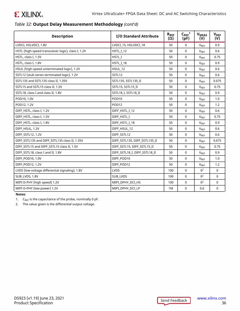
Table 32: Output Delay Measurement Methodology (cont'd)
Description I/O Standard Attribute RREF(Ω)
CREF1
(pF)VMEAS
(V)VREF(V)
LVDCI, HSLVDCI, 1.8V LVDCI_15, HSLVDCI_18 50 0 VREF 0.9
HSTL (high-speed transceiver logic), class I, 1.2V HSTL_I_12 50 0 VREF 0.6
HSTL, class I, 1.5V HSTL_I 50 0 VREF 0.75
HSTL, class I, 1.8V HSTL_I_18 50 0 VREF 0.9
HSUL (high-speed unterminated logic), 1.2V HSUL_12 50 0 VREF 0.6
SSTL12 (stub series terminated logic), 1.2V SSTL12 50 0 VREF 0.6
SSTL135 and SSTL135 class II, 1.35V SSTL135, SSTL135_II 50 0 VREF 0.675
SSTL15 and SSTL15 class II, 1.5V SSTL15, SSTL15_II 50 0 VREF 0.75
SSTL18, class I and class II, 1.8V SSTL18_I, SSTL18_II 50 0 VREF 0.9
POD10, 1.0V POD10 50 0 VREF 1.0
POD12, 1.2V POD12 50 0 VREF 1.2
DIFF_HSTL, class I, 1.2V DIFF_HSTL_I_12 50 0 VREF 0.6
DIFF_HSTL, class I, 1.5V DIFF_HSTL_I 50 0 VREF 0.75
DIFF_HSTL, class I, 1.8V DIFF_HSTL_I_18 50 0 VREF 0.9
DIFF_HSUL, 1.2V DIFF_HSUL_12 50 0 VREF 0.6
DIFF_SSTL12, 1.2V DIFF_SSTL12 50 0 VREF 0.6
DIFF_SSTL135 and DIFF_SSTL135 class II, 1.35V DIFF_SSTL135, DIFF_SSTL135_II 50 0 VREF 0.675
DIFF_SSTL15 and DIFF_SSTL15 class II, 1.5V DIFF_SSTL15, DIFF_SSTL15_II 50 0 VREF 0.75
DIFF_SSTL18, class I and II, 1.8V DIFF_SSTL18_I, DIFF_SSTL18_II 50 0 VREF 0.9
DIFF_POD10, 1.0V DIFF_POD10 50 0 VREF 1.0
DIFF_POD12, 1.2V DIFF_POD12 50 0 VREF 1.2
LVDS (low-voltage differential signaling), 1.8V LVDS 100 0 02 0
SUB_LVDS, 1.8V SUB_LVDS 100 0 02 0
MIPI D-PHY (high speed) 1.2V MIPI_DPHY_DCI_HS 100 0 02 0
MIPI D-PHY (low power) 1.2V MIPI_DPHY_DCI_LP 1M 0 0.6 0
Notes:1. CREF is the capacitance of the probe, nominally 0 pF.2. The value given is the differential output voltage.
Virtex UltraScale+ FPGA Data Sheet: DC and AC Switching Characteristics
DS923 (v1.19) June 23, 2021 www.xilinx.comProduct Specification 36Send Feedback
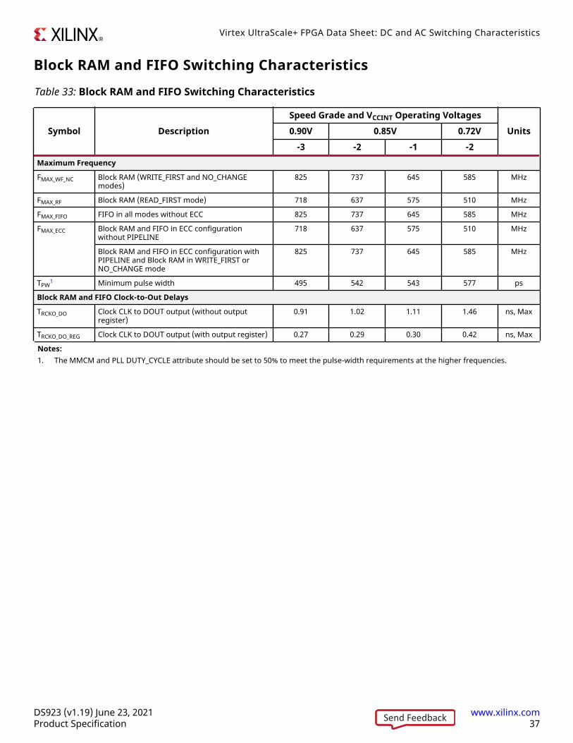
Block RAM and FIFO Switching CharacteristicsTable 33: Block RAM and FIFO Switching Characteristics
Symbol DescriptionSpeed Grade and VCCINT Operating Voltages
Units0.90V 0.85V 0.72V-3 -2 -1 -2
Maximum Frequency
FMAX_WF_NC Block RAM (WRITE_FIRST and NO_CHANGEmodes)
825 737 645 585 MHz
FMAX_RF Block RAM (READ_FIRST mode) 718 637 575 510 MHz
FMAX_FIFO FIFO in all modes without ECC 825 737 645 585 MHz
FMAX_ECC Block RAM and FIFO in ECC configurationwithout PIPELINE
718 637 575 510 MHz
Block RAM and FIFO in ECC configuration withPIPELINE and Block RAM in WRITE_FIRST orNO_CHANGE mode
825 737 645 585 MHz
TPW1 Minimum pulse width 495 542 543 577 ps
Block RAM and FIFO Clock-to-Out Delays
TRCKO_DO Clock CLK to DOUT output (without outputregister)
0.91 1.02 1.11 1.46 ns, Max
TRCKO_DO_REG Clock CLK to DOUT output (with output register) 0.27 0.29 0.30 0.42 ns, Max
Notes:1. The MMCM and PLL DUTY_CYCLE attribute should be set to 50% to meet the pulse-width requirements at the higher frequencies.
Virtex UltraScale+ FPGA Data Sheet: DC and AC Switching Characteristics
DS923 (v1.19) June 23, 2021 www.xilinx.comProduct Specification 37Send Feedback

UltraRAM Switching CharacteristicsThe UltraScale Architecture and Product Data Sheet: Overview (DS890) lists the Virtex UltraScale+ FPGAs thatinclude this memory.
Table 34: UltraRAM Switching Characteristics
Symbol DescriptionSpeed Grade and VCCINT Operating Voltages
Units0.90V 0.85V 0.72V-3 -2 -1 -2
Maximum Frequency
FMAX UltraRAM maximum frequency withOREG_B = True
650 600 575 500 MHz
FMAX_ECC_NOPIPELINE UltraRAM maximum frequency withOREG_B = False and EN_ECC_RD_B = True
435 400 386 312 MHz
FMAX_NOPIPELINE UltraRAM maximum frequency withOREG_B = False and EN_ECC_RD_B = False
528 500 478 404 MHz
TPW1 Minimum pulse width 650 700 730 800 ps
TRSTPW Asynchronous reset minimum pulse width. Onecycle required
1 clock cycle
Notes:1. The MMCM and PLL DUTY_CYCLE attribute should be set to 50% to meet the pulse-width requirements at the higher frequencies.
Input/Output Delay Switching CharacteristicsTable 35: Input/Output Delay Switching Characteristics
Symbol Description
Speed Grade and VCCINT OperatingVoltages
Units0.90V 0.85V 0.72V-3 -2 -1 -2
FREFCLK Reference clock frequency for IDELAYCTRL(component mode)
300 to 800 MHz
Reference clock frequency when usingBITSLICE_CONTROL with REFCLK (in native mode (forRX_BITSLICE only))
300 to 800 MHz
Reference clock frequency for BITSLICE_CONTROLwith PLL_CLK (in native mode)1
300 to2666.67
300 to2666.67
300 to 2400 300 to 2400 MHz
TMINPER_CLK Minimum period for IODELAY clock 3.195 3.195 3.195 3.195 ns
TMINPER_RST Minimum reset pulse width 52.00 ns
TIDELAY_RESOLUTION/TODELAY_RESOLUTION
IDELAY/ODELAY chain resolution 2.1 to 12 ps
Notes:1. PLL settings could restrict the minimum allowable data rate. For example, when using a PLL with CLKOUTPHY_MODE = VCO_HALF, the
minimum frequency is PLL_FVCOMIN/2.
Virtex UltraScale+ FPGA Data Sheet: DC and AC Switching Characteristics
DS923 (v1.19) June 23, 2021 www.xilinx.comProduct Specification 38Send Feedback

DSP48 Slice Switching CharacteristicsTable 36: DSP48 Slice Switching Characteristics
Symbol DescriptionSpeed Grade and VCCINT Operating Voltages
Units0.90V 0.85V 0.72V1
-3 -2 -1 -2Maximum Frequency
FMAX With all registers used 891 775 645 644 MHz
FMAX_PATDET With pattern detector 794 687 571 562 MHz
FMAX_MULT_NOMREG Two register multiply without MREG 635 544 456 440 MHz
FMAX_MULT_NOMREG_PATDET Two register multiply without MREGwith pattern detect
577 492 410 395 MHz
FMAX_PREADD_NOADREG Without ADREG 655 565 468 453 MHz
FMAX_NOPIPELINEREG Without pipeline registers (MREG,ADREG)
483 410 338 323 MHz
FMAX_NOPIPELINEREG_PATDET Without pipeline registers (MREG,ADREG) with pattern detect
448 379 314 299 MHz
Notes:1. For devices operating at the lower power VCCINT = 0.72V voltages, DSP cascades that cross the clock region center might operate below
the specified FMAX.
Clock Buffers and NetworksTable 37: Clock Buffers Switching Characteristics
Symbol DescriptionSpeed Grade and VCCINT Operating Voltages
Units0.90V 0.85V 0.72V-3 -2 -1 -2
Global Clock Switching Characteristics (Including BUFGCTRL)
FMAX Maximum frequency of a global clock tree (BUFG) 891 775 667 725 MHz
Global Clock Buffer with Input Divide Capability (BUFGCE_DIV)
FMAX Maximum frequency of a global clock buffer with inputdivide capability (BUFGCE_DIV)
891 775 667 725 MHz
Global Clock Buffer with Clock Enable (BUFGCE)
FMAX Maximum frequency of a global clock buffer with clockenable (BUFGCE)
891 775 667 725 MHz
Leaf Clock Buffer with Clock Enable (BUFCE_LEAF)
FMAX Maximum frequency of a leaf clock buffer with clockenable (BUFCE_LEAF)
891 775 667 725 MHz
GTY or GTM Clock Buffer with Clock Enable and Clock Input Divide Capability (BUFG_GT)
FMAX Maximum frequency of a serial transceiver clock bufferwith clock enable and clock input divide capability
512 512 512 512 MHz
Virtex UltraScale+ FPGA Data Sheet: DC and AC Switching Characteristics
DS923 (v1.19) June 23, 2021 www.xilinx.comProduct Specification 39Send Feedback

MMCM Switching CharacteristicsTable 38: MMCM Specification
Symbol DescriptionSpeed Grade and VCCINT Operating Voltages
Units0.90V 0.85V 0.72V-3 -2 -1 -2
MMCM_FINMAX Maximum input clock frequency 1066 933 800 933 MHz
MMCM_FINMIN Minimum input clock frequency 10 10 10 10 MHz
MMCM_FINJITTER Maximum input clock period jitter < 20% of clock input period or 1 ns Max
MMCM_FINDUTY Input duty cycle range: 10–49 MHz 25–75 %
Input duty cycle range: 50–199 MHz 30–70 %
Input duty cycle range: 200–399 MHz 35–65 %
Input duty cycle range: 400–499 MHz 40–60 %
Input duty cycle range: >500 MHz 45–55 %
MMCM_FMIN_PSCLK Minimum dynamic phase shift clockfrequency
0.01 0.01 0.01 0.01 MHz
MMCM_FMAX_PSCLK Maximum dynamic phase shift clockfrequency
550 500 450 500 MHz
MMCM_FVCOMIN Minimum MMCM VCO frequency 800 800 800 800 MHz
MMCM_FVCOMAX Maximum MMCM VCO frequency 1600 1600 1600 1600 MHz
MMCM_FBANDWIDTH Low MMCM bandwidth at typical1 1.00 1.00 1.00 1.00 MHz
High MMCM bandwidth at typical1 4.00 4.00 4.00 4.00 MHz
MMCM_TSTATPHAOFFSET Static phase offset of the MMCM outputs2 0.12 0.12 0.12 0.12 ns
MMCM_TOUTJITTER MMCM output jitter Note 3
MMCM_TOUTDUTY MMCM output clock duty cycle precision4 0.165 0.20 0.20 0.20 ns
MMCM_TLOCKMAX MMCM maximum lock time forMMCM_FPFDMIN
100 100 100 100 µs
MMCM_FOUTMAX MMCM maximum output frequency 891 775 667 725 MHz
MMCM_FOUTMIN MMCM minimum output frequency4, 5 6.25 6.25 6.25 6.25 MHz
MMCM_TEXTFDVAR External clock feedback variation < 20% of clock input period or 1 ns Max
MMCM_RSTMINPULSE Minimum reset pulse width 5.00 5.00 5.00 5.00 ns
MMCM_FPFDMAX Maximum frequency at the phasefrequency detector
550 500 450 500 MHz
MMCM_FPFDMIN Minimum frequency at the phasefrequency detector
10 10 10 10 MHz
MMCM_TFBDELAY Maximum delay in the feedback path 5 ns Max or one clock cycle
MMCM_FDPRCLK_MAX Maximum DRP clock frequency 250 250 250 250 MHz
Notes:1. The MMCM does not filter typical spread-spectrum input clocks because they are usually far below the bandwidth filter frequencies.2. The static offset is measured between any MMCM outputs with identical phase.3. Values for this parameter are available in the Clocking Wizard.4. Includes global clock buffer.5. Calculated as FVCO/128 assuming output duty cycle is 50%.
Virtex UltraScale+ FPGA Data Sheet: DC and AC Switching Characteristics
DS923 (v1.19) June 23, 2021 www.xilinx.comProduct Specification 40Send Feedback

PLL Switching CharacteristicsTable 39: PLL Specification
Symbol Description1
Speed Grade and VCCINT Operating VoltagesUnits0.90V 0.85V 0.72V
-3 -2 -1 -2PLL_FINMAX Maximum input clock frequency 1066 933 800 933 MHz
PLL_FINMIN Minimum input clock frequency 70 70 70 70 MHz
PLL_FINJITTER Maximum input clock period jitter < 20% of clock input period or 1 ns Max
PLL_FINDUTY Input duty cycle range: 70–399 MHz 35–65 %
Input duty cycle range: 400–499 MHz 40–60 %
Input duty cycle range: >500 MHz 45–55 %
PLL_FVCOMIN Minimum PLL VCO frequency 750 750 750 750 MHz
PLL_FVCOMAX Maximum PLL VCO frequency 1500 1500 1500 1500 MHz
PLL_TSTATPHAOFFSET Static phase offset of the PLL outputs2 0.12 0.12 0.12 0.12 ns
PLL_TOUTJITTER PLL output jitter Note 3
PLL_TOUTDUTY PLL CLKOUT0, CLKOUT0B, CLKOUT1, CLKOUT1Bduty-cycle precision4
0.165 0.20 0.20 0.20 ns
PLL_TLOCKMAX PLL maximum lock time 100 µs
PLL_FOUTMAX PLL maximum output frequency at CLKOUT0,CLKOUT0B, CLKOUT1, CLKOUT1B
891 775 667 725 MHz
PLL maximum output frequency at CLKOUTPHY 2667 2667 2400 2400 MHz
PLL_FOUTMIN PLL minimum output frequency at CLKOUT0,CLKOUT0B, CLKOUT1, CLKOUT1B5
5.86 5.86 5.86 5.86 MHz
PLL minimum output frequency at CLKOUTPHY 2 x VCO mode: 1500, 1 x VCO mode: 750, 0.5 x VCO mode: 375 MHz
PLL_RSTMINPULSE Minimum reset pulse width 5.00 5.00 5.00 5.00 ns
PLL_FPFDMAX Maximum frequency at the phase frequencydetector
667.5 667.5 667.5 667.5 MHz
PLL_FPFDMIN Minimum frequency at the phase frequencydetector
70 70 70 70 MHz
PLL_FBANDWIDTH PLL bandwidth at typical 14 14 14 14 MHz
PLL_FDPRCLK_MAX Maximum DRP clock frequency 250 250 250 250 MHz
Notes:1. The PLL does not filter typical spread-spectrum input clocks because they are usually far below the loop filter frequencies.2. The static offset is measured between any PLL outputs with identical phase.3. Values for this parameter are available in the Clocking Wizard.4. Includes global clock buffer.5. Calculated as FVCO/128 assuming output duty cycle is 50%.
Virtex UltraScale+ FPGA Data Sheet: DC and AC Switching Characteristics
DS923 (v1.19) June 23, 2021 www.xilinx.comProduct Specification 41Send Feedback

Device Pin-to-Pin Output Parameter GuidelinesThe pin-to-pin numbers in the following tables are based on the clock root placement in the center of thedevice. The actual pin-to-pin values will vary if the root placement selected is different. Consult the VivadoDesign Suite timing report for the actual pin-to-pin values.
Table 40: Global Clock Input to Output Delay Without MMCM (Near Clock Region)
Symbol Description1 Device
Speed Grade and VCCINT OperatingVoltages
Units0.90V 0.85V 0.72V-3 -2 -1 -2
SSTL15 Global Clock Input to Output Delay using Output Flip-Flop, Fast Slew Rate, without MMCM
TICKOF Global clock input and output flip-flop withoutMMCM (near clock region)
XCVU3P 4.41 4.77 5.09 5.48 ns
XCVU5P 4.41 4.77 5.09 5.48 ns
XCVU7P 4.41 4.77 5.09 5.48 ns
XCVU9P 4.41 4.77 5.09 5.48 ns
XCVU11P 4.22 4.59 4.90 5.27 ns
XCVU13P 4.22 4.59 4.90 5.27 ns
XCVU19P N/A 6.43 6.94 N/A ns
XCVU23P 6.02 6.61 7.10 8.34 ns
XCVU27P 4.22 4.59 4.90 5.27 ns
XCVU29P 4.22 4.59 4.90 5.27 ns
XCVU31P 4.22 4.59 4.90 5.27 ns
XCVU33P 4.22 4.59 4.90 5.27 ns
XCVU35P 4.22 4.59 4.90 5.27 ns
XCVU37P 4.22 4.59 4.90 5.27 ns
XCVU45P 4.22 4.59 4.90 5.27 ns
XCVU47P 4.22 4.59 4.90 5.27 ns
XCVU57P 4.22 4.59 4.90 5.27 ns
XQVU3P N/A 4.77 5.09 5.48 ns
XQVU7P N/A 4.77 5.09 5.48 ns
XQVU11P N/A 4.59 4.90 5.27 ns
Notes:1. This table lists representative values where one global clock input drives one vertical clock line in each accessible column, and where all
accessible I/O and CLB flip-flops are clocked by the global clock net in a single SLR.
Virtex UltraScale+ FPGA Data Sheet: DC and AC Switching Characteristics
DS923 (v1.19) June 23, 2021 www.xilinx.comProduct Specification 42Send Feedback

Table 41: Global Clock Input to Output Delay Without MMCM (Far Clock Region)
Symbol Description1 Device
Speed Grade and VCCINT OperatingVoltages
Units0.90V 0.85V 0.72V-3 -2 -1 -2
SSTL15 Global Clock Input to Output Delay using Output Flip-Flop, Fast Slew Rate, without MMCM
TICKOF_FAR Global clock input and output flip-flop withoutMMCM (far clock region)
XCVU3P 4.90 5.33 5.69 6.24 ns
XCVU5P 4.90 5.33 5.69 6.24 ns
XCVU7P 4.90 5.33 5.69 6.24 ns
XCVU9P 4.90 5.33 5.69 6.24 ns
XCVU11P 4.40 4.79 5.11 5.54 ns
XCVU13P 4.40 4.79 5.11 5.54 ns
XCVU19P N/A 7.55 8.13 N/A ns
XCVU23P 6.42 7.07 7.61 9.12 ns
XCVU27P 4.40 4.79 5.11 5.54 ns
XCVU29P 4.40 4.79 5.11 5.54 ns
XCVU31P 4.40 4.79 5.11 5.54 ns
XCVU33P 4.40 4.79 5.11 5.54 ns
XCVU35P 4.40 4.79 5.11 5.54 ns
XCVU37P 4.40 4.79 5.11 5.54 ns
XCVU45P 4.40 4.79 5.11 5.54 ns
XCVU47P 4.40 4.79 5.11 5.54 ns
XCVU57P 4.40 4.79 5.11 5.54 ns
XQVU3P N/A 5.33 5.69 6.24 ns
XQVU7P N/A 5.33 5.69 6.24 ns
XQVU11P N/A 4.79 5.11 5.54 ns
Notes:1. This table lists representative values where one global clock input drives one vertical clock line in each accessible column, and where all
accessible I/O and CLB flip-flops are clocked by the global clock net in a single SLR.
Virtex UltraScale+ FPGA Data Sheet: DC and AC Switching Characteristics
DS923 (v1.19) June 23, 2021 www.xilinx.comProduct Specification 43Send Feedback

Table 42: Global Clock Input to Output Delay With MMCM
Symbol Description1, 2 Device
Speed Grade and VCCINT OperatingVoltages
Units0.90V 0.85V 0.72V-3 -2 -1 -2
SSTL15 Global Clock Input to Output Delay using Output Flip-Flop, Fast Slew Rate, with MMCM
TICKOFMMCMCC Global clock input and output flip-flop withMMCM
XCVU3P 1.51 1.80 1.94 1.80 ns
XCVU5P 1.51 1.80 1.94 1.80 ns
XCVU7P 1.51 1.80 1.94 1.80 ns
XCVU9P 1.51 1.80 1.94 1.80 ns
XCVU11P 1.29 1.56 1.68 1.56 ns
XCVU13P 1.29 1.56 1.68 1.56 ns
XCVU19P N/A 2.39 2.60 N/A ns
XCVU23P 1.83 2.15 2.34 2.87 ns
XCVU27P 1.29 1.56 1.68 1.56 ns
XCVU29P 1.29 1.56 1.68 1.56 ns
XCVU31P 1.29 1.56 1.68 1.56 ns
XCVU33P 1.29 1.56 1.68 1.56 ns
XCVU35P 1.29 1.56 1.68 1.56 ns
XCVU37P 1.29 1.56 1.68 1.56 ns
XCVU45P 1.29 1.56 1.68 1.56 ns
XCVU47P 1.29 1.56 1.68 1.56 ns
XCVU57P 1.29 1.56 1.68 1.56 ns
XQVU3P N/A 1.80 1.94 1.80 ns
XQVU7P N/A 1.80 1.94 1.80 ns
XQVU11P N/A 1.56 1.68 1.56 ns
Notes:1. This table lists representative values where one global clock input drives one vertical clock line in each accessible column, and where all
accessible I/O and CLB flip-flops are clocked by the global clock net in a single SLR.2. MMCM output jitter is already included in the timing calculation.
Table 43: Source Synchronous Output Characteristics (Component Mode)
DescriptionSpeed Grade and VCCINT Operating Voltages
Units0.90V 0.85V 0.72V-3 -2 -1 -2
TOUTPUT_LOGIC_DELAY_VARIATION1 80 ps
Notes:1. Delay mismatch across a transmit bus when using component mode output logic (ODDRE1, OSERDESE3) within a bank.
Virtex UltraScale+ FPGA Data Sheet: DC and AC Switching Characteristics
DS923 (v1.19) June 23, 2021 www.xilinx.comProduct Specification 44Send Feedback
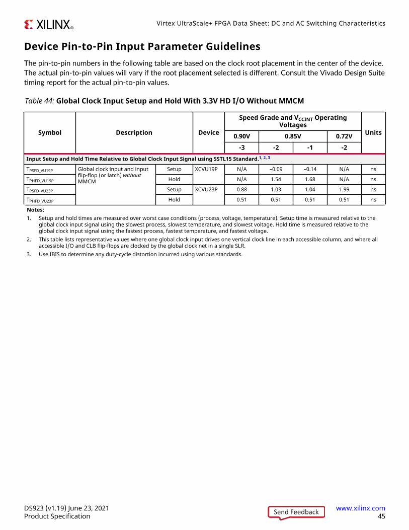
Device Pin-to-Pin Input Parameter GuidelinesThe pin-to-pin numbers in the following table are based on the clock root placement in the center of the device.The actual pin-to-pin values will vary if the root placement selected is different. Consult the Vivado Design Suitetiming report for the actual pin-to-pin values.
Table 44: Global Clock Input Setup and Hold With 3.3V HD I/O Without MMCM
Symbol Description Device
Speed Grade and VCCINT OperatingVoltages
Units0.90V 0.85V 0.72V-3 -2 -1 -2
Input Setup and Hold Time Relative to Global Clock Input Signal using SSTL15 Standard.1, 2, 3
TPSFD_VU19P Global clock input and inputflip-flop (or latch) withoutMMCM
Setup XCVU19P N/A –0.09 –0.14 N/A ns
TPHFD_VU19P Hold N/A 1.54 1.68 N/A ns
TPSFD_VU23P Setup XCVU23P 0.88 1.03 1.04 1.99 ns
TPHFD_VU23P Hold 0.51 0.51 0.51 0.51 ns
Notes:1. Setup and hold times are measured over worst case conditions (process, voltage, temperature). Setup time is measured relative to the
global clock input signal using the slowest process, slowest temperature, and slowest voltage. Hold time is measured relative to theglobal clock input signal using the fastest process, fastest temperature, and fastest voltage.
2. This table lists representative values where one global clock input drives one vertical clock line in each accessible column, and where allaccessible I/O and CLB flip-flops are clocked by the global clock net in a single SLR.
3. Use IBIS to determine any duty-cycle distortion incurred using various standards.
Virtex UltraScale+ FPGA Data Sheet: DC and AC Switching Characteristics
DS923 (v1.19) June 23, 2021 www.xilinx.comProduct Specification 45Send Feedback
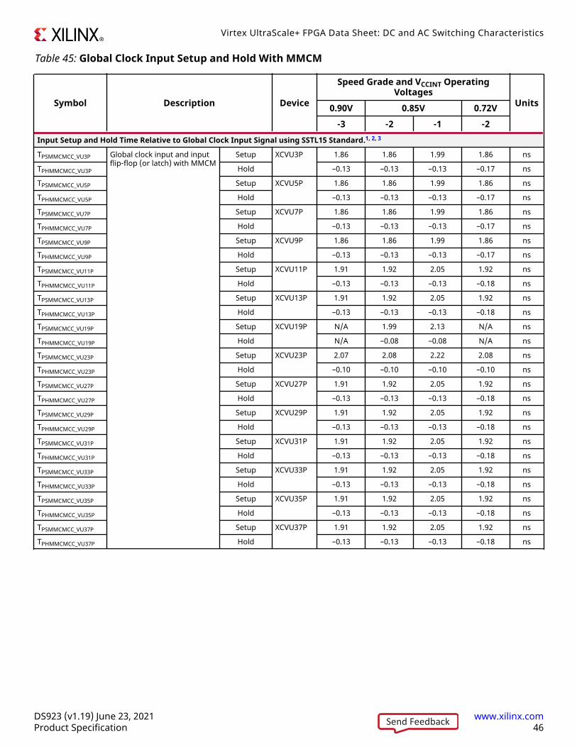
Table 45: Global Clock Input Setup and Hold With MMCM
Symbol Description Device
Speed Grade and VCCINT OperatingVoltages
Units0.90V 0.85V 0.72V-3 -2 -1 -2
Input Setup and Hold Time Relative to Global Clock Input Signal using SSTL15 Standard.1, 2, 3
TPSMMCMCC_VU3P Global clock input and inputflip-flop (or latch) with MMCM
Setup XCVU3P 1.86 1.86 1.99 1.86 ns
TPHMMCMCC_VU3P Hold –0.13 –0.13 –0.13 –0.17 ns
TPSMMCMCC_VU5P Setup XCVU5P 1.86 1.86 1.99 1.86 ns
TPHMMCMCC_VU5P Hold –0.13 –0.13 –0.13 –0.17 ns
TPSMMCMCC_VU7P Setup XCVU7P 1.86 1.86 1.99 1.86 ns
TPHMMCMCC_VU7P Hold –0.13 –0.13 –0.13 –0.17 ns
TPSMMCMCC_VU9P Setup XCVU9P 1.86 1.86 1.99 1.86 ns
TPHMMCMCC_VU9P Hold –0.13 –0.13 –0.13 –0.17 ns
TPSMMCMCC_VU11P Setup XCVU11P 1.91 1.92 2.05 1.92 ns
TPHMMCMCC_VU11P Hold –0.13 –0.13 –0.13 –0.18 ns
TPSMMCMCC_VU13P Setup XCVU13P 1.91 1.92 2.05 1.92 ns
TPHMMCMCC_VU13P Hold –0.13 –0.13 –0.13 –0.18 ns
TPSMMCMCC_VU19P Setup XCVU19P N/A 1.99 2.13 N/A ns
TPHMMCMCC_VU19P Hold N/A –0.08 –0.08 N/A ns
TPSMMCMCC_VU23P Setup XCVU23P 2.07 2.08 2.22 2.08 ns
TPHMMCMCC_VU23P Hold –0.10 –0.10 –0.10 –0.10 ns
TPSMMCMCC_VU27P Setup XCVU27P 1.91 1.92 2.05 1.92 ns
TPHMMCMCC_VU27P Hold –0.13 –0.13 –0.13 –0.18 ns
TPSMMCMCC_VU29P Setup XCVU29P 1.91 1.92 2.05 1.92 ns
TPHMMCMCC_VU29P Hold –0.13 –0.13 –0.13 –0.18 ns
TPSMMCMCC_VU31P Setup XCVU31P 1.91 1.92 2.05 1.92 ns
TPHMMCMCC_VU31P Hold –0.13 –0.13 –0.13 –0.18 ns
TPSMMCMCC_VU33P Setup XCVU33P 1.91 1.92 2.05 1.92 ns
TPHMMCMCC_VU33P Hold –0.13 –0.13 –0.13 –0.18 ns
TPSMMCMCC_VU35P Setup XCVU35P 1.91 1.92 2.05 1.92 ns
TPHMMCMCC_VU35P Hold –0.13 –0.13 –0.13 –0.18 ns
TPSMMCMCC_VU37P Setup XCVU37P 1.91 1.92 2.05 1.92 ns
TPHMMCMCC_VU37P Hold –0.13 –0.13 –0.13 –0.18 ns
Virtex UltraScale+ FPGA Data Sheet: DC and AC Switching Characteristics
DS923 (v1.19) June 23, 2021 www.xilinx.comProduct Specification 46Send Feedback

Table 45: Global Clock Input Setup and Hold With MMCM (cont'd)
Symbol Description Device
Speed Grade and VCCINT OperatingVoltages
Units0.90V 0.85V 0.72V-3 -2 -1 -2
TPSMMCMCC_VU45P Global clock input and inputflip-flop (or latch) with MMCM(cont'd)
Setup XCVU45P 1.91 1.92 2.05 1.92 ns
TPHMMCMCC_VU45P Hold –0.13 –0.13 –0.13 –0.18 ns
TPSMMCMCC_VU47P Setup XCVU47P 1.91 1.92 2.05 1.92 ns
TPHMMCMCC_VU47P Hold –0.13 –0.13 –0.13 –0.18 ns
TPSMMCMCC_VU57P Setup XCVU57P 1.91 1.92 2.05 1.92 ns
TPHMMCMCC_VU57P Hold –0.15 –0.13 –0.13 –0.18 ns
TPSMMCMCC_XQVU3P Setup XQVU3P N/A 1.86 1.99 1.86 ns
TPHMMCMCC_XQVU3P Hold N/A –0.13 –0.13 –0.17 ns
TPSMMCMCC_XQVU7P Setup XQVU7P N/A 1.86 1.99 1.86 ns
TPHMMCMCC_XQVU7P Hold N/A –0.13 –0.13 –0.17 ns
TPSMMCMCC_XQVU11P Setup XQVU11P N/A 1.92 2.05 1.92 ns
TPHMMCMCC_XQVU11P Hold N/A –0.13 –0.13 –0.18 ns
Notes:1. Setup and hold times are measured over worst case conditions (process, voltage, temperature). Setup time is measured relative to the
global clock input signal using the slowest process, slowest temperature, and slowest voltage. Hold time is measured relative to theglobal clock input signal using the fastest process, fastest temperature, and fastest voltage.
2. This table lists representative values where one global clock input drives one vertical clock line in each accessible column, and where allaccessible I/O and CLB flip-flops are clocked by the global clock net in a single SLR.
3. Use IBIS to determine any duty-cycle distortion incurred using various standards.
Table 46: Sampling Window
DescriptionSpeed Grade and VCCINT Operating Voltages
Units0.90V 0.85V 0.72V-3 -2 -1 -2
TSAMP_BUFG1 510 610 610 610 ps
TSAMP_NATIVE_DPA2 100 100 125 125 ps
TSAMP_NATIVE_BISC3 60 60 85 85 ps
Notes:1. This parameter indicates the total sampling error of the Virtex UltraScale+ FPGA DDR input registers, measured across voltage,
temperature, and process. The characterization methodology uses the MMCM to capture the DDR input registers' edges of operation.These measurements include: CLK0 MMCM jitter, MMCM accuracy (phase offset), and MMCM phase shift resolution. Thesemeasurements do not include package or clock tree skew.
2. This parameter is the receive sampling error for RX_BITSLICE when using dynamic phase alignment.3. This parameter is the receive sampling error for RX_BITSLICE when using built-in self-calibration (BISC).
Virtex UltraScale+ FPGA Data Sheet: DC and AC Switching Characteristics
DS923 (v1.19) June 23, 2021 www.xilinx.comProduct Specification 47Send Feedback
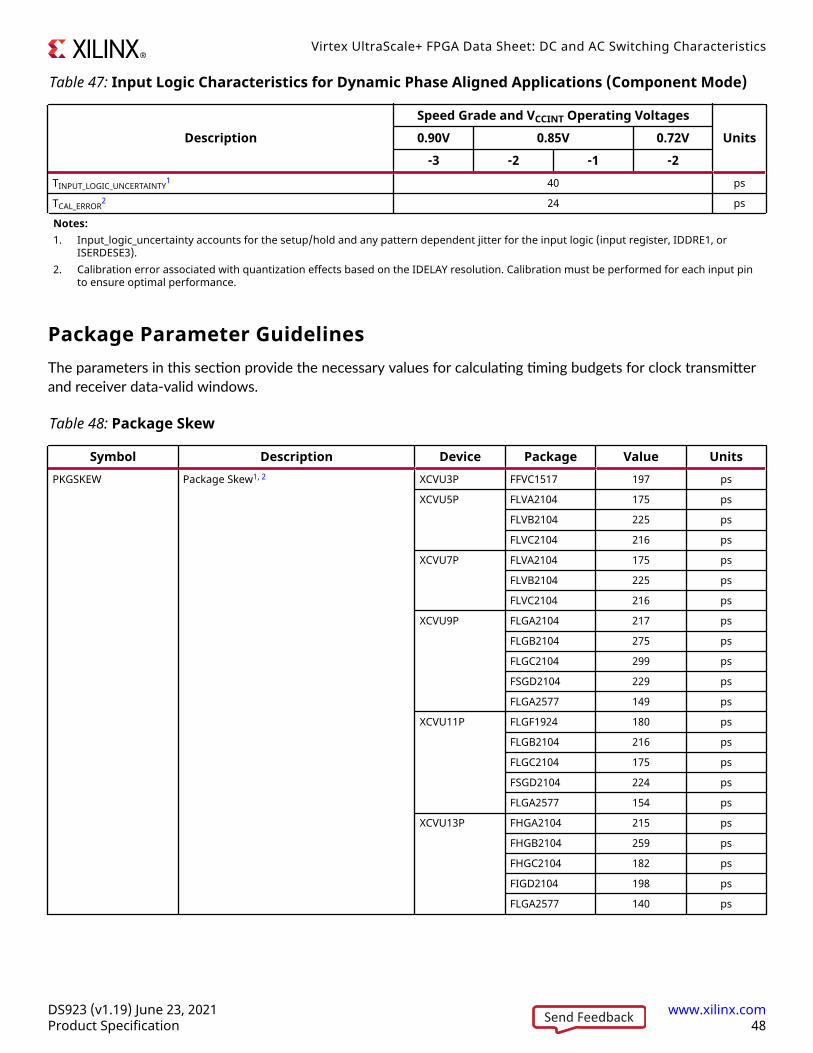
Table 47: Input Logic Characteristics for Dynamic Phase Aligned Applications (Component Mode)
DescriptionSpeed Grade and VCCINT Operating Voltages
Units0.90V 0.85V 0.72V-3 -2 -1 -2
TINPUT_LOGIC_UNCERTAINTY1 40 ps
TCAL_ERROR2 24 ps
Notes:1. Input_logic_uncertainty accounts for the setup/hold and any pattern dependent jitter for the input logic (input register, IDDRE1, or
ISERDESE3).2. Calibration error associated with quantization effects based on the IDELAY resolution. Calibration must be performed for each input pin
to ensure optimal performance.
Package Parameter GuidelinesThe parameters in this section provide the necessary values for calculating timing budgets for clock transmitterand receiver data-valid windows.
Table 48: Package Skew
Symbol Description Device Package Value UnitsPKGSKEW Package Skew1, 2 XCVU3P FFVC1517 197 ps
XCVU5P FLVA2104 175 ps
FLVB2104 225 ps
FLVC2104 216 ps
XCVU7P FLVA2104 175 ps
FLVB2104 225 ps
FLVC2104 216 ps
XCVU9P FLGA2104 217 ps
FLGB2104 275 ps
FLGC2104 299 ps
FSGD2104 229 ps
FLGA2577 149 ps
XCVU11P FLGF1924 180 ps
FLGB2104 216 ps
FLGC2104 175 ps
FSGD2104 224 ps
FLGA2577 154 ps
XCVU13P FHGA2104 215 ps
FHGB2104 259 ps
FHGC2104 182 ps
FIGD2104 198 ps
FLGA2577 140 ps
Virtex UltraScale+ FPGA Data Sheet: DC and AC Switching Characteristics
DS923 (v1.19) June 23, 2021 www.xilinx.comProduct Specification 48Send Feedback

Table 48: Package Skew (cont'd)
Symbol Description Device Package Value UnitsPKGSKEW (cont'd) Package Skew (cont'd)1, 2 XCVU19P FSVA3824 323 ps
FSVB3824 246 ps
XCVU23P VSVA1365 134 ps
FSVJ1760 187 ps
XCVU27P FIGD2104 198 ps
FSGA2577 139 ps
XCVU29P FIGD2104 198 ps
FSGA2577 139 ps
XCVU31P FSVH1924 165 ps
XCVU33P FSVH2104 194 ps
XCVU35P FSVH2104 200 ps
FSVH2892 241 ps
XCVU37P FSVH2892 278 ps
XCVU45P FSVH2104 200 ps
FSVH2892 241 ps
XCVU47P FSVH2892 278 ps
XCVU57P FSVK2892 278 ps
XQVU3P FFRC1517 176 ps
XQVU7P FLRA2104 175 ps
FLRB2104 224 ps
XQVU11P FLRC2104 174 ps
Notes:1. These values represent the worst-case skew between any two SelectIO resources in the package: shortest delay to longest delay from die
pad to ball.2. Package delay information is available for these device/package combinations. This information can be used to deskew the package.
GTY Transceiver SpecificationsThe UltraScale Architecture and Product Data Sheet: Overview (DS890) lists the Virtex UltraScale+ FPGAs thatinclude the GTY transceivers.
GTY Transceiver DC Input and Output LevelsTable 49 summarizes the DC specifications of the GTY transceivers in Virtex UltraScale+ FPGAs. Consult theUltraScale Architecture GTY Transceivers User Guide (UG578) for further details.
Table 49: GTY Transceiver DC Specifications
Symbol DC Parameter Conditions Min Typ Max UnitsDVPPIN Differential peak-to-peak input voltage
(external AC coupled)>10.3125 Gb/s 150 – 1250 mV
6.6 Gb/s to 10.3125 Gb/s 150 – 1250 mV
≤ 6.6 Gb/s 150 – 2000 mV
Virtex UltraScale+ FPGA Data Sheet: DC and AC Switching Characteristics
DS923 (v1.19) June 23, 2021 www.xilinx.comProduct Specification 49Send Feedback

Table 49: GTY Transceiver DC Specifications (cont'd)
Symbol DC Parameter Conditions Min Typ Max UnitsVIN Single-ended input voltage. Voltage
measured at the pin referenced toGND.
DC coupled VMGTAVTT = 1.2V –400 – VMGTAVTT mV
VCMIN Common mode input voltage DC coupled VMGTAVTT = 1.2V – 2/3 VMGTAVTT – mV
DVPPOUT Differential peak-to-peak outputvoltage1
Transmitter output swing is setto 11111
800 – – mV
VCMOUTDC Common mode output voltage: DCcoupled (equation based)
When remote RX is terminated toGND
VMGTAVTT/2 – DVPPOUT/4 mV
When remote RX termination isfloating
VMGTAVTT – DVPPOUT/2 mV
When remote RX is terminated toVRX_TERM2
mV
VCMOUTAC Common mode output voltage: ACcoupled
Equation based VMGTAVTT – DVPPOUT/2 mV
RIN Differential input resistance – 100 – Ω
ROUT Differential output resistance – 100 – Ω
TOSKEW Transmitter output pair (TXP and TXN) intra-pair skew – – 10 ps
CEXT Recommended external AC coupling capacitor3 – 100 – nF
Notes:1. The output swing and pre-emphasis levels are programmable using the GTY transceiver attributes discussed in the UltraScale Architecture
GTY Transceivers User Guide (UG578) and can result in values lower than reported in this table.2. VRX_TERM is the remote RX termination voltage.3. Other values can be used as appropriate to conform to specific protocols and standards.
Figure 3: Single-Ended Peak-to-Peak Voltage
0
+V P
N
Single-Ended Peak-to-PeakVoltage
X16653-072117
Figure 4: Differential Peak-to-Peak Voltage
0
+V
–V P–N
Differential Peak-to-Peak
Voltage
Differential peak-to-peak voltage = (Single-ended peak-to-peak voltage) x 2X16639-072117
The following tables summarize the DC specifications of the clock input/output levels of the GTY transceivers inVirtex UltraScale+ FPGAs. Consult the UltraScale Architecture GTY Transceivers User Guide (UG578) for furtherdetails.
Virtex UltraScale+ FPGA Data Sheet: DC and AC Switching Characteristics
DS923 (v1.19) June 23, 2021 www.xilinx.comProduct Specification 50Send Feedback

Table 50: GTY Transceiver Clock DC Input Level Specification
Symbol DC Parameter Min Typ Max UnitsVIDIFF Differential peak-to-peak input voltage 250 – 2000 mV
RIN Differential input resistance – 100 – Ω
CEXT Required external AC coupling capacitor – 10 – nF
Table 51: GTY Transceiver Clock Output Level Specification
Symbol Description Conditions Min Typ Max UnitsVOL Output Low voltage for P and N RT = 100Ω across P and N signals 100 – 330 mV
VOH Output High voltage for P and N RT = 100Ω across P and N signals 500 – 700 mV
VDDOUT Differential output voltage (P–N), P = High (N–P), N = High
RT = 100Ω across P and N signals 300 – 430 mV
VCMOUT Common mode voltage RT = 100Ω across P and N signals 300 – 500 mV
GTY Transceiver Switching CharacteristicsConsult the UltraScale Architecture GTY Transceivers User Guide (UG578) for further information.
Table 52: GTY Transceiver Performance
Symbol Description OutputDivider
Speed Grade and VCCINT Operating VoltagesUnits0.90V 0.85V 0.72V
-3 -2 -1 -2FGTYMAX GTY maximum line rate 32.751, 2 28.211, 2 25.7851, 2 28.211, 2 Gb/s
FGTYMIN GTY minimum line rate 0.5 0.5 0.5 0.5 Gb/s
Min Max Min Max Min Max Min Max
FGTYCRANGE CPLL line raterange3
1 4.0 12.5 4.0 12.5 4.0 8.5 4.0 12.5 Gb/s
2 2.0 6.25 2.0 6.25 2.0 4.25 2.0 6.25 Gb/s
4 1.0 3.125 1.0 3.125 1.0 2.125 1.0 3.125 Gb/s
8 0.5 1.5625 0.5 1.5625 0.5 1.0625 0.5 1.5625 Gb/s
16 N/A Gb/s
32 N/A Gb/s
Min Max Min Max Min Max Min Max
FGTYQRANGE1 QPLL0 line raterange4
1 19.6 32.75 19.6 28.21 19.6 25.785 19.6 28.21 Gb/s
1 9.8 16.375 9.8 16.375 9.8 16.375 9.8 16.375 Gb/s
2 4.9 8.1875 4.9 8.1875 4.9 8.1875 4.9 8.1875 Gb/s
4 2.45 4.0938 2.45 4.0938 2.45 4.0938 2.45 4.0938 Gb/s
8 1.225 2.0469 1.225 2.0469 1.225 2.0469 1.225 2.0469 Gb/s
16 0.6125 1.0234 0.6125 1.0234 0.6125 1.0234 0.6125 1.0234 Gb/s
Virtex UltraScale+ FPGA Data Sheet: DC and AC Switching Characteristics
DS923 (v1.19) June 23, 2021 www.xilinx.comProduct Specification 51Send Feedback

Table 52: GTY Transceiver Performance (cont'd)
Symbol Description OutputDivider
Speed Grade and VCCINT Operating VoltagesUnits0.90V 0.85V 0.72V
-3 -2 -1 -2Min Max Min Max Min Max Min Max
FGTYQRANGE2 QPLL1 line raterange5
1 16.0 26.0 16.0 26.0 16.0 25.785 16.0 26.0 Gb/s
1 8.0 13.0 8.0 13.0 8.0 12.5 8.0 13.0 Gb/s
2 4.0 6.5 4.0 6.5 4.0 6.5 4.0 6.5 Gb/s
4 2.0 3.25 2.0 3.25 2.0 3.25 2.0 3.25 Gb/s
8 1.0 1.625 1.0 1.625 1.0 1.625 1.0 1.625 Gb/s
16 0.5 0.8125 0.5 0.8125 0.5 0.8125 0.5 0.8125 Gb/s
Min Max Min Max Min Max Min Max
FCPLLRANGE CPLL frequency range 2.0 6.25 2.0 6.25 2.0 4.25 2.0 6.25 GHz
FQPLL0RANGE QPLL0 frequency range 9.8 16.375 9.8 16.375 9.8 16.375 9.8 16.375 GHz
FQPLL1RANGE QPLL1 frequency range 8.0 13.0 8.0 13.0 8.0 13.0 8.0 13.0 GHz
Notes:1. XCVU23P devices in the VSVA1365 package have a maximum GTY transceiver line rate of 25.785 Gb/s in GTY Quad 231 and a maximum
GTY transceiver line rate of 16.3 Gb/s in the other GTY Quads.2. XCVU11P devices in the FLGF1924 package have a maximum GTY transceiver line rate of 16.3 Gb/s.3. The values listed are the rounded results of the calculated equation (2 × CPLL_Frequency)/Output_Divider.4. The values listed are the rounded results of the calculated equation (QPLL0_Frequency × RATE)/Output_Divider where RATE is 1 when
QPLL0_CLKOUT_RATE is set to HALF and 2 if QPLL0_CLKOUT_RATE is set to FULL.5. The values listed are the rounded results of the calculated equation (QPLL1_Frequency × RATE)/Output_Divider where RATE is 1 when
QPLL1_CLKOUT_RATE is set to HALF and 2 if QPLL1_CLKOUT_RATE is set to FULL.
Table 53: GTY Transceiver Dynamic Reconfiguration Port (DRP) Switching Characteristics
Symbol Description All Speed Grades UnitsFGTYDRPCLK GTYDRPCLK maximum frequency 250 MHz
Table 54: GTY Transceiver Reference Clock Switching Characteristics
Symbol Description ConditionsAll Speed Grades
UnitsMin Typ Max
FGCLK Reference clock frequency range 60 – 820 MHz
TRCLK Reference clock rise time 20% – 80% – 200 – ps
TFCLK Reference clock fall time 80% – 20% – 200 – ps
TDCREF Reference clock duty cycle Transceiver PLL only 40 50 60 %
Virtex UltraScale+ FPGA Data Sheet: DC and AC Switching Characteristics
DS923 (v1.19) June 23, 2021 www.xilinx.comProduct Specification 52Send Feedback
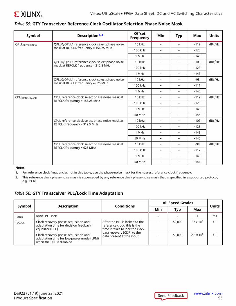
Table 55: GTY Transceiver Reference Clock Oscillator Selection Phase Noise Mask
Symbol Description1, 2 OffsetFrequency Min Typ Max Units
QPLLREFCLKMASK QPLL0/QPLL1 reference clock select phase noisemask at REFCLK frequency = 156.25 MHz
10 kHz – – –112 dBc/Hz
100 kHz – – –128
1 MHz – – –145
QPLL0/QPLL1 reference clock select phase noisemask at REFCLK frequency = 312.5 MHz
10 kHz – – –103 dBc/Hz
100 kHz – – –123
1 MHz – – –143
QPLL0/QPLL1 reference clock select phase noisemask at REFCLK frequency = 625 MHz
10 kHz – – –98 dBc/Hz
100 kHz – – –117
1 MHz – – –140
CPLLREFCLKMASK CPLL reference clock select phase noise mask atREFCLK frequency = 156.25 MHz
10 kHz – – –112 dBc/Hz
100 kHz – – –128
1 MHz – – –145
50 MHz – – –145
CPLL reference clock select phase noise mask atREFCLK frequency = 312.5 MHz
10 kHz – – –103 dBc/Hz
100 kHz – – –123
1 MHz – – –143
50 MHz – – –145
CPLL reference clock select phase noise mask atREFCLK frequency = 625 MHz
10 kHz – – –98 dBc/Hz
100 kHz – – –117
1 MHz – – –140
50 MHz – – –144
Notes:1. For reference clock frequencies not in this table, use the phase-noise mask for the nearest reference clock frequency.2. This reference clock phase-noise mask is superseded by any reference clock phase-noise mask that is specified in a supported protocol,
e.g., PCIe.
Table 56: GTY Transceiver PLL/Lock Time Adaptation
Symbol Description ConditionsAll Speed Grades
UnitsMin Typ Max
TLOCK Initial PLL lock. – – 1 ms
TDLOCK Clock recovery phase acquisition andadaptation time for decision feedbackequalizer (DFE)
After the PLL is locked to thereference clock, this is thetime it takes to lock the clockdata recovery (CDR) to thedata present at the input.
– 50,000 37 x 106 UI
Clock recovery phase acquisition andadaptation time for low-power mode (LPM)when the DFE is disabled
– 50,000 2.3 x 10⁶ UI
Virtex UltraScale+ FPGA Data Sheet: DC and AC Switching Characteristics
DS923 (v1.19) June 23, 2021 www.xilinx.comProduct Specification 53Send Feedback
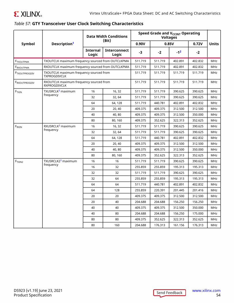
Table 57: GTY Transceiver User Clock Switching Characteristics
Symbol Description1
Data Width Conditions(Bit)
Speed Grade and VCCINT OperatingVoltages
Units0.90V 0.85V 0.72VInternal
LogicInterconnect
Logic -3 -2 -12 -2
FTXOUTPMA TXOUTCLK maximum frequency sourced from OUTCLKPMA 511.719 511.719 402.891 402.832 MHz
FRXOUTPMA RXOUTCLK maximum frequency sourced from OUTCLKPMA 511.719 511.719 402.891 402.832 MHz
FTXOUTPROGDIV TXOUTCLK maximum frequency sourced fromTXPROGDIVCLK
511.719 511.719 511.719 511.719 MHz
FRXOUTPROGDIV RXOUTCLK maximum frequency sourced fromRXPROGDIVCLK
511.719 511.719 511.719 511.719 MHz
FTXIN TXUSRCLK3 maximumfrequency
16 16, 32 511.719 511.719 390.625 390.625 MHz
32 32, 64 511.719 511.719 390.625 390.625 MHz
64 64, 128 511.719 440.781 402.891 402.832 MHz
20 20, 40 409.375 409.375 312.500 312.500 MHz
40 40, 80 409.375 409.375 312.500 350.000 MHz
80 80, 160 409.375 352.625 322.313 352.625 MHz
FRXIN RXUSRCLK3 maximumfrequency
16 16, 32 511.719 511.719 390.625 390.625 MHz
32 32, 64 511.719 511.719 390.625 390.625 MHz
64 64, 128 511.719 440.781 402.891 402.832 MHz
20 20, 40 409.375 409.375 312.500 312.500 MHz
40 40, 80 409.375 409.375 312.500 350.000 MHz
80 80, 160 409.375 352.625 322.313 352.625 MHz
FTXIN2 TXUSRCLK23 maximumfrequency
16 16 511.719 511.719 390.625 390.625 MHz
16 32 255.859 255.859 195.313 195.313 MHz
32 32 511.719 511.719 390.625 390.625 MHz
32 64 255.859 255.859 195.313 195.313 MHz
64 64 511.719 440.781 402.891 402.832 MHz
64 128 255.859 220.391 201.445 201.416 MHz
20 20 409.375 409.375 312.500 312.500 MHz
20 40 204.688 204.688 156.250 156.250 MHz
40 40 409.375 409.375 312.500 350.000 MHz
40 80 204.688 204.688 156.250 175.000 MHz
80 80 409.375 352.625 322.313 352.625 MHz
80 160 204.688 176.313 161.156 176.313 MHz
Virtex UltraScale+ FPGA Data Sheet: DC and AC Switching Characteristics
DS923 (v1.19) June 23, 2021 www.xilinx.comProduct Specification 54Send Feedback

Table 57: GTY Transceiver User Clock Switching Characteristics (cont'd)
Symbol Description1
Data Width Conditions(Bit)
Speed Grade and VCCINT OperatingVoltages
Units0.90V 0.85V 0.72VInternal
LogicInterconnect
Logic -3 -2 -12 -2
FRXIN2 RXUSRCLK23 maximumfrequency
16 16 511.719 511.719 390.625 390.625 MHz
16 32 255.859 255.859 195.313 195.313 MHz
32 32 511.719 511.719 390.625 390.625 MHz
32 64 255.859 255.859 195.313 195.313 MHz
64 64 511.719 440.781 402.891 402.832 MHz
64 128 255.859 220.391 201.445 201.416 MHz
20 20 409.375 409.375 312.500 312.500 MHz
20 40 204.688 204.688 156.250 156.250 MHz
40 40 409.375 409.375 312.500 350.000 MHz
40 80 204.688 204.688 156.250 175.000 MHz
80 80 409.375 352.625 322.313 352.625 MHz
80 160 204.688 176.313 161.156 176.313 MHz
Notes:1. Clocking must be implemented as described in the UltraScale Architecture GTY Transceivers User Guide (UG578).2. For the speed grades -1E, -1I, and -1M, only a 64- or 80-bit internal data path can be used for line rates above 12.5 Gb/s.3. When the gearbox is used, these maximums refer to the XCLK. For more information, see the Valid Data Width Combinations for TX
Asynchronous Gearbox table in the UltraScale Architecture GTY Transceivers User Guide (UG578).
Table 58: GTY Transceiver Transmitter Switching Characteristics
Symbol Description Condition Min Typ Max UnitsFGTYTX Serial data rate range 0.500 – FGTYMAX Gb/s
TRTX TX rise time 20%–80% – 21 – ps
TFTX TX fall time 80%–20% – 21 – ps
TLLSKEW TX lane-to-lane skew1 – – 500.00 ps
TJ32.75 Total jitter2, 4 32.75 Gb/s – – 0.35 UI
DJ32.75 Deterministic jitter2, 4 – – 0.19 UI
TJ28.21 Total jitter2, 4 28.21 Gb/s – – 0.28 UI
DJ28.21 Deterministic jitter2, 4 – – 0.17 UI
TJ16.375 Total jitter2, 4 16.375 Gb/s – – 0.28 UI
DJ16.375 Deterministic jitter2, 4 – – 0.17 UI
TJ15.0 Total jitter2, 4 15.0 Gb/s – – 0.28 UI
DJ15.0 Deterministic jitter2, 4 – – 0.17 UI
TJ14.1 Total jitter2, 4 14.1 Gb/s – – 0.28 UI
DJ14.1 Deterministic jitter2, 4 – – 0.17 UI
TJ14.1 Total jitter2, 4 14.025 Gb/s – – 0.28 UI
DJ14.1 Deterministic jitter2, 4 – – 0.17 UI
Virtex UltraScale+ FPGA Data Sheet: DC and AC Switching Characteristics
DS923 (v1.19) June 23, 2021 www.xilinx.comProduct Specification 55Send Feedback
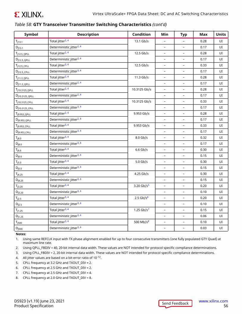
Table 58: GTY Transceiver Transmitter Switching Characteristics (cont'd)
Symbol Description Condition Min Typ Max UnitsTJ13.1 Total jitter2, 4 13.1 Gb/s – – 0.28 UI
DJ13.1 Deterministic jitter2, 4 – – 0.17 UI
TJ12.5_QPLL Total jitter2, 4 12.5 Gb/s – – 0.28 UI
DJ12.5_QPLL Deterministic jitter2, 4 – – 0.17 UI
TJ12.5_CPLL Total jitter3, 4 12.5 Gb/s – – 0.33 UI
DJ12.5_CPLL Deterministic jitter3, 4 – – 0.17 UI
TJ11.3_QPLL Total jitter2, 4 11.3 Gb/s – – 0.28 UI
DJ11.3_QPLL Deterministic jitter2, 4 – – 0.17 UI
TJ10.3125_QPLL Total jitter2, 4 10.3125 Gb/s – – 0.28 UI
DJ10.3125_QPLL Deterministic jitter2, 4 – – 0.17 UI
TJ10.3125_CPLL Total jitter3, 4 10.3125 Gb/s – – 0.33 UI
DJ10.3125_CPLL Deterministic jitter3, 4 – – 0.17 UI
TJ9.953_QPLL Total jitter2, 4 9.953 Gb/s – – 0.28 UI
DJ9.953_QPLL Deterministic jitter2, 4 – – 0.17 UI
TJ9.953_CPLL Total jitter3, 4 9.953 Gb/s – – 0.33 UI
DJ9.953_CPLL Deterministic jitter3, 4 – – 0.17 UI
TJ8.0 Total jitter3, 4 8.0 Gb/s – – 0.32 UI
DJ8.0 Deterministic jitter3, 4 – – 0.17 UI
TJ6.6 Total jitter3, 4 6.6 Gb/s – – 0.30 UI
DJ6.6 Deterministic jitter3, 4 – – 0.15 UI
TJ5.0 Total jitter3, 4 5.0 Gb/s – – 0.30 UI
DJ5.0 Deterministic jitter3, 4 – – 0.15 UI
TJ4.25 Total jitter3, 4 4.25 Gb/s – – 0.30 UI
DJ4.25 Deterministic jitter3, 4 – – 0.15 UI
TJ3.20 Total jitter3, 4 3.20 Gb/s5 – – 0.20 UI
DJ3.20 Deterministic jitter3, 4 – – 0.10 UI
TJ2.5 Total jitter3, 4 2.5 Gb/s6 – – 0.20 UI
DJ2.5 Deterministic jitter3, 4 – – 0.10 UI
TJ1.25 Total jitter3, 4 1.25 Gb/s7 – – 0.15 UI
DJ1.25 Deterministic jitter3, 4 – – 0.06 UI
TJ500 Total jitter3, 4 500 Mb/s8 – – 0.10 UI
DJ500 Deterministic jitter3, 4 – – 0.03 UI
Notes:1. Using same REFCLK input with TX phase alignment enabled for up to four consecutive transmitters (one fully populated GTY Quad) at
maximum line rate.2. Using QPLL_FBDIV = 40, 20-bit internal data width. These values are NOT intended for protocol specific compliance determinations.3. Using CPLL_FBDIV = 2, 20-bit internal data width. These values are NOT intended for protocol specific compliance determinations.4. All jitter values are based on a bit-error ratio of 10–12.5. CPLL frequency at 3.2 GHz and TXOUT_DIV = 2.6. CPLL frequency at 2.5 GHz and TXOUT_DIV = 2.7. CPLL frequency at 2.5 GHz and TXOUT_DIV = 4.8. CPLL frequency at 2.0 GHz and TXOUT_DIV = 8.
Virtex UltraScale+ FPGA Data Sheet: DC and AC Switching Characteristics
DS923 (v1.19) June 23, 2021 www.xilinx.comProduct Specification 56Send Feedback

Table 59: GTY Transceiver Receiver Switching Characteristics
Symbol Description Condition Min Typ Max UnitsFGTYRX Serial data rate 0.500 – FGTYMAX Gb/s
RXSST Receiver spread-spectrum tracking1 Modulated at 33 kHz –5000 – 0 ppm
RXRL Run length (CID) – – 256 UI
RXPPMTOL Data/REFCLK PPM offset tolerance Bit rates ≤ 6.6 Gb/s –1250 – 1250 ppm
Bit rates > 6.6 Gb/s and≤ 8.0 Gb/s
–700 – 700 ppm
Bit rates > 8.0 Gb/s –200 – 200 ppm
SJ Jitter Tolerance2
JT_SJ32.75 Sinusoidal jitter (QPLL)3 32.75 Gb/s 0.25 – – UI
JT_SJ28.21 Sinusoidal jitter (QPLL)3 28.21 Gb/s 0.30 – – UI
JT_SJ16.375 Sinusoidal jitter (QPLL)3 16.375 Gb/s 0.30 – – UI
JT_SJ15.0 Sinusoidal jitter (QPLL)3 15.0 Gb/s 0.30 – – UI
JT_SJ14.1 Sinusoidal jitter (QPLL)3 14.1 Gb/s 0.30 – – UI
JT_SJ13.1 Sinusoidal jitter (QPLL)3 13.1 Gb/s 0.30 – – UI
JT_SJ12.5 Sinusoidal jitter (QPLL)3 12.5 Gb/s 0.30 – – UI
JT_SJ11.3 Sinusoidal jitter (QPLL)3 11.3 Gb/s 0.30 – – UI
JT_SJ10.32_QPLL Sinusoidal jitter (QPLL)3 10.32 Gb/s 0.30 – – UI
JT_SJ10.32_CPLL Sinusoidal jitter (CPLL)3 10.32 Gb/s 0.30 – – UI
JT_SJ9.953_QPLL Sinusoidal jitter (QPLL)3 9.953 Gb/s 0.30 – – UI
JT_SJ9.953_CPLL Sinusoidal jitter (CPLL)3 9.953 Gb/s 0.30 – – UI
JT_SJ8.0 Sinusoidal jitter (CPLL)3 8.0 Gb/s 0.42 – – UI
JT_SJ6.6 Sinusoidal jitter (CPLL)3 6.6 Gb/s 0.44 – – UI
JT_SJ5.0 Sinusoidal jitter (CPLL)3 5.0 Gb/s 0.44 – – UI
JT_SJ4.25 Sinusoidal jitter (CPLL)3 4.25 Gb/s 0.44 – – UI
JT_SJ3.2 Sinusoidal jitter (CPLL)3 3.2 Gb/s4 0.45 – – UI
JT_SJ2.5 Sinusoidal jitter (CPLL)3 2.5 Gb/s5 0.30 – – UI
JT_SJ1.25 Sinusoidal jitter (CPLL)3 1.25 Gb/s6 0.30 – – UI
JT_SJ500 Sinusoidal jitter (CPLL)3 500 Mb/s7 0.30 – – UI
SJ Jitter Tolerance with Stressed Eye2
JT_TJSE3.2 Total jitter with stressed eye8 3.2 Gb/s 0.70 – – UI
JT_TJSE6.6 6.6 Gb/s 0.70 – – UI
JT_SJSE3.2 Sinusoidal jitter with stressed eye8 3.2 Gb/s 0.10 – – UI
JT_SJSE6.6 6.6 Gb/s 0.10 – – UI
Notes:1. Using RXOUT_DIV = 1, 2, and 4.2. All jitter values are based on a bit error ratio of 10–12.3. The frequency of the injected sinusoidal jitter is 80 MHz.4. CPLL frequency at 3.2 GHz and RXOUT_DIV = 2.5. CPLL frequency at 2.5 GHz and RXOUT_DIV = 2.6. CPLL frequency at 2.5 GHz and RXOUT_DIV = 4.7. CPLL frequency at 2.0 GHz and RXOUT_DIV = 8.8. Composite jitter with RX equalizer enabled. DFE disabled.
Virtex UltraScale+ FPGA Data Sheet: DC and AC Switching Characteristics
DS923 (v1.19) June 23, 2021 www.xilinx.comProduct Specification 57Send Feedback

GTY Transceiver Electrical ComplianceThe UltraScale Architecture GTY Transceivers User Guide (UG578) contains recommended use modes that ensurecompliance for the protocols listed in the following table. The transceiver wizard provides the recommendedsettings for those use cases and for protocol specific characteristics.
Table 60: GTY Transceiver Protocol List
Protocol Specification Serial Rate (Gb/s) ElectricalCompliance
CAUI-4 IEEE 802.3-2012 25.78125 Compliant
28 Gb/s backplane CEI-25G-LR 25–28.05 Compliant
Interlaken OIF-CEI-6G, OIF-CEI-11GSR, OIF-CEI-28G-MR 4.25–25.78125 Compliant
100GBASE-KR4 IEEE 802.3bj-2014, CEI-25G-LR 25.78125 Compliant1
100GBASE-CR4 IEEE 802.3bj-2014, CEI-25G-LR 25.78125 Compliant1
50GBASE-KR4 IEEE 802.3by-2014, CEI-25G-LR 25.78125 Compliant1
50GBASE-CR4 IEEE 802.3by-2014, CEI-25G-LR 25.78125 Compliant1
25GBASE-KR4 IEEE 802.3by-2014, CEI-25G-LR 25.78125 Compliant1
25GBASE-CR4 IEEE 802.3by-2014, CEI-25G-LR 25.78125 Compliant1
OTU4 (OTL4.4) CFP2 OIF-CEI-28G-VSR 27.952493–32.75 Compliant
OTU4 (OTL4.4) CFP OIF-CEI-11G-MR 11.18–13.1 Compliant
CAUI-10 IEEE 802.3-2012 10.3125 Compliant
nPPI IEEE 802.3-2012 10.3125 Compliant
10GBASE-KR2 IEEE 802.3-2012 10.3125 Compliant
SFP+ SFF-8431 (SR and LR) 9.95328–11.10 Compliant
XFP INF-8077i, revision 4.5 10.3125 Compliant
RXAUI CEI-6G-SR 6.25 Compliant
XAUI IEEE 802.3-2012 3.125 Compliant
1000BASE-X IEEE 802.3-2012 1.25 Compliant
5.0G Ethernet IEEE 802.3bx (PAR) 5 Compliant
2.5G Ethernet IEEE 802.3bx (PAR) 2.5 Compliant
HiGig, HiGig+, HiGig2 IEEE 802.3-2012 3.74, 6.6 Compliant
QSGMII QSGMII v1.2 (Cisco System, ENG-46158) 5 Compliant
OTU2 ITU G.8251 10.709225 Compliant
OTU4 (OTL4.10) OIF-CEI-11G-SR 11.180997 Compliant
OC-3/12/48/192 GR-253-CORE 0.1555–9.956 Compliant
PCIe Gen1, 2, 3 PCI Express base 3.0 2.5, 5.0, and 8.0 Compliant
SDI3 SMPTE 424M-2006 0.27–2.97 Compliant
UHD-SDI3 SMPTE ST-2081 6G, SMPTE ST-2082 12G 6 and 12 Compliant
Hybrid memory cube (HMC) HMC-15G-SR 10, 12.5, and 15.0 Compliant
MoSys bandwidth engine CEI-11-SR and CEI-11-SR (overclocked) 10.3125, 15.5 Compliant
CPRI CPRI_v_6_1_2014-07-01 0.6144–12.165 Compliant
Passive optical network (PON) 10G-EPON, 1G-EPON, NG-PON2, XG-PON, and 2.5G-PON 0.155–10.3125 Compliant
JESD204a/b OIF-CEI-6G, OIF-CEI-11G 3.125–12.5 Compliant
Serial RapidIO RapidIO specification 3.1 1.25–10.3125 Compliant
Virtex UltraScale+ FPGA Data Sheet: DC and AC Switching Characteristics
DS923 (v1.19) June 23, 2021 www.xilinx.comProduct Specification 58Send Feedback

Table 60: GTY Transceiver Protocol List (cont'd)
Protocol Specification Serial Rate (Gb/s) ElectricalCompliance
DisplayPort DP 1.2B CTS 1.62–5.4 Compliant3
Fibre channel FC-PI-4 1.0625–14.025 Compliant
SATA Gen1, 2, 3 Serial ATA revision 3.0 specification 1.5, 3.0, and 6.0 Compliant
SAS Gen1, 2, 3 T10/BSR INCITS 519 3.0, 6.0, and 12.0 Compliant
SFI-5 OIF-SFI5-01.0 0.625 - 12.5 Compliant
Aurora CEI-6G, CEI-11G-LR All rates Compliant
Notes:1. 25 dB loss at Nyquist without FEC.2. The transition time of the transmitter is faster than the IEEE Std 802.3-2012 specification.3. This protocol requires external circuitry to achieve compliance.
Virtex UltraScale+ FPGA Data Sheet: DC and AC Switching Characteristics
DS923 (v1.19) June 23, 2021 www.xilinx.comProduct Specification 59Send Feedback

GTM Transceiver SpecificationsThe UltraScale Architecture and Product Data Sheet: Overview (DS890) lists the Virtex UltraScale+ FPGAs thatinclude the GTM transceivers.
GTM Transceiver DC Input and Output LevelsTable 61 summarizes the DC specifications of the GTM transceivers in Virtex UltraScale+ FPGAs. Consult theVirtex UltraScale+ FPGAs GTM Transceivers User Guide (UG581) for further details.
Table 61: GTM Transceiver DC Specifications
Symbol DC Parameter Conditions Min Typ Max UnitsDVPPIN Differential peak-to-peak input voltage
(external AC coupled)PAM4 600 – 800 mV
NRZ 150 – 900 mV
DVPPOUT Differential peak-to-peak outputvoltage1
Transmitter output swing is setto 11111
800 – – mV
VCMOUTAC Common mode output voltage: ACcoupled
Equation based VMGTAVTT – DVPPOUT/2 mV
RIN Differential input resistance – 100 – Ω
ROUT Differential output resistance – 100 – Ω
TOSKEW Transmitter output pair (TXP and TXN) intra-pair skew – – 10 ps
CEXT Recommended external AC coupling capacitor3 – 100 – nF
Notes:1. The output swing and pre-emphasis levels are programmable using the GTM transceiver attributes discussed in the Virtex UltraScale+
FPGAs GTM Transceivers User Guide (UG581) and can result in values lower than reported in this table.2. VRX_TERM is the remote RX termination voltage.3. Other values can be used as appropriate to conform to specific protocols and standards.
Figure 5: Single-Ended Peak-to-Peak Voltage
0
+V P
N
Single-Ended Peak-to-PeakVoltage
X16653-072117
Figure 6: Differential Peak-to-Peak Voltage
0
+V
–V P–N
Differential Peak-to-Peak
Voltage
Differential peak-to-peak voltage = (Single-ended peak-to-peak voltage) x 2X16639-072117
Virtex UltraScale+ FPGA Data Sheet: DC and AC Switching Characteristics
DS923 (v1.19) June 23, 2021 www.xilinx.comProduct Specification 60Send Feedback

The following tables summarize the DC specifications of the clock input/output levels of the GTM transceiversin Virtex UltraScale+ FPGAs. Consult the Virtex UltraScale+ FPGAs GTM Transceivers User Guide (UG581) forfurther details.
Table 62: GTM Transceiver Clock DC Input Level Specification
Symbol DC Parameter Min Typ Max UnitsVIDIFF Differential peak-to-peak input voltage 250 – 2000 mV
RIN Differential input resistance – 100 – Ω
CEXT Required external AC coupling capacitor – 10 – nF
GTM Transceiver Switching CharacteristicsConsult the Virtex UltraScale+ FPGAs GTM Transceivers User Guide (UG581) for further information.
Table 63: GTM Transceiver Performance
Symbol Description1, 2 OutputDivider
Speed Grade and VCCINT OperatingVoltages
Units0.90V 0.85V 0.72V-3 -2 -1 -2
Max Max Max MaxFGTMPAM4MAX GTM transceiver PAM4 maximum line rate 1 58.00 56.42 53.20 56.42 Gb/s
FGTMPAM4MIN GTM transceiver PAM4 minimum line rate 39.20 39.20 39.20 39.20 Gb/s
FGTMPAM42MAX GTM transceiver PAM4 maximum line rate 2 29.00 28.21 26.60 28.21 Gb/s
FGTMPAM42MIN GTM transceiver PAM4 minimum line rate 20.60 20.60 20.60 20.60 Gb/s
FGTMNRZMAX GTM transceiver NRZ maximum line rate 1 29.00 28.21 26.60 28.21 Gb/s
FGTMNRZMIN GTM transceiver NRZ minimum line rate 19.60 19.60 19.60 19.60 Gb/s
FGTMNRZ2MAX GTM transceiver NRZ maximum line rate 2 14.50 14.105 13.30 14.105 Gb/s
FGTMNRZ2MIN GTM transceiver NRZ minimum line rate 10.30 10.30 10.30 10.30 Gb/s
Notes:1. For PAM4, data rates from FGTMPAM42MAX to 39.2 Gb/s are not available.2. For NRZ, data rates from FGTMNRZ2MAX to 19.6 Gb/s are not available.
Table 64: GTM Transceiver Dynamic Reconfiguration Port (DRP) Switching Characteristics
Symbol Description All Speed Grades UnitsFGTMDRPCLK GTMDRPCLK maximum frequency 250 MHz
Virtex UltraScale+ FPGA Data Sheet: DC and AC Switching Characteristics
DS923 (v1.19) June 23, 2021 www.xilinx.comProduct Specification 61Send Feedback

Table 65: GTM Transceiver Reference Clock Switching Characteristics
Symbol Description ConditionsAll Speed Grades
UnitsMin Typ Max
FGCLK Reference clock frequency range 60 – 820 MHz
TRCLK Reference clock rise time 20% – 80% – 200 – ps
TFCLK Reference clock fall time 80% – 20% – 200 – ps
TDCREF Reference clock duty cycle Transceiver PLL only 40 50 60 %
Table 66: GTM Transceiver Reference Clock Oscillator Selection Phase Noise Mask
Symbol Description1, 2 OffsetFrequency Min Typ Max Units
LCPLLREFCLKMASK LCPLL reference clock select phase noise mask atREFCLK frequency = 156.25 MHz
10 kHz – – –112 dBc/Hz
100 kHz – – –128
1 MHz – – –145
LCPLL0 reference clock select phase noise maskat REFCLK frequency = 312.5 MHz
10 kHz – – –103 dBc/Hz
100 kHz – – –123
1 MHz – – –143
LCPLL0 reference clock select phase noise maskat REFCLK frequency = 625 MHz
10 kHz – – –98 dBc/Hz
100 kHz – – –117
1 MHz – – –140
Notes:1. For reference clock frequencies not in this table, use the phase-noise mask for the nearest reference clock frequency.2. This reference clock phase-noise mask is superseded by any reference clock phase-noise mask that is specified in a supported protocol.
Table 67: GTM Transceiver PLL/Lock Time Adaptation
Symbol Description ConditionsAll Speed Grades
UnitsMin Typ Max
TLOCK Initial PLL lock 53.125 Gb/s line rate with 156.25 MHz REFCLK – – 3 ms
All other cases – – 5.7 ms
TDLOCK Clock recovery phase acquisitionand adaptation time
PAM4 (<39 Gb/s) Short reach (IL < 12db) – 5.90×10¹⁰ – UI
Long reach (IL ≥ 12db) – 3.05×10⁹ – UI
PAM4 (≥39 Gb/s) Short reach (IL < 12db) – 3.67×10¹⁰ – UI
Long reach (IL ≥ 12db) – 6.09×10⁹ – UI
NRZ – 6.09×10⁹ – UI
Virtex UltraScale+ FPGA Data Sheet: DC and AC Switching Characteristics
DS923 (v1.19) June 23, 2021 www.xilinx.comProduct Specification 62Send Feedback

Table 68: GTM Transceiver User Clock Switching Characteristics
Symbol Description1
Data Width Conditions(Bit)
Speed Grade and VCCINT OperatingVoltages
Units0.90V 0.85V 0.72VInternal
LogicInterconnect
Logic -3 -2 -1 -2
FTXOUTPMA TXOUTCLK maximum frequency sourced from OUTCLKPMA 453.13 440.78 415.63 440.78 MHz
FRXOUTPMA RXOUTCLK maximum frequency sourced from OUTCLKPMA 453.13 440.78 415.63 440.78 MHz
FTXOUTPROGDIV TXOUTCLK maximum frequency sourced from TXPROGDIVCLK 725.00 705.25 665.00 705.25 MHz
FRXOUTPROGDIV RXOUTCLK maximum frequency sourced from RXPROGDIVCLK 725.00 705.25 665.00 705.25 MHz
FTXIN TXUSRCLKmaximumfrequency
PAM4 80 80 725.00 705.25 665.00 705.25 MHz
128 128 453.13 440.78 415.63 440.78 MHz
80 160 725.00 705.25 665.00 705.25 MHz
128 256 453.13 440.78 415.63 440.78 MHz
NRZ 64 64 453.13 440.78 415.63 440.78 MHz
64 128 453.13 440.78 415.63 440.78 MHz
FRXIN RXUSRCLKmaximumfrequency
PAM4 80 80 725.00 705.25 665.00 705.25 MHz
128 128 453.13 440.78 415.63 440.78 MHz
80 160 725.00 705.25 665.00 705.25 MHz
128 256 453.13 440.78 415.63 440.78 MHz
NRZ 64 64 453.13 440.78 415.63 440.78 MHz
64 128 453.13 440.78 415.63 440.78 MHz
FTXIN2 TXUSRCLK2maximumfrequency
PAM4 80 80 725.00 705.25 665.00 705.25 MHz
128 128 453.13 440.78 415.63 440.78 MHz
80 160 362.50 352.63 332.50 352.63 MHz
128 256 226.56 220.39 207.81 220.39 MHz
NRZ 64 64 453.13 440.78 415.63 440.78 MHz
64 128 226.56 220.39 207.81 220.39 MHz
FRXIN2 RXUSRCLK2maximumfrequency
PAM4 80 80 725.00 705.25 665.00 705.25 MHz
128 128 453.13 440.78 415.63 440.78 MHz
80 160 362.50 352.63 332.50 352.63 MHz
128 256 226.56 220.39 207.81 220.39 MHz
NRZ 64 64 453.13 440.78 415.63 440.78 MHz
64 128 226.56 220.39 207.81 220.39 MHz
Notes:1. Clocking must be implemented as described in the Virtex UltraScale+ FPGAs GTM Transceivers User Guide (UG581).
Virtex UltraScale+ FPGA Data Sheet: DC and AC Switching Characteristics
DS923 (v1.19) June 23, 2021 www.xilinx.comProduct Specification 63Send Feedback

Table 69: GTM Transceiver Transmitter Switching Characteristics
Symbol Description Conditions Min Typ Max UnitsFGTMPAMTX Transmitter PAM4 serial data rate range 20.6 – FGTMPAMMAX Gb/s
FGTMNRZTX Transmitter NRZ serial data rate range 10.3 – FGTMNRZMAX Gb/s
TSLEW TX slew rate – 4.76×10⁴ – V/μs
TJ4U58_PAM4 TX uncorrelated jitter @10–4 PAM4 58 Gb/s – – 0.118 UI
TEOJ58_PAM4 TX even-odd jitter1 – – 0.019 UI
TJ4U56.5_PAM4 TX uncorrelated jitter @10–4 PAM4 56.5 Gb/s – – 0.118 UI
TEOJ56.5_PAM4 TX even-odd jitter1 – – 0.019 UI
TJ4U53.125_PAM4 TX uncorrelated jitter @10–4 PAM4 53.125 Gb/s – – 0.118 UI
TEOJ53.125_PAM4 TX even-odd jitter1 – – 0.019 UI
TJ4U48_PAM4 TX uncorrelated jitter @10–4 PAM4 48 Gb/s – – 0.118 UI
TEOJ48_PAM4 TX even-odd jitter1 – – 0.019 UI
TJ4U40_PAM4 TX uncorrelated jitter @10–4 PAM4 40 Gb/s – – 0.118 UI
TEOJ40_PAM4 TX even-odd jitter1 – – 0.019 UI
TJ4U28.21_PAM4 TX uncorrelated jitter @10–4 PAM4 28.21 Gb/s – – 0.118 UI
TEOJ28.21_PAM4 Deterministic jitter1 – – 0.019 UI
TJ4U20.6_PAM4 TX uncorrelated jitter @10–4 PAM4 20.6 Gb/s – – 0.118 UI
TEOJ20.6_PAM4 TX even-odd jitter1 – – 0.019 UI
TJ29_NRZ Total jitter1, 2 NRZ 29 Gb/s – – 0.28 UI
DJ29_NRZ Deterministic jitter1, 2 – – 0.17 UI
TJ28.21_NRZ Total jitter1, 2 NRZ 28.21 Gb/s – – 0.28 UI
DJ28.21_NRZ Deterministic jitter1, 2 – – 0.17 UI
TJ26.5625_NRZ Total jitter1, 2 NRZ 26.5625 Gb/s – – 0.28 UI
DJ26.5625_NRZ Deterministic jitter1, 2 – – 0.17 UI
TJ25.78125_NRZ Total jitter1, 2 NRZ 25.78125 Gb/s – – 0.28 UI
DJ25.78125_NRZ Deterministic jitter1, 2 – – 0.17 UI
TJ24_NRZ Total jitter1, 2 NRZ 24 Gb/s – – 0.28 UI
DJ24_NRZ Deterministic jitter1, 2 – – 0.17 UI
TJ19.6_NRZ Total jitter1, 2 NRZ 19.6 Gb/s – – 0.28 UI
DJ19.6_NRZ Deterministic jitter1, 2 – – 0.17 UI
Notes:1. Using LCPLL_FBDIV = 40, 80-bit internal data width. These values are NOT intended for protocol specific compliance determinations.2. NRZ jitter values are based on a bit-error ratio of 10–12.
Virtex UltraScale+ FPGA Data Sheet: DC and AC Switching Characteristics
DS923 (v1.19) June 23, 2021 www.xilinx.comProduct Specification 64Send Feedback
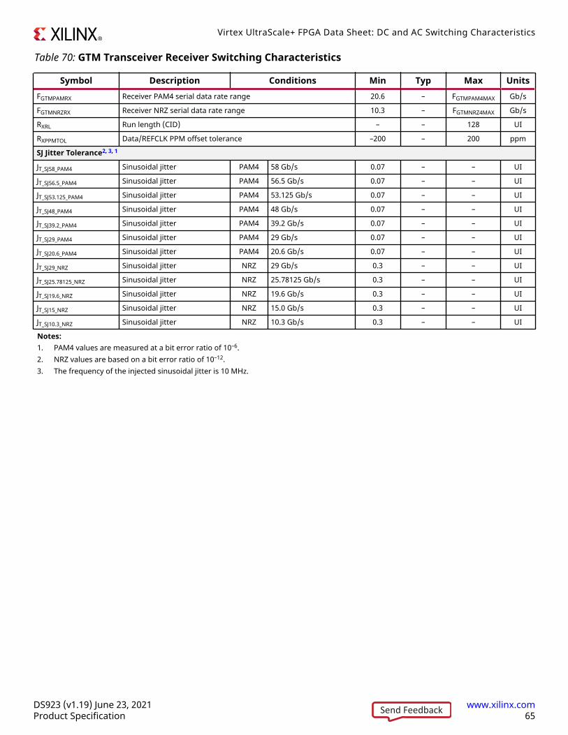
Table 70: GTM Transceiver Receiver Switching Characteristics
Symbol Description Conditions Min Typ Max UnitsFGTMPAMRX Receiver PAM4 serial data rate range 20.6 – FGTMPAM4MAX Gb/s
FGTMNRZRX Receiver NRZ serial data rate range 10.3 – FGTMNRZ4MAX Gb/s
RXRL Run length (CID) – – 128 UI
RXPPMTOL Data/REFCLK PPM offset tolerance –200 – 200 ppm
SJ Jitter Tolerance2, 3, 1
JT_SJ58_PAM4 Sinusoidal jitter PAM4 58 Gb/s 0.07 – – UI
JT_SJ56.5_PAM4 Sinusoidal jitter PAM4 56.5 Gb/s 0.07 – – UI
JT_SJ53.125_PAM4 Sinusoidal jitter PAM4 53.125 Gb/s 0.07 – – UI
JT_SJ48_PAM4 Sinusoidal jitter PAM4 48 Gb/s 0.07 – – UI
JT_SJ39.2_PAM4 Sinusoidal jitter PAM4 39.2 Gb/s 0.07 – – UI
JT_SJ29_PAM4 Sinusoidal jitter PAM4 29 Gb/s 0.07 – – UI
JT_SJ20.6_PAM4 Sinusoidal jitter PAM4 20.6 Gb/s 0.07 – – UI
JT_SJ29_NRZ Sinusoidal jitter NRZ 29 Gb/s 0.3 – – UI
JT_SJ25.78125_NRZ Sinusoidal jitter NRZ 25.78125 Gb/s 0.3 – – UI
JT_SJ19.6_NRZ Sinusoidal jitter NRZ 19.6 Gb/s 0.3 – – UI
JT_SJ15_NRZ Sinusoidal jitter NRZ 15.0 Gb/s 0.3 – – UI
JT_SJ10.3_NRZ Sinusoidal jitter NRZ 10.3 Gb/s 0.3 – – UI
Notes:1. PAM4 values are measured at a bit error ratio of 10–6.2. NRZ values are based on a bit error ratio of 10–12.3. The frequency of the injected sinusoidal jitter is 10 MHz.
Virtex UltraScale+ FPGA Data Sheet: DC and AC Switching Characteristics
DS923 (v1.19) June 23, 2021 www.xilinx.comProduct Specification 65Send Feedback

GTM Transceiver Electrical ComplianceThe Virtex UltraScale+ FPGAs GTM Transceivers User Guide (UG581) contains recommended use modes thatensure compliance for the protocols listed in the following table. The transceiver wizard provides therecommended settings for those use cases and for protocol specific characteristics.
Table 71: GTM Transceiver Protocol List
Protocol Specification Modulation Serial Rate(Gb/s)
ElectricalCompliance
400GAUI-8 IEEE 802.3bs 120D/120E PAM4 53.125 Compliant
200GAUI-4 IEEE 802.3bs 120D/120E PAM4 53.125 Compliant
100GAUI-2 IEEE 802.3cd 135G/135F PAM4 53.125 Compliant
50GAUI-1 IEEE 802.3cd 135G/135F PAM4 53.125 Compliant
200GBASE-KR2 IEEE 802.3cd 137 PAM4 53.125 Compliant
200GBASE-CR2 IEEE 802.3cd 136A PAM4 53.125 Compliant
100GBASE-KR2 IEEE 802.3cd 137 PAM4 53.125 Compliant
100GBASE-CR2 IEEE 802.3cd 136A PAM4 53.125 Compliant
50GBASE-KR IEEE 802.3cd 137 PAM4 53.125 Compliant
50GBASE-CR IEEE 802.3cd 136A PAM4 53.125 Compliant
CAUI-4 IEEE 802.3bm 83D/83E NRZ 25.78125 Compliant
50GAUI-2 IEEE 802.3cd 135D/135E NRZ 26.5625 Compliant
LAUI-2 IEEE 802.3cd 135B/135C NRZ 25.78125 Compliant
25GAUI-1 IEEE 802.3cd 109A/109B NRZ 27.78125 Compliant
100GBASE-KR4 IEEE 802.3bj 93.8 NRZ 25.78125 Compliant
100GBASE-CR4 IEEE 802.3bj 92A NRZ 25.78125 Compliant
25GBASE-KR IEEE 802.3by 111 NRZ 25.78125 Compliant
25GBASE-CR IEEE 802.3by 110 NRZ 25.78125 Compliant
XLPPI IEEE 802.3 86A NRZ 10.3125 Compliant
40GBASE-CR4 IEEE 802.3 85A NRZ 10.3125 Compliant
10GBASE-SR/LR SFF8431 NRZ 10.3125 Compliant
10GBASE-KR IEEE 802.3 72 NRZ 10.3125 Compliant
CEI-56G-VSR/MR/LR-PAM4 Common Electrical (I/O) CEI 4.0 PAM4 39.2-58 Compliant
CEI-25G/28G-VSR/MR/LR Common Electrical (I/O) CEI 4.0 NRZ 19.9-28.1 Compliant
CEI-11G-SR/MR/LR Common Electrical (I/O) CEI 4.0 NRZ 10.3-11.2 Compliant
10G-15G backplane capability 10G NRZ interfaces over backplanes that fall withinthe high-confidence region defined by IEEE 802.3Clause 72
NRZ 15 Compliant
28.21G PAM4 backplanes Insertion loss @ Nyquist (7.05 GHz) at BER < 10e-17
with FECPAM4 28.21 Compliant
58G PAM4 backplanes IEEE 802.3bj style backplanes and copper cables at58 Gb/s (35 dB with RS (544, 514) FEC)
PAM4 58 Compliant
OTU4 optical modules NRZ optical7% FEC
100G OTU4 and OTUCn requirements to CFP2, CFP4,and QSFP28 optics, OIF-CEI28-VSR
NRZ 28.21 Compliant
OTU4 optical module PAM4 optical7% FEC
100G QSFP56, OIF-CEI56-VSR PAM4 56.4 Compliant
Interlaken 25.78125G OIF-CEI-25G-MR @ 20 dB loss NRZ 25.78125 Compliant
Virtex UltraScale+ FPGA Data Sheet: DC and AC Switching Characteristics
DS923 (v1.19) June 23, 2021 www.xilinx.comProduct Specification 66Send Feedback
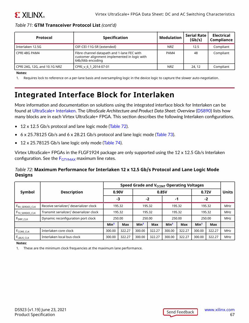
Table 71: GTM Transceiver Protocol List (cont'd)
Protocol Specification Modulation Serial Rate(Gb/s)
ElectricalCompliance
Interlaken 12.5G OIF-CEI-11G-SR (extended) NRZ 12.5 Compliant
CPRI 48G PAM4 Fibre channel datapath and 1-lane FEC withcustomer alignment implemented in logic with64b/66b encoding
PAM4 48 Compliant
CPRI 24G, 12G, and 10.1G NRZ CPRI_v_6_1_2014-07-01 NRZ 24, 12 Compliant
Notes:1. Requires lock to reference on a per-lane basis and oversampling logic in the device logic to capture the slower auto-negotiation.
Integrated Interface Block for InterlakenMore information and documentation on solutions using the integrated interface block for Interlaken can befound at UltraScale+ Interlaken. The UltraScale Architecture and Product Data Sheet: Overview (DS890) lists howmany blocks are in each Virtex UltraScale+ FPGA. This section describes the following Interlaken configurations.
• 12 x 12.5 Gb/s protocol and lane logic mode (Table 72).
• 6 x 25.78125 Gb/s and 6 x 28.21 Gb/s protocol and lane logic mode (Table 73).
• 12 x 25.78125 Gb/s lane logic only mode (Table 74).
Virtex UltraScale+ FPGAs in the FLGF1924 package are only supported using the 12 x 12.5 Gb/s Interlakenconfiguration. See the FGTYMAX maximum line rates.
Table 72: Maximum Performance for Interlaken 12 x 12.5 Gb/s Protocol and Lane Logic ModeDesigns
Symbol DescriptionSpeed Grade and VCCINT Operating Voltages
Units0.90V 0.85V 0.72V-3 -2 -1 -2
FRX_SERDES_CLK Receive serializer/ deserializer clock 195.32 195.32 195.32 195.32 MHz
FTX_SERDES_CLK Transmit serializer/ deserializer clock 195.32 195.32 195.32 195.32 MHz
FDRP_CLK Dynamic reconfiguration port clock 250.00 250.00 250.00 250.00 MHz
Min1 Max Min1 Max Min1 Max Min1 Max
FCORE_CLK Interlaken core clock 300.00 322.27 300.00 322.27 300.00 322.27 300.00 322.27 MHz
FLBUS_CLK Interlaken local bus clock 300.00 322.27 300.00 322.27 300.00 322.27 300.00 322.27 MHz
Notes:1. These are the minimum clock frequencies at the maximum lane performance.
Virtex UltraScale+ FPGA Data Sheet: DC and AC Switching Characteristics
DS923 (v1.19) June 23, 2021 www.xilinx.comProduct Specification 67Send Feedback
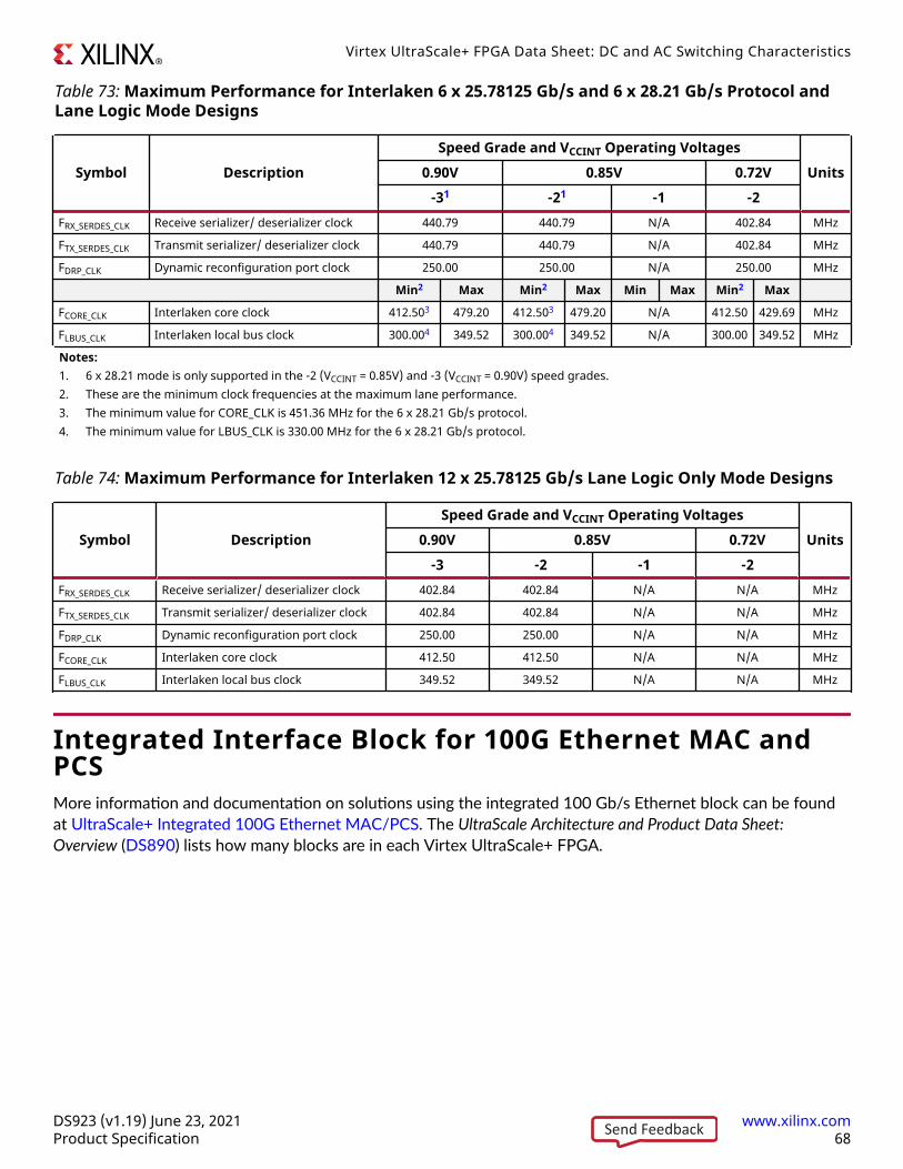
Table 73: Maximum Performance for Interlaken 6 x 25.78125 Gb/s and 6 x 28.21 Gb/s Protocol andLane Logic Mode Designs
Symbol DescriptionSpeed Grade and VCCINT Operating Voltages
Units0.90V 0.85V 0.72V-31 -21 -1 -2
FRX_SERDES_CLK Receive serializer/ deserializer clock 440.79 440.79 N/A 402.84 MHz
FTX_SERDES_CLK Transmit serializer/ deserializer clock 440.79 440.79 N/A 402.84 MHz
FDRP_CLK Dynamic reconfiguration port clock 250.00 250.00 N/A 250.00 MHz
Min2 Max Min2 Max Min Max Min2 Max
FCORE_CLK Interlaken core clock 412.503 479.20 412.503 479.20 N/A 412.50 429.69 MHz
FLBUS_CLK Interlaken local bus clock 300.004 349.52 300.004 349.52 N/A 300.00 349.52 MHz
Notes:1. 6 x 28.21 mode is only supported in the -2 (VCCINT = 0.85V) and -3 (VCCINT = 0.90V) speed grades.2. These are the minimum clock frequencies at the maximum lane performance.3. The minimum value for CORE_CLK is 451.36 MHz for the 6 x 28.21 Gb/s protocol.4. The minimum value for LBUS_CLK is 330.00 MHz for the 6 x 28.21 Gb/s protocol.
Table 74: Maximum Performance for Interlaken 12 x 25.78125 Gb/s Lane Logic Only Mode Designs
Symbol DescriptionSpeed Grade and VCCINT Operating Voltages
Units0.90V 0.85V 0.72V-3 -2 -1 -2
FRX_SERDES_CLK Receive serializer/ deserializer clock 402.84 402.84 N/A N/A MHz
FTX_SERDES_CLK Transmit serializer/ deserializer clock 402.84 402.84 N/A N/A MHz
FDRP_CLK Dynamic reconfiguration port clock 250.00 250.00 N/A N/A MHz
FCORE_CLK Interlaken core clock 412.50 412.50 N/A N/A MHz
FLBUS_CLK Interlaken local bus clock 349.52 349.52 N/A N/A MHz
Integrated Interface Block for 100G Ethernet MAC andPCSMore information and documentation on solutions using the integrated 100 Gb/s Ethernet block can be foundat UltraScale+ Integrated 100G Ethernet MAC/PCS. The UltraScale Architecture and Product Data Sheet:Overview (DS890) lists how many blocks are in each Virtex UltraScale+ FPGA.
Virtex UltraScale+ FPGA Data Sheet: DC and AC Switching Characteristics
DS923 (v1.19) June 23, 2021 www.xilinx.comProduct Specification 68Send Feedback

Table 75: Maximum Performance for 100G Ethernet Designs
Symbol DescriptionSpeed Grade and VCCINT Operating Voltages
Units0.90V 0.85V 0.72V-3 -2 -1 -2
CAUI-10 Mode
FTX_CLK Transmit clock 390.625 390.625 322.266 322.266 MHz
FRX_CLK Receive clock 390.625 390.625 322.266 322.266 MHz
FRX_SERDES_CLK Receive serializer/deserializer clock 390.625 390.625 322.266 322.266 MHz
FDRP_CLK Dynamic reconfiguration port clock 250.00 250.00 250.00 250.00 MHz
CAUI-4, CAUI-4 + RS-FEC, and RS-FEC Transcode Bypass Modes
FTX_CLK Transmit clock 390.625 322.266 322.266 322.266 MHz
FRX_CLK Receive clock 390.625 322.266 322.266 322.266 MHz
FRX_SERDES_CLK Receive serializer/deserializer clock 390.625 322.266 322.266 322.266 MHz
FDRP_CLK Dynamic reconfiguration port clock 250.00 250.00 250.00 250.00 MHz
Integrated Interface Block for PCI Express DesignsMore information and documentation on solutions for PCI Express® designs can be found at PCI Express. TheUltraScale Architecture and Product Data Sheet: Overview (DS890) lists how many blocks are in each VirtexUltraScale+ FPGA. Devices with HBM contain a mixture of PCIE4 and PCIE4C blocks. The PCIE4C blocks areaugmented with support for the CCIX protocol and additional timing enhancements allowing the PCIE4C blocksto run Gen3 x16 when VCCINT = 0.72V.
Table 76: Maximum Performance for PCIE4-based PCI Express Designs
Symbol DescriptionSpeed Grade and VCCINT Operating Voltages
Units0.90V 0.85V 0.72V-3 -2 -1 -2
FPIPECLK Pipe clock maximum frequency 250.00 250.00 250.00 250.00 MHz
FCORECLK Core clock maximum frequency 500.00 500.00 500.00 250.00 MHz
FDRPCLK DRP clock maximum frequency 250.00 250.00 250.00 250.00 MHz
FMCAPCLK MCAP clock maximum frequency 125.00 125.00 125.00 125.00 MHz
Table 77: Maximum Performance for PCIE4C-based PCI Express and CCIX Designs
Symbol DescriptionSpeed Grade and VCCINT Operating Voltages
Units0.90V 0.85V 0.72V-3 -2 -1 -2
FPIPECLK Pipe clock maximum frequency 250.00 250.00 250.00 250.00 MHz
FCORECLK Core clock maximum frequency 500.00 500.00 500.00 500.00 MHz
FCORECLKCCIX CCIX TL interface clock maximum frequency 500.00 500.00 500.00 N/A MHz
FDRPCLK DRP clock maximum frequency 250.00 250.00 250.00 250.00 MHz
FMCAPCLK MCAP clock maximum frequency 125.00 125.00 125.00 125.00 MHz
Virtex UltraScale+ FPGA Data Sheet: DC and AC Switching Characteristics
DS923 (v1.19) June 23, 2021 www.xilinx.comProduct Specification 69Send Feedback

High Bandwidth Memory ControllerThe UltraScale Architecture and Product Data Sheet: Overview (DS890) lists the Virtex UltraScale+ FPGAs withintegrated high-bandwidth memory (HBM).
Table 78: Maximum Performance for High Bandwidth Memory Controller
Symbol DescriptionSpeed Grade and VCCINT Operating Voltages
Units0.90V 0.85V 0.72V-3 -2 -1 -2
FHBM_REF_CLK HBM controller reference clock maximum frequency 450.00 450.00 450.00 450.00 MHz
FACLK AXI interface clock maximum frequency 450.00 450.00 400.00 400.00 MHz
FAPB Advance peripheral bus (APB) clock maximumfrequency
100.00 100.00 100.00 100.00 MHz
FHBM HBM maximum line rate interface to DRAM 1800 1800 1600 1800 Mb/s
System Monitor SpecificationsTable 79: System Monitor Specifications
Parameter Symbol Comments/Conditions Min Typ Max UnitsVCCADC = 1.8V ±3%, VREFP = 1.25V, VREFN = 0V, ADCCLK = 5.2 MHz, Tj = –40°C to 100°C, typical values at Tj = 40°C
ADC Accuracy1
Resolution 10 – – Bits
Integral nonlinearity2 INL – – ±1.5 LSBs
Differential nonlinearity DNL No missing codes, guaranteed monotonic – – ±1 LSBs
Offset error Offset calibration enabled – – ±2 LSBs
Gain error – – ±0.4 %
Sample rate – – 0.2 MS/s
RMS code noise External 1.25V reference – – 1 LSBs
On-chip reference – 1 – LSBs
ADC Accuracy at Extended Temperatures
Resolution Tj = –55°C to 125°C 10 – – Bits
Integral nonlinearity2 INL Tj = –55°C to 125°C – – ±1.5 LSBs
Differential nonlinearity DNL No missing codes, guaranteed monotonicTj = –55°C to 125°C
– – ±1
Analog Inputs2
ADC input ranges Unipolar operation 0 – 1 V
Bipolar operation –0.5 – +0.5 V
Unipolar common mode range (FS input) 0 – +0.5 V
Bipolar common mode range (FS input) +0.5 – +0.6 V
Maximum external channel input ranges Adjacent channels set within these ranges shouldnot corrupt measurements on adjacent channels
–0.1 – VCCADC V
Virtex UltraScale+ FPGA Data Sheet: DC and AC Switching Characteristics
DS923 (v1.19) June 23, 2021 www.xilinx.comProduct Specification 70Send Feedback

Table 79: System Monitor Specifications (cont'd)
Parameter Symbol Comments/Conditions Min Typ Max UnitsOn-Chip Sensor Accuracy
Temperature sensor error1, 3 Tj = –55°C to 125°C (with external REF) – – ±3 °C
Tj = –55°C to 110°C (with internal REF) – – ±3.5 °C
Tj = 110°C to 125°C (with internal REF) – – ±5 °C
Supply sensor error4 Supply voltages 0.72V to 1.2V,Tj = –40°C to 100°C (with external REF)
– – ±0.5 %
Supply voltages 0.72V to 1.2V,Tj = –55°C to 125°C (with external REF)
– – ±1.0 %
All other supply voltages,Tj = –40°C to 100°C (with external REF)
– – ±1.0 %
All other supply voltages,Tj = –55°C to 125°C (with external REF)
– – ±2.0 %
Supply voltages 0.72V to 1.2V,Tj = –40°C to 100°C (with internal REF)
– – ±1.0 %
Supply voltages 0.72V to 1.2V,Tj = –55°C to 125°C (with internal REF)
– – ±2.0 %
All other supply voltages,Tj = –40°C to 100°C (with internal REF)
– – ±1.5 %
All other supply voltages,Tj = –55°C to 125°C (with internal REF)
– – ±2.5 %
Conversion Rate5
Conversion time—continuous tCONV Number of ADCCLK cycles 26 – 32 Cycles
Conversion time—event tCONV Number of ADCCLK cycles – – 21 Cycles
DRP clock frequency DCLK DRP clock frequency 8 – 250 MHz
ADC clock frequency ADCCLK Derived from DCLK 1 – 5.2 MHz
DCLK duty cycle 40 – 60 %
SYSMON Reference6
External reference VREFP Externally supplied reference voltage 1.20 1.25 1.30 V
On-chip reference Ground VREFP pin to AGND, Tj = –40°C to 100°C 1.2375 1.25 1.2625 V
Ground VREFP pin to AGND, Tj = –55°C to 125°C 1.225 1.25 1.275 V
Notes:1. ADC offset errors are removed by enabling the ADC automatic offset calibration feature. The values are specified for when this feature is
enabled.2. See the Analog Input section in the UltraScale Architecture System Monitor User Guide (UG580).3. When reading temperature values directly from the PMBus interface, the SYSMON has a +4°C offset due to the transfer function used by
the PMBus application. For example, the external REF temperature sensor error’s range of ±3°C becomes +1°C to +7°C when thetemperature is read through the PMBus interface.
4. Supply sensor offset and gain errors are removed by enabling the automatic offset and gain calibration feature. The values are specifiedfor when this feature is enabled.
5. See the Adjusting the Acquisition Settling Time section in the UltraScale Architecture System Monitor User Guide (UG580).6. Any variation in the reference voltage from the nominal VREFP = 1.25V and VREFN = 0V will result in a deviation from the ideal transfer
function. This also impacts the accuracy of the internal sensor measurements (i.e., temperature and power supply). However, forexternal ratiometric type applications allowing reference to vary by ±4% is permitted.
Virtex UltraScale+ FPGA Data Sheet: DC and AC Switching Characteristics
DS923 (v1.19) June 23, 2021 www.xilinx.comProduct Specification 71Send Feedback

SYSMON I2C/PMBus InterfacesTable 80: SYSMON I2C Fast Mode Interface Switching Characteristics
Symbol Description1 Min Max UnitsTSMFCKL SCL Low time 1.3 – µs
TSMFCKH SCL High time 0.6 – µs
TSMFCKO SDAO clock-to-out delay – 900 ns
TSMFDCK SDAI setup time 100 – ns
FSMFCLK SCL clock frequency – 400 kHz
Notes:1. The test conditions are configured to the LVCMOS 1.8V I/O standard.
Table 81: SYSMON I2C Standard Mode Interface Switching Characteristics
Symbol Description1 Min Max UnitsTSMSCKL SCL Low time 4.7 – µs
TSMSCKH SCL High time 4.0 – µs
TSMSCKO SDAO clock-to-out delay – 3450 ns
TSMSDCK SDAI setup time 250 – ns
FSMSCLK SCL clock frequency – 100 kHz
Notes:1. The test conditions are configured to the LVCMOS 1.8V I/O standard.
Virtex UltraScale+ FPGA Data Sheet: DC and AC Switching Characteristics
DS923 (v1.19) June 23, 2021 www.xilinx.comProduct Specification 72Send Feedback

Configuration Switching Characteristics
Table 82: Configuration Switching Characteristics
Symbol DescriptionSpeed Grade and VCCINT Operating Voltages
Units0.90V 0.85V 0.72V-3 -2 -1 -2
Power-up Timing Characteristics
TPL Program latency for XCVU19P 12 12 12 12 ms, Max
Program latency for all other devices 8.5 8.5 8.5 8.5 ms, Max
TPOR Power-on reset (40 ms maximum ramp rate) 65 65 65 65 ms, Max
0 0 0 0 ms, Min
Power-on reset with POR override (2 msmaximum ramp rate)
15 15 15 15 ms, Max
5 5 5 5 ms, Min
TPROGRAM Program pulse width 250 250 250 250 ns, Min
CCLK Output (Master Mode)
TICCK Master CCLK output delay from INIT_B 150 150 150 150 ns, Min
TMCCKL1 Master CCLK clock Low time duty cycle 40/60 40/60 40/60 40/60 %, Min/Max
TMCCKH Master CCLK clock High time duty cycle 40/60 40/60 40/60 40/60 %, Min/Max
FMCCK Master SPI (x1/x2/x4) CCLK frequency 125 125 125 100 MHz, Max
Master SPI (x8) orMaster BPI (x8/x16)2
CCLK frequency
XCVU3P, XQVU3P,XCVU5P, XCVU7P,XQVU7P, XCVU9P
125 125 125 100 MHz, Max
XCVU11P, XQVU11P,XCVU13P,XCVU19P,XCVU27P,XCVU29P, XCVU31P,XCVU33P, XCVU35P,XCVU37P, XCVU45P,XCVU47P, XCVU57P
125 125 125 60 MHz, Max
XCVU23P 100 100 100 60 MHz, Max
FMCCK_START Master CCLK frequency at start ofconfiguration
2.7 2.7 2.7 2.7 MHz, Typ
FMCCKTOL Frequency tolerance, master mode withrespect to nominal CCLK
±15 ±15 ±15 ±15 %, Max
CCLK Input (Slave Mode)
TSCCKL Slave CCLK clock minimum Low time 2.5 2.5 2.5 2.5 ns, Min
TSCCKH Slave CCLK clock minimum High time 2.5 2.5 2.5 2.5 ns, Min
Virtex UltraScale+ FPGA Data Sheet: DC and AC Switching Characteristics
DS923 (v1.19) June 23, 2021 www.xilinx.comProduct Specification 73Send Feedback

Table 82: Configuration Switching Characteristics (cont'd)
Symbol DescriptionSpeed Grade and VCCINT Operating Voltages
Units0.90V 0.85V 0.72V-3 -2 -1 -2
FSCCK Slave Serial/Slave SelectMAPCCLK frequency
XCVU3P, XQVU3P,XCVU5P, XCVU7P,XQVU7P, XCVU9P
125 125 125 100 MHz, Max
Slave Serial CCLKfrequency
XCVU11P, XQVU11P,XCVU13P, XCVU19P,XCVU27P, XCVU29P,XCVU31P, XCVU33P,XCVU35P, XCVU37P,XCVU45P, XCVU47P,XCVU57P
125 125 125 100 MHz, Max
XCVU23P 125 125 125 100 MHz, Max
Slave SelectMAP CCLKfrequency
XCVU11P, XQVU11P,XCVU13P, XCVU19P,XCVU27P, XCVU29P,XCVU31P, XCVU33P,XCVU35P, XCVU37P,XCVU45P, XCVU47P,XCVU57P
125 125 125 60 MHz, Max
XCVU23P 100 100 100 60 MHz, Max
EMCCLK Input (Master Mode)
TEMCCKL External master CCLK Low time 2.5 2.5 2.5 2.5 ns, Min
TEMCCKH External master CCLK High time 2.5 2.5 2.5 2.5 ns, Min
FEMCCK External master CCLK frequency with SPIx1/x2/x4
125 125 125 100 MHz, Max
External master CCLKfrequencywith SPI x8 orBPI x8/x162
XCVU3P, XQVU3P,XCVU5P, XCVU7P,XQVU7P, XCVU9P
125 125 125 100 MHz, Max
XCVU11P, XQVU11P,XCVU13P, XCVU19P,XCVU27P, XCVU29P,XCVU31P, XCVU33P,XCVU35P, XCVU37P,XCVU45P, XCVU47P,XCVU57P
125 125 125 60 MHz, Max
XCVU23P 100 100 100 60 MHz, Max
Virtex UltraScale+ FPGA Data Sheet: DC and AC Switching Characteristics
DS923 (v1.19) June 23, 2021 www.xilinx.comProduct Specification 74Send Feedback

Table 82: Configuration Switching Characteristics (cont'd)
Symbol DescriptionSpeed Grade and VCCINT Operating Voltages
Units0.90V 0.85V 0.72V-3 -2 -1 -2
Internal Configuration Access Port
FICAPCK Internal configurationaccess port (ICAPE3)
XCVU3P, XQVU3P,XCVU23P
200 200 200 150 MHz, Max
Master SLR ICAPE3accessing entire device
XCVU5P, XCVU7P,XQVU7P, XCVU9P,XCVU11P, XQVU11P,XCVU13P, XCVU19P,XCVU27P, XCVU29P,XCVU31P, XCVU33P,XCVU35P, XCVU37P,XCVU45P, XCVU47P,XCVU57P
125 125 125 125 MHz, Max
SLR ICAPE3 accessinglocal SLR
XCVU5P, XCVU7P,XQVU7P, XCVU9P,XCVU11P, XQVU11P,XCVU13P, XCVU19P,XCVU27P, XCVU29P,XCVU31P, XCVU33P,XCVU35P, XCVU37P,XCVU45P, XCVU47P,XCVU57P
200 200 200 150 MHz, Max
Slave Serial Mode Programming Switching
TDCCK/TCCKD DIN setup/hold 3.0/0 3.0/0 3.0/0 4.0/0 ns, Min
TCCO DOUT clock to out 8.0 8.0 8.0 9.0 ns, Max
SelectMAP Mode Programming Switching
TSMDCCK/TSMCCKD D[31:00] setup/hold XCVU3P, XQVU3P,XCVU5P, XCVU7P,XQVU7P, XCVU9P
4.0/0 4.0/0 4.0/0 5.0/0 ns, Min
XCVU11P, XQVU11P,XCVU13P, XCVU19P,XCVU27P, XCVU29P,XCVU31P, XCVU33P,XCVU35P, XCVU37P,XCVU45P, XCVU47P,XCVU57P
4.5/0 4.5/0 4.5/0 8.0/0 ns, Min
XCVU23P 5.5/0 5.5/0 5.5/0 8.5/0 ns, Min
TSMCSCCK/TSMCCKCS CSI_B setup/hold XCVU3P, XQVU3P,XCVU5P, XCVU7P,XQVU7P, XCVU9P
4.0/0 4.0/0 4.0/0 5.0/0 ns, Min
XCVU11P, XQVU11P,XCVU13P, XCVU19P,XCVU27P, XCVU29P,XCVU31P, XCVU33P,XCVU35P, XCVU37P,XCVU45P, XCVU47P,XCVU57P
4.5/0 4.5/0 4.5/0 7.5/0 ns, Min
XCVU23P 5.0/0 5.0/0 5.0/0 8.5/0 ns, Min
Virtex UltraScale+ FPGA Data Sheet: DC and AC Switching Characteristics
DS923 (v1.19) June 23, 2021 www.xilinx.comProduct Specification 75Send Feedback

Table 82: Configuration Switching Characteristics (cont'd)
Symbol DescriptionSpeed Grade and VCCINT Operating Voltages
Units0.90V 0.85V 0.72V-3 -2 -1 -2
TSMWCCK/TSMCCKW RDWR_B setup/hold XCVU3P, XQVU3P,XCVU5P, XCVU7P,XQVU7P, XCVU9P
10.0/0 10.0/0 10.0/0 11.0/0 ns, Min
XCVU11P, XQVU11P,XCVU13P, XCVU19P,XCVU27P, XCVU29P,XCVU31P, XCVU33P,XCVU35P, XCVU37P,XCVU45P, XCVU47P,XCVU57P
11.0/0 11.0/0 11.0/0 17.0/0 ns, Min
XCVU23P 11.0/0 11.0/0 17.5/0 17.5/0 ns, Min
TSMCKCSO CSO_B clock to out(330Ω pull-up resistorrequired)
XCVU3P, XQVU3P,XCVU5P, XCVU7P,XQVU7P, XCVU9P
7.0 7.0 7.0 7.0 ns, Max
XCVU11P, XQVU11P,XCVU13P, XCVU19P,XCVU27P, XCVU29P,XCVU31P, XCVU33P,XCVU35P, XCVU37P,XCVU45P, XCVU47P,XCVU57P
7.0 7.0 7.0 10.0 ns, Max
XCVU23P 7.0 7.0 7.0 10.0 ns, Max
TSMCO D[31:00] clock to out inreadback
XCVU3P, XQVU3P,XCVU5P, XCVU7P,XQVU7P, XCVU9P
8.0 8.0 8.0 8.0 ns, Max
XCVU11P, XQVU11P,XCVU13P, XCVU19P,XCVU27P, XCVU29P,XCVU31P, XCVU33P,XCVU35P, XCVU37P,XCVU45P, XCVU47P,XCVU57P
8.0 8.0 8.0 10.0 ns, Max
XCVU23P 8.0 8.0 8.0 10.0 ns, Max
FRBCCK Readback frequency XCVU3P, XQVU3P,XCVU5P, XCVU7P,XQVU7P, XCVU9P
125 125 125 100 MHz, Max
XCVU11P, XQVU11P,XCVU13P, XCVU19P,XCVU27P, XCVU29P,XCVU31P, XCVU33P,XCVU35P, XCVU37P,XCVU45P, XCVU47P,XCVU57P
125 125 125 60 MHz, Max
XCVU23P 100 100 100 60 ns, Max
Boundary-Scan Port Timing Specifications
TTAPTCK/TTCKTAP TMS and TDI setup/hold
XCVU3P, XQVU3P,XCVU23P
3.0/2.0 3.0/2.0 3.0/2.0 3.0/2.0 ns, Min
XCVU5P, XCVU7P,XQVU7P, XCVU9P,XCVU11P, XQVU11P,XCVU13P, XCVU19P,XCVU27P, XCVU29P,XCVU31P, XCVU33P,XCVU35P, XCVU37P,XCVU45P, XCVU47P,XCVU57P
8.5/2.0 8.5/2.0 8.5/2.0 8.5/2.0 ns, Min
Virtex UltraScale+ FPGA Data Sheet: DC and AC Switching Characteristics
DS923 (v1.19) June 23, 2021 www.xilinx.comProduct Specification 76Send Feedback

Table 82: Configuration Switching Characteristics (cont'd)
Symbol DescriptionSpeed Grade and VCCINT Operating Voltages
Units0.90V 0.85V 0.72V-3 -2 -1 -2
TTCKTDO TCK falling edge toTDO output
XCVU3P, XQVU3P,XCVU23P
7.0 7.0 7.0 7.0 ns, Max
XCVU5P, XCVU7P,XQVU7P, XCVU9P,XCVU11P, XQVU11P,XCVU13P, XCVU19P,XCVU27P, XCVU29P,XCVU31P, XCVU33P,XCVU35P, XCVU37P,XCVU45P, XCVU47P,XCVU57P
15.0 15.0 15.0 15.0 ns, Max
FTCK TCK frequency XCVU3P, XQVU3P 66 66 66 66 MHz, Max
XCVU5P, XCVU7P,XQVU7P, XCVU9P,XCVU11P, XQVU11P,XCVU13P, XCVU19P,XCVU27P, XCVU29P,XCVU31P, XCVU33P,XCVU35P, XCVU37P,XCVU45P, XCVU47P,XCVU57P
20 20 20 20 MHz, Max
XCVU23P 66 66 66 50 MHz, Max
BPI Master Flash Mode Programming Switching
TBPICCO A[28:00], RS[1:0], FCS_B, FOE_B, FWE_B, ADV_Bclock to out
10 10 10 10 ns, Max
TBPIDCC/TBPICCD D[15:00] setup/hold XCVU3P, XQVU3P,XCVU5P, XCVU7P,XQVU7P, XCVU9P
4.0/0 4.0/0 4.0/0 5.0/0 ns, Min
XCVU11P, XQVU11P,XCVU13P, XCVU19P,XCVU27P, XCVU29P,XCVU31P, XCVU33P,XCVU35P, XCVU37P,XCVU45P, XCVU47P,XCVU57P
4.5/0 4.5/0 4.5/0 8.0/0 ns, Min
XCVU23P 5.5/0 5.5/0 5.5/0 8.5/0 ns, Min
SPI Master Flash Mode Programming Switching
TSPIDCC/TSPICCD D[03:00] setup/hold 3.0/0 3.0/0 3.0/0 4.0/0 ns, Min
TSPIDCC/TSPICCD D[07:04] setup/hold XCVU3P, XQVU3P,XCVU5P, XCVU7P,XQVU7P, XCVU9P
4.0/0 4.0/0 4.0/0 5.0/0 ns, Min
XCVU11P, XQVU11P,XCVU13P, XCVU19P,XCVU27P, XCVU29P,XCVU31P, XCVU33P,XCVU35P, XCVU37P,XCVU45P, XCVU47P,XCVU57P
4.5/0 4.5/0 4.5/0 8.0/0 ns, Min
XCVU23P 5.5/0 5.5/0 5.5/0 8.5/0 ns, Min
TSPICCM MOSI clock to out 8.0 8.0 8.0 8.0 ns, Max
TSPICCM2 D[04] clock to out 10.0 10.0 10.0 10.0 ns, Max
TSPICCFC FCS_B clock to out 8.0 8.0 8.0 8.0 ns, Max
TSPICCFC2 FCS2_B clock to out 10.0 10.0 10.0 10.0 ns, Max
Virtex UltraScale+ FPGA Data Sheet: DC and AC Switching Characteristics
DS923 (v1.19) June 23, 2021 www.xilinx.comProduct Specification 77Send Feedback
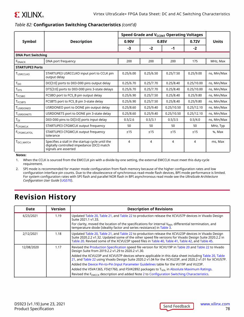
Table 82: Configuration Switching Characteristics (cont'd)
Symbol DescriptionSpeed Grade and VCCINT Operating Voltages
Units0.90V 0.85V 0.72V-3 -2 -1 -2
DNA Port Switching
FDNACK DNA port frequency 200 200 200 175 MHz, Max
STARTUPE3 Ports
TUSRCCLKO STARTUPE3 USRCCLKO input port to CCLK pinoutput delay
0.25/6.00 0.25/6.50 0.25/7.50 0.25/9.00 ns, Min/Max
TDO DO[3:0] ports to D03-D00 pins output delay 0.25/6.70 0.25/7.70 0.25/8.40 0.25/10.00 ns, Min/Max
TDTS DTS[3:0] ports to D03-D00 pins 3-state delays 0.25/6.70 0.25/7.70 0.25/8.40 0.25/10.00 ns, Min/Max
TFCSBO FCSBO port to FCS_B pin output delay 0.25/6.90 0.25/7.50 0.25/8.40 0.25/9.80 ns, Min/Max
TFCSBTS FCSBTS port to FCS_B pin 3-state delay 0.25/6.90 0.25/7.50 0.25/8.40 0.25/9.80 ns, Min/Max
TUSRDONEO USRDONEO port to DONE pin output delay 0.25/8.60 0.25/9.40 0.25/10.50 0.25/12.10 ns, Min/Max
TUSRDONETS USRDONETS port to DONE pin 3-state delay 0.25/8.60 0.25/9.40 0.25/10.50 0.25/12.10 ns, Min/Max
TDI D03-D00 pins to DI[3:0] ports input delay 0.5/2.6 0.5/3.1 0.5/3.5 0.5/4.0 ns, Min/Max
FCFGMCLK STARTUPE3 CFGMCLK output frequency 50 50 50 50 MHz, Typ
FCFGMCLKTOL STARTUPE3 CFGMCLK output frequencytolerance
±15 ±15 ±15 ±15 %, Max
TDCI_MATCH Specifies a stall in the startup cycle until thedigitally controlled impedance (DCI) matchsignals are asserted
4 4 4 4 ms, Max
Notes:1. When the CCLK is sourced from the EMCCLK pin with a divide-by-one setting, the external EMCCLK must meet this duty-cycle
requirement.2. SPI mode is recommended for master mode configuration from flash memory because of the higher configuration rates and low
configuration interface pin counts. Due to the obsolescence of synchronous read-mode flash devices, BPI mode performance is limited.For system configuration rates with SPI flash and parallel NOR flash in BPI asynchronous read mode see the UltraScale ArchitectureConfiguration User Guide (UG570).
Revision HistoryDate Version Description of Revisions
6/23/2021 1.19 Updated Table 20, Table 21, and Table 22 to production release the XCVU57P devices in Vivado DesignSuite 2021.1 v1.33.For clarity, moved the location of the specifications for internal VREF, differential termination, andtemperature diode (ideality factor and series resistance) in Table 3.
2/12/2021 1.18 Updated Table 20, Table 21, and Table 22 to production release the XCVU23P devices in Vivado DesignSuite 2020.2.2 v1.32. Updated some of the other speed file versions for Vivado Design Suite 2020.2.2 in Table 20. Revised some of the XCVU23P speed files in Table 40, Table 41, Table 42, and Table 45.
12/08/2020 1.17 Revised the Production Specification speed file version for XCVU19P in Table 20 and Table 22 to VivadoDesign Suite from 2019.2.2 v1.29 to 2020.2 v1.30.Added the XCVU23P and XCVU57P devices where applicable in this data sheet including Table 20, Table21, and Table 22 using Vivado Design Suite 2020.2 v1.04 for the XCVU23P, and 2020.2 v1.01 for XCVU57P.Added the Device Pin-to-Pin Input Parameter Guidelines table for the VU19P and VU23P.Added the VSVA1365, FSVJ1760, and FSVK2892 packages to TSOL in Absolute Maximum Ratings.Revised the FEMCCK description and added Note 2 to Configuration Switching Characteristics.
Virtex UltraScale+ FPGA Data Sheet: DC and AC Switching Characteristics
DS923 (v1.19) June 23, 2021 www.xilinx.comProduct Specification 78Send Feedback

Date Version Description of Revisions8/20/2020 1.16 Added the XCVU23P and XCVU57P devices throughout.
Revised the production software and speed specification release version for the XCVU27P -3E(VCCINT = 0.90V) and the XCVU29P -3E (VCCINT = 0.90V) using Vivado Design Suite 2020.1.1 v1.30 in Table22.Updated Table 20, Table 21, and Table 22 to production release the XCVU19P device in -2E (VCCINT = 0.85V)and -1E (VCCINT = 0.85V) speed/voltage grades and all packages using Vivado Design Suite 2019.2.2 v1.29.
3/13/2020 1.15 Updated the power-on current values for XCVU19P in Table 7.In Table 63, updated Note 2.Added the program latency (TPL) for the XCVU19P to Table 82.
11/25/2019 1.14 Updated Table 20, Table 21, and Table 22 to production release:XCVU27P and XCVU29P devices in -3E, -2LE (VCCINT = 0.85V), and -2LE (VCCINT = 0.72V) speed/voltagegrades and all packages using Vivado Design Suite 2019.2 v1.28
9/30/2019 1.13 Updated Table 20, Table 21, and Table 22 to production release:XCVU27P and XCVU29P devices in -1E, -1I, -2E and -2I speed/voltage grades and all packages usingVivado Design Suite 2019.1.3 v1.27XCVU47P and XCVU49P devices in -3E, -2E, -2LE, -1E (VCCINT = 0.85V) and -2LE (VCCINT = 0.72V)) usingVivado Design Suite 2019.1 v1.25
Deleted GTM transceiver support for DC coupled operation in Table 61. Updated PAM4 and NRZspecifications in Table 61, Table 63, Table 69, and Table 70. Updated the specifications in Table 67. In Table 69, deleted support for TX lane-to-lane skew and TX phase alignment. Removed the GTMTransceiver Clock Output Level Specification table. Revised the GTM Transceiver Electrical Compliancetable.
8/21/2019 1.12 Added the XCVU19P device in the FSVA3824 and FSVB3824 packages where applicable.Increased the maximum line rate of the QPLL0 -1 (VCCINT = 0.85V) output divider 1 in Table 52 andupdated Notes 4 and 5.Revised Table 63: GTM Transceiver Performance and the GTM Transceiver Electrical Compliance table.
7/19/2019 1.11 Updated Table 20, Table 21, and Table 22 to add the XCVU45P and XCVU47P devices, updated all speedfile versions to Vivado Design Suite 2019.1.1 v1.26, and production release the XCVU31P, XCVU33P,XCVU35P, and XCVU37P devices in the -3 (VCCINT = 0.90V) speed/voltage grade in Vivado Design Suite2019.1 v1.25.Added the maximum reflow soldering temperature (TSOL) values for the FFRC1517, FFRA2104, FFRB2104,and FFRC2104 packages in Table 1.Updated Note 4 in Table 3.Updated the GTM sequence in Power-On/Off Power Supply Sequencing.
4/26/2019 1.10 Updated Table 20, Table 21, and Table 22 to production release the following devices in the VivadoDesign Suite.
XCVU31P: 2018.3.1 v1.24 (-2E, -2LE, -1E (VCCINT = 0.85V) and -2LE (VCCINT = 0.72V))XCVU33P: 2018.3.1 v1.24 (-2E, -2LE, -1E (VCCINT = 0.85V) and -2LE (VCCINT = 0.72V))XCVU37P: 2018.3.1 v1.24 (-2E, -2LE, -1E (VCCINT = 0.85V) and -2LE (VCCINT = 0.72V))XCVU39P: 2018.3.1 v1.24 (-2E, -2LE, -1E (VCCINT = 0.85V) and -2LE (VCCINT = 0.72V))XQVU3P: 2018.3 v1.23XQVU7P: 2018.3.1 v1.23XQVU11P: 2018.3.1 v1.23
In Table 1, revised the TSTG.Added Note 14 in Table 2.Updated the VU3xP values in Table 7.Added LVDS component mode notes to FPGA Logic Performance Characteristics.
1/04/2019 1.9 Added the XCVU27P and XCVU29P devices. Also added the GTM Transceiver Specifications.Updated the calculations in Table 7: Power-on Current by DeviceUpdated the speed specification version by device for Table 20 to Vivado Design Suite 2018.3.Updated the VIDIFF description in Table 19.In Table 57, updated Note 2.Removed PCI Express Gen4 support in Table 76: Maximum Performance for PCIE4-based PCI ExpressDesigns and Notes 1, Note 2, and Note 3. In Table 77: Maximum Performance for PCIE4C-based PCIExpress and CCIX Designs, removed Notes 1, 2, 3, 4, and 5.
Virtex UltraScale+ FPGA Data Sheet: DC and AC Switching Characteristics
DS923 (v1.19) June 23, 2021 www.xilinx.comProduct Specification 79Send Feedback
Date Version Description of Revisions8/01/2018 1.8 Added XCVU3xP data to Table 6.
Updated the speed specification version by device for Table 20 to Vivado Design Suite 2018.2.1.In Table 24, added Note 4 to the LVDS RX DDR maximum data.In Table 75, revised the calculated values from 322.223 to 322.266.
6/18/2018 1.7 Revised the speed grade -1 (VCCINT = 0.85) FGTYMAX in Table 52, which also revised values in Table 57 andadded Note 2.Revised FACLK and added FHBM to Table 78.
4/09/2018 1.6 Added the XCVU31P, XCVU33P, XCVU35P, and XCVU37P devices throughout the data sheet. Added thespecifications for High Bandwidth Memory to Table 1, Table 2, Table 6, the Power-On/Off Power SupplySequencing section, Table 7, Table 8, and Table 78.Updated Table 20, Table 21, and Table 22 to production release the following devices in Vivado DesignSuite 2018.1 v1.19.XCVU3P: -3E (VCCINT = 0.90V)XCVU5P: -3E (VCCINT = 0.90V)XCVU7P: -3E (VCCINT = 0.90V)XCVU9P: -3E (VCCINT = 0.90V)Added Table 43 and Table 47. Added Note 2 and Note 3 to Table 46. Revised Table 75 to add specifc modespecifications and remove Note 1. Added Table 77.
2/07/2018 1.5 Updated Table 20, Table 21, and Table 22 to production release the following devices in Vivado DesignSuite 2017.4.1 v1.18.XCVU11P: -3E (VCCINT = 0.90V)XCVU13P: -3E (VCCINT = 0.90V)Revised some of the -3E (VCCINT = 0.90V) speed files in Table 40, Table 41, Table 42, and Table 45.Revised the DVPPOUT control signal in Table 49.
11/28/2017 1.4 In Table 1, corrected the minimum voltage for the System Monitor section.Updated Table 20, Table 21, and Table 22 to production release all the -2LE (VCCINT = 0.85V) and -2LE(VCCINT = 0.72V) devices/speed/temperature grades in Vivado Design Suite 2017.3.1.Revised the FREFCLK descriptions in Table 35.Revised some of the -3E and -2LE (VCCINT = 0.72V) speed files in Table 40, Table 41, Table 42, Table 45, andadded package values to Table 48.Revised the FGTYQRANGE2 -1 speed grade minimum in Table 52. Added TSPICCM2 and TSPICCFC2 to Table 82.
10/02/2017 1.3 Updated Table 1 to include maximum TSOLUpdated Table 20, Table 21, and for dry rework and reflow soldering.Table 22 to production release thefollowing devices/speed/temperature grades in Vivado Design Suite 2017.2.1.XCVU11P: -2E, -2I, -1E, -1IXCVU13P: -2E, -2I, -1E, -1IIn Table 29, revised the TOUTBUF_DELAY_O_PAD -2 (VCCINT for dry r = 0.85V) values for DIFF_SSTL135_S,DIFF_SSTL15_DCI_S, DIFF_SSTL15_S, DIFF_SSTL18_I_DCI_S, and DIFF_SSTL18_I_S.Revised some of the -3E and -2LE (VCCINT = 0.72V) speed files in Table 29, Table 40, Table 41, and Table 42.
6/27/2017 1.2 Updated Table 20, Table 21, and Table 22 to production release the following devices/speed/temperaturegrades in Vivado Design Suite 2017.2.XCVU5P: -2E, -2I, -1E, -1IXCVU7P: -2E, -2I, -1E, -1IXCVU9P: -2E, -2I, -1E, -1IUpdated Note 12 in Table 2 for clarity. In Table 3, removed unsupported voltages (2.5V and 3.3V) fromIRPU and IRPD. Added Note 3 to Table 27. Revised the -3E and -2LE (VCCINT = 0.72V) speed files in Table 29, Table 30, Table 40, Table 41, Table 42, and Table 45. In Table 31 removed from the input delaymeasurement methodology section the following class II I/O standards: SSTL135_II, SSTL15_II, SSTL18_II,DIFF_SSTL135_II, DIFF_SSTL15_II and DIFF_SSTL18_II. Updated the FMAX symbol names and values in Table34. Added Note 1 to Table 36. Added Note 3 to Table 76. In Table 82, updated the -2LE (VCCINT = 0.72V)specifications for FMCCK, FSCCK, FEMCCK, FICAPCK, TSMDCCK/TSMCCKD, TSMCKCSO, TSMCO, FRBCCK, TBPIDCC/TBPICCD,and TSPIDCC/TSPICCD.
Virtex UltraScale+ FPGA Data Sheet: DC and AC Switching Characteristics
DS923 (v1.19) June 23, 2021 www.xilinx.comProduct Specification 80Send Feedback

Date Version Description of Revisions4/19/2017 1.1 Updated the Summary description. In Table 1, updated Note 6, added data, and added Note 7, Note 8,
and Note 9. Updated and added data to Table 2 through Table 7.Removed the -1LI speed grade.Updated Table 20, Table 21, and Table 22 to production release in Vivado Design Suite 2017.1 for theXCVU3P: -2E, -2I, -1E, -1I.Updated Table 19. Added Note 1 to Table 21. Updated Table 23, Table 24, Table 29, Table 30, Table 31, Table 33, Table 34, and Table 35. Added Table 25. Added MMCM_FDPRCLK_MAX to Table 38 andPLL_FDPRCLK_MAX to Table 39. Updated to Vivado Design Suite 2017.1 Table 40, Table 41, Table 42, and Table 45. Added data to Table 46 and Table 48. Updated the GTY Transceiver Specifications section.Revised the Integrated Interface Block for Interlaken section. Updated the System Monitor Specificationssection adding notes to the tables. Updated the Configuration Switching Characteristics section.Removed the eFUSE Programming Conditions table and added the specifications to Table 2 and Table 3.Updated the Automotive Applications Disclaimer.
4/20/2016 1.0 Initial Xilinx release.
Please Read: Important Legal NoticesThe information disclosed to you hereunder (the "Materials") is provided solely for the selection and use ofXilinx products. To the maximum extent permitted by applicable law: (1) Materials are made available "AS IS" andwith all faults, Xilinx hereby DISCLAIMS ALL WARRANTIES AND CONDITIONS, EXPRESS, IMPLIED, ORSTATUTORY, INCLUDING BUT NOT LIMITED TO WARRANTIES OF MERCHANTABILITY, NON-INFRINGEMENT, OR FITNESS FOR ANY PARTICULAR PURPOSE; and (2) Xilinx shall not be liable (whether incontract or tort, including negligence, or under any other theory of liability) for any loss or damage of any kindor nature related to, arising under, or in connection with, the Materials (including your use of the Materials),including for any direct, indirect, special, incidental, or consequential loss or damage (including loss of data,profits, goodwill, or any type of loss or damage suffered as a result of any action brought by a third party) even ifsuch damage or loss was reasonably foreseeable or Xilinx had been advised of the possibility of the same. Xilinxassumes no obligation to correct any errors contained in the Materials or to notify you of updates to theMaterials or to product specifications. You may not reproduce, modify, distribute, or publicly display theMaterials without prior written consent. Certain products are subject to the terms and conditions of Xilinx'slimited warranty, please refer to Xilinx's Terms of Sale which can be viewed at https://www.xilinx.com/legal.htm#tos; IP cores may be subject to warranty and support terms contained in a license issued to you byXilinx. Xilinx products are not designed or intended to be fail-safe or for use in any application requiring fail-safeperformance; you assume sole risk and liability for use of Xilinx products in such critical applications, pleaserefer to Xilinx's Terms of Sale which can be viewed at https://www.xilinx.com/legal.htm#tos.
AUTOMOTIVE APPLICATIONS DISCLAIMER
AUTOMOTIVE PRODUCTS (IDENTIFIED AS "XA" IN THE PART NUMBER) ARE NOT WARRANTED FOR USEIN THE DEPLOYMENT OF AIRBAGS OR FOR USE IN APPLICATIONS THAT AFFECT CONTROL OF AVEHICLE ("SAFETY APPLICATION") UNLESS THERE IS A SAFETY CONCEPT OR REDUNDANCY FEATURECONSISTENT WITH THE ISO 26262 AUTOMOTIVE SAFETY STANDARD ("SAFETY DESIGN"). CUSTOMERSHALL, PRIOR TO USING OR DISTRIBUTING ANY SYSTEMS THAT INCORPORATE PRODUCTS,THOROUGHLY TEST SUCH SYSTEMS FOR SAFETY PURPOSES. USE OF PRODUCTS IN A SAFETYAPPLICATION WITHOUT A SAFETY DESIGN IS FULLY AT THE RISK OF CUSTOMER, SUBJECT ONLY TOAPPLICABLE LAWS AND REGULATIONS GOVERNING LIMITATIONS ON PRODUCT LIABILITY.
Virtex UltraScale+ FPGA Data Sheet: DC and AC Switching Characteristics
DS923 (v1.19) June 23, 2021 www.xilinx.comProduct Specification 81Send Feedback