CV763A / CV763B - Hacom B manual.pdf · CV763A / CV763B 400MHz FSB / VGA ... Advanced IR port also...
67
CV763A / CV763B 400MHz FSB / VGA /Multi-LANs / Sound / PCMCIA / Mini PCI / PCI NO.CV763A / CV763B 400MHz FSB . All-in-one Sound . 4 LAN ports SATA 150 . ATA 66/100/133 . USB . IrDA . CF 12V DC-IN 7 APR . 26 . 2007
Transcript of CV763A / CV763B - Hacom B manual.pdf · CV763A / CV763B 400MHz FSB / VGA ... Advanced IR port also...
CV763A / CV763B
400MHz FSB / VGA /Multi-LANs / Sound / PCMCIA / Mini PCI / PCI
NO.CV763A / CV763B
400MHz FSB . All-in-one
Sound . 4 LAN ports
SATA 150 . ATA 66/100/133 . USB . IrDA . CF
12V DC-IN
7
APR . 26 . 2007

i
CV763A / CV763BWarning!........................................................................................................................... 1Hardware Notice Guide ............................................................................................. 2CHAPTER 1 GENERAL INFORMATION ........................................................................ 41-1 MAJOR FEATURE........................................................................................................ 51-2 SPECIFICATION .......................................................................................................... 61-3 INSTALLING THE MINI PCI CARD..............................................................................1-3-1 REMOVING THE MINI PCI CARD.............................................................................1-4 PACKING LIST*............................................................................................................CHAPTER 2 HARDWARE INSTALLATION ................................................................... 2-1 UNPACKING PRECAUTION ....................................................................................... 2-2 UNPACKING CHECKUP ............................................................................................. 2-3 DIMENSION ................................................................................................................ 2-4 LAYOUT ...................................................................................................................... 2-5 DIAGRAM ...................................................................................................................2-5-1 DIAGRAM (CV763B)................................................................................................2-5-2 BOTTOM SIDE DIAGRAM / BACK PANEL..............................................................2-6 INSTALL MEMORY .................................................................................................... 2-7 LIST OF JUMPERS .................................................................................................... 2-8 JUMPER SETTING DESCRIPTION .......................................................................... 2-9 CMOS DATA SET ....................................................................................................... 2-10 JCF2 CF CARD POWER VOLTAGE SELECT ......................................................... 2-11 JCF1 CF CARD MASTER/ SLAVE SELECT ...........................................................CHAPTER 3 CONNECTION ........................................................................................ 233-1 LIST OF CONNECTORS............................................................................................ 3-2 FAN CONNECTOR ..................................................................................................... 3-3 IDE CONNECTORS ................................................................................................... 3-4 COMPACT-FLASH MEMORY SOCKET .................................................................... 263-5 SERIAL PORT CONNECTOR / VGA CONNECTOR.................................................. 3-6 EXTERNAL KEYBOARD AND MOUSE CONNECTOR ........................................... 3-7 USB PORT / HEADER ............................................................................................... 293-8 LAN PORT .................................................................................................................3-9 AUDIO PORT CONNECTOR .....................................................................................3-10 WDT/DIO FUNCTION PORT ...................................................................................3-11 WDT/DIO SAMPLE CODE .......................................................................................3-12 IR CONNECTOR .....................................................................................................3-13 SERIAL ATA .............................................................................................................3-14 I C BUS CONNECTOR ...........................................................................................
Contents
79
10111112
15
17
14
22
24
20
23
20
24
19
16
18
13
28
3130
38
3233
27
37
21
372

ii
3-15 TV-OUT S-VIDEO CONNECTOR .............................................................................3-16 DC 12V IN AND DC OUT .........................................................................................3-17 DC +5/+12V OUTPUT CONNECTOR ......................................................................3-18 FRONT-PANEL .........................................................................................................CHAPTER 4 INTRODUCTION OF BIOS...................................................................... 414-1 ENTER SETUP .......................................................................................................... 4-2 GETTING HELP ......................................................................................................... 4-3 THE MAIN MENU ....................................................................................................... 4-4 STANDARD CMOS FEATURES ................................................................................ 4-5 ADVANCED BIOS FEATURES .................................................................................. 4-6 ADVANCED CHIPSET FEATURES ...........................................................................4-6-1 DRAM CLOCK / DRIVE CONTROL ........................................................................4-6-2 AGP & P2P BRIDGE CONTROL .............................................................................4-7 INTEGRATED PERIPHERALS ..................................................................................4-7-1 VIA OnCHIP IDE DEVICE .......................................................................................4-7-2 VIA OnCHIP PCI DEVICE ......................................................................................4-7-3 SUPER IO DEVICE ................................................................................................. 4-8 POWER MANAGEMENT SETUP .............................................................................. 4-8-1 IRQ / EVENT ACTIVITY DETECT ........................................................................... 4-8-1.1 IRQs ACTIVITY MONITORING ............................................................................ 504-9 PnP / PCI CONFIGURATION SETUP ........................................................................ 4-10 PC HEALTH STATUS ............................................................................................... 4-11 FREQUENCY / VOLTAGE CONTROL .....................................................................4-12 LOAD FAIL-SAFE / OPTIMIZED DEFAULTS ...........................................................4-13 SET SUPERVISOR / USER PASSWORD ............................................................... CHAPTER 5 DRIVER INSTALLATION........................................................................ 5-1 VIA 4 IN 1 INSTALL VIA IDE/AGP/INF DRIVER ....................................................... 5-2 VGA INSTALL CN700 VGA DRIVER .......................................................................... 5-3 SOUND INSTALL VIA AUDIO CODEC DRIVER FOR VIA .....................................5-4 USB2.0 INSTALL VIA USB2.0 INSTALLING DRIVER................................................ 5-5 HOW TO DISABLE ON-BOARD SOUND .................................................................. 5-6 HOW TO UPDATE BIOS ............................................................................................ APPENDIX A: POWER CONSUMPTION TEST................................................................APPENDIX B: RESOLUTION LIST ..................................................................................
40
46
38
3939
41
4242
44
47
46
48
45
47
49
48
55
52
53
575960
50
51
49
61626263
53
54
63

APR . 3 . 2007
2007

1
1. CF card & 2.5” HDD first boot issueDue to the frequent update and change of Compact Flash card, it can’t always work with 2.5” HDD at the same time. Users may try and get the test result.
2. BatteryBattery on board is consumables. Lex doesn’t guarantee the life time of it.
3. Fanless solution with HDDPlease be aware of specification & limitation for HDD when fanless solutionis implemented.
4. Lex will not give further notification if there is any change about the product information and the manual.
5. SATA does not support Hot SWAP
6. There would be 20% difference of WDT at room temperature.
Warning !
+-

2
Hardware Notice Guide
1. Before installing the power supply with this motherboard, please attach the 12V/DC ( 4 pin connector )of the adapter to motherboard first. After that, plug the adapter power to AC outlet. Always normally shut down the computer before you move the system unit or remove the power supply from the motherboard. Please unplug the 12V/DC ( 4 pin connector ) of the adapter from motherboard first. Then unplug the adapter from the AC outlet. Please refer to procedure from the photo 12. There will be high possibility to burn out the CPU if you change/ modify any parts of the CPU cooler.3. Please wear wrist strap and attach it to a metal part of the system unit before handling a component. You can also touch an object that is of ground connection or with metal surface if you don't have wrist strap.4. Please be careful when you handle this product. Pay attention to & don't touch the sharp-pointed components at the bottom PCB .5. Please pay attention to this: Remove or change any components form the motherboard will VOID the warranty of the motherboard you purchased .6. Before you install/remove any components or make any jumper setting on the motherboard, please make sure to disconnect the power first. ( Please follow the instructions as of this guide )7. Please only use single sided Mini PCI card, do not use the double sided Mini PCI card which is not suitable.8. This does not support 16 bit mini PCI card9. Please follow this instruction carefully when using the "POWERON after PWR-Fair" function. When the DC power adaptor runs out of power, unplug it from the DC current; when power returns plug it back in only after 5 seconds. If there is a power outage, unplug it from the AC current, when power returns plug it back in only after 30 seconds. Otherwise it will cause system locking or serious damage.
Remark 1: Always insert/unplug the 12V/DC ( 4 pin connector ) horizontally & directly from the motherboard. DO NOT twist the 12V/DC ( 4 pin connector ) gently, it is designed to fit snugly .Moreover, erratic pull / push testing with the DC Jack might cause the unpredictabledamage to the component & system unit.
*

3
Photo 1
2
1
3
1
2
3
Insert
Unplug
4
The CV763A/CV763B is a Light form factor All-In-One control Board. The board design combines all necessary input and output effects interfaces, which makes itself an ideal all-in-one control board for Networking Application. The board is designed with 400 MHzinternal bus clock rate architecture.
The CV763A/CV763B All-In-One motherboard uses VIA CN700 (CN700 and VT8237R Plus) chipset, built-in VIA Eden(V4) / C7(V4) EBGA CPU, VGA and Audio feature onboard and supports , built-in multi-LAN options and PCMCIA. The board is also designed with AC97 2.1sound interface which provides an ideal sound adapter in any audio application. This board offers the superb performance and PC specification in the industry.
The motherboard is fully compatible with industry standards, adding many technical enhancements, and is fully compatible with thousands of software applications developedfor IBM PC/AT compatible computers. The control logic provides high-speed performancefor the most advanced multi-user, multitasking applications available today.
With DMA33/66/100 and SATA150 access of mode 4 to IDE drive interface architecture,the IDE interface supports maximum 100 MB/sec (IDE) and 150 MB/sec (SATA) data transfer rate to 2 pieces of IDE drive connection and 1 piece of SATA Driver connection. Compact Flash Reader supports IDE/ ATA interface.
A single Flash chip holds the system BIOS, and you can change the Flash BIOS by theUtility Update. Advanced IR port also provides a faster data transmission.
CV763A/CV763B board is designed with CN700 integrated graphic VGA controller whichprovides connection to VGA Monitor. VGA Controller is 128-bit single cycle 2D/3D graphicengine which supports up to 1600x1200 extended screen resolutions and also real timeDVD MPEG-2 and AC3 playback. The CV763A/CV763B Board supports DDR2 RAMmemory with one unbuffered double-sided DIMMs up to 1GB.2 sockets of PCMCIA are integrated.
Chapter-1
General lnformation

5
1. VIA Eden (V4) nano BGA2 500MHz CPU/ VIA C7 nano BGA2 1GHz CPU 2. VIA CN700 chipset (CN700 + VT8237R Plus)3. One DDR2 400/533 SDRAM unbuffered double-sided DIMMs up to 1GB4. Dual channel master mode PCI support four IDE disk drives DMA 33/66/100 controller One Channel SATA 150 Connector5. 400 MHz system clock support6. Versatile storage device: * One 50-pin Compact Flash socket * One 40-pin DOM * One 2.5" HDD * One SATA HDD7. On board CN700 graphic controller integrated graphics8. On board multi-LAN option*: * CV763A/CV763B-4R ----4 x Realtek 8100C 10/100 Mb * CV763A/CV763B-4G ----4 x Realtek 8110SC 10/100/1000 Mb * CV763A/CV763B-4U ----4 x Intel 82541GI/PI/ER 10/100/1000 Mb9. Compact Flash Reader Type I/II for IDE/ATA interface10. One serial RS232 Port. 11. Two sockets of PCMCIA 12. On board Sound, AC97 2.113. On board DC-IN 12V Power support14. Hardware watch dog timer (Option)15. Hardware digital input & output(Option)16. TV-OUT support (Option)
*The models mentioned above are standard models currently.
1-1 Major Feature

6
1. CPU: VIA Eden (V4) nano BGA2 500 MHZ CPU / VIA C7 (V4) nano BGA2 1GHz CPU2. Cache Memory: Integrated full-speed 128KB L1/L2 cache3. Chipset: VIA CN700 (North:CN700 ;South:VT8237R Plus)4. Memory: One DIMM socket up to 1GB DDR2 400/533 SDRAM5. VGA: CN700 integrated graphic controller; support 128-bit 2D/3D display up to 1600 x 1200, memory sharable up to 64MB6. I/O Chipset: VIA VT1211 IO7. IDE: four IDE disk drives; support DMA33/66/100 transfer rate up to 33/66/100 MB/sec SATA : 1 SATA disk drive ; support SATA150 MB/sec8. LAN: * CV763A/CV763B-4R ----4 x Realtek 8100C 10/100 Mb * CV763A/CV763B-4G ----4 x Realtek 8110SC 10/100/1000 Mb * CV763A/CV763B-4U ----4 x Intel 82541GI/PI/ER 10/100/1000 Mb9. Storage devices: * One 50-pin Compact Flash socket * One 40-pin DOM * One 2.5" HDD * One SATA HDD10. Serial Port: One serial port11. PCMCIA: Richo R5C812 PCMCIA chipset compliant PCI with ver. 2.3 Supports 2x Sockets for Cardbus(Card-32) card and 16-bit card12. WDT: Hardware watch dog timer, 0-255 second programmable(Option)13. DI/DO: Hardware Digital input/output support, 4x DI/4x DO.(Option)14. TV-Out: NTSC(M, J) or PAL(B,D,G,H,I,M,N,Nc) (Option)15. IR: One IrDA TX/RX header16. USB: Support 7x USB ports17. Keyboard: PS/2 10-pin header 18. Mouse: PS/2 10-pin header19. Sound: AC97 2.1 Sound, full-duplex20. Expansion slot: 1 x MINI PCI for only PCI ver. 2.2 interface 1 x PCI gold finger(share with MINI PCI)21. BIOS: Award BIOS version 6.122. Form Factor: LIGHT Board, 200 x 150mm23. Power: DC12V-IN power Adapter input 24. Power Voltage: +12V (11.4V to 12.6V)25. Power Consumption: Please refer to page 63
1-2 Specification

7
1-3 Installing the Mini PCI card
1. Align the Mini PCI card with the connector at a 45 degree angle.
2. Press the Mini PCI into the connector until you hear a click.

8
Notices:1.The connectors are designed to ensure the correct insertion. If you feel resistance, check the connectors & golden finger direction, and realign the card.
2. Make sure the retaining clips (on two sides of the slot) lock onto the notches of the card firmly.

9
1-3-1 Removing the Mini PCI card
1. Release the Mini PCI card by pulling outward the two retaining clips and the card pops up slightly.
2. Lift the mini PCI card out of its connector carefully.
10
1 CV763A Board 2 Adapter 60W (12V/5A) 3 IDE Cable 40P (ATA 66)4 IDE Cable 44P
1-4 Packing List*
Please contact with your dealer if any of these items is missing or damaged on delivery. And please keep all parts of the delivery package with packingmaterials in case if you need to deliver or store the product in the future.
8 User's Manual
1 2 3 4
5
6
7
8
5 Power Cable (DC)
6 PS/2 Cable 7 Utility CD Disk
*The packing list above is for the users who purchase single motherboard. The users
who purchase the board with chassis may refer to the packing list in the Assembly Guide.
1 2 31 2 3 4
1 SATA Data Cable
2 SATA Power Cable 3 Audio Cable (Line out & Mic in)
4 Audio Cable (Line out & Mic in)
1 VGA Cable (DB15P)
2 SATA Data Cable 3 SATA Power Cable
. CV763A Packing (option). CV763B Packing (option)

11
Hardware InstallationThis chapter provides the information how to install the hardware of CV763A/CV763B. Please follow section 1-4, 2-1 and 2-2 to check the delivery package and unpackcarefully. Please follow the jumper setting procedure.
Chapter-2
2-1 Unpacking PrecautionThe CV763A/CV763B board has been well packed with an anti-static bag to protect itssensitive components and circuitry from damage due to static electric discharge.
You should follow these steps to protect the board from the static electric discharge whenever you handle the board:1. Ground yourself by a grounded wrist strap at all times when you handle the CV763A/CV763B. Well secure the ALLIGATOR clip of the strap to the end of the shielded wire lead from a grounded object. Please put on and connect the strap before handling the CV763A/CV763B for harmlessly discharge any static electricity through the strap.
2. Please use anti-static pad to put any components, parts, or tools on the pad whenever you work on them outside the computer. You may also use the anti-static bag instead of the pad. Please ask your local supplier for necessary parts on anti-static requirement.
3. Do not plug any connector or set any jumper when the power is on.
1. Do not touch the board or any other sensitive components without all necessary anti-static protection.2. Please pay attention to the voltage limitation of DC-IN12 V 5 %. Overuse of DC-IN voltage limitation or change to another power adapter ( not provided with this system ) will VOID warranty.
NOTE!
+-
12
2-2 Unpacking checkup
First of all, please follow all necessary steps of section 2.1 to protect CV763A/CV763Bfrom electricity discharge. With reference to section 1.3, please check the delivery package again with following steps:
1. Unpack the CV763A/CV763B board and keep all packing material, manual and driver disc etc, do not dispose !
2. Is there any components lose or drops from the board? DO NOT CONTINUE TO INSTALL THIS BOARD!CONTACT THE DEALER YOU PURCHASED THIS BOARD FROM, IMMEDIATELY.3. Is there any visible damage on the board? DO NOT CONTINUE TO INSTALL THIS BOARD!CONTACT THE DEALER YOU PURCHASED THIS BOARD FROM, IMMEDIATELY.4. Check your optional parts (i.e. DDR2, CF etc.), all necessary jumpers setting to jumper pin-set, and CMOS setup correctly. Please also refer to all information of jumper settings in this manual.
5. Check your external devices (i.e. Add-On-Card, Driver Type etc.) for complete add-in or connection and CMOS setup correctly. Please also refer to all information of connector connection in this manual.
6. Please keep all necessary manual and driver disc in a good condition for future re-installation if you change your Operating System.

13
2-3 Dimension 200x150(mm)
7.00 6.28 7.10 4.22
13.02
22.60
9.80
15.80
31.60
154.30
133.40
92.3575.67
58.99
112.59
9.50
34.40
7.10
15.00
150.0013
0.90
5.10
19.10
7.10
rj45 rj45rj45 rj45
COM2
7.10
9.80
15.80
7.00
6.28
. Back Panel (CV763A)
. Back Panel (CV763B)
14
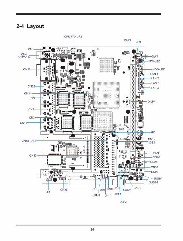
2-4 Layout
CN
20
CN18 IDE2 CN19 IDE1
DIMM1
CPU FAN JF2
CN32
SW1
PW-LED
JKM1
CN3
CN34
CN30
CN4DC12V IN
CN29
CN28
JUSB1
CN21
JCF1
JCF2
CN9
CN11
SATA1
JUSB2
CN27
JSW1 JR1
LAN 2
HDD-LED
LAN 4
JF1CN35JI1
CN8
CN1
CN26
CN16
JB1BAT1
CN37
LAN 3
LAN 1
CN33
CN14
CN17
CN15

15
2-5 Diagram (CV763A)
CN20
CN18 IDE2
CN19 IDE1
DIMM1
CPU FAN JF2
CN32
SW1PW-LED
JKM1
CN3
CN34
CN30
CN29
CN28
CN21
JCF1
JCF2
CN9
SATA1
JUSB2
CN27
JSW1 JR1
LAN 2
HDD-LED
LAN 4
JF1CN35
CN8
CN1
CN16
JB1BAT1
CN37
LAN 3
LAN 1
CN33
CN14
CN17
CN15

16
2-5-1 Diagram (CV763B)
CN20
CN18 IDE2
CN19 IDE1
DIMM1
CPU FAN JF2
CN32
SW1PW-LED
JKM1
CN11
CN34
CN7
CN29
CN28
CN21
JCF1
JCF2
CN9
SATA1
JUSB2
CN27
JSW1 JR1
LAN 2
HDD-LED
LAN 4
JF1
CN8
CN1
CN16
JB1BAT1
CN37
LAN 3
LAN 1
CN33
CN14
CN17
CN15
JVGA2
JVGA1
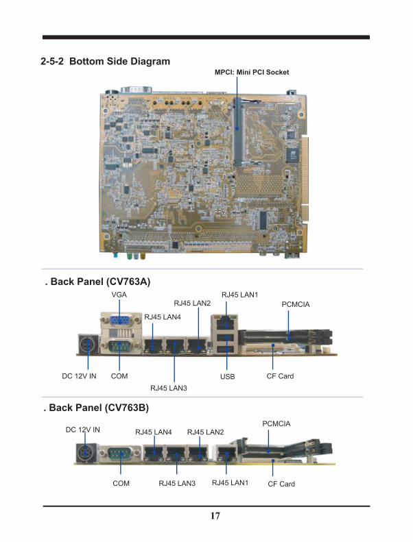
2-5-2 Bottom Side Diagram
17
MPCI: Mini PCI Socket
. Back Panel (CV763A)
DC 12V IN
VGA
COM
RJ45 LAN1
USB
PCMCIA
CF Card
RJ45 LAN4
RJ45 LAN3
RJ45 LAN2
RJ45 LAN1
RJ45 LAN2
RJ45 LAN3
RJ45 LAN4
COM
PCMCIADC 12V IN
CF Card
. Back Panel (CV763B)

18
2-6 Install Memory
This motherboard provides one 240-pin DUAL INLINE MEMORY MODULES (DIMM)socket for memory expansion available from minimum memory size of 256MB to maximum memory size of 1GB DDR2 RAM.DDR2 clock supports: DDRII200, DDRII266
Valid Memory Configurations
DS: Double Sided DIMM SS: Single Sided DIMM
Make sure the total installed memory does not exceed 1GB; otherwise, the system may hang during startup.
NOTE!
Install DDR RAM module oriented as Fig. 2.1.
Figure 2.1
DIM
M1
(BA
NK
0+B
AN
K1)
System Accept or NotDIMM1Total Memory
Min. ~ Max.
DS/SS Accept 256MB~1GB
19
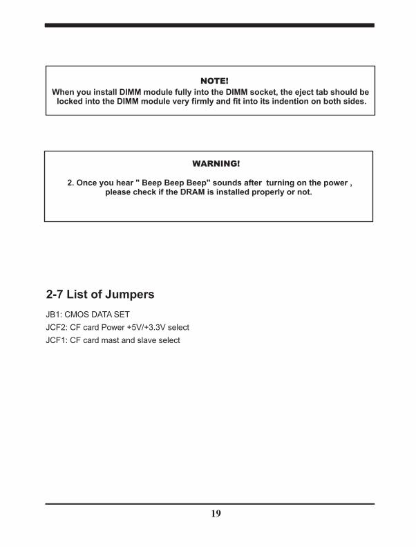
NOTE!When you install DIMM module fully into the DIMM socket, the eject tab should be locked into the DIMM module very firmly and fit into its indention on both sides.
WARNING!
2. Once you hear " Beep Beep Beep" sounds after turning on the power ,please check if the DRAM is installed properly or not.
2-7 List of JumpersJB1: CMOS DATA SETJCF2: CF card Power +5V/+3.3V selectJCF1: CF card mast and slave select

20
A jumper is ON as a closed circuit with a plastic cap covering two pins. A jumper is OFF as an open circuit without the plastic cap. Some jumpers have three pins, labeled 1, 2, and 3.You could connect either pin 1 and 2 or 2 and 3.The below figure 2.2 shows the examples of different jumper settings in this manual.
2-8 Jumper Setting Description
Figure 2.2
2-9 CMOS Data SetA battery must be used to retain the motherboard configuration in CMOS RAM. Close pin 1and pin 2 of JB1 to store the CMOS data.
To clear the CMOS, follow the procedures below:1. Turn off the system and unplug the AC power2. Remove DC 12V power cable from DC 12V power connector3. Locate JB1 and close pin 2-3 for a few seconds4. Return to its normal setting by shorting pin 1-25. Connect DC 12V power cable back to DC 12V power connector
All jumpers already have its default setting with the plastic cap inserted as ON,or without the plastic cap as OFF. The default setting may be referred in thismanual with a " " symbol .*
21
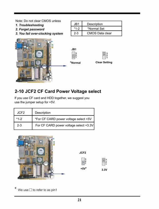
Note: Do not clear CMOS unless1. Troubleshooting2. Forget password3. You fail over-clocking system
2-10 JCF2 CF Card Power Voltage select
JCF2 Description
*1-2 *For CF CARD power voltage select +5V
2-3 For CF CARD power voltage select +3.3V
JB1 Description*1-2 *Normal Set2-3 CMOS Data clear
*Normal
JB1
1
32
JCF2
If you use CF card and HDD together, we suggest you use the jumper setup for +5V.
1
32
Clear Setting
3.3V
123
123
+5V*
* We use to refer to as pin1

22
2-11 JCF1 CF Card Master and Slave selection
JCF1 Description
*1-2 *CF Card use Master type
2-3 CF Card use Slave type
If you use CF card and HDD together, please set CF as Master and HDD as Slave.
JCF1
Master*
123
123
Slave

23
3-1 List of Connectors
This chapter provides all necessary information of the peripheral's connections,switches and indicators. Always power off the board before you install the peripherals.
Chapter-3
Connection
CN1: DC 12V-IN DIN ConnectorCN4: DC 12V-IN Connector (Share to CN1)CN30: COM1(Down side) port DB9pin ConnectorCN30: VGA (Up side) port DB15 ConnectorCN32: LAN4 RJ45 JackCN8: LAN3 RJ45 JackCN9: LAN2 RJ45 JackCN3: USB port 0/1 and LAN1 RJ45 Connector(or CN11 single RJ45)CN33: PCMCIA dual socketJKM1: PS2 Keyboard /Mouse Internal ConnectorCN19: IDE1 40 pin (2.54mm)ConnectorCN18: IDE2 44 pin (2.0mm)ConnectorCN20: CF 50 pin socketSATA1: S-ATA IDE 7pin WaferCN15: USB port 2 connectorCN17: USB port 3 connectorCN14: USB port 4 connectorCN16: USB port 5 connector (Option)CN27: USB port 7JUSB1/JUSB2:USB 6/7 port connectorCN35: DIO connector (Option)CN37: Line out /Line in/Mic-in connectorCN7: COM1 port DB9 pin connector for CV763B only (share to CN30 Down side) JVGA1, JVGA2: VGA 3pin x 2 pin header for CV763B only (share to CN30 Up side)
JF2: CPU FAN connectorJF1: System FAN connectorJI1: IR connectorCN21: DC +5/+12V output connectorCN26: I2C Bus connector (option)CN34: TV out connector (Option)MPCI1: Mini PCI socketJR1: Reset pinSW1 : System power switchJSW1 : System power switch pin headerPW LED : System power LED or pin headerJPL1: System power LED pin headerHD LED : Hard Disk LED or pin headerLAN 1/2/3/4 LED: LAN active LED
24
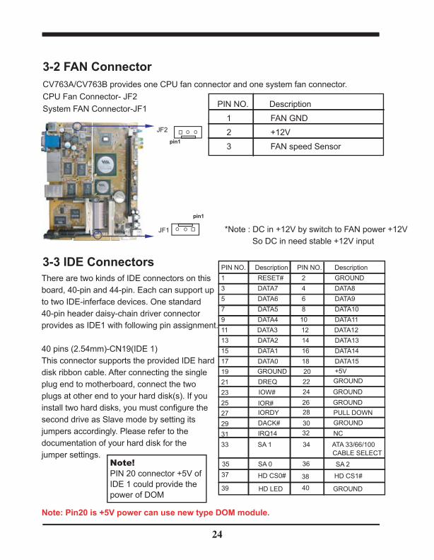
3-2 FAN ConnectorCV763A/CV763B provides one CPU fan connector and one system fan connector. CPU Fan Connector- JF2System FAN Connector-JF1
3-3 IDE ConnectorsThere are two kinds of IDE connectors on thisboard, 40-pin and 44-pin. Each can support upto two IDE-inferface devices. One standard40-pin header daisy-chain driver connectorprovides as IDE1 with following pin assignment.
40 pins (2.54mm)-CN19(IDE 1)This connector supports the provided IDE harddisk ribbon cable. After connecting the singleplug end to motherboard, connect the two plugs at other end to your hard disk(s). If youinstall two hard disks, you must configure the second drive as Slave mode by setting itsjumpers accordingly. Please refer to the documentation of your hard disk for thejumper settings.
PIN NO. Description
1 FAN GND
2 +12V
3 FAN speed Sensor
PIN NO. Description PIN NO. Description 1 RESET# 2 GROUND 3 DATA7 4 DATA85 DATA6 6 DATA97 DATA5 8 DATA109 DATA4 10 DATA1111 DATA3 12 DATA1213 DATA2 14 DATA1315 DATA1 16 DATA1417 DATA0 18 DATA151921232527293133 SA 1 34 ATA 33/66/100 CABLE SELECT
GROUND DREQ IOW# IOR# IORDY DACK# IRQ14
20222426283032
+5V GROUND GROUND GROUND PULL DOWN GROUND NC
35 36
40
37
39
38
SA 0 SA 2
HD CS0#
HD LED
HD CS1#
GROUND
pin1
JF2
pin1
JF1
Note: Pin20 is +5V power can use new type DOM module.
*Note : DC in +12V by switch to FAN power +12V So DC in need stable +12V input
Note!PIN 20 connector +5V ofIDE 1 could provide the power of DOM

353739
41
43
PIN NO. Description PIN NO. Description 1 RESET# 2 GROUND 3 DATA7 4 DATA85 DATA6 6 DATA97 DATA5 8 DATA109 DATA4 10 DATA1111 DATA3 12 DATA1213 DATA2 14 DATA1315 DATA1 16 DATA1417 DATA0 18 DATA151921232527293133 SA 1 34 ATA 33/66/100 CABLE SELECT
GROUND DREQ IOW# IOR# IORDY DACK# IRQ15
20222426283032
NC GROUND GROUND GROUND PULL DOWN GROUND NC
36
40
38SA 0 SA 2HD CS0#HD LED
HD CS1#GROUND
42
44+5VGROUND
+5VNC
25
44 pins(2.0mm)-CN18 (IDE2)
This connector supports slim type 2.5" HDD. Follow the same procedure described for theprimary IDE connector. You may also configure two hard disks as both Masters using oneribbon cable on the primary IDE connector and another ribbon cable on the secondaryIDE connector.
pin1
IDE1
CN18 (IDE2) pin1
IDE2
CN19 (IDE1)

26
3-4 Compact - Flash Memory SocketC763A/CV763B configures CompactFlash Storage Card in IDE mode.It will use IDE channel when CompactFlash card is plugged in. This socket supports CF Card Type I/II socket spec.CF Socket 50pin----CN20
18192021
22
GND(A9) GND(A8) GND(A7) +5V or +3.3V GND(A6) GND(A5) GND(A4)
35 36
3738394041
-IOW -WE(PH) INTR
-CSEL NC(-VS2) RESET
43
4544
SDA2 DREQSDA1SDA0
DACK-DASP
46
47DATA0DATA1
-PDIAGDATA8
232425
484950
DATA2 NC(-IOCS16)
GND(-CD2) GNDDATA10
DATA9
CN20
Note: Refer JCF1 /JCF2 Jumper set (CF socket share to IDE2)
PIN NO. Description PIN NO. Description 1 GND 26 GND(-CD1)2 DATA3 27 DATA113 DATA4 28 DATA124 DATA5 29 DATA135 DATA6 30 DATA146 DATA7 31 DATA157 -CS0 32 -CS18 GND(A10) 33 GND(-VS1)9 GND(-ATA_ SEL) 34 -IOR1011121314151617 GND(A3) IORDY
+5V or +3.3V
42

27
3-5 Serial Port Connector / VGA Connector
PIN NO. Description PIN NO. Description 1 DCD 6 DSR2 RXD 7 RTS3 TXD 8 CTS4 DTR 9 RI 5 GND
VGA / COM1 - CN30
CN30 :Down side RS232 Mode COM port conector D-SUB 9PIN
CN30: Up side VGA DB15 Connector Up side (D SUB 15PIN)
PIN NO. Description PIN NO. Description PIN NO. Description 1 RED 6 GND 11 NC 2 GREEN 7 GND 12 DDC DATA3 BLUE 8 GND 13 H-SYNC4 NC 9 NC 14 V-SYNC5 GND 10 GND 15 DDC CLOCK

28
3-6 External Keyboard and Mouse ConnectorThe CV763A/CV763B lets users use PS/2 mouse and PS/2 keyboard through external 5 pin header one keyboard and one mouse can be connected at one time.
. JKM1:PS2 Keyboard /mouse Internal connector
PIN NO. Description 1 KB DATA 3 NC 5 GND 7 +5 9 KB CLOCK
PIN NO. Description 2 MOUS DATA 4 KEY 6 GND 8 +5 10 MOUC CLOCK
JKM1
pin1
2

29
3-7 USB Port/ Header
CN3 (Down side) : USB 0/1port Type A Jack
PIN NO. Description
1 +5V
2 USB DATA 0/1-
3 USB DATA 0/1+
4 GND
JUSB1/JUSB2 USB 6/7 port 5pin header (2.54mm)
PIN NO. Description
1 +5V
2 USB DATA 6/7-
3 USB DATA 6/7+
4 KEY
5 GND
pin1
JUSB2
CN27
CN27: USB port 7 Type A jack
PIN NO. Description
1 +5V
2 USB DATA 7-
3 USB DATA 7+
4 GND
CN15 / CN17 / CN14 / CN16: USB port 4 pin(1.25mm Wafer connector)
PIN NO. Description
1 +5V
2 USB DATA 2/3/4/5-
3 USB DATA 2/3/4/5+
4 GND
pin1
CN15
CN17
CN3
CN16pin1
CN14

30
3-8 LAN PortThe Fast Ethernet controller provides 32-bit performance, PCI bus master capability, and full compliance with IEEE 802.3 10/100Based-T specification.For 10/100Base-T operation, please connect the network connection by plugging one end ofthe cable into the RJ-45 jack of the CN3 Connector.Besides 10/100 Base-T, CV763A/CV763B can provide Giga LAN solution through CN3once equipped with Intel 82541GI/PI/ER chipset.
. CN32/CN/8/CN9/CN3(Up side) (or single RJ45) :LAN Giga/100Mb Jack
PIN NO. Description PIN NO. Description 1 TD0-/TX+ 5 TD2-/NC 2 TD0+/TX- 6 TD2+/RX- 3 TD1-/RX+ 7 TD3-/NC 4 TD1+/NC 8 TD3+/NC
LAN LedRJ45 LAN1 Connector--- LED define Giga/100/10MB Conector
Back side connectorIndicate
Red LED Orange LED Green LEDGIGA LAN Link(light)
100Mb LAN Link(light)
10Mb LAN Link(light)
Fron side LAN1 LED Header
Indicate LAN10/100/1000BT Actived (light)
RJ45 LAN1 Connector--- LED define 10/100MB Conector
Back side connector
Indicate
GREEN LED GREEN LED
100Mb LAN Link(light)
10Mb LAN Link(light)
Fron side LAN1 LED Header
Indicate LAN10/100BT Actived (light)
RJ45 CN3
ORANGE LEDORANGE LEDLink

31
3-9 Audio Port ConnectorThe CV763A/CV763B has an on-board AC'97 3D sound interface. There are the connectors of LINE OUT, MIC-IN and LINE-IN connectors.The MIC-IN Jack and LINE-IN header are for audio sound input. The LINE-OUT connector is a 4-pin Jack for audio sound output.
PIN NO. Description
1 GND
2 FRONT OUT-L
3 NC
4 NC
5 FRONT OUT-R
. CN29(Phone Jack) -----Line-OUT(3.5mm Phone jack or 5pin 2.54mm header)
PIN NO. Description
1 GND
2 MIC-PW
3 GND
4 NC
5 MIC-IN
. CN28 (Phone Jack) -----MIC-IN (3.5mm Phone jack or 5pin 2.54mm header)
MIC-IN CN28
Speak out CN29
PIN NO. Description
1 Line-out-R
3 GND
5 Line-in-R
7 Mic-in
. CN37: Line-out / Line-in / MIC-in Header (2x4pin 2.0mm Header)
PIN NO. Description
2 Line-out-L
4 GND
6 Line-in-L
8 Mic-in
Note: If phone jack plunge into CN29 of the
signal will disabled CN37 pin 1/2 pin1
CN37

Note : Please refer to page 33 for DIO/WDT sample code .The system will be issue reset .when WDT is enable the hardware start down counter to zero
PIN NO. Description PIN NO. Description 1 DI-0 2 DO-3 3 DI-1 4 DO-2 5 DI-2 6 DO-1 7 DI-3 8 DO-0 9 GND 10 +5V
. CN35: WDT/DIO Function port (2 x 5 2.0mm Header)(option)(TBD) CN35 Digital Input / Output Connector
32
3-10 WDT/DIO Function port
pin1
CN35pin10
Logic 0 Level :+0.5V Max , Logic 1 Level : +4V Min

33
3-11 WDT/DIO Sample Code:
Compile platform:TC30 & DOS 6.22 // Sample.cpp : Defines the entry point for the console application. // #include "stdafx.h" #include "conio.h" #include <string.h> #include <stdlib.h> #include <iostream> #include "W75IO.h" /* include W75IO.h */ #define DEMO_DI 1 #define DEMO_DO 2 #define DEMO_WDT 3 #define DEMO_EXIT 4 /* demo function */ int menu(); BOOL W75IO_init(); void W75IO_DO(); void W75IO_DI(); void W75IO_WDT(); int stoi(char* str) { if (( strlen(str) < 0 ) || ( strlen(str) >= 3 )) return -1; int value = 0; for (int i=0; i<strlen(str) ;i=i+1) { int result=0; switch (str[i]) { case '0':result=0; break; case '1':result=1;break; case '2':result=2;break; case '3':result=3;break; case '4':result=4;break; case '5':result=5;break; case '6':result=5;break; case '7':result=7;break; case '8':result=8;break; case '9':result=9;break; case 'a': case 'A':result=10;break; case 'b': case 'B':result=11;break; case 'c': case 'C':result=12;break; case 'd': case 'D':result=13;break; case 'e': case 'E':result=14;break; case 'f': case 'F':result=15;break;

34
default: result=-1; break; } if (result == -1) return -1; if (strlen(str) == 1 ) value=value+result; if (strlen(str) == 2 ) { if ( i == 0 ) { value=value+result*16; } if ( i == 1 ) { value=value+result; } } } return value; } BOOL W75IO_init() { /* First step :to init W75IO.DLL */ if (InitializeW75IO()) { /* init onboard W75IO chipset */ if (InitInternalW75IO()) return TRUE; else { printf("ERROR:init Onboard W75IO chipset!!!!.\n"); return FALSE; } } else { printf("ERROR:Can't init W75IO.DLL!!!.\n"); return FALSE; } return FALSE; } void W75IO_DO() { int value; printf("Please enter your want output value (0-255) \n"); cin>>value; /* use onboard W75IO output value*/ InterDigitalOutput(value); } void W75IO_DI() { /* read & show onboard W75IO input value*/

35
printf("read input input value %d\n",InterDigitalInput()); getch(); } void W75IO_WDT() { /* get WDT timer value*/ int value; printf("Please enter WatchDog Timer value (0-255)\n"); cin>>value; /* check value */ int timer=value; if (timer > 255) { printf("must be > 255\n"); getch(); return; } /* sete onboard W75IO use secord as WatchDog Timer unit */ SetInterWDTUnit(FALSE); /* Enable onboard W75IO WatchDog Timer */ EnableInterWDT(timer); /* show message... */ for (int i=0;i<timer;i++) { printf("the System will reboot after %3d sec ....\n",timer-i); Sleep(1000); } } int menu() { int iOption; /* First clean screen */ system("cls"); /* show demo menu()*/ printf("\n"); printf("---------------------------------- \n"); printf("Sample W75IO Demo Program \n"); printf("-----------------------------------\n"); printf("1.DI\n"); printf("2.DO\n"); printf("3.WatchDog\n"); printf("4.Exit\n"); printf("----------------------------------- \n"); printf("Please select demo function(1-4)?"); /* get user select */ cin>>iOption; return iOption;

36
} int main(int argc, char* argv[]) { /* get user enter value*/ if (W75IO_init()) { while (1) { int option =menu(); if ( option == 4 ) break; switch (option) { case DEMO_DI: W75IO_DI(); break; case DEMO_DO: W75IO_DO(); break; case DEMO_WDT: W75IO_WDT(); break; case DEMO_EXIT: break; } } } return 0; }

37
3-12 IR Connector This built-in IR connector supports the optional wireless transmitting and receiving infraredmodule. It supports Infra-red Data Association (IrDA) and Amplitude Shift Keyed IR (ASKIR).You can configure the setting through the BIOS setup to use the IR function. (see Chapter 4)
. JI1: IR connector ---5pin (1.25mm Wafer connector) IR : ASKIR / IRDA
PIN NO. Description 1 +5VSB 2 FIR 3 IRRX 4 GND 5 IRTX
3-13 Serial ATA. SATA1: S-ATA IDE 7pin Wafer
pin1JI1 IR
PIN NO. Description
1 GND
2 DATA TX+
SATA1
3 DATA TX-
4 GND
5 DATA RX-
6 DATA RX+
7 GND

38
PIN NO. Description
1 +3.3V
2 GND
3 I2C CLK
4 I2C DATA
. CN26: I C Bus connector 4pin (1.25mm Wafer connector)2
3-14 I C Bus Connector2
pin1
CN26
PIN NO. Description
1 LUMA-out
2 CHROMA-out
3 CVBS
4 GND
. CN34 : TV-OUT S-VIDEO (4pin 1.25mm Wafer)(option)
3-15 TV-OUT S-VIDEO Connector
pin1
CN34

39
3-16 DC 12V IN and DC out
PIN NO. Description
1,2 +12V DC-IN
3,4 GND
. CN1: DC 12V-IN External Connector (4pin mini din connector)
CN1DC 12V IN
PIN NO. Description
3,4 +12V DC-IN
1,2 GND
. CN4: DC 12V-IN Internal Connector (4pin connector) ( For option connector)
3-17 DC +5/+12V output connector
PIN NO. Description
1 +5V
2 GND
3 GND
4 +12V*
. CN21 : DC +5/+12V output connector (2.5mm Wafer)
CN21
* Note: DC in +12V by switch to DC-out voltage +12V
So DC in need stable +12V input
40
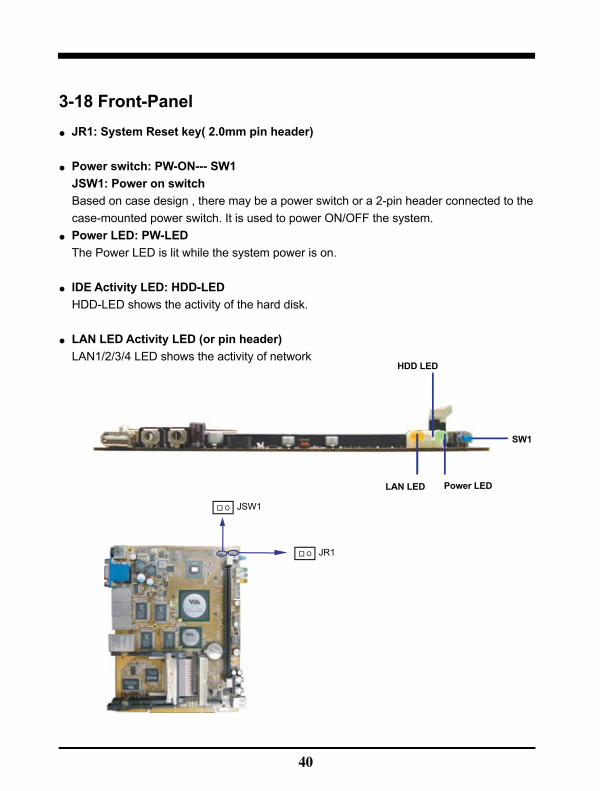
3-18 Front-Panel . JR1: System Reset key( 2.0mm pin header)
. Power switch: PW-ON--- SW1 JSW1: Power on switch Based on case design , there may be a power switch or a 2-pin header connected to the case-mounted power switch. It is used to power ON/OFF the system. . Power LED: PW-LED The Power LED is lit while the system power is on.
. IDE Activity LED: HDD-LED HDD-LED shows the activity of the hard disk.
. LAN LED Activity LED (or pin header) LAN1/2/3/4 LED shows the activity of network
SW1
HDD LED
LAN LED Power LED
JR1
JSW1

41
The BIOS is a program located in the Flash Memory on the motherboard. This program is a bridge between motherboard and operating system. When you start the computer, the BIOS program gains control. The BIOS first operates an auto-diagnostic test called POST (Power on Self Test) for all the necessary hardware, it detects the entire hardware devices and configures the parameters of the hardware synchronization. After these tasks are completed, BIOS will give control of the computer back to operating system (OS). Since the BIOS is the only channel for hardware and software to communicate with, it is the key factor of system stability and of ensuring your system performance at best.
Chapter 4Introduction of BIOS
In the BIOS Setup main menu of Figure 4-1, you can see several options. We will explain these options in the following pages. First, let us see the function keys you may use here:. Press <Esc> to quit the BIOS Setup.. Press (up, down, left, right) to choose the option you want to confirm or modify.. Press <F10> to save these parameters and to exit the BIOS Setup menu after you complet the setup of BIOS parameters.. Press Page Up/Page Down or +/- keys to modify the BIOS parameters for the active option.
4-1 Enter Setup Power on the computer and press <Del> immediately to enter Setup.
If the message disappears before your respond but you still wish to enter Setup, restart the system by turning it OFF then ON button on the system case. You may also restart the system by simultaneously pressing <Ctrl>, <Alt> and <Delete> keys. If you do not press the keys at the proper time and the system does not boot, an error message will display and you will be asked to
Press <F1> to continue, <Ctrl-Alt-Esc> or <Del> to enter Setup

42
4-2 Getting HelpMain MenuThe on-line description of the highlighted setup function is displayed at the bottom of the screen.
Status Page Setup Menu/ Option Page Setup MenuPress F1 to pop up a small help window that describes the appropriate keys to use and the possible selections for the highlighted item. To exit the Help Window, press <Esc>.
4-3 The Main Menu Once you enter Award BIOS CMOS Setup Utility, the Main Menu will appear on the screen. The Main Menu has fourteen setup functions and two exit choices. Use arrow keys to select among these items. Press <Enter> to accept or enter the sub-menu.
Phoenix-AwardBIOS CMOS Setup Utility
Standard CMOS Features
Advanced BIOS Features
Advanced Chipset Features
Integrated Peripherals
Power Management Setup
PnP/PCI Configurations
PC Health Status
Frequency/Voltage Control
Load Fail-Safe Defaults
Load Optimized Defaults
Set Supervisor Password
Set User Password
Save & Exit Setup
Exit Without Saving
Esc : Quit ↑↓→ ← : Select ItemF10 : Save & Exit Setup
Time, Date, Hard Disk Type…
F9 : Menu in BIOS

43
Standard CMOS FeaturesThis Menu is for basic system configurations.
Advanced BIOS FeaturesThis menu is to set the Advanced Features available in your system.
Advanced Chipset FeaturesThis menu is to change the values in the chipset registers and optimize your system performance.
Integrated PeripheralsThis menu is to specify your settings for integrated peripherals.
Power Management SetupThis menu is to specify your settings for power management.
PnP/PCI configurationsThis entry appears if your system supports PnP/PCI.
PC Health StatusThis entry shows your PC health status.
Frequency/Voltage ControlThis menu is to specify your settings for Miscellaneous Control.
Load Optimized DefaultsUse this menu to load the BIOS default values that are factory settings for optimal system operation performance. It is provided for the skillful users who want to push the motherboard to get better performance. The Optimized setting does not go through all the reliability and compatibility tests, it is verified only with limited configurations and loading (for example, a system that is equipped with only one VGA card and one DIMM. Do not use Optimized setting unless you fully understand the items in chipset setup menu.

[EGA/VGA]
44
Load Standard DefaultsUse this menu to load the BIOS default values for the optimum system performance.Standard Defaults settings are relatively more reliable than Optimized Defaults.All the product verifications, compatibility test reports and manufacture quality controls are based on "Standard Defaults". We suggest you to use this settingfor normal operation. "Standard Defaults" is not the slowest setting for this motherboard. If you need to verify an unstable problem, you may manually set the parameter in "Advanced Chipset Features" to get slower and safer setting.
Set Supervisor/User PasswordThis menu is to set User and Supervisor Passwords.
Save & Exit SetupSave CMOS values modified to CMOS and exit setup.
Exit Without SavingAbandon all the CMOS values modified and exit setup.
4-4 Standard CMOS FeaturesThe items in Standard CMOS Setup Menu are divided into several categories. Each category includes no, one or more than one setup items. Use the arrowkeys to highlight the item and then use the <PgUp> or <PgDn> keys to select the value you want to modify with this item.
Phoenix - AwardBIOS CMOS Setup UtilityStandard CMOS Features
Item Help May 5 2006
10 : 59 : 36
IDE Channel 0 Master
[No Errors]
Base Memory
Extended Memory Total Memory
Menu Level >
Change the day, moth,
year and century
↑↓→←:Move Enter:Select +/-/PU/PD:Value F10:Save ESC:Exit F1:General Help
F5:Previous Values F6:Fail-Safe Defaults F7:Optimized Defaults
Time (hh:mm:ss)
Date (mm:dd:yy)
[ None ]
VideoHalt On
1024K
640K
IDE Channel 0 Slave [ None ] IDE Channel 1 Master [ None ] IDE Channel 1 Slave [ None ] IDE Channel 2 Master [ None ] IDE Channel 3 Master [ None ]
65472K

45
4-5 Advanced BIOS Features
Virus WarningThe VIRUS Warning feature can help you protect IDE Hard Disk boot sector. If this function is enabled, BIOS will show a warning message on screen and alarm beep when somenoe attemps to write data into this area without permission. Disabled (default) No warning message appears when anything attempts to access the boot sector or hard disk partition table. Enabled Activate automatically when the system boots up. The system will show the warning message if anything attempts to access the boot sector of hard disk partition table.
Phoenix-AwardBIOS CMOS Setup UtilityAdvanced BIOS Features
Item HelpVirus Warning [Disabled]CPU L1 & L2 Cache CPU L2 Cache ECC Checking
Quick Power On Self Test [Enabled]First Boot Device Second Boot Device [Hard Disk] Third Boot Device [CDROM]Boot Other Device [Enabled]Boot Up NumLock Status [On]Typematic Rate Setting Typematic Rate (Chars/Sec) [6]Typematic Delay (Msec) [250]Security Option [Setup]
OS Select For DRAM > 64MB [Non - OS2]
Video BIOS Shadow [Enabled]
Small Logo (EPA) Show
Menu Level >
Allows you to choosethe VIRUS warning
feature for IDE Hard Disk boot sector protection. If thisfunction is enabledand someone attempt to write data into thisarea, BIOS will show awarning message onscreen and alarm beep
↑↓→← :Move Enter:Select +/- /PU/PD:Value F10:Save ESC:Exit F1:General Help
F5:Previous Values F6:Fail-Safe Defaults F7:Optimized Defaults
Full Screen LOGO Show [Enabled]
XX
Hard Disk Boot Priority
[Enabled]
[Disabled]
[USB-FDD]
[Disabled]
[Press Enter]
[Enabled]

46
4-6 Advanced Chipset FeaturesThe Advanced Chipset Features Setup option is used to change the values of the chipset registers. These registers control most of the system options in the computer.
Item HelpDRAM Clock/Drive Control [Press Enter]AGP & P2P Bridge Control [Press Enter]
Memory Hole [Disabled]System BIOS Cacheable [Enabled]Video RAM Cacheable [Disabled] Menu Level >>
↑↓→←:Move Enter:Select +/-/PU/PD:Value F10:Save ESC:Exit F1:General HelpF5:Previous Values F6:Fail-Safe Defaults F7:Optimized Defaults
The menu is to include settings for the chipset dependents features.These features are related to system performance. Make sure you fully understand the items contained in this menu before you change anything. You may change the parameter settings toimprove system performance. However, it may make your system unstable if the setting is not correct for your system configuration.
Phoenix- AwardBIOS CMOS Setup UtilityAdvanced Chipset Features
4-6-1 DRAM Clock/Drive Control
Item HelpCurrent FSB Frequency
100 MHz
Current DRAM Frequency 200 MHz
DRAM Clock
Menu Level >>
↑↓→←:Move Enter:Select +/-/PU/PD:Value F10:Save ESC:Exit F1:General Help
Phoenix- AwardBIOS CMOS Setup UtilityDRAM Clock/Drive Control
F5:Previous Values F6:Fail-Safe Defaults F7:Optimized Defaults
[200 MHz]

Direct Frame Buffer
47
4-6-2 AGP & P2P Bridge Control
Item HelpVGA Share Memory Size [64M][Enabled]
Menu Level >>
↑↓→←:Move Enter:Select +/-/PU/PD:Value F10:Save ESC:Exit F1:General HelpF5:Previous Values F6:Fail-Safe Defaults F7:Optimized Defaults
Phoenix- AwardBIOS CMOS Setup UtilityAGP & P2P Bridge Control
4-7 Integrated Peripherals
Item Help VIA OnChip IDE Device [Press Enter]VIA OnChip PCI Device [Press Enter]Super IO Device [Press Enter]
Menu Level >>
↑↓→←:Move Enter:Select +/-/PU/PD:Value F10:Save ESC:Exit F1:General Help
Phoenix- AwardBIOS CMOS Setup UtilityIntegrated Peripherals
F5:Previous Values F6:Fail-Safe Defaults F7:Optimized Defaults

48
4-7-1 VIA OnChip IDE Device Phoenix-AwardBIOS CMOS Setup Utility
VIA OnChip IDE Device
Item HelpOnChip SATA [Enabled]SATA Mode IDEIDE DMA transfer access [Enabled]OnChip IDE Channe10 [Enabled]OnChip IDE Channe11 [Enabled]IDE Prefetch Mode [Enabled]Primary Master PIO [Auto] Primary Slave PIO [Auto] Secondary Master PIO [Auto]Secondary Slave PIO [Auto]Primary Master UDMA [Auto] Primary Slave UDMA [Auto] Secondary Master UDMA [Auto]Secondary Slave UDMA [Auto]IDE HDD Block Mode [Enabled]
Menu Level >>
↑↓→←:Move Enter:Select +/-/PU/PD:Value F10:Save ESC:Exit F1:General Help
F5:Previous Values F6: Fail-Safe Defaults F7:Optimized Defaults
4-7-2 VIA OnChip PCI Device
VIA-3058 AC97 AUDIOThis item allows you to decide to enable/disable to support AC97 Audio.
Phoenix - AwardBIOS CMOS Setup Utility
-
Item Help VIA-3058 AC97 AudioOnChip USB Controller [All Enabled]OnChip EHCI Controller [Enabled]USB Emulation [ON]USB Keyboard Support EnabledUSB Mouse Support Enabled
[Auto]
Menu Level >>
↑↓→←:Move Enter:Select +/-/PU/PD:Value F10:Save ESC:Exit F1:General Help
F5:Previous Values F6: Fail-Safe Defaults F7:Optimized Defaults
xx
If your IDE hard drive supports block mode select Enable forautomtic detection ofthe optimal numberof block read/writes persector the drivecan support
VIA OnChip IDE Device

49
4-7-3 Super IO Device
[3F8/IRQ4]
Phoenix-AwardBIOS CMOS Setup UtilitySuper IO Device
Item HelpOnboard Serial Port 1
Menu Level >>
↑↓→←:Move Enter:Select +/-/PU/PD:Value F10:Save ESC:Exit F1:General HelpF5:Previous Values F6: Fail-Safe Defaults F7:Optimized Defaults
4-8 Power Management SetupThe Power Management Setup allows you to configure your system to most effectively energy saving while operating in a manner consistent with yourown style of computer use.
IRQ / Event Activity DetectPlease refer to section4-8-1

50
4-8-1 IRQ / Event Activity Detect
4-8-1.1 IRQs Activity Monitoring
IRQs Activity MonitoringPlease refer to section4-8-1.1

4-9 PnP / PCI Configuration Setup
51
This section describes how to configure the PCI bus system. PCI, or Personal ComputerInterconnect, is a system which allows I/O devices to operate at the speed the CPU itselfkeeps when CPU communicates with its own special components. This section covers some very technical items and we strongly recommended that only experienced usersshould make any change to the default settings.
Resource Controlled ByThe Award Plug and Play BIOS can automatically configure all of the boot and Plug and Play compatible devices. However, this capability means absolutely nothing unless you are using a Plug and Play operating system such as Windows 95/98. If you set this field to "manual", choose a specific resource by going into each sub menu that follows this field (a sub menu is preceded by a ">").The settings are Auto (ESCD) or Manual.
IRQ ResourcesWhen resources are controlled manually, each system interrupt is assigned a type, depending on the type of device using the interrupt.
PCI/VGA Palette SnoopLeave this field at Disabled. The settings are Enabled or Disabled.

52
4-10 PC Health StatusThis section shows the status of your CPU, Fan, and overall system. This is only available when there is Hardware Monitor function onboard.
Show PC Health in PostDuring Enabled, it displays information list below. The choice is either Enabled or DisabledCurrent CPU Temperature/Current System Temp/Current FAN1,FAN2 Speed/ Vcore/3.3V/+5V/+12VThis will show the CPU/FAN/System voltage chart and FAN Speed
53
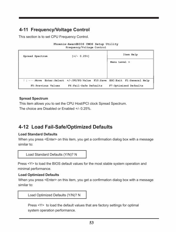
4-11 Frequency/Voltage ControlThis section is to set CPU Frequency Control.
Spread SpectrumThis item allows you to set the CPU Host/PCI clock Spread Spectrum.The choice are Disabled or Enabled +/- 0.25%.
Phoenix-AwardBIOS CMOS Setup UtilityFrequency/Voltage Control
Item Help
Menu Level >
↑↓→←:Move Enter:Select +/-/PU/PD:Value F10:Save ESC:Exit F1:General HelpF5:Previous Values F6:Fail-Safe Defaults F7:Optimized Defaults
4-12 Load Fail-Safe/Optimized DefaultsLoad Standard DefaultsWhen you press <Enter> on this item, you get a confirmation dialog box with a message similar to: Load Standard Defaults (Y/N)? N
Load Optimized DefaultsWhen you press <Enter> on this item, you get a confirmation dialog box with a messagesimilar to:
Load Optimized Defaults (Y/N)? N
Press <Y> to load the default values that are factory settings for optimal system operation performance.
Spread Spectrum [+/- 0.25%]
Press <Y> to load the BIOS default values for the most stable system operation andminimal performance.

54
4-13 Set Supervisor/ User PasswordYou can set supervisor password, user password, or both. The differences are:
Supervisor password: You can enter the setup menus and change the options.User password: You can enter the setup menus but do not have the right to change the options. When you select this function, the following message will appear at the center of the screen to assist you in creating a password. ENTER PASSWORD:Type the password, up to eight characters in length, and press <Enter>. The passwordtyped will clear any previous password from CMOS memory. You will beasked to confirm the password. Type the password again and press <Enter>. You mayalso press <Esc> to abort the selection without entering password. To disable a password, just press <Enter> when you are prompted to enter thepassword. A message will confirm if you want to disable the password. Once thepassword is disabled, the system will boot and you can enter Setup menus freely. PASSWORD DISABLED.When a password has been enabled, you have to enter it every time before youenter the Setup. This prevents an unauthorized person from changing any part ofyour system configuration.
Additionally, when a password is enabled, you can also have the BIOS to request a password at every time when your system is rebooted. This would prevent the unauthorized user.
You can determine if the password is required within the BIOS Features Setup Menuand its Security option. If the Security option is set to "System", the password will be required both at boot and at entry to Setup. If set to "Setup", the password is required only at the entry to Setup.

55
Chapter 5
DRIVER INSTALLATIONThere is a SYSTEM INSTALL CD disk in the package. This CD has all the drivers you needand some free application programs and utility programs. In addition, this CD also includes an auto-detect software which can tell you which hardware is installed and which driver is needed so that your system can function properly. We call this auto detect software SYSTEM INSTALL.
SYSTEM INSTALL Supports WINDOWS
98/98SE/ME/2000/XPInsert the CD into your CD-ROM drive and the SYSTEM INSTALL Menu should appear as below. If the menu does not appear, double-click MY COMPUTER and double-click CD-ROM drive or click START, click RUN, and type X:\AUTORUN.EXE (assuming X is your CD-ROM drive).
From MAGIC INSTALL MENU you may make 3 selections:1 . Auto detect main board and OS Into auto install driver Menu2 . Explore CD to explore the contents of the CD3 . EXIT to exit from SYSTEM INSTALL menu

56
Auto install driver Menu
1. VIA 4 IN 1 install VIA IDE/AGP/IRQ ROUTING/INF driver2. VGA install on-board VGA driver3. SOUND install AC97 Audio Codec Installing driver 4. USB2.0 install VIA USB2.0 hardware Installing driver5. LAN to LAN install driver readme file6. DIRECTX9 To install DirectX9 driver readme file7.OTHERS To PenMount 6000 install driver readme file
Note: PenMount 6000 DRIVER IS TO BE INSTALLED UNDER WIN 2000/XP ONLY.Each selection is illustrated as below:

57
1.Click VIA 4 IN 1 when System Install MENU appears.
2.Click NEXT when VIA Service Pack Wizard appears.
3.License Agreement. Click NEXT. 4. Choose all the drivers. Click NEXT.
Note: VIA AGP Driver IS TO BE INSTALLED UNDER WIN98 ONLY.
5-1 VIA 4 IN 1 Install VIA IDE/AGP/ INF Driver
IDE : VIA ATAPI VENDOR SUPPORT DRIVER IS USED TO FIX COMPATIBILITY ISSUE FOR IDE DEVICES.AGP: VIA AGP DRIVER IS TO BE INSTALLED. IF YOU ARE USING AN AGP VGA CARD, VIAGART.VXD WILL PROVIDE SERVICE ROUTINES TO YOUR VGA DRIVER AND INTERFACE DIRECTLY TO HARDWARE, PROVIDING FAST GRAPHIC ACCESS.INF : VIA REGISTRY DRIVER IS TO BE INSTALLED UNDER WINDOWS. THE DRIVER WILL ENABLE VIA POWER MANAGERMENT CONTROLLER.

58
5.Installing Components List. Click NEXT. 6. This is to announce the Copy Right. Click NEXT.
7.Click Finish to restart computer.
NOTE: SYSTEM INSTALL will auto detect file path X:\driver\VIA\CN700\4IN1\setup.exeThis driver supports WINDOWS 95\98\98SE\NT4.0\2000\XP

59
1. Click VGA when System Install MENU appears.
2. Click NEXT when VIA/S3 CN700 Driver Setup appears.
5-2 VGA INSTALL CN700 VGA Driver
3. This VIA/S3 CN700 Driver install willbegin copying the driver files. Click NEXT.
Note: When you install driver ,the “Hardware Installation”dialog in Windows XP will appear , click “countine Auyway”.
4. Click FINISH to Restart Computer.
NOTE: The path of the file For WINDOWS 98/98SE/MEX:\driver\VIA\CN700\VGA\WIN98me\SETUP.EXEFor WINDOWS 2000/XP X:\driver\VIA\CN700\VGA\WIN2KXP\SETUP.EXE

60
1.Click SOUND when System Install MENU appears.
2. Click NEXT install VIA AC97 Audio Driver
5-3 SOUND Install VIA Audio Codec Driver for VIA
3. Click NEXT install VIA AC97 Audio Driver
4. Click FINISH to Restart Computer.
NOTE: The path of the file For WIN98/ME/2K\XP X:\ driver\via\viaudio\setup.exe

61
1.Click USB2.0 when System Install MENU appears.
2. Click NEXT install USB2.0 Driver
5-4 USB2.0 install VIA USB2.0 Installing driver
3. Click NEXT install VIA USB2.0 Driver 4. Click FINISH to Restart Computer.
NOTE: The path of the file For WIN98/ME/2K\XPx:\ driver\via\CN700\USB20\setup.exe
NOTE: When you install driver for USB2.0under Windows 2000.Please install SP4 first.When you install driver for USB2.0 under Windows XP.Please install SP1 first.

62
5-5 HOW TO DISABLE ON-BOARD SOUNDEnter BIOS SETUP. Choose INTEGRATE PERIPHERALS. Choose On-Chip DeviceFUNCTION. Choose " AC97 Audio Disable " on-board sound function by pressingPAGE DOWN KEY to Disable.
In DOS ModeSTEP 1. Prepare a boot disc. (you may make one by clicking START, clicking RUN, typing SYS A: , and clicking OK)STEP 2. Copy utility program to your boot disc. You may copy it from DRIVER CD X:\Diver\bios\AWDFLASH.EXE or download it from our web site.STEP 3. Copy the latest BIOS for CV763A from our web site to your boot disc.STEP 4. Insert your boot disc into A: Start the computer and type "Awdflash A:\CV763Axxx.BIN/SN/PY/CC/R" CV763Axxx.BIN is the file name of the latest BIOS. It may be CV763AA1. BIN or CV763AA2.BIN SN means don't save the current BIOS data PY means renew the current BIOS data CC means clear the current CMOS data R means restart computerSTEP 5. Press ENTER and the BIOS will be updated, computer will restart automatically.
5-6 HOW TO UPDATE BIOS
63
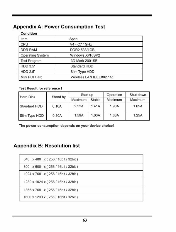
Appendix A: Power Consumption TestConditionItem SpecCPU V4 - C7 1GHzDDR RAM DDR2 533/1GB Operating System Windows XPP/SP2Test Program 3D Mark 2001SEHDD 3.5" Standard HDDHDD 2.5" Slim Type HDDMini PCI Card Wireless LAN IEEE802.11g
Hard Disk Stand by
Standard HDD 0.10A
Slim Type HDD 0.10A
Test Result for reference !
Start up OperationStable
Shut downMaximum Maximum Maximum
2.52A 1.41A
1.59A 1.03A
1.98A 1.65A
1.63A 1.25A
The power consumption depends on your device choice!
Appendix B: Resolution list
640 x 480 x ( 256 / 16bit / 32bit )
800 x 600 x ( 256 / 16bit / 32bit )
1024 x 768 x ( 256 / 16bit / 32bit )
1280 x 1024 x ( 256 / 16bit / 32bit )
1366 x 768 x ( 256 / 16bit / 32bit )
1600 x 1200 x ( 256 / 16bit / 32bit )


![EPOS solutions.1].pdf · EPOS solutions. PC TOUCH SCREEN BOARD CPU Via C7 1.5GHz. Chipset Via CN700 (NB) + Via VT8237R (SB) HDD 2.5” SATA 80G MEMORY DDR2 512MB (Max. 1GB) Size 15”](https://static.fdocuments.us/doc/165x107/5f0d43977e708231d4397b89/epos-1pdf-epos-solutions-pc-touch-screen-board-cpu-via-c7-15ghz-chipset.jpg)