CUTTING EDGE TECHNOLOGY DELIVERING UNIQUE …
28
Carl Zeiss SMT – Nano Technology Systems Division ZEISS CrossBeam ® SERIES The ultimate 3D research tool that combines FIB and GEMINI ® technology to one extraordinary powerful system with unlimited analytical capabilities Enabling the Nano-Age World ® CUTTING EDGE TECHNOLOGY DELIVERING UNIQUE SOLUTIONS
Transcript of CUTTING EDGE TECHNOLOGY DELIVERING UNIQUE …

C a r l Z e i s s S M T – N a n o T e c h n o l o g y S y s t e m s D i v i s i o n
ZEISS CrossBeam® SERIES
The ultimate 3D research tool thatcombines FIB and GEMINI® technology to one extraordinary powerful systemwith unlimited analytical capabilities
E n a b l i n g t h e N a n o - A g e W o r l d ®
CUTTING EDGE TECHNOLOGY DEL IVERING
UNIQUE SOLUTIONS
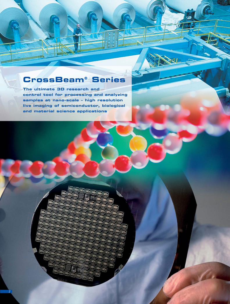
CrossBeam® SeriesThe ultimate 3D research and control tool for processing and analyzingsamples at nano-scale – high resolutionlive imaging of semiconductor, biologicaland material science applications
2

CrossBeam® Series
New dimensions with extraordinary power –
designed for ultimate 3D research and process
control
High precise – direct processing and shaping
of the specimen
Unique live imaging – during the whole range
of specimen processing, combining ultra high
resolution FESEM with high performance FIB
Ultimate cognition – unlimited analytical
capabilities at nano-scale
Perfect handling – full control of specimen
processing
Unique 3-D Views – Delivers Cutting-edge Solutions
3
1 µm
1 µm
1 µm
2 µm

CrossBeam®1540XBThe ZEISS 1540XB CrossBeam® combines the advan-
tages of the ultra high resolution, low dose GEMINI®
Field Emission Scanning Electron Microscope (FESEM)
with a high-performance, focused ion beam (FIB)
system. Applications are as diverse as subsurface root
cause failure analysis, high precision TEM sample
preparation, nano-structuring and E-beam lithography.
The system consists of live E-beam imaging during
FIB operation, a compact, five-channel gas injection
system and a large ultra-precise specimen stage, satis-
fying even the most demanding applications. It is a
state-of-the-art combination of real-time 3D analysis,
nano-scale manipulation and an imaging tool.
CrossBeam®1560XBThe large chamber system with the refined 6" super
eucentric stage and the 8" integrated airlock offers the
perfect solution for full wafers and cross sectional
semiconductor applications, and for users who need to
analyse a variety of large samples.
● Ultra high resolution FESEM with unique GEMINI®
column and high performance CANION FIB column
● CrossBeam® operation: high resolution live imaging
during milling, polishing and deposition
● Multi channel gas injection system for deposition
and enhanced or selective etching
● Super eucentric, fully motorized 6 axis stage
The Ultimate Research Tools
4
Nano-scale 3D Analysis Tool
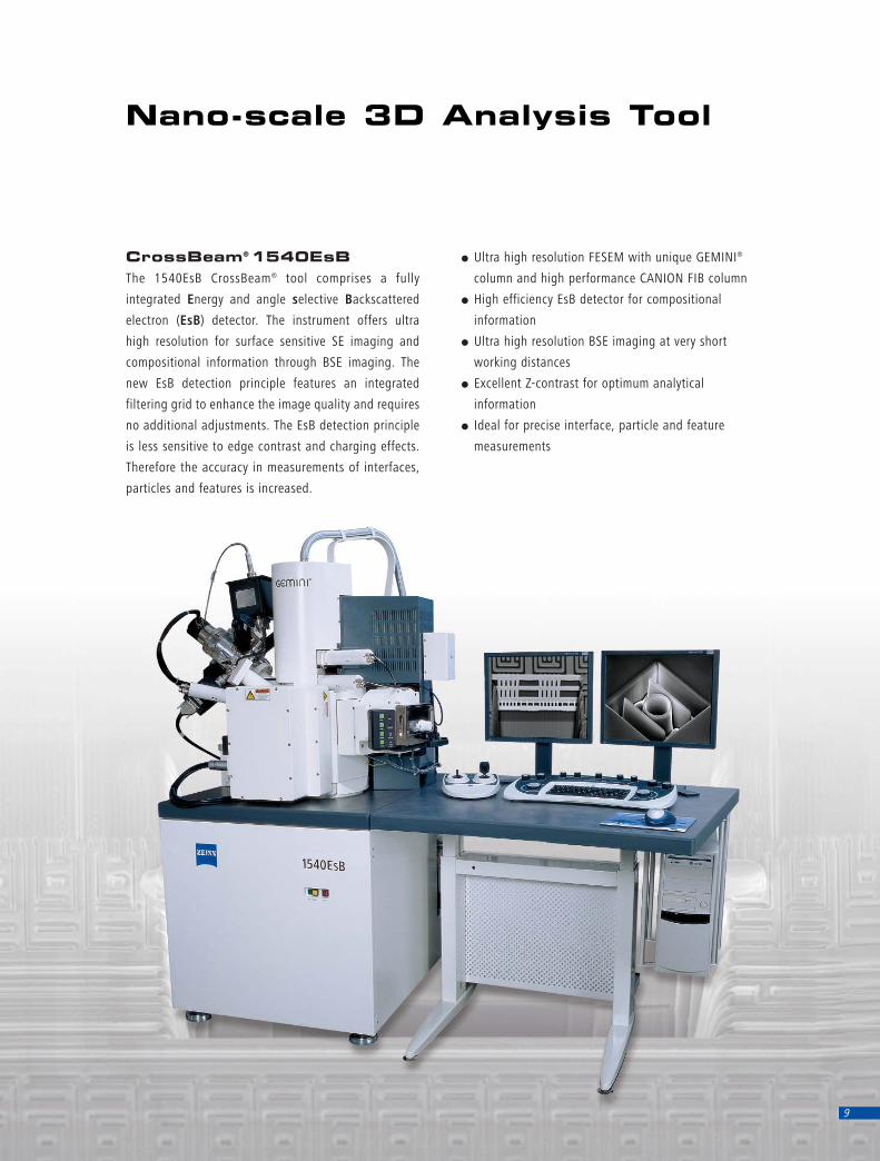
CrossBeam®1540EsBThe 1540EsB CrossBeam® tool comprises a fully
integrated Energy and angle selective Backscattered
electron (EsB) detector. The instrument offers ultra
high resolution for surface sensitive SE imaging and
compositional information through BSE imaging. The
new EsB detection principle features an integrated
filtering grid to enhance the image quality and requires
no additional adjustments. The EsB detection principle
is less sensitive to edge contrast and charging effects.
Therefore the accuracy in measurements of interfaces,
particles and features is increased.
● Ultra high resolution FESEM with unique GEMINI®
column and high performance CANION FIB column
● High efficiency EsB detector for compositional
information
● Ultra high resolution BSE imaging at very short
working distances
● Excellent Z-contrast for optimum analytical
information
● Ideal for precise interface, particle and feature
measurements
9

CANIONThe CrossBeam® series make use of the high perfor-
mance CANION FIB column. The superior ion optical
concept of the CANION FIB column provides excellent
resolution, high current densities and a large beam
voltage range between 3 kV and 30 kV. The ion beam is
generated in a high brightness LMIS (liquid metal ion
source) and focused onto the specimen by an opti-
mised electrostatic two lens system. Stabilization of the
emission current and the selection of different probe
currents is totally computer controlled. This gives the
user full advantage in automation processes and ease
of use. All alignments for different probe currents and
beam voltage settings are stored via the SmartSEMTM
operating system and can be easily selected by a click
of a button. An integrated Faraday cup allows accura-
te probe current measurements during the operation.
● Excellent imaging resolution < 7 nm
● Extended probe current range 1 pA - 50 nA
● High brightness LMIS (liquid metal ion source)
● Electrostatic two lens system
● Totally computer controlled
● Large voltage range 3 kV - 30 kV
● Integrated electrostatic high speed beam blanker
● Integrated Faraday cup for accurate probe
current measurements
● 7 mechanical apertures
Ion Optics
Ion optical layout of the CANION ion column.
5
Comparison of the physical properties of different emitter types. The CrossBeam® tool makes use of Schottky FE for the SEM column and LMIS for the FIB column.
Operating modes of the CANION ion column. Telecentric beam path for optimum imaging conditions (right) andcollimated beam path for high probe currents (left).
LMIS
Condenser lens
Apertures
Beam blanker
Faraday cup
Scan and deflection
Final lens
Emitter
Condenser lens
Aperture
Final lens
The CrossBeam® Concept
6
System LayoutThe CrossBeam® tools combine the
imaging and analytical capabilities
of a high resolution field emission
SEM (FESEM) with a high perfor-
mance FIB column into one inte-
grated instrument. In the case of
the CrossBeam® tool the final lens
of SEM is designed as a magne-
tic/electrostatic compound lens.
This layout has the advantage that
no magnetic field interferes with
the ion beam and the SEM can be
operated at nm resolution during
the ion milling process. This layout
allows full control over the total
process and gives an excellent end-
point detection and cut localization
for defect review and failure ana-
lysis.
Together with a multi-channel gas
injection system for metal and
insulator deposition and for enhan-
ced and selective etching the
CrossBeam® workstation is a very
powerful analytical and imaging
tool for a wide range of appli-
cations within the semiconductor
industry as well as for material
science and life science appli-
cations.
Schematic layout of the CrossBeam® tool. The electron beam and the ion beam coincide at a point 5 mm below the final lens of the SEM.
CrossBeam® 1540XB equipped with FIB and gas injection systemfor 5 different gases.
FIB column
CCD camera &
illumination
GEMINI® column
In-lens detector
SE detector
EDS detector
Gas injection
system (GIS)

The CrossBeam® Concept
Layout of the CrossBeam® specimen chamber. The flexible port configuration meets every analytical requirement.
BSD-port
QMS-port
GIS-port
FIB Column
EBSP/CCD-camera port
EDS-port
In-lens Detector
Universal Port
SE Detector
CCD-camera
7
Chamber DesignThe flexible chamber design of the
CrossBeam® tools provides full
compatibility to all analytical requi-
rements. Two CCD cameras monitor
the inside of the specimen chamber
to provide the operator with full
information when handling large
and special shaped samples. Many
additional ports provide the capa-
bility of adding various detectors,
airlocks and analytical equipment
making the CrossBeam® system the
ultimate 3D analysis tool.
Imaging ModesA CrossBeam® tool can operate at
three different imaging modes. By
blanking the ion beam and only
using the electron beam for imaging
the system operates as a high
resolution field emission SEM. The
second imaging mode uses the ion
beam while the electron beam is
blanked. This FIB imaging mode is
used for grain analysis, voltage con-
trast imaging and defining of mil-
ling areas. The last imaging mode is
the so called CrossBeam® operati-
on mode: Both beams are turned on
and while the ion beam is milling a
defined area, the SEM is used to
image the milling process at high
resolution in real time. This enables
the operator to control the milling
process on a nanometer scale and
to perform extremely accurate cross
sections and device modifications.
If the system is used as a
high resolution SEM only
the ion beam is blanked
and the SE signal is syn-
chronized to the SEM scan.
In this operational mode
the system can be used as a
high resolution FESEM with
no limitations.
If the system is used as a
FIB, only the SEM beam is
blanked and the signal is
synchronized to the FIB
scan. This mode is used for
channelling contrast ima-
ging, voltage contrast ima-
ging and for defining mil-
ling patterns on the sample
surface.
Both beams are scanned
completely independent of
each other and the SED
Signal is synchronized to
the SEM scan. This results
in the CrossBeam® opera-
tion feature: The ion milling
process can be imaged
using the SEM in real-time.
SEM imaging FIB imaging CrossBeam® operation

Electron Optics
Dramatic reduction of objective lens aberrations in the low kV range.
8
GEMINI®
The CrossBeam® has been built around the unique GEMINI®
lens design which has many advantages over classical lens
designs:
The most important feature is the decreasing aberrations with
decreasing beam energy. Therefore it delivers superb resolution
down to 100 V and at 30 kV its resolving power is unsurpassed.
The high-angled GEMINI® objective lens body allows 56° tilt of
large specimens (e.g. 6" wafers) at a working distance as low
as 5mm. The analytical working distance for EDS analysis with
a take-off angle of 35° is only 5 mm - suitable for high resolu-
tion imaging. The GEMINI® objective lens consists of a high
performance magnetic lens with an inserted electrostatic lens.
The GEMINI® concept has overcome the problem with classical
objective lens designs which immerses the specimen in the
magnetic field prohibiting imaging of magnetic samples. The
GEMINI® magnetic lens is shaped to minimise the magnetic
field at the specimen. Therefore high resolution imaging of
dia-, para-, or ferromagnetic samples is possible with very
short working distances.
The magnetic/electrostatic lens combination is equivalent to an
optical lens triplet which increases the incident beam aperture
angle at the specimen and hence improves resolution. The
increase of the optimum beam aperture angle also provides a
larger electron probe current and hence generates a superior
signal to noise ratio of the image. The lens control system with
integrated condenser control will always select the optimum
beam aperture for any combination of working distance and / or
selected energy. Consequently the FESEM delivers excellent
image contrast even at the resolution limit. A single-stage
beam scanning system is integrated in the GEMINI® lens, just
in front of the electrostatic lens gap. Therefore, the transverse
chromatic and other scanning aberrations have been mini-
mised. The instrument operates without distortion at TV-scan-
ning speed from the lowest (12 x) to the highest (900,000 x)
magnification. In particular, no switch-over is required bet-
ween a low magnification mode and a high resolution mode.
The GEMINI® objective lens provides outstanding
resolution and image quality, especially at low
beam voltages, without any compromise in opera-
tional convenience.
GEMINI® bias concept.
��
��
���
�������
����� �
��������� ��������������� ���
� ����������������
� ���������������
������������
��� ����� �
��� ����
������������� �
������
100 nm

Semiconductor Applications
Low voltage electron backscatter image (EsB) of a thin diffusion barrier between copper lines and oxide material in a computer chip. The electron energy is 2 kV.
Cross section through a semiconductor device. SEM image on the left and FIB image on the right. The FIB image provides additional voltage contrast information. Note the bright and dark metal lines in the right image.
10
100 nm
1 µm 1 µm
The CrossBeam® workstations deliver extraordinary
results for semiconductor applications. The CrossBeam®
workstations are designed to meet the most deman-
ding applications of failure analysis and process de-
velopment. Imaging of nonconductive samples, cross
sections and voltage contrast applications are no
problem for the CrossBeam® workstations.
The use of various detector signals and primary beams
simultaneously opens up new dimensions of informati-
on about the sample. While the electron beam genera-
tes ultimate high resolution information about the
sample surface and composition, the ion beam provi-
des data for voltage contrast and channelling contrast.

The excellent low voltage imaging capabilities of the
GEMINI® SEM column make the CrossBeam® the ideal
tool to image photo resist, polymers, oxides and other
non conductive samples in their natural state in high
resolution.
High resolution low voltage imaging of a photo resist structureon a silicon substrate. The electron energy is 0.8 kV!
Dark-field STEM image of copper plugs.
Example of a voltage contrast application to detect defects in a via chain.
SEM imaging: Cross section through a photo-resist structure. The nonconductive sample is uncoated. Accelerating voltage 1 kV. Note the depth of focus in the image.
11
100 nm
200 nm
100 nm
10 µm
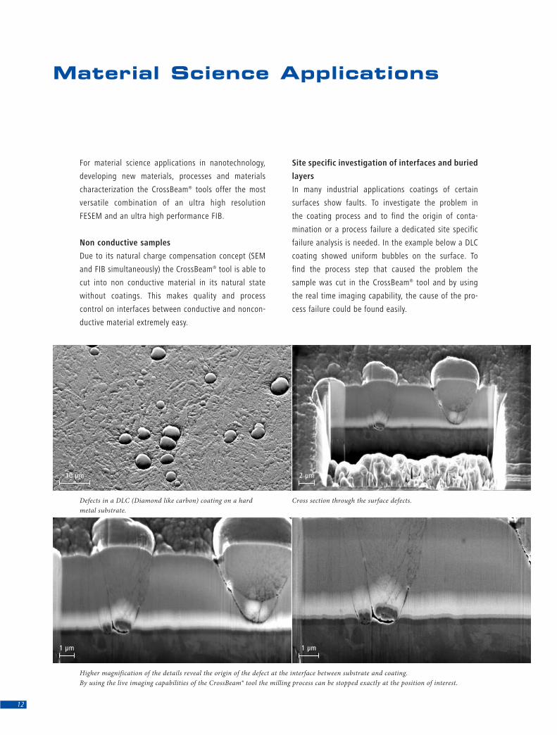
For material science applications in nanotechnology,
developing new materials, processes and materials
characterization the CrossBeam® tools offer the most
versatile combination of an ultra high resolution
FESEM and an ultra high performance FIB.
Non conductive samples
Due to its natural charge compensation concept (SEM
and FIB simultaneously) the CrossBeam® tool is able to
cut into non conductive material in its natural state
without coatings. This makes quality and process
control on interfaces between conductive and noncon-
ductive material extremely easy.
Material Science Applications
Higher magnification of the details reveal the origin of the defect at the interface between substrate and coating. By using the live imaging capabilities of the CrossBeam® tool the milling process can be stopped exactly at the position of interest.
Defects in a DLC (Diamond like carbon) coating on a hard metal substrate.
Cross section through the surface defects.
12
Site specific investigation of interfaces and buried
layers
In many industrial applications coatings of certain
surfaces show faults. To investigate the problem in
the coating process and to find the origin of conta-
mination or a process failure a dedicated site specific
failure analysis is needed. In the example below a DLC
coating showed uniform bubbles on the surface. To
find the process step that caused the problem the
sample was cut in the CrossBeam® tool and by using
the real time imaging capability, the cause of the pro-
cess failure could be found easily.
10 µm
1 µm
2 µm
1 µm

To investigate everyday samples the
CrossBeam® tool can be used for any
sample. Even totally nonconductive
samples like paper, paint and polymers
can be investigated in their natural
state without any sample preparation
and coating.
Cut through the emulsion layer of a photographic film. The three layers of silver particles representing the three colours are clearly visible. The sample is uncoated.
Cross section through the surface of a coke can. The internal structure of the paint layer consisting of clear paint andcolour pigments is clearly visible. The interface between the paint andthe metal is clearly resolved. The sample is totally uncoated.
Low voltage backscatter image of the cross section for material contrast.The paint particles in the laser print are clearly resolved. Electron energy is 1 kV.
In-lens image of the cross section for surface information.
Laser prints on paper. The sample is completely uncoated to avoid artefacts due to preparation effects.
13
Paint
Metal
2 µm
10 µm
2 µm 2 µm
1 µm

To investigate the embedding of implants into bone
tissue and connective tissue, or the coupling of recor-
ding or stimulation electrodes to neural tissue, the
precise knowledge of the interface (structure, chemical
composition, internal layers, etc.) between cell tissue
and implant or electrode material is essential. In elec-
tro-physiology the exact knowledge of the interface
between cell tissue and stimulation or recording elec-
trodes contributes to the interpretation of the recorded
signals. Furthermore the understanding of mechanisms
influencing the behavior of cells on micro structured
surfaces could help to optimize the surface of future
implants.
The investigation of the interface between cell tissue
and hard materials like silicon etc. is mostly limited to
the investigation of epoxy replicas of the microstruc-
tures. This is due to the limitations of the ultramicro-
tomy technique for cutting hard materials like silicon,
glass, ceramics etc.
Biological Applications
30 kV STEM image of kidney cells.
14
To overcome the disadvantages of the microtome,
Carl Zeiss SMT has developed a fast preparation tech-
nique that allows a site specific investigation of the
real interface between silicon microstructures and cell
tissue at high resolution in a CrossBeam® tool.
Cross-Sections of embedded osteoblasts. The Cell tissue was embedded into epoxy and then cut in the CrossBeam® tool. Sample courtesy NMI,Reutlingen, Germany.
1 µm
1 µm 1 µm

Fibroblast cells grown on Si microstructures. The sample was cross-sectioned and imaged in SEM mode in a CrossBeam® tool. Sample courtesy NMI, Reutlingen, Germany.
15
Sample preparation
Fibroblasts were cultured on titanium coated Si micro-
structured Si wafers. The wafers were sterilized in 70 %
ethanol, exposed to UV light and incubated in tissue
culture medium overnight before seeding the cells.
The cells were then washed in buffer, fixed in 2.5 %
buffered glutaraldehyde (pH 7.4) for 30 min, postfixed
in 1 % OsO4 and dehydrated in a series of ethanol.
The 70 % ethanol step was performed with ethanol
saturated with uranyl acetate. After dehydration, the
specimens were embedded in Araldite.
1 µm 200 nm
200 nm 2 µm

Gas Chemistry
The CrossBeam® instruments provide a full solution for
sophisticated gas chemistry. An integrated 5 channel
gas injection system (GIS) provides full capability for
metal and insulator deposition, enhanced etching,
device modification etc. The GIS is designed for easy
operation and quick changes of the operating gas.
The compact GIS is fully computer controlled and
fully automated.
● Compact design
● Five individual gas lines
● No cross contamination
● Single port mounted
● Five separate precursor reservoirs
● Fully software controlled and integrated
● E-beam deposition and Ion beam deposition
possible
Deposition applications
Metal and insulator depositions are used for various
purposes. Examples are protective layers for TEM sam-
ple preparation, conductive connecting layers between
electrodes or the generation of probing and contact
pads on computer chips.
16
Deposition Process: the incoming precursor molecules are adsorbed to the substrate surface. If a precursor molecule is hitby a charged particle beam, the molecule is decomposed and the central ion is bound to the surface. It is possible to use theion beam or the electron beam for deposition.
Protective metal Layer on a semiconductor device for TEM sample preparation.This layer protects the sample surface during the ion milling process of generatinga thin lamella.
1 µm
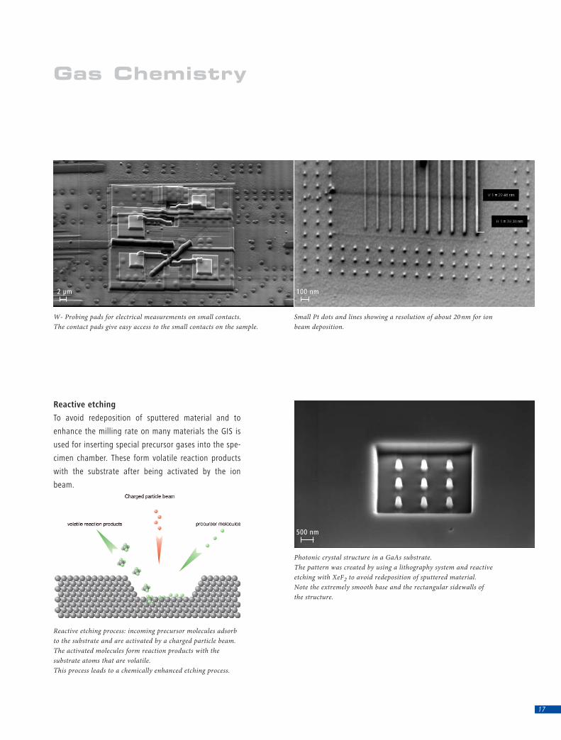
Reactive etching
To avoid redeposition of sputtered material and to
enhance the milling rate on many materials the GIS is
used for inserting special precursor gases into the spe-
cimen chamber. These form volatile reaction products
with the substrate after being activated by the ion
beam.
Gas Chemistry
Photonic crystal structure in a GaAs substrate. The pattern was created by using a lithography system and reactive etching with XeF2 to avoid redeposition of sputtered material. Note the extremely smooth base and the rectangular sidewalls of the structure.
17
Reactive etching process: incoming precursor molecules adsorb to the substrate and are activated by a charged particle beam.The activated molecules form reaction products with the substrate atoms that are volatile. This process leads to a chemically enhanced etching process.
W- Probing pads for electrical measurements on small contacts. The contact pads give easy access to the small contacts on the sample.
Small Pt dots and lines showing a resolution of about 20 nm for ionbeam deposition.
2 µm 100 nm
500 nm

Ion Beam Lithography/Micromachining
Microlens on a glass fibre surface. Structure was patterned by using a Raith Elphy Quantum lithography system. Sample courtesy of INFM Trieste.
Examples of photonic crystal structures in GaAs. The structures show perfect flat sidewalls and very high aspect ratios. To achieve the best results the structures were patterned using reactive ion milling.
For applications in the micro cosmos e.g. optical cou-
plings of micro and nano devices, photonic crystals etc.
put a high demand on micro machining capabilities.
The CrossBeam® tool is the ideal instrument to provide
micro machining and micro patterning solutions for
current and future nano scale applications.
Micro optics
If microstructures need to be connected for optical
information exchange, high precision micro optics are
needed.
Optical parameters of the micro lens:
Lens curvature: 28.5 µm, lens diameter: 10 µm; focal
length: 58.6 µm, sag height: 1.0µm; wavelength:
1550 nm.
Photonic crystals
Photonic crystals put high demands on surface rough-
ness, high aspect ratios and precise micromachining
capabilities.
Micromachined FIM tip. Sample courtesy Université de Rouen.
FIM/STM tip manufacturing
18
10 µm
2 µm
1 µm500 nm 200 nm

Nanomanipulation and Nano Probing
Micromanipulation of a TEM sample. The lamella can be easily transferred to a copper grid.
Micro probing tips approaching electrical contact pads on a microchip.
Schematic of the CrossBeam® geometry with integrated nanomanipulators.
For manipulation and probing applications (TEM Lift-
out , electrical probing etc) a set of micromanipulators
can be integrated into the CrossBeam® tool. This
converts the instrument into a nano workbench.
For electrical current measurements on small semi-
conductor devices nano probing modules are needed.
By integrating these modules into the CrossBeam® tool
measurements on a nanometre scale become possible.
Electrical measurements can be carried out even down
to the sub nA-range on microelectronics devices.
19
2 µm
10 µm

TEM Sample Preparation
20
The Lift-out technique for TEM sample preparation. The sample is thinned and cut out of the substrate. Afterwards the sample is lifted out and transferred to a TEM Grid by use of a Lift-out tool.
Metal deposition.
Final thinning until electron transparency and cut out.
Rough milling.
Final sample on TEM grid.
Final sample.
The CrossBeam® tool opens up a new dimension in TEM
sample preparation. As the sample can be imaged at
high resolution in realtime during the whole thinning
process an unsurpassed accuracy in TEM sample pre-
paration is achieved. The risk of destroying a sample
during preparation is reduced to a minimum. In additi-
on the ion milling process can be automated by using
the sophisticated automation routines provided in
SmartSEMTM.
By adding internal Lift-out tools to the CrossBeam® tool
the whole TEM preparation process can be handled
in-situ inside the vacuum of the instrument.
External Lift-out
FIB
SEM
Lift-o
ut too
l
1 µm
2 µm
1 µm
20 µm
1 µm

Geometrical position of the sample and the detectors duringion milling in the CrossBeam®.The In-lens detector is located in front of the sample andrecords information about thesample surface. The ET (Everhart-Thornley)detectector is located behind thethe sample and records SE thatare emitted from the reverseside of the sample. This signal provides informati-on about the electron transpa-rency of the sample.
Live imaging of semicon-ductor TEM sample duringion milling in split screenmode. While the In-lensdetector on the left dis-plays information about the sample surface theEverhart-Thornley detector signal on the right simultaneously provides informationabout the transparency.
In-lens Detector
SEM
FIB
ET-Detector
ee
e
e
21
In-situ Lift-out: After rough milling the tip of the Lift-out toolis welded to the lamella by using metal deposition.
The sample is cut out and lifted out of the substrate.
The lamella is transferred to a TEM grid and welded to thegrid by using the metal deposition of the GIS.
Final step: After cutting off and retracting the tip, the sample isthinned to electron transparency.
As the sample gets thinner the primary electrons start
penetrating the sample and generate secondary elec-
trons on the reverse side. These electrons can be detec-
ted by using the Everhart-Thornley detector which is
geometrically located behind the sample. This signal
gives direct information about the thickness of the
sample: The thinner the sample, the brighter the
image. At the same time the sample surface can be
imaged using the In-lens detector which is geometri-
cally located in front of the sample and collects mainly
secondary electrons which are emitted from the sample
surface. By combining both signals during the ion
milling in a split screen mode all of the sample data
(location, surface detail and thickness) can be dis-
played at the same time.
In-situ Lift-out
Copper grid
Metal depo
2 µm
2 µm 1 µm
2 µm
2 µm
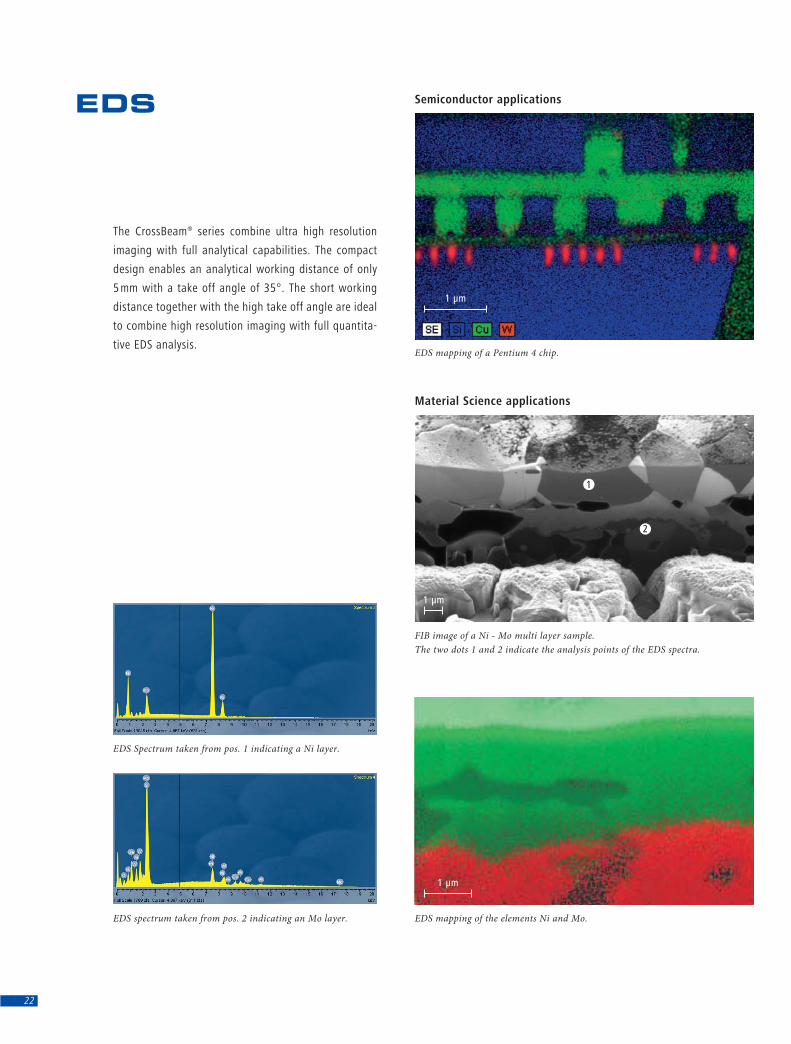
EDS
The CrossBeam® series combine ultra high resolution
imaging with full analytical capabilities. The compact
design enables an analytical working distance of only
5 mm with a take off angle of 35°. The short working
distance together with the high take off angle are ideal
to combine high resolution imaging with full quantita-
tive EDS analysis.
Semiconductor applications
Material Science applications
22
EDS mapping of a Pentium 4 chip.
FIB image of a Ni - Mo multi layer sample. The two dots 1 and 2 indicate the analysis points of the EDS spectra.
EDS mapping of the elements Ni and Mo.EDS spectrum taken from pos. 2 indicating an Mo layer.
EDS Spectrum taken from pos. 1 indicating a Ni layer.
1 µm
1 µm
1 µm
1
2

3D EBSD
EBSD is now an important tool for material characte-
rization showing the crystal structure and the texture
of polycrystalline materials in the form of crystal orien-
tation maps (COM). The CrossBeam® workstations with
a large analytical specimen chamber and the high cur-
rent GEMINI® column is ideally suited to perform EBSD.
By using the advanced image recognition and image
registration capabilities the serial process of FIB cut-
ting and EBSD Mapping can be totally automated.
Recrystallisation around a Laves-phase precipitation in a hot rol-led Fe3Al-base alloy SE-image of the microstructure.
3D Reconstruction of the Laves-phase precipitation using the orientation maps derived from the 3D image stack.
3D Image stack of orientation maps.
EBSD pattern.
Data Cortessy of S. Zaefferer, MPIE Düsseldorf, Germany
23

STEM - Scanning Transmission Electrofor the CrossBeam® Series
Microtome section of a kidney sample (STEM bright-field).
24
STEM detector assembly.
����������
���������������������
����������������������
Laser dots in a Al Ni multi layer structure (STEM bright-field).
By using a STEM (Scanning Transmission Electron Microscopy)
detector the information limit for the CrossBeam® FESEMs can
be extended beyond the nanometer range. A resolution of
0.8 nm at 30 kV is now readily attainable and gives additional
nano-scale information. The resolving power of the
CrossBeam® FESEM can be used to save processing time on
TEM systems for high resolution applications and enables high
sample throughput for quality assurance applications and
routine type measurements.
Typical application fields are:
● Materials analysis (polymer, ceramics, nanoparticles)
● Semiconductors (FIB lamellas from devices)
● Life science (histology, pathology)
The newly developed proprietary CrossBeam® Multi-Mode
STEM detection system delivers enhanced image quality by
real-time simultaneous detection of BF, DF, and orientated DF
signals, without realignment at any position.
CrossBeam® Multi-Mode STEMThe CrossBeam® Multi-Mode STEM detection system comprises
two parallel diode detector surfaces. The DF detector surface
has been divided into specific areas to allow orientated DF
imaging. The specimens are mounted in a carousel type TEM
grid holder, which holds 6 specimens. The CrossBeam® Multi-
Mode STEM detector includes a complete retractable assembly
with high precision adjustments for optimum alignment and
can be used in combination with all CrossBeam® detectors.
Advantages of the Multi-Mode STEM detector:
● Simultaneous imaging of BF and DF
● Orientated DF mode (ODF)
● STEM resolution down to 0.8 nm at 30 kV
● Ease of use with high precision positioning
● Long-life diode detector system
● Imaging of stained and unstained samples
● STEM mode EDX resolution down to 30 nm or less
2 µm
200 nm

on Microscopy
30 kV STEM image of a semiconductor sample. Bright-field (left) and dark-field (right) can be displayed simultaneously.
30 kV STEM image of W-plugs in a semiconductor device. Dark-field image (left) and ODF imaging for optimum crystallographic information (right).
25
Signal EnhancementDue to the significantly lower electron beam energies used in
the SEM, the beam-specimen interactions are much stronger.
This enables the possibility to explore subtile contrast mecha-
nisms. The STEM detector enables pure BF or DF imaging to
achieve optimum contrasts and rich imaging details of even
unstained thin sections. Furthermore it also allows EDX analy-
sis of particles down to 30 nm or less. The unique parallel STEM
detector arrangement allows simultaneous imaging and mixing
of BF, DF and orientated DF STEM signals on any position of
the TEM specimen without realignment.
The CrossBeam® Multi-Mode STEM detection system
allows the following six imaging modes:
● BF
● BF and DF added
● DF
● BF and DF subtracted
● ODF
● ODF1 and ODF2 subtracted
System ControlOperation of the CrossBeam® Multi-Mode STEM detec-
tion system and signal processing is controlled by
an additional menu embedded in the SmartSEMTM
graphical user interface.
The STEM controlenables direct selec-tion of DF, BF or ODF signal in normal orinverse mode. The STEM User modeallows user definedconfigurations to bestored and selected.
100 nm
30 nm 30 nm
100 nm

User interface
SmartSEMTM GUI for comprehensive control.
The SmartSEMTM intuitive GUI is the result of the long-
standing experience gained with software controlled
electron microscopes. Carl Zeiss SMT understands that
the quality of the result not only depends on the superb
imaging and analytical properties of the GEMINI®
FESEM column and the Canion FIB column but also on
the ease of operation of the total workstation. For the
CrossBeam® series Carl Zeiss SMT offers a dedicated
user interface for highest performance and easiest
operation.
The SmartSEMTM comprehensive GUI offers full control
over the CrossBeam® workstation with superb functio-
nality integrated into the standard package:
● Macro-Editor with access to over 250 instrument
control functions
● Automatic functions with full manual override
● Comprehensive stage control
● Full annotation and measurement capabilities
● Freely configurable toolbar
● Stage control with special mapping, stage
registration and virtual coordinate functions
Since the versatile concept of the CrossBeam® work-
stations enables a wide range of applications, the
SmartSEMTM user interface can be enhanced with
additional software modules:
● External scan and stage control for EDS
and lithography systems
● API - Advanced Programmable Interface
for full remote control
● DDE - Dynamic Data Exchange to export data
into Office applications
OPENX option for external or remote control as
part of the SmartSEMTM software philosophy enables
3rd party software to be used on the CrossBeam®
workstations or full remote control for EDS,
E-beam/Ion-beam lithography and stage navigation
applications.
26
Powerful Macro Editor with easy access to all system parameters.

27
Technical Data
CrossBeam®1540XB Essential Specifications NEON 40 CrossBeam®1560XB CrossBeam®1540EsB NEON 40EsB
Resolution SEM
Resolution FIB
Probe Current SEM
Probe Current FIB
Acceleration Voltage SEM
Acceleration Voltage FIB
Emitter SEM
Emitter FIB
Detectors In-column:
In-lens:
Chamber:
BSD:
STEM:
Specimen Chamber
Specimen Stage
Image Acquisition
Image Display
System Control
Gas Injection System
1.1 nm @ 20 kV
2.5 nm @ 1 kV
7 nm @ 30 kV guaranteed,
5 nm achievable
4 pA - 20 nA
1 pA - 50 nA
0.1 - 30 kV
2 - 30 kV
Schottky Field Emitter
Ga liquid metal ion
source (LMIS)
N/A
High Efficiency annular type (SE)
ET type (SE)
Optional solid state or scintillator type
Optional GEMINI® Multimode BF / DF detector
330 mm ø, 270 mm height
IR CCD-camera included for sample viewing
6-axes fully eucentric, all motorised
X = 102 mm, Y = 102 mm, Z = 43 mm, Z’ = 10 mm
T = -10 - 60°, R = 360° continuous
AWD (analytical working distance): 5 mm
Resolution: from 512 x 384 to 3072 x 2304 pixel, Processing: Pixel averaging, frame averaging, continuous averaging
Two 18’’ TFT monitors with image displayed at 1024 x 768 pixel
Integrated CrossBeam®/SmartSEMTM GUI based on Windows XP® operating system, controlled by mouse, control panel, keyboard and joystick
330 mm ø, 270 mm height
IR CCD-camera included for sample viewing
6-axes fully eucentric, all motorised
X = 102 mm, Y = 102 mm, Z = 43 mm, Z’ = 10 mm
T = -10 - 60°, R = 360° continuous
AWD (analytical working distance): 5 mm
EsB with filtering grid (BSE)
Filtering grid voltage 0 - 1500 V
High Efficiency annular type (SE)
ET type (SE)
Optional solid state or scintillator type
Optional GEMINI® Multimode BF / DF detector
1.1 nm @ 20 kV
2.5 nm @ 1 kV
FIB available as
upgrade
4 pA - 20 nA
FIB available as upgrade
0.1 - 30 kV
FIB optional
Schottky Field Emitter
FIB available as
upgrade
1.1 nm @ 20 kV
2.5 nm @ 1 kV
7 nm @ 30 kV guaranteed,
5 nm achievable
4 pA - 20 nA
1 pA - 50 nA
0.1 - 30 kV
2 - 30 kV
Schottky Field Emitter
Ga liquid metal ion
source (LMIS)
520 mm ø, 300 mm height
IR CCD-camera included
for sample viewing
8" large integrated airlock
210 x 50 mm
X = 152 mm, Y = 152 mm
Z = 43 mm, Z. = 10 mm
T = -15 - 65°
R = 360° continuous
1.1 nm @ 20 kV
2.5 nm @ 1 kV
7 nm @ 30 kV guaranteed,
5 nm achievable
4 pA - 20 nA
1 pA - 50 nA
0.1 - 30 kV
2 - 30 kV
Schottky Field Emitter
Ga liquid metal ion
source (LMIS)
1.1 nm @ 20 kV
2.5 nm @ 1 kV
FIB available as
upgrade
4 pA - 20 nA
FIB available as upgrade
0.1 - 30 kV
FIB optional
Schottky Field Emitter
FIB available as upgrade
Up to 5 gases for selective
etching, enhanced etching,
material deposition,
insulator deposition
GIS available as upgrade Up to 5 gases for selective
etching, enhanced etching,
material deposition,
insulator deposition
Up to 5 gases for selective
etching, enhanced etching,
material deposition,
insulator deposition
GIS available as upgrade

C a r l Z e i s s S M T – N a n o T e c h n o l o g y S y s t e m s D i v i s i o n
Due
to
a po
licy
of c
ontin
uous
dev
elop
men
t, w
e re
serv
e th
e rig
ht t
o ch
ange
spe
cific
atio
ns w
ithou
t no
tice.
Err
ors
exce
pted
. Ver
. 07-
06 ©
by
Carl
Zeis
s SM
T, O
berk
oche
n
Carl Zeiss SMT worldwide
Carl Zeiss SMT
Distributor
Global Solution Provider
The Nano Technology Systems Division of Carl Zeiss
SMT provides its customers with total solutions
featuring the latest leading-edge EM technology.
The company’s extensive know-how, meticulously
acquired over 60 years in the field of E-beam tech-
nology, has brought many pioneering innovations to
the market. Our global applications and service
network guarantees fast, reliable and high quality
support sharply focused on customer requirements.
Combined with dedicated upgrade strategies, this
will protect your investment for its entire lifetime.
The core technology embedded in our innovative
products enables us to provide solutions which add
value to our customers’ business.
Enabling the Nano-Age World®
Carl Zeiss NTS GmbH
A Carl Zeiss SMT AG Company
Carl-Zeiss-Str. 22
73447 Oberkochen
Germany
Tel. +49 73 64 / 20 44 88
Fax +49 73 64 / 20 43 43
Carl Zeiss SMT Ltd.
511 Coldhams Lane
Cambridge CB1 3JS
UK
Tel. +44 12 23 / 41 41 66
Fax +44 12 23 / 41 27 76
Carl Zeiss SMT Inc.
One Zeiss Drive, Thornwood
New York 10594
USA
Tel. +1 914 / 747 7700
Fax +1 914 / 681 7443
Carl Zeiss SMT S.a.s.
Zone d’Activité des Peupliers
27, rue des Peupliers - Bâtiment A
92000 Nanterre
France
Tel. +33 1 41 39 92 10
Fax +33 1 41 39 92 29
Plus a worldwide network
of authorised distributors
www.smt.zeiss.com/nts