
CS/EE 3700 : Fundamentals of Digital System Design Chris J. Myers Lecture 8: Synchronous Sequential...
109
CS/EE 3700 : Fundamentals of Digital System Design Chris J. Myers Lecture 8: Synchronous Sequential Circuits Chapter 8
-
Upload
anthony-malone -
Category
Documents
-
view
229 -
download
1
Transcript of CS/EE 3700 : Fundamentals of Digital System Design Chris J. Myers Lecture 8: Synchronous Sequential...
CS/EE 3700 : Fundamentals of Digital System Design
Chris J. Myers
Lecture 8: Synchronous Sequential Circuits
Chapter 8

Synchronous Sequential Circuits
• Sequential circuits – outputs depend on past behavior as well as present inputs.
• Synchronous circuits – use a clock signal to sequence behavior.
• Asynchronous circuits – no clock signal is used (see Chapter 9).
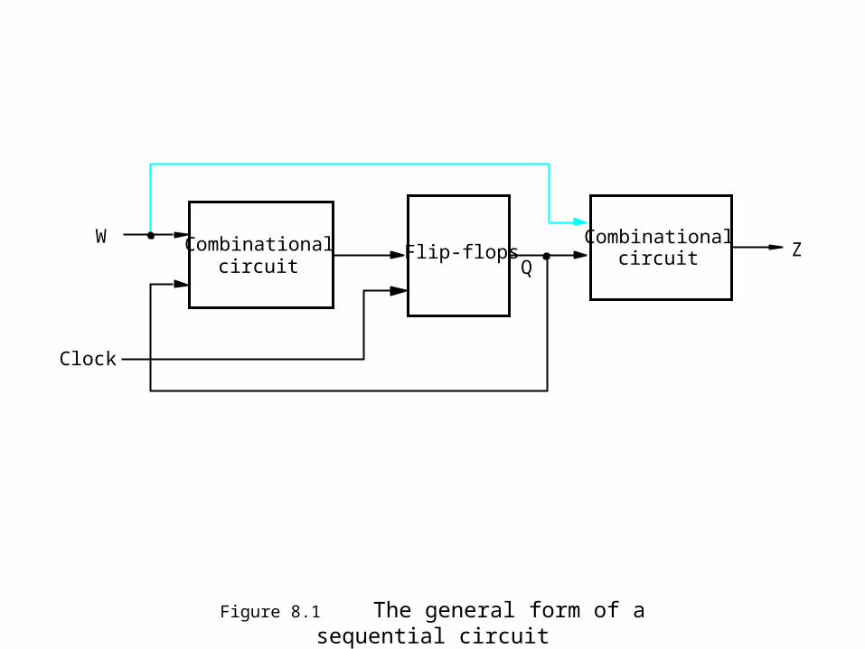
Figure 8.1 The general form of a sequential circuit
Combinational circuit
Flip-flops
Clock
Q
W Z
Combinational circuit

• Circuit has one input, w, and one output, z.
• Changes occur on positive clock edge.
• z is 1 if w is 1 during last two clock cycles.
Figure 8.2 Sequences of input and output signals
Clockcycle: t 0 t 1 t 2 t 3 t 4 t 5 t 6 t 7 t 8 t 9 t 10
w : 0 1 0 1 1 0 1 1 1 0 1 z : 0 0 0 0 0 1 0 0 1 1 0
A Simple Example

Figure 8.3 State diagram of a simple sequential circuit
C z 1 =
Reset
B z 0 = A z 0 = w 0 =
w 1 =
w 1 =
w 0 =
w 0 = w 1 =

Figure 8.4 State table
Present Next state Outputstate w = 0 w = 1 z
A A B 0 B A C 0 C A C 1

Figure 8.5 A general sequential circuit
Combinationalcircuit
Combinationalcircuit
Clock
y2
z
wy1Y1
Y2

Figure 8.6 A State-assigned table
Present Next state
state w = 0 w = 1 Output
y 2 y 1 Y 2 Y 1 Y 2 Y 1
z
A 00 00 01 0
B 01 00 10 0
C 10 00 10 1
11 dd dd d

Figure 8.7 Derivation of logic expressions
w 00 01 11 10
0
1
0
1 0
y 2
y 1
Y 1
wy 1 y 2 =
w 00 01 11 10
0
1
0 d
1 d
y 2
y 1
Y 2
wy1
y 2 wy 1 y 2
+ =
d
d
0
0
0
0
0
0
1
0 1
0
1
0
d
y 1
z y 1 y 2
= 0
1
y 2
Y 1
wy 1 y 2 =
Y 2
wy1
wy2
+ =
z y 2
=
w y 1
y 2
+ ( ) =
Ignoring don't cares Using don't cares
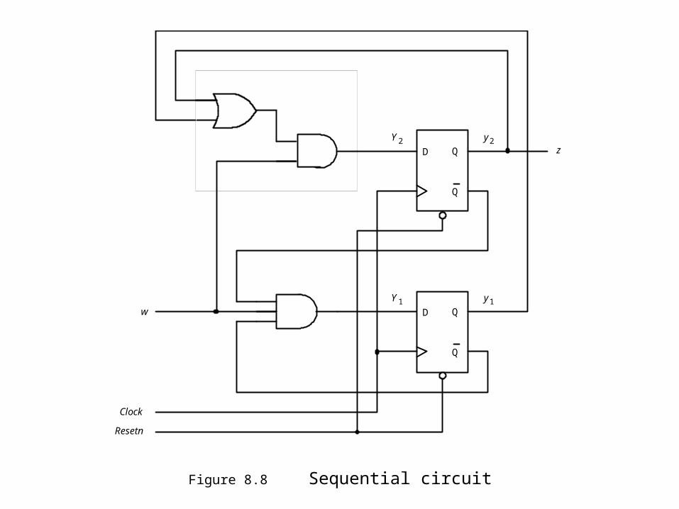
Figure 8.8 Sequential circuit
D Q
Q
D Q
Q
Y 2
Y 1 w
Clock
z
y 1
y 2
Resetn

Figure 8.9 Timing diagram
t 0 t 1 t 2 t 3 t 4 t 5 t 6 t 7 t 8 t 9 t 10
1
0
1
0
1
0
1
0
Clock
w
y 1
y 2
1
0 z

Summary of Design Steps
• Obtain specification of the desired circuit.
• Create a state diagram from specification.
• Create a state table from state diagram.
• Perform state minimization.
• Perform state assignment.
• Derive the next-state logic expressions.
• Implement circuit described by logic.

Figure 7.56 A digital system with k registers
R 1 in Rk in
Bus
Clock
R 1 out R 2 in R 2 out Rkout
Control circuit Function
R 1 R 2 Rk
Data
Extern

Figure 7.58 A shift-register control circuit
D Q
Q Clock
D Q
Q
D Q
Q
w
R 2 out R 3 in
Reset
R 1 out R 2 in R 3 out R 1 in

Figure 8.10 Signals needed in Example 8.1
Control circuit
w
Clock
Done
R 1 out
R 2 out
R 1 in
R 2 inR 3 out R 3 in

Figure 8.11 State diagram
D R 3 out 1 = R 1 in 1 = Done 1 =
w 0 = w 1 =
C R 1 out 1 = R 2 in 1 =
B R 2 out 1 = R 3 in 1 =
w 1 =
A No
w 0 = w 1 =
transfer
w 0 = w 1 =
Reset
w 0 =
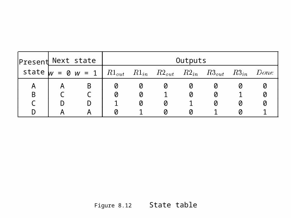
Figure 8.12 State table
Present Next state Outputs
state
A A B 0 0 0 0 0 0 0 B C C 0 0 1 0 0 1 0 C D D 1 0 0 1 0 0 0 D A A 0 1 0 0 1 0 1
w = 0 w = 1

Figure 8.13 State-assigned table
Present Nextstate
state Outputs
A 00 00 0 1 0 0 0 0 0 0 0 B 01 10 1 0 0 0 1 0 0 1 0 C 10 11 1 1 1 0 0 1 0 0 0 D 11 00 0 0 0 1 0 0 1 0 1
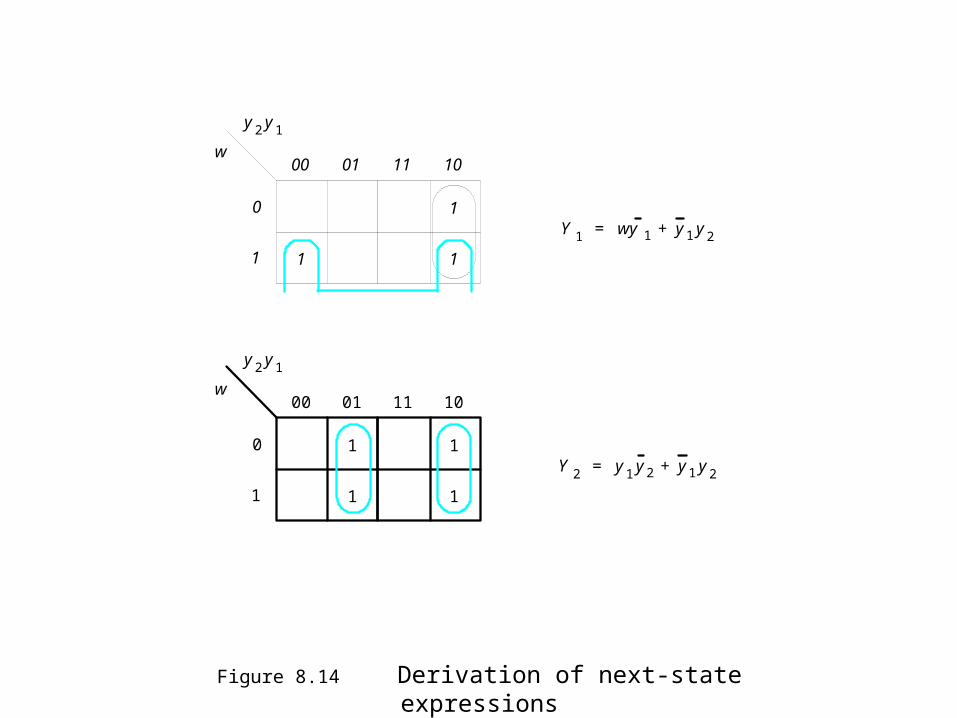
Figure 8.14 Derivation of next-state expressions
w 00 01 11 10
0
1
1
1 1
y 2 y 1
Y 1 wy1 y 1 y 2 + =
w 00 01 11 10
0
1
1 1
1 1
y 2 y 1
Y 2 y 1 y 2 y 1 y 2 + =
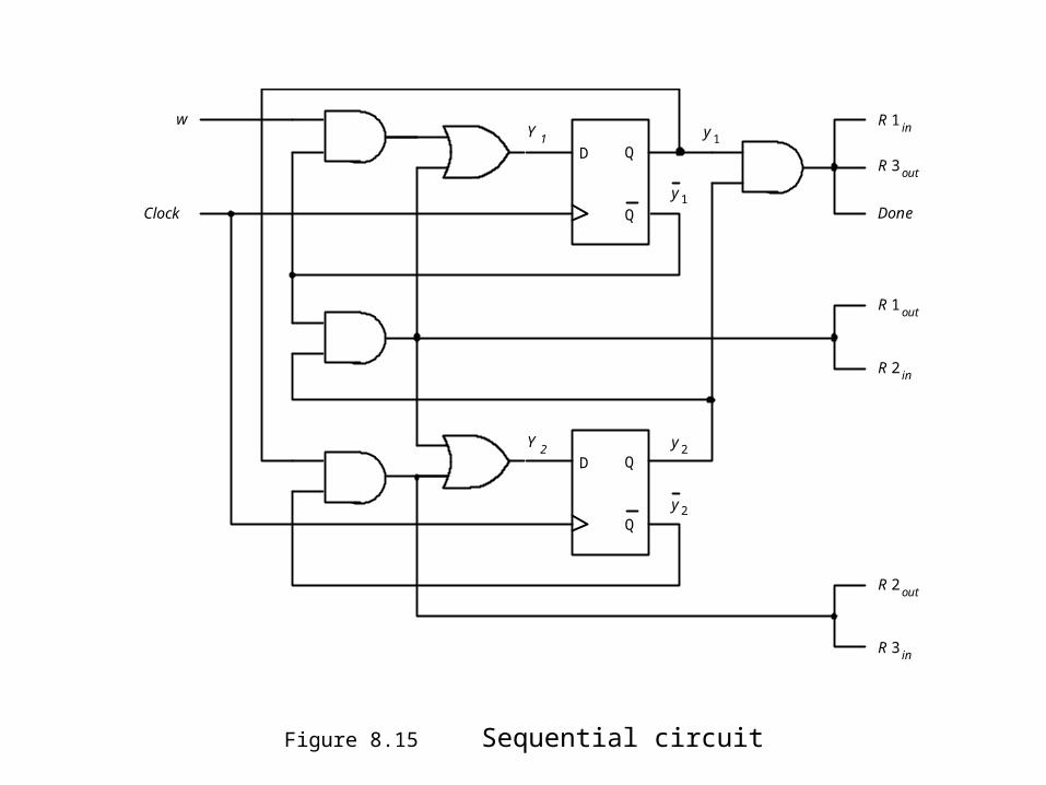
Figure 8.15 Sequential circuit
D Q
Q
D Q
Q
Done
w
Clock
Y 2
Y 1
y 2
y 1
y 2
y 1
R 1 in
R 3 out
R 1 out
R 2 in
R 2 out
R 3 in
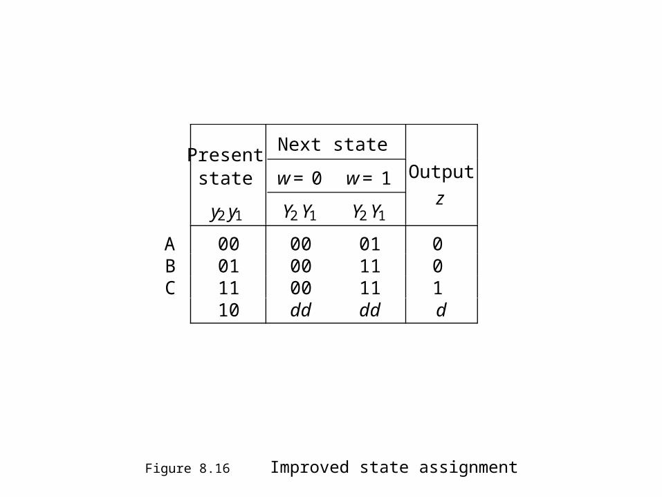
Figure 8.16 Improved state assignment
Present Next state
state w = 0 w = 1 Output
y 2 y 1 Y 2 Y 1 Y 2 Y 1 z
A 00 00 01 0 B 01 00 11 0 C 11 00 11 1
10 dd dd d
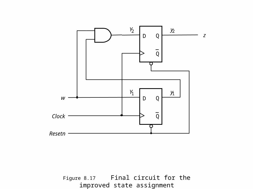
Figure 8.17 Final circuit for the improved state assignment
D Q
Q
D Q
Q
Y 2
Y 1 w
Clock
z
y 1
y 2
Resetn
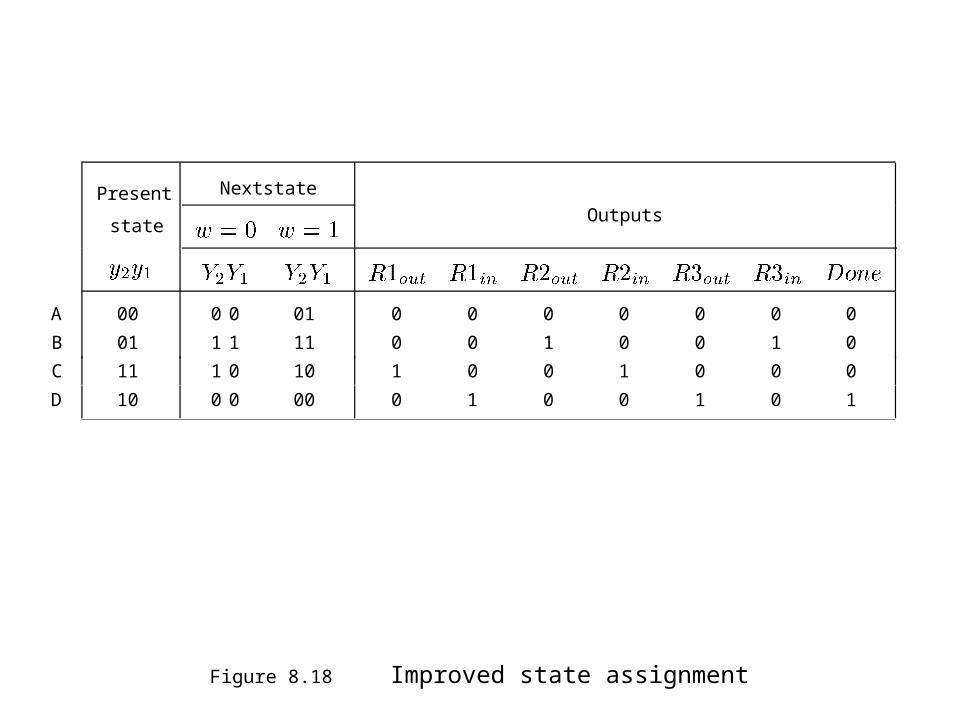
Figure 8.18 Improved state assignment
Present Nextstate
state Outputs
A 00 0 0 01 0 0 0 0 0 0 0 B 01 1 1 11 0 0 1 0 0 1 0 C 11 1 0 10 1 0 0 1 0 0 0 D 10 0 0 00 0 1 0 0 1 0 1
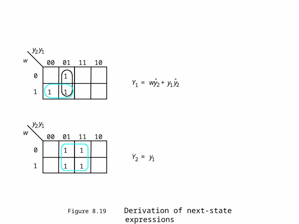
Figure 8.19 Derivation of next-state expressions
w 00 01 11 10
0
1
1
1 1
y 2 y 1
Y 1 wy2 y 1 y 2 + =
w 00 01 11 10
0
1
1 1
1 1
y 2 y 1
Y 2 y 1 =
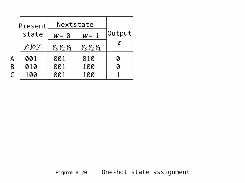
Figure 8.20 One-hot state assignment
Present Nextstate
state w = 0 w = 1 Output
y 3 y 2 y 1 Y 3 Y 2 Y 1 Y 3 Y 2 Y 1 z
A 001 001 010 0 B 010 001 100 0 C 100 001 100 1
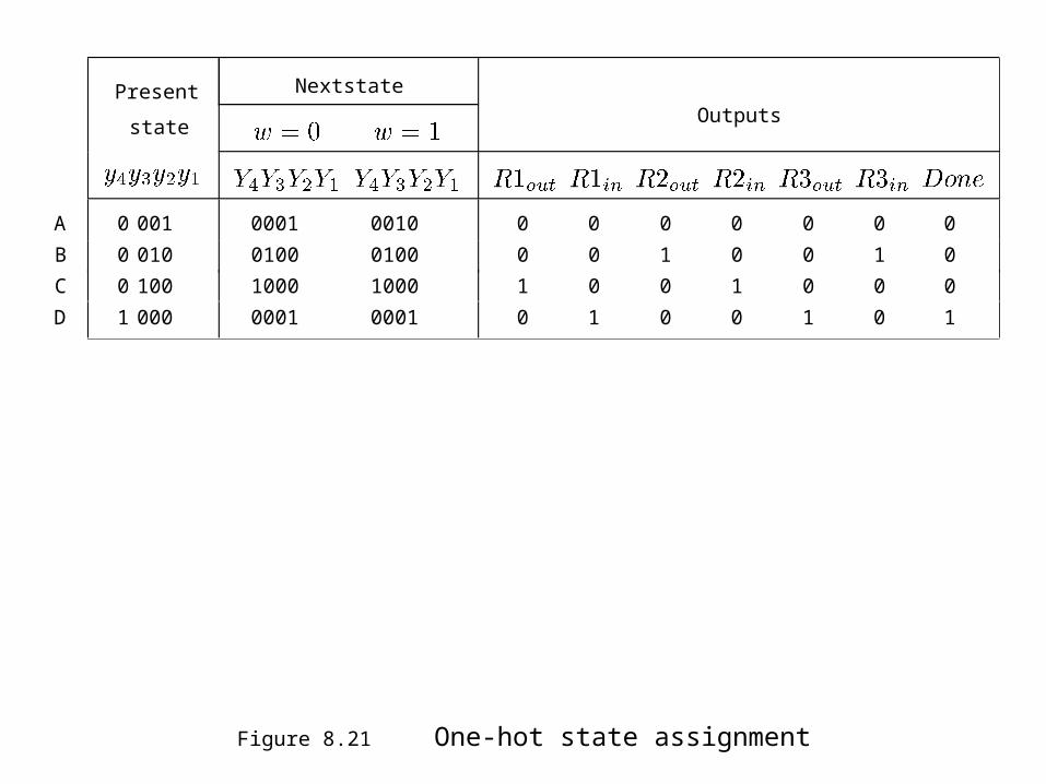
Figure 8.21 One-hot state assignment
Present Nextstate
state Outputs
A 0 001 0001 0010 0 0 0 0 0 0 0 B 0 010 0100 0100 0 0 1 0 0 1 0 C 0 100 1000 1000 1 0 0 1 0 0 0 D 1 000 0001 0001 0 1 0 0 1 0 1
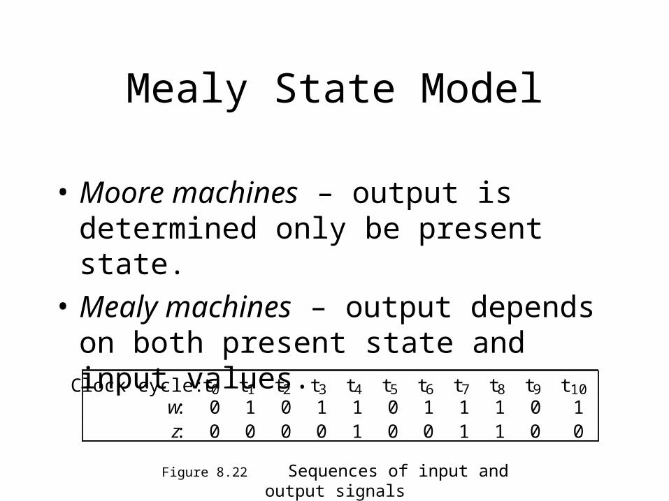
Figure 8.22 Sequences of input and output signals
Clock cycle: t 0 t 1 t 2 t 3 t 4 t 5 t 6 t 7 t 8 t 9 t 10
w : 0 1 0 1 1 0 1 1 1 0 1 z : 0 0 0 0 1 0 0 1 1 0 0
Mealy State Model
• Moore machines – output is determined only be present state.
• Mealy machines – output depends on both present state and input values.
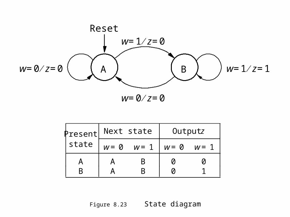
Figure 8.23 State diagram
A
w 0 = z 0 =
w 1 = z 1 = B w 0 = z 0 =
Reset w 1 = z 0 =
Present Next state Output z
state w = 0 w = 1 w = 0 w = 1
A A B 0 0 B A B 0 1

Figure 8.24 State table
Present Next state Output z
state w = 0 w = 1 w = 0 w = 1
A A B 0 0 B A B 0 1
Present Next state Output
state w = 0 w = 1 w = 0 w = 1
y Y Y z z
A 0 0 1 0 0 B 1 0 1 0 1

Figure 8.26 FSM implementation
Clock
Resetn
D Q
Q
w
z
(a) Circuit
t 0 t 1 t 2 t 3 t 4 t 5 t 6 t 7 t 8 t 9 t 101 0
1 0
1 0
1 0
Clock
y
w
z
y
(b) Timing diagram

Figure 8.27 FSM implementation
Clock
Resetn
D Q
Q
w
z
(a) Circuit
t 0 t 1 t 2 t 3 t 4 t 5 t 6 t 7 t 8 t 9 t 101
0
1
0
1
0
1
0
Clock
y
w
z
y
(b) Timing diagram
D Q
Q
Z
1
0 Z

Figure 8.28 State diagram for Example 8.4
R3out 1= R1in 1= Done 1= w 0=w 1=
R1out 1= R2in 1=
w 1= R 2out 1= R3in 1=
A
w 0=w 1=
Reset
w 0=
B
C

Figure 7.59 A modified control circuit
D Q
Q Clock
D Q
Q
D Q
Q
w
R 2 out R 3 in R 1 out R 2 in R 3 out R 1 in
P
Reset
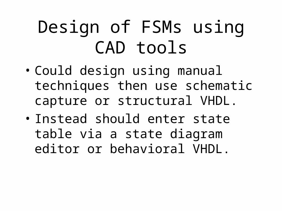
Design of FSMs using CAD tools
• Could design using manual techniques then use schematic capture or structural VHDL.
• Instead should enter state table via a state diagram editor or behavioral VHDL.
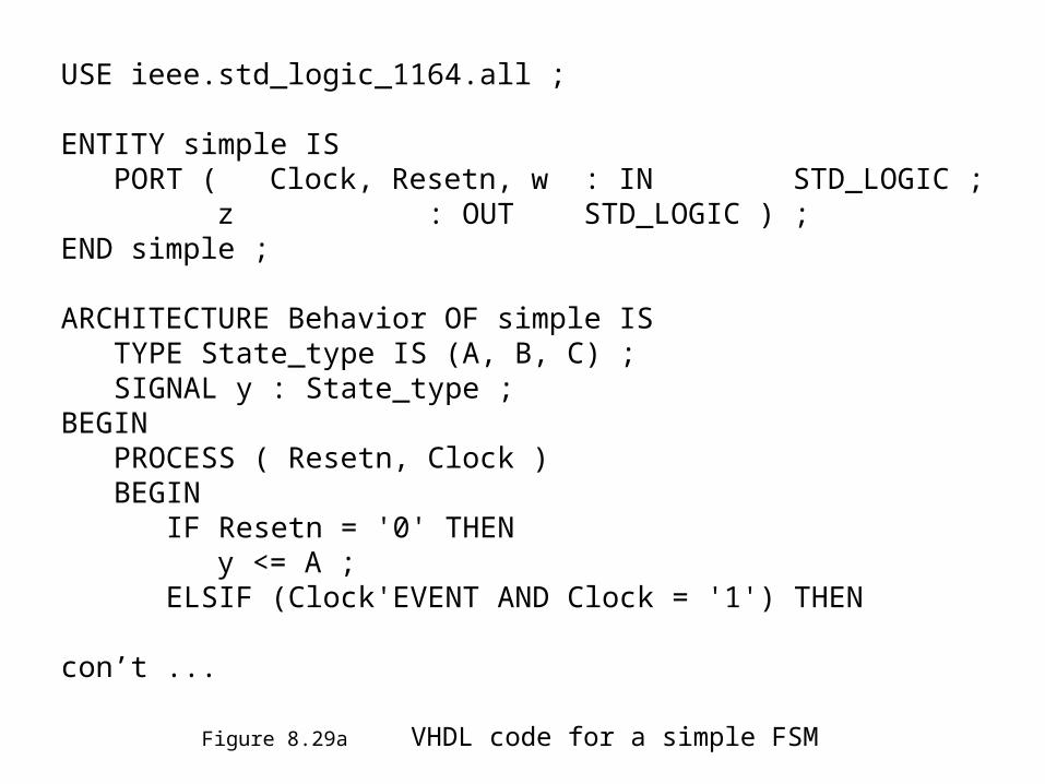
Figure 8.29a VHDL code for a simple FSM
USE ieee.std_logic_1164.all ;
ENTITY simple ISPORT ( Clock, Resetn, w : IN STD_LOGIC ;
z : OUT STD_LOGIC ) ;END simple ;
ARCHITECTURE Behavior OF simple ISTYPE State_type IS (A, B, C) ;SIGNAL y : State_type ;
BEGINPROCESS ( Resetn, Clock )BEGIN
IF Resetn = '0' THENy <= A ;
ELSIF (Clock'EVENT AND Clock = '1') THEN
con’t ...
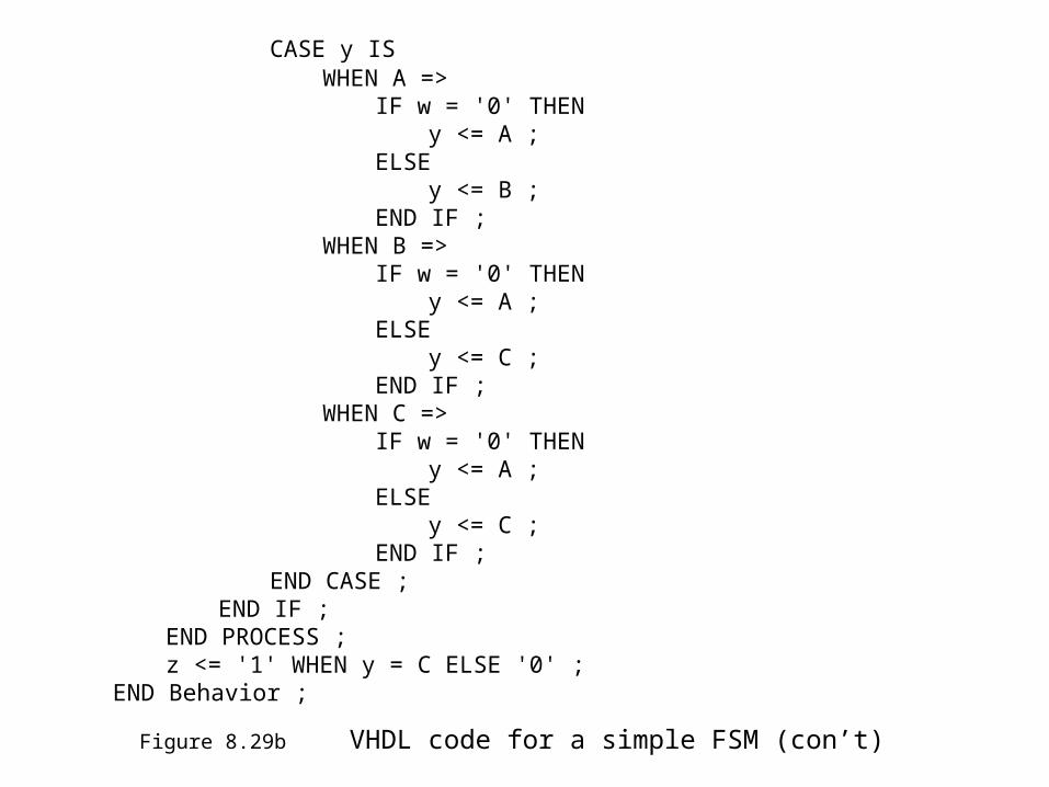
CASE y ISWHEN A =>
IF w = '0' THENy <= A ;
ELSEy <= B ;
END IF ;WHEN B =>
IF w = '0' THENy <= A ;
ELSEy <= C ;
END IF ;WHEN C =>
IF w = '0' THENy <= A ;
ELSEy <= C ;
END IF ;END CASE ;
END IF ;END PROCESS ;z <= '1' WHEN y = C ELSE '0' ;
END Behavior ;
Figure 8.29b VHDL code for a simple FSM (con’t)

Figure 8.30 Implementation of an FSM in a CPLD
y1D Q
D Q
Clock
1
11
PAL-like block
Interconnection wires
(Other macrocells are not shown)
1
0
0
D Q
100 z
w
Resetn
y2

Figure 8.31 An FSM circuit in a small CPLD
EPM7032
z
Rese
tn
w
Clo
ck
Gn
d
V D
D
1 4 7
10
13
1619 22 25 28
44 39
36

Figure 8.32 Simulation results
(a) Timing simulation results
(b) Magnified simulation results, showing timing details

(ENTITY declaration not shown)
ARCHITECTURE Behavior OF simple ISTYPE State_type IS (A, B, C) ;SIGNAL y_present, y_next : State_type ;
BEGINPROCESS ( w, y_present )BEGIN
CASE y_present ISWHEN A =>
IF w = '0' THENy_next <= A ;
ELSEy_next <= B ;
END IF ;WHEN B =>
IF w = '0' THENy_next <= A ;
ELSEy_next <= C ;
END IF ;
Figure 8.33a Alternative style of code for an FSM

WHEN C =>IF w = '0' THEN
y_next <= A ;ELSE
y_next <= C ;END IF ;
END CASE ;END PROCESS ;
PROCESS (Clock, Resetn)BEGIN
IF Resetn = '0' THENy_present <= A ;
ELSIF (Clock'EVENT AND Clock = '1') THENy_present <= y_next ;
END IF ;END PROCESS ;
z <= '1' WHEN y_present = C ELSE '0' ;END Behavior ;
Figure 8.33b Alternative style of code for an FSM (con’t)
(ENTITY declaration not shown)
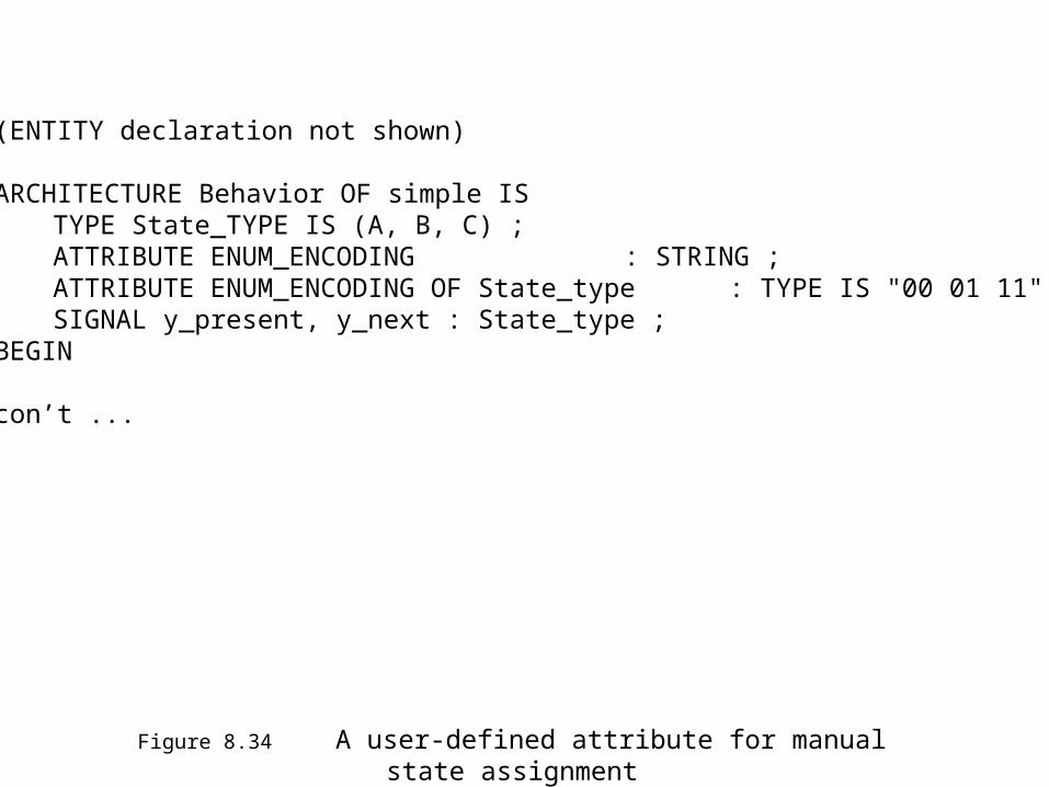
ARCHITECTURE Behavior OF simple ISTYPE State_TYPE IS (A, B, C) ;ATTRIBUTE ENUM_ENCODING : STRING ;ATTRIBUTE ENUM_ENCODING OF State_type : TYPE IS "00 01 11" ;SIGNAL y_present, y_next : State_type ;
BEGIN
con’t ...
Figure 8.34 A user-defined attribute for manual state assignment
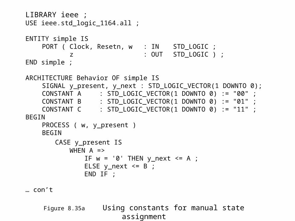
Figure 8.35a Using constants for manual state assignment
LIBRARY ieee ;USE ieee.std_logic_1164.all ;
ENTITY simple ISPORT ( Clock, Resetn, w : IN STD_LOGIC ;
z : OUT STD_LOGIC ) ;END simple ;
ARCHITECTURE Behavior OF simple ISSIGNAL y_present, y_next : STD_LOGIC_VECTOR(1 DOWNTO 0);CONSTANT A : STD_LOGIC_VECTOR(1 DOWNTO 0) := "00" ;CONSTANT B : STD_LOGIC_VECTOR(1 DOWNTO 0) := "01" ;CONSTANT C : STD_LOGIC_VECTOR(1 DOWNTO 0) := "11" ;
BEGINPROCESS ( w, y_present )BEGIN
CASE y_present ISWHEN A =>
IF w = '0' THEN y_next <= A ;ELSE y_next <= B ;END IF ;
… con’t
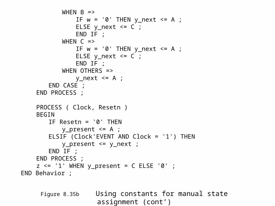
Figure 8.35b Using constants for manual state assignment (cont’)
WHEN B =>IF w = '0' THEN y_next <= A ;ELSE y_next <= C ;END IF ;
WHEN C =>IF w = '0' THEN y_next <= A ;ELSE y_next <= C ;END IF ;
WHEN OTHERS =>y_next <= A ;
END CASE ;END PROCESS ;
PROCESS ( Clock, Resetn )BEGIN
IF Resetn = '0' THENy_present <= A ;
ELSIF (Clock'EVENT AND Clock = '1') THENy_present <= y_next ;
END IF ;END PROCESS ;z <= '1' WHEN y_present = C ELSE '0' ;
END Behavior ;
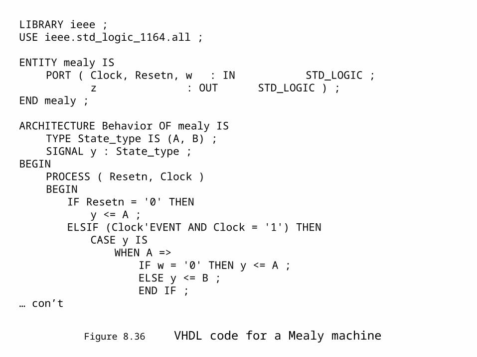
Figure 8.36 VHDL code for a Mealy machine
LIBRARY ieee ;USE ieee.std_logic_1164.all ;
ENTITY mealy ISPORT ( Clock, Resetn, w : IN STD_LOGIC ;
z : OUT STD_LOGIC ) ;END mealy ;
ARCHITECTURE Behavior OF mealy ISTYPE State_type IS (A, B) ;SIGNAL y : State_type ;
BEGINPROCESS ( Resetn, Clock )BEGIN
IF Resetn = '0' THENy <= A ;
ELSIF (Clock'EVENT AND Clock = '1') THENCASE y IS
WHEN A =>IF w = '0' THEN y <= A ;ELSE y <= B ;END IF ;
… con’t
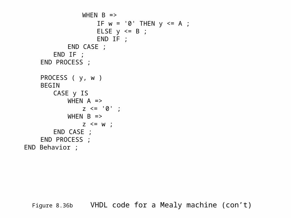
Figure 8.36b VHDL code for a Mealy machine (con’t)
WHEN B =>IF w = '0' THEN y <= A ;ELSE y <= B ;END IF ;
END CASE ;END IF ;
END PROCESS ;
PROCESS ( y, w )BEGIN
CASE y ISWHEN A =>
z <= '0' ;WHEN B =>
z <= w ;END CASE ;
END PROCESS ;END Behavior ;

Figure 8.37 Simulation results for the Mealy machine

Figure 8.38 Potential problem with asynchronous inputs to a Mealy FSM
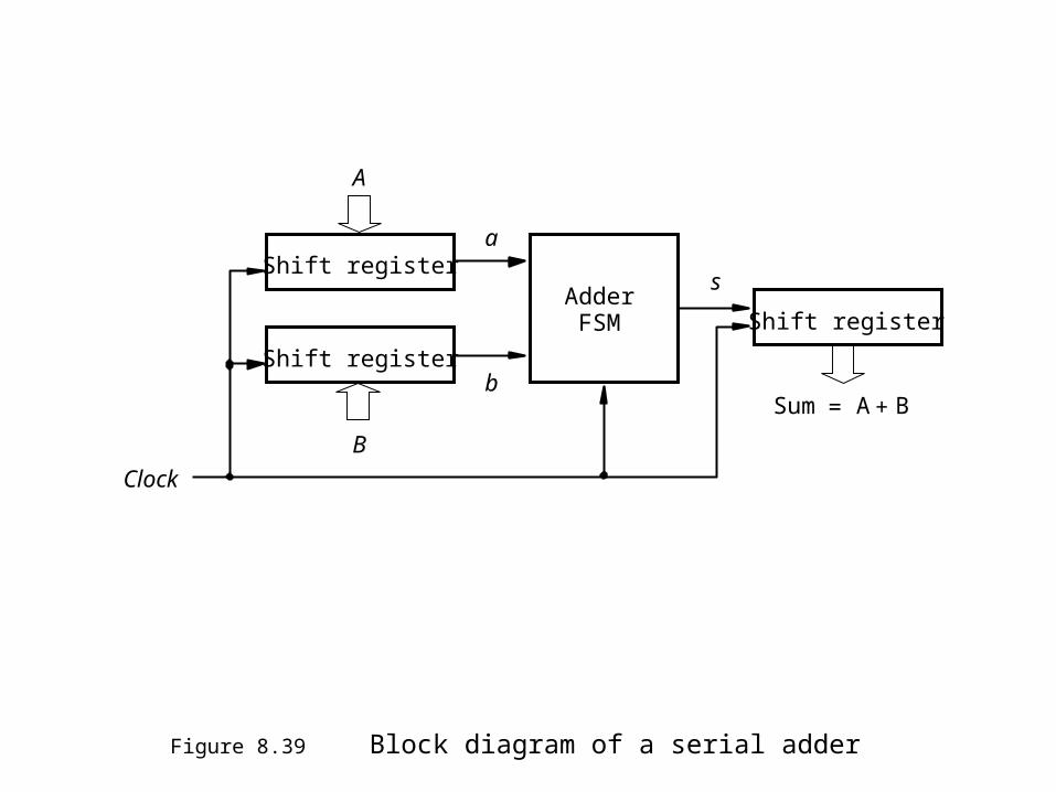
Figure 8.39 Block diagram of a serial adder
Sum A B + =
Shift register
Shift register
Adder FSM Shift register
B
A
a
b
s
Clock
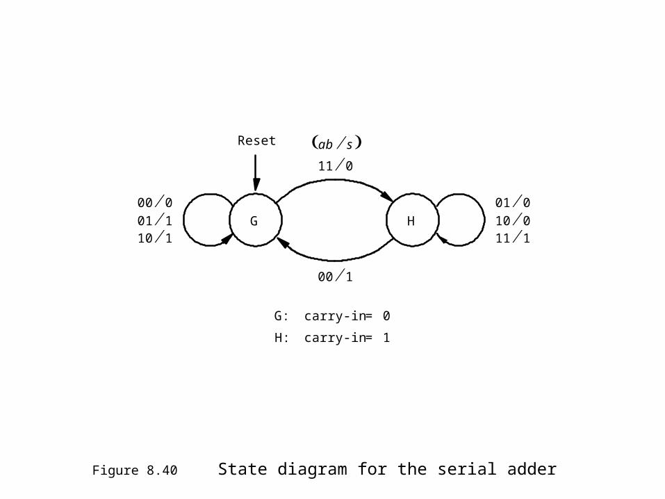
Figure 8.40 State diagram for the serial adder
G
00 1
11 1 10 0 01 0
H 10 1 01 1 00 0
carry-in 0 =
carry-in 1 = G:
H:
Reset
11 0 ab s
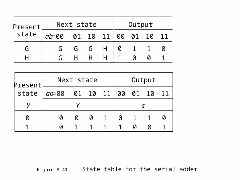
Figure 8.41 State table for the serial adder
Present Next state Output s
state ab =00 01 10 11 00 01 10 11
G G G G H 0 1 1 0 H G H H H 1 0 0 1
Present Next state Output
state ab =00 01 10 11 00 01 10 11
y Y s
0 0 0 0 1 0 1 1 0 1 0 1 1 1 1 0 0 1

Figure 8.43 Circuit for the adder FSM
Fulladder
a
b
s
D Q
Q
carry-out
Clock
Reset
Y y
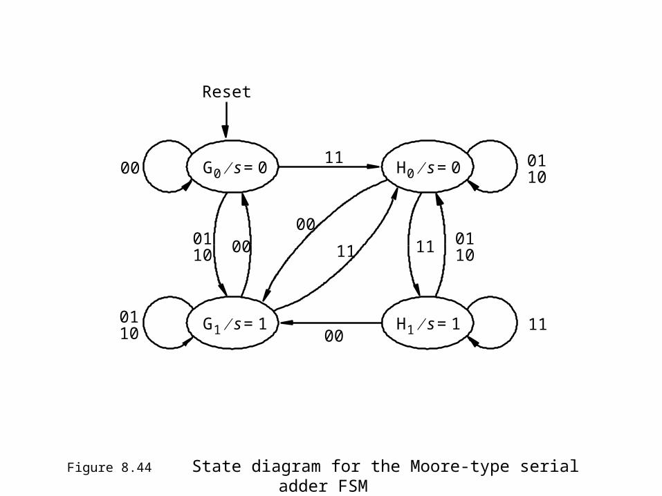
Figure 8.44 State diagram for the Moore-type serial adder FSM
H 1 s 1 =
Reset
H 0 s 0 =
011011
11
0110
G 1 s 1 =
G 0 s 0 =
0110 00
01
00
10
11
00
00
11
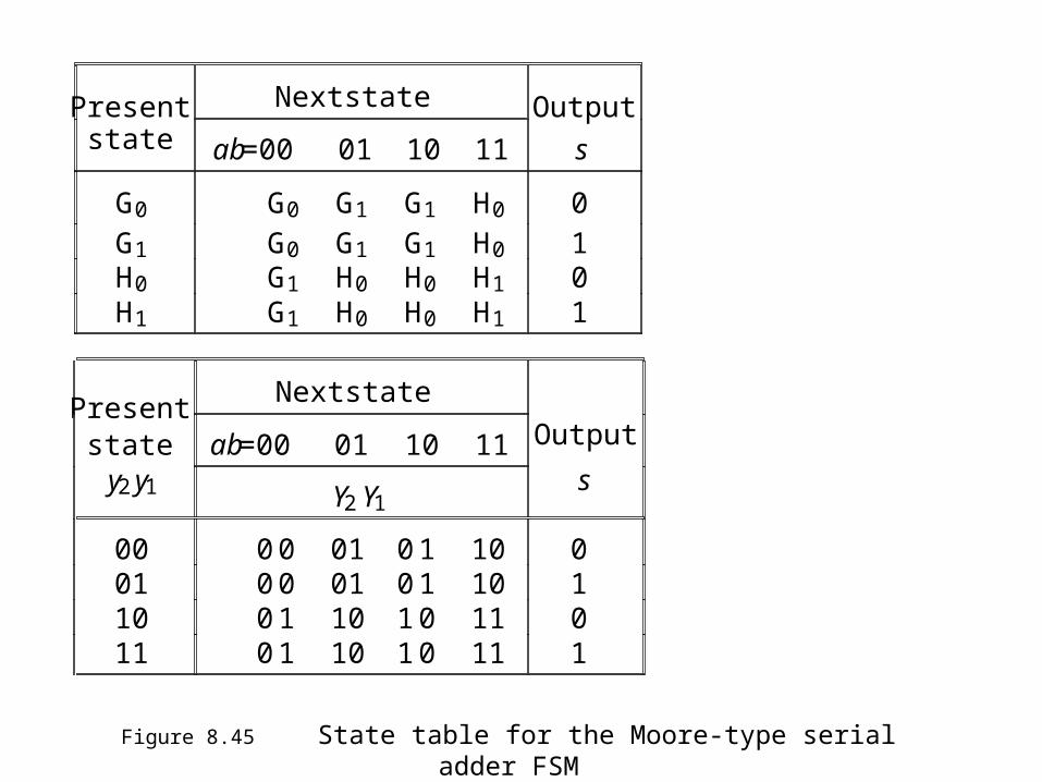
Figure 8.45 State table for the Moore-type serial adder FSM
Present Nextstate Outputstate ab =00 01 10 11 s
G 0 G 0 G 1 G 1 H 0 0 G 1 G 0 G 1 G 1 H 0 1 H 0 G 1 H 0 H 0 H 1 0 H 1 G 1 H 0 H 0 H 1 1
Present Nextstate
state ab =00 01 10 11 Output
y 2 y 1 Y 2 Y 1 s
00 0 0 01 0 1 10 0 01 0 0 01 0 1 10 1 10 0 1 10 1 0 11 0 11 0 1 10 1 0 11 1

Figure 8.47 Circuit for the Moore-type serial adder FSM
Fulladder
a
b
D Q
Q Carry-out
Clock
Reset
D Q
Q
s
Y 2
Y 1 Sum bit
y 2
y 1
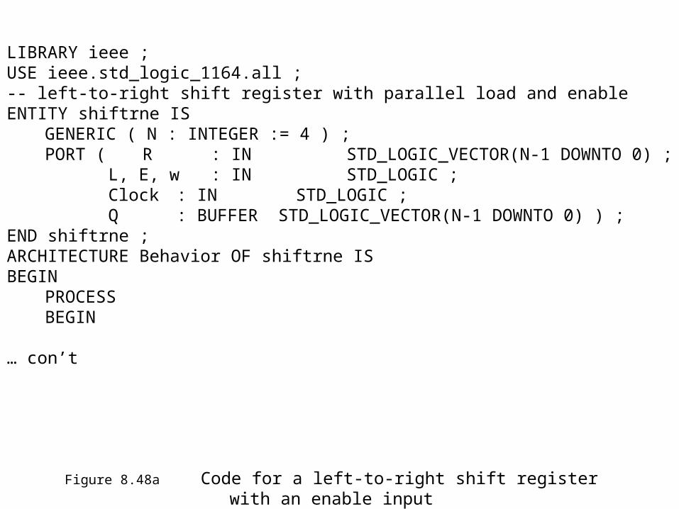
Figure 8.48a Code for a left-to-right shift register with an enable input
LIBRARY ieee ;USE ieee.std_logic_1164.all ;-- left-to-right shift register with parallel load and enableENTITY shiftrne IS
GENERIC ( N : INTEGER := 4 ) ;PORT ( R : IN STD_LOGIC_VECTOR(N-1 DOWNTO 0) ;
L, E, w : IN STD_LOGIC ;Clock : IN STD_LOGIC ;Q : BUFFER STD_LOGIC_VECTOR(N-1 DOWNTO 0) ) ;
END shiftrne ;ARCHITECTURE Behavior OF shiftrne ISBEGIN
PROCESSBEGIN
… con’t
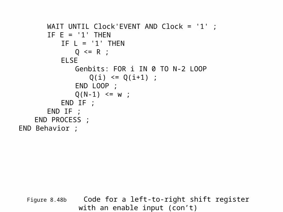
WAIT UNTIL Clock'EVENT AND Clock = '1' ;IF E = '1' THEN
IF L = '1' THENQ <= R ;
ELSEGenbits: FOR i IN 0 TO N-2 LOOP
Q(i) <= Q(i+1) ;END LOOP ;Q(N-1) <= w ;
END IF ;END IF ;
END PROCESS ;END Behavior ;
Figure 8.48b Code for a left-to-right shift register with an enable input (con’t)

Figure 8.49a VHDL code for the serial adder
LIBRARY ieee ;USE ieee.std_logic_1164.all ;ENTITY serial IS
GENERIC ( length : INTEGER := 8 ) ;PORT ( Clock : IN STD_LOGIC ;
Reset : IN STD_LOGIC ;A, B : IN STD_LOGIC_VECTOR(length-1 DOWNTO 0) ;Sum : BUFFER STD_LOGIC_VECTOR(length-1 DOWNTO 0) );
END serial ;
ARCHITECTURE Behavior OF serial ISCOMPONENT shiftrne
GENERIC ( N : INTEGER := 4 ) ;PORT ( R : IN STD_LOGIC_VECTOR(N-1 DOWNTO 0) ;
L, E, w : IN STD_LOGIC ;Clock : IN STD_LOGIC ;Q : BUFFER STD_LOGIC_VECTOR(N-1 DOWNTO 0) ) ;
END COMPONENT ;SIGNAL QA, QB, Null_in : STD_LOGIC_VECTOR(length-1 DOWNTO 0) ;SIGNAL s, Low, High, Run : STD_LOGIC ;SIGNAL Count : INTEGER RANGE 0 TO length ;TYPE State_type IS (G, H) ;SIGNAL y : State_type ;
… con’t
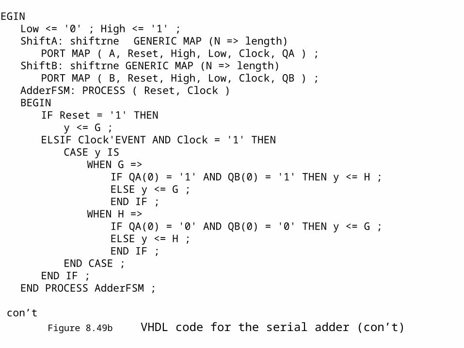
Figure 8.49b VHDL code for the serial adder (con’t)
BEGINLow <= '0' ; High <= '1' ;ShiftA: shiftrne GENERIC MAP (N => length)
PORT MAP ( A, Reset, High, Low, Clock, QA ) ;ShiftB: shiftrne GENERIC MAP (N => length)
PORT MAP ( B, Reset, High, Low, Clock, QB ) ;AdderFSM: PROCESS ( Reset, Clock )BEGIN
IF Reset = '1' THENy <= G ;
ELSIF Clock'EVENT AND Clock = '1' THENCASE y IS
WHEN G =>IF QA(0) = '1' AND QB(0) = '1' THEN y <= H ;ELSE y <= G ;END IF ;
WHEN H =>IF QA(0) = '0' AND QB(0) = '0' THEN y <= G ;ELSE y <= H ;END IF ;
END CASE ;END IF ;
END PROCESS AdderFSM ;
… con’t

Figure 8.49c VHDL code for the serial adder (con’t)
WITH y SELECTs <= QA(0) XOR QB(0) WHEN G,
NOT ( QA(0) XOR QB(0) ) WHEN H ;Null_in <= (OTHERS => '0') ;ShiftSum: shiftrne GENERIC MAP ( N => length )
PORT MAP ( Null_in, Reset, Run, s, Clock, Sum ) ;Stop: PROCESSBEGIN
WAIT UNTIL (Clock'EVENT AND Clock = '1') ;IF Reset = '1' THEN
Count <= length ;ELSIF Run = '1' THEN
Count <= Count -1 ;END IF ;
END PROCESS ;Run <= '0' WHEN Count = 0 ELSE '1' ; -- stops counter and ShiftSum
END Behavior ;
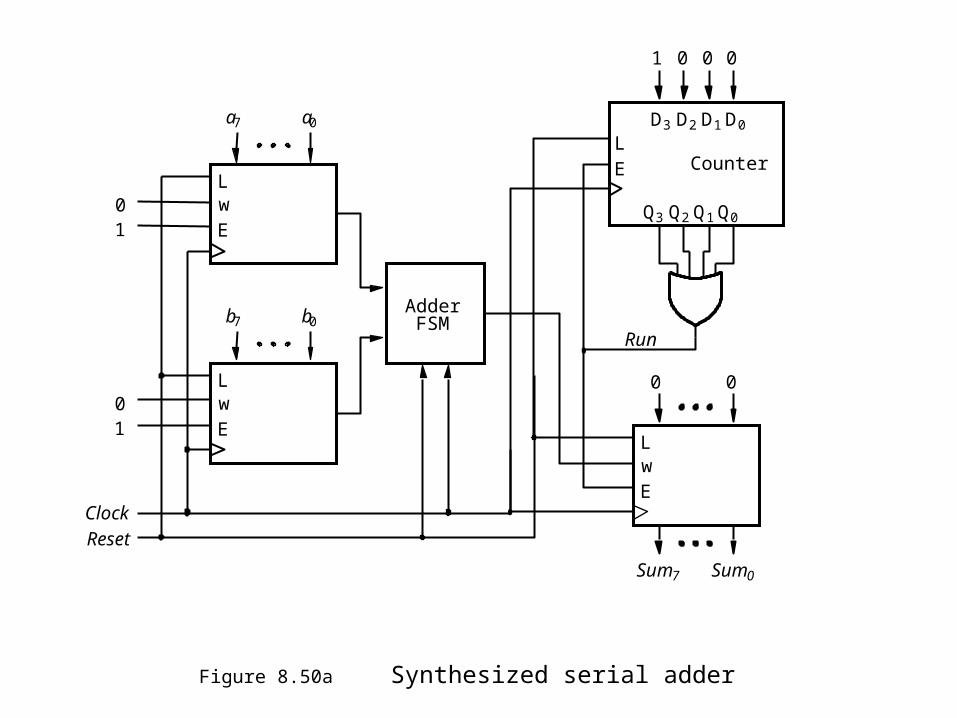
Figure 8.50a Synthesized serial adder
Adder FSM
Clock
E w L
E w L
b 7 b 0
a 7 a 0
E w L
E L
Q 3 Q 2 Q 1 Q 0
D 3 D 2 D 1 D 0
1 0 0 0
Counter
0 0
Reset
Sum 7 Sum 0
0 1
0 1
Run

Figure 8.50b Simulation results for the synthesized serial adder

State Minimization
• It is often difficult for designer to find FSM with minimal number of states.
• Fewer states leads to fewer flip-flops.
• Two states Si and Sj are equivalent iff for every input sequence starting in Si or Sj, the same output sequence is produced.
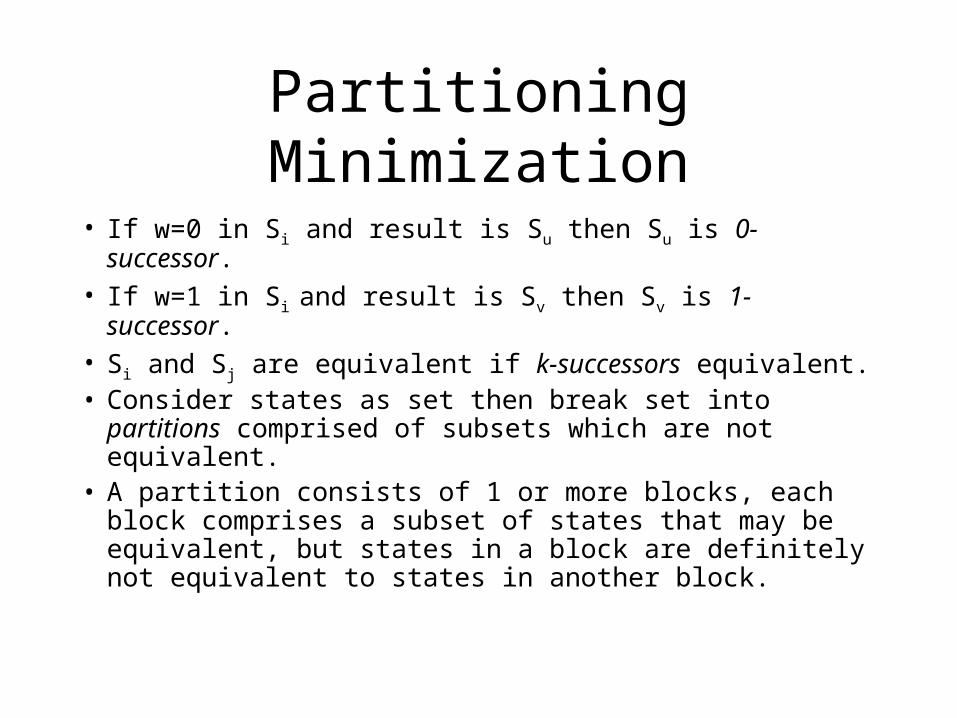
Partitioning Minimization
• If w=0 in Si and result is Su then Su is 0-successor.• If w=1 in Si and result is Sv then Sv is 1-successor.• Si and Sj are equivalent if k-successors equivalent.• Consider states as set then break set into partitions
comprised of subsets which are not equivalent.• A partition consists of 1 or more blocks, each
block comprises a subset of states that may be equivalent, but states in a block are definitely not equivalent to states in another block.

Figure 8.51 State table for Example 8.5
Present Next state Outputstate w = 0 w = 1 z
A B C 1 B D F 1 C F E 0 D B G 1 E F C 0 F E D 0 G F G 0

Figure 8.52 Minimized state table for Example 8.5
Present Nextstate Outputstate w = 0 w = 1 z
A B C 1 B A F 1 C F C 0 F C A 0

Figure 8.53 Signals for the vending machine
D Q
Q
sense N D Q
Q Clock
N
sense N
sense D
Clock
N
D
(a) Timing diagram
(b) Circuit that generates N
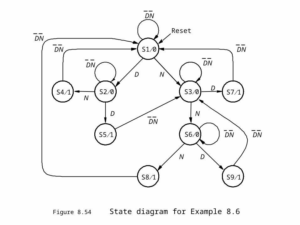
Figure 8.54 State diagram for Example 8.6
S1 0
S7 1
DN
D N
S3 0
S6 0
S9 1 S8 1
S2 0
S5 1
S4 1
DNDN
DNDN
DN
DN
DN
D
D N
D N
DN
N
Reset

Figure 8.55 State table for Example 8.6
Present Next state Outputstate DN =00 01 10 11 z
S1 S1 S3 S2 0 S2 S2 S4 S5 0 S3 S3 S6 S7 0 S4 S1 1 S5 S3 1 S6 S6 S8 S9 0 S7 S1 1 S8 S1 1 S9 S3 1
––
–––
––
–––
–––––––––

Figure 8.56 Minimized state table for Example 8.6
Present Next state Outputstate DN =00 01 10 11 z
S1 S1 S3 S2 0 S2 S2 S4 S5 0 S3 S3 S2 S4 0 S4 S1 1 S5 S3 1
–––
– – –– – –

Figure 8.57 Minimized state diagram for Example 8.6
S1 0
S5 1
DNDN
DN
DN
DN
D
D
D
N
N
N
S3 0
S2 0
S4 1
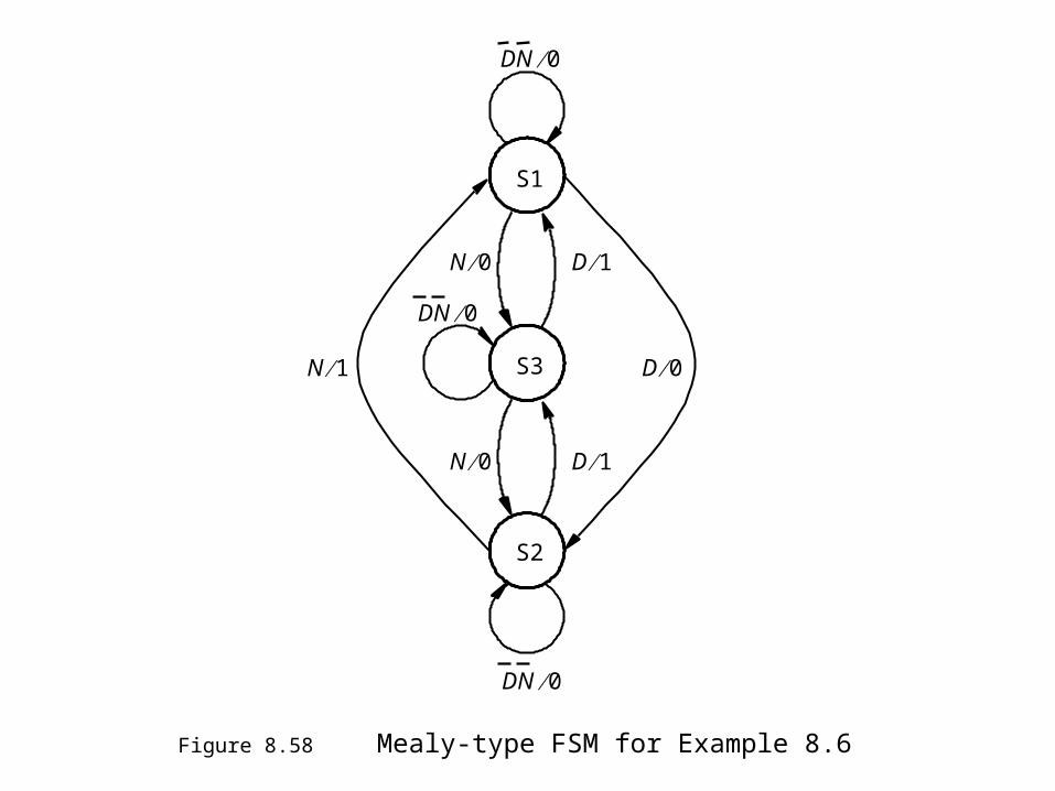
Figure 8.58 Mealy-type FSM for Example 8.6
S3
S2
D 0
S1
D 1
D 1
N 1
N 0
N 0
DN 0
DN 0
DN 0
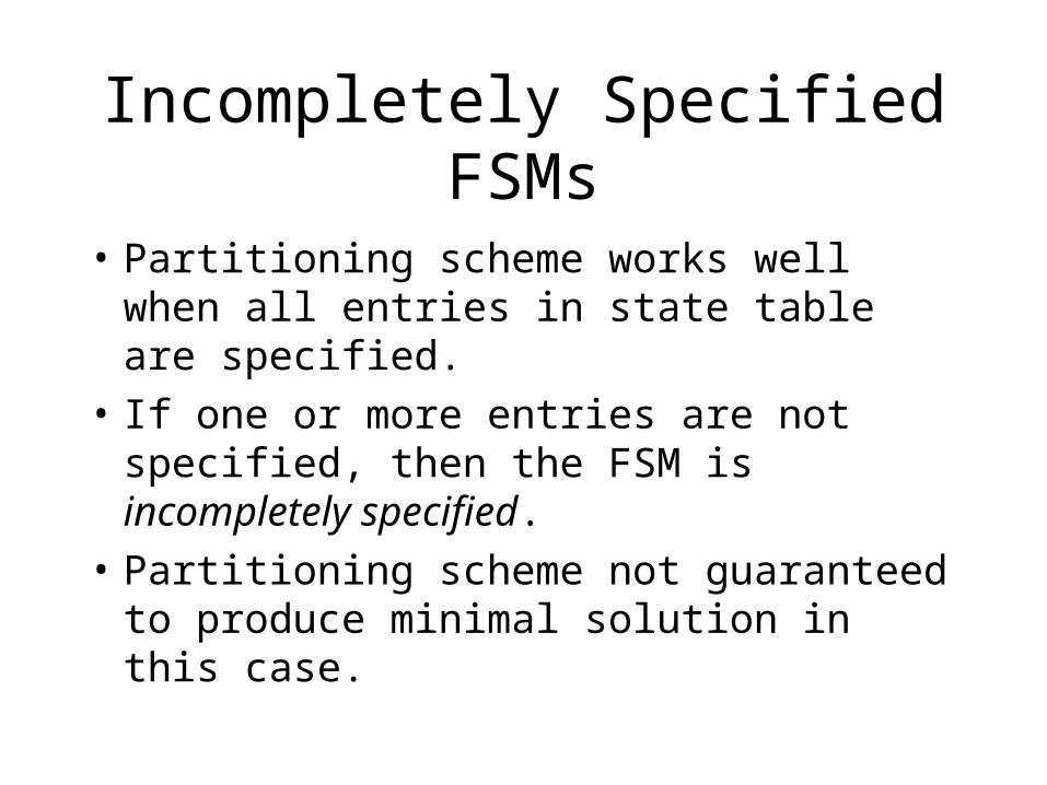
Incompletely Specified FSMs
• Partitioning scheme works well when all entries in state table are specified.
• If one or more entries are not specified, then the FSM is incompletely specified.
• Partitioning scheme not guaranteed to produce minimal solution in this case.

Figure 8.59 Incompletely specified state table for Example 8.7
Present Next state Output z
state w = 0 w = 1 w = 0 w = 1
A B C 0 0 B D 0 C F E 0 1 D B G 0 0 E F C 0 1 F E D 0 1 G F 0
–
–
–
–
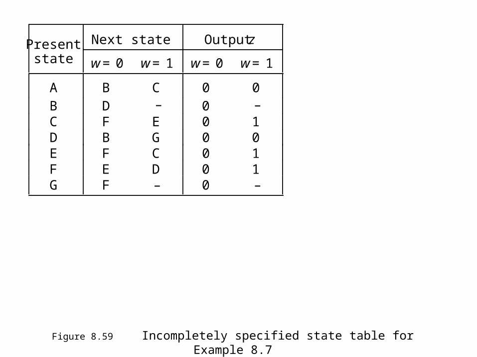
Figure 8.59 Incompletely specified state table for Example 8.7
Present Next state Output z
state w = 0 w = 1 w = 0 w = 1
A B C 0 0 B D 0 C F E 0 1 D B G 0 0 E F C 0 1 F E D 0 1 G F 0
–
–
–
–
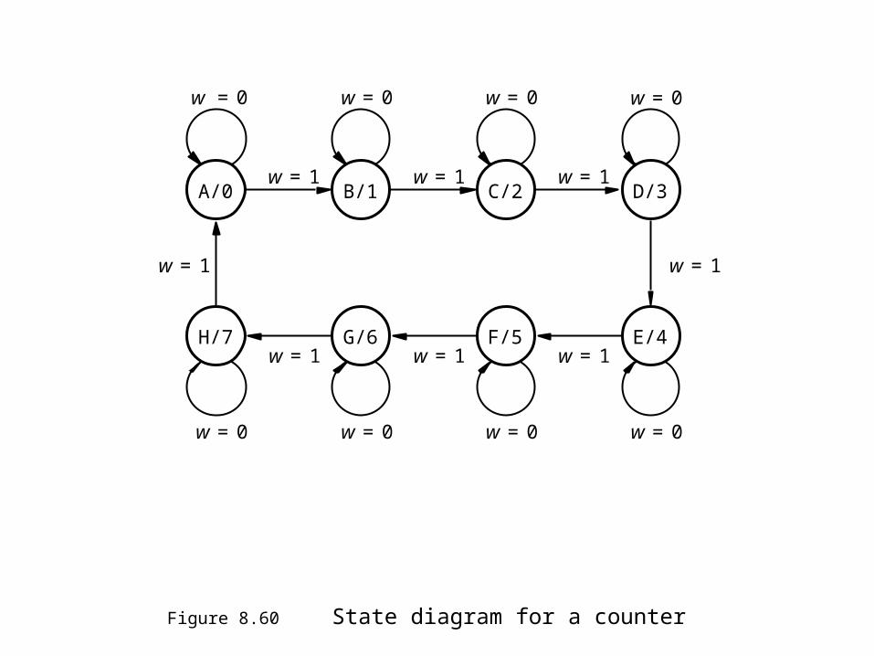
Figure 8.60 State diagram for a counter
w 0=
w 1=
w 0=
w 1=
w 0=
w 1=
w 0=
w 1=
w 0=
w 1=
w 0=
w 1=
w 0=
w 1=
w 0=
w 1=
A/0 B/1 C/2 D/3
E/4F/5G/6H/7

Figure 8.61 State table for the counter
Present Next state Output
state w = 0 w = 1
A A B 0 B B C 1 C C D 2 D D E 3 E E F 4 F F G 5 G G H 6 H H A 7

Figure 8.62 State-assigned table for the counter
Present Next state
state w = 0 w = 1 Count
y 2 y 1 y 0 Y 2 Y 1 Y 0 Y 2 Y 1 Y 0
z 2 z 1 z 0
A 000 000 001 000 B 001 001 010 001 C 010 010 011 010 D 011 011 100 011 E 100 100 101 100 F 101 101 110 101 G 110 110 111 110 H 111 111 000 111

Figure 8.63 Karnaugh maps for D flip-flops for the counter
00 01 11 10
00
01
1
0 1
1
1
0
0
0
0
1 0
0
0
1
1
1 11
10
y 1 y 0 wy2 00 01 11 10
00
01
0
0 0
1
1
1
1
0
1
0 1
0
0
1
1
0 11
10
y 1 y 0 wy2
00 01 11 10
00
01
0
1 1
0
1
0
1
0
1
0 0
0
1
1
0
1 11
10
y 1 y 0 wy2
Y 2 wy2 y 0 y 2 y 1 y 2 w + + + y 0 y 1 y 2 =
Y 0 wy0 wy0 + = Y 1 wy1 y 1 y 0 wy0 y 1 + + =
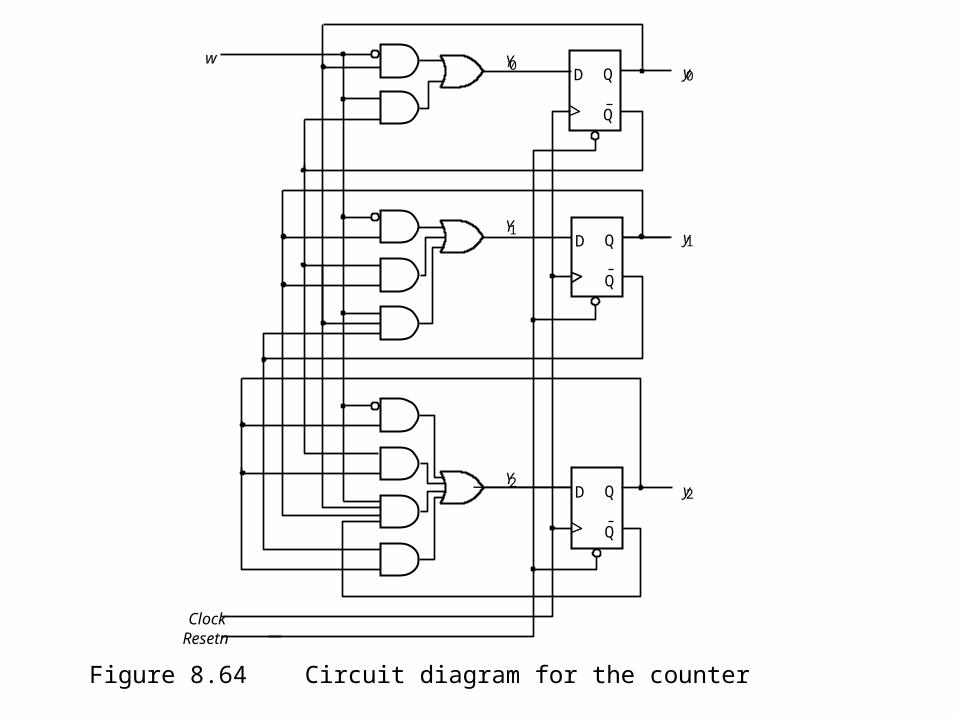
Figure 8.64 Circuit diagram for the counter
D Q
Q
D Q
Q
Clock
y 0 w
y 1
y 2
Y 0
Y 1
Y 2
Resetn
D Q
Q

Implementation Using JK-FF
• If FF in state 0 to remain 0, J=0 and K=d.
• If FF in state 0 to change to 1, J=1 and K=d.
• If FF in state 1 to remain 1, J=d and K=0.
• If FF in state 1 to change to 0, J=d and K=1.
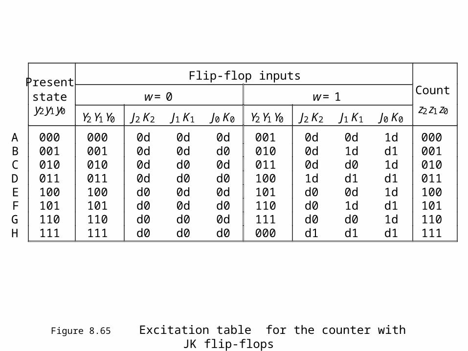
Figure 8.65 Excitation table for the counter with JK flip-flops
Present Flip-flop inputs
state w = 0 w = 1 Count
y 2 y 1 y 0 Y 2 Y 1 Y 0 J 2 K 2 J 1 K 1 J 0 K 0 Y 2 Y 1 Y 0 J 2 K 2 J 1 K 1 J 0 K 0
z 2 z 1 z 0
A 000 000 0d 0d 0d 001 0d 0d 1d 000 B 001 001 0d 0d d0 010 0d 1d d1 001 C 010 010 0d d0 0d 011 0d d0 1d 010 D 011 011 0d d0 d0 100 1d d1 d1 011 E 100 100 d0 0d 0d 101 d0 0d 1d 100 F 101 101 d0 0d d0 110 d0 1d d1 101 G 110 110 d0 d0 0d 111 d0 d0 1d 110 H 111 111 d0 d0 d0 000 d1 d1 d1 111
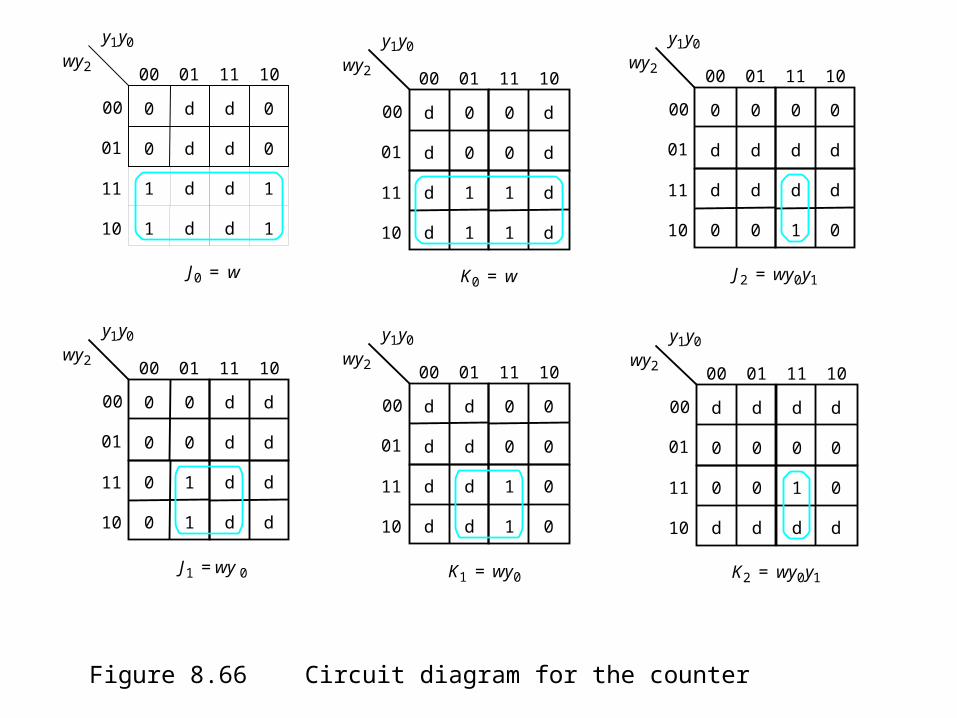
Figure 8.66 Circuit diagram for the counter
00 01 11 10
00
01
0
0 0
d
d
d
d
0
1
0 1
d
d
d
d
011
10
y1y0
wy2
J1 wy0=
00 01 11 10
00
01
d
0 d
d
d
0
0
0
d
1 d
d
d
1
1
111
10
y1y0
wy2
J0 w=
00 01 11 10
00
01
0
d 0
0
0
d
d
d
1
d 1
1
1
d
d
d11
10
y1y0
wy2
00 01 11 10
00
01
d
d d
0
0
0
0
d
d
d d
1
1
0
0
d11
10
y1y0
wy2
K1 wy0=
K0 w=
00 01 11 10
00
01
0
d d
0
d
0
d
0
d
0 0
d
1
d
0
d11
10
y1y0
wy2
J2 wy0y1=
00 01 11 10
00
01
d
0 0
d
0
d
0
d
0
d d
1
d
0
d
011
10
y1y0
wy2
K2 wy0y1=

Figure 8.67 Circuit diagram using JK flip-flops
Clock
Resetn
w J Q
Q K
y 0
y 1
y 2
J Q
Q K
J Q
Q K

Figure 8.68 Factored-form implementation of the counter
Clock
Resetn
w y 0
y 1
y 2
J Q
Q K
J Q
Q K
J Q
Q K
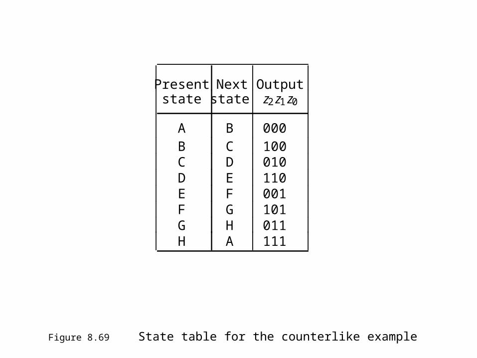
Figure 8.69 State table for the counterlike example
Present Next Outputstate state z 2 z 1 z 0
A B 000 B C 100 C D 010 D E 110 E F 001 F G 101 G H 011 H A 111
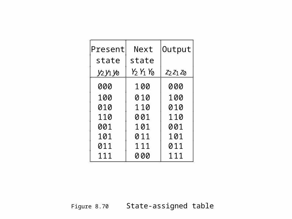
Figure 8.70 State-assigned table
Present Next Outputstate state
y 2 y 1 y 0 Y 2 Y 1 Y 0 z 2 z 1 z 0
000 1 00 0 00100 0 10 1 00010 1 10 0 10110 0 01 1 10001 1 01 0 01101 0 11 1 01011 1 11 0 11111 0 00 1 11

Figure 8.71 Circuit for the counterlike example
D Q
Q
z 0
D Q
Q
D Q
Q
z 1
z 2
w

Figure 8.72 State diagram for the arbiter
Idle
000
1xx
Reset
gnt1 g 1 1 =
x1x
gnt2 g 2 1 =
xx1
gnt3 g 3 1 =
0xx 1xx
01x x0x
001 xx0

Figure 8.73 Alternative style of state diagram for the arbiter
r 1 r 2
r 1 r 2 r 3
Idle
Reset
gnt1 g 1 1 =
gnt2 g 2 1 =
gnt3 g 3 1 =
r 1 r 1
r 1
r 2
r 3
r 2
r 3
r 1 r 2 r 3
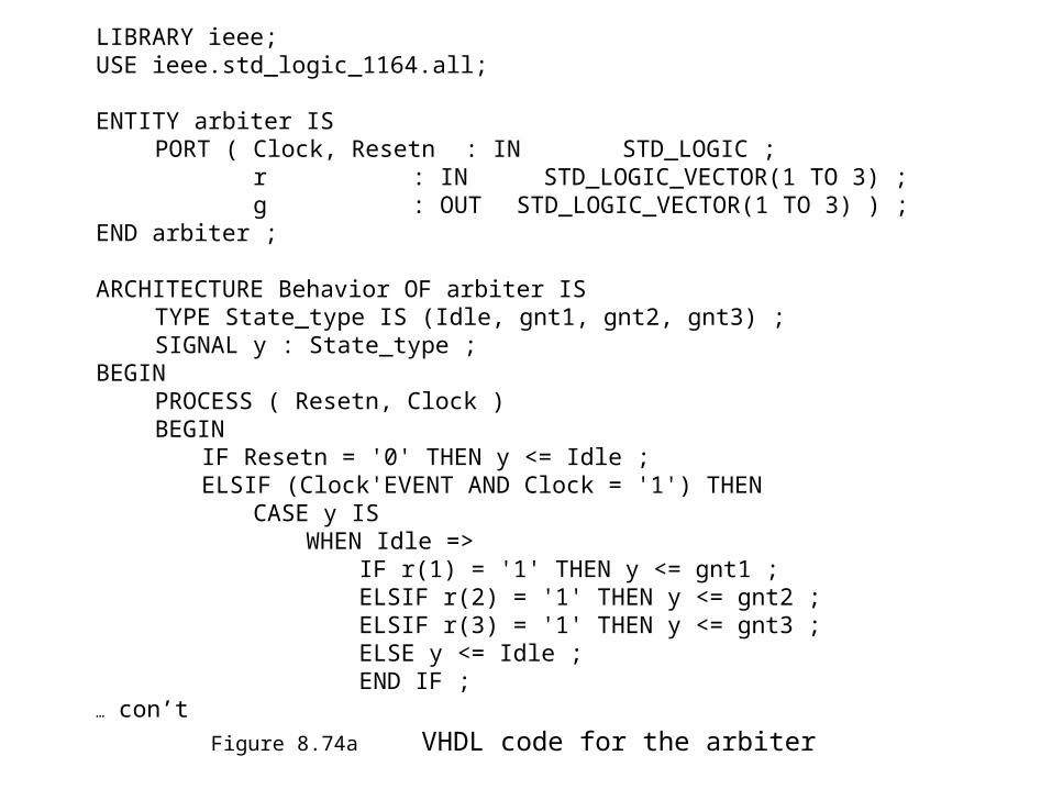
Figure 8.74a VHDL code for the arbiter
LIBRARY ieee;USE ieee.std_logic_1164.all;
ENTITY arbiter ISPORT ( Clock, Resetn : IN STD_LOGIC ;
r : IN STD_LOGIC_VECTOR(1 TO 3) ;g : OUT STD_LOGIC_VECTOR(1 TO 3) ) ;
END arbiter ;
ARCHITECTURE Behavior OF arbiter ISTYPE State_type IS (Idle, gnt1, gnt2, gnt3) ;SIGNAL y : State_type ;
BEGINPROCESS ( Resetn, Clock )BEGIN
IF Resetn = '0' THEN y <= Idle ;ELSIF (Clock'EVENT AND Clock = '1') THEN
CASE y ISWHEN Idle =>
IF r(1) = '1' THEN y <= gnt1 ;ELSIF r(2) = '1' THEN y <= gnt2 ;ELSIF r(3) = '1' THEN y <= gnt3 ;ELSE y <= Idle ;END IF ;
… con’t

Figure 8.74b VHDL code for the arbiter (con’t)
WHEN gnt1 =>IF r(1) = '1' THEN y <= gnt1 ;ELSE y <= Idle ;END IF ;
WHEN gnt2 =>IF r(2) = '1' THEN y <= gnt2 ;ELSE y <= Idle ;END IF ;
WHEN gnt3 =>IF r(3) = '1' THEN y <= gnt3 ;ELSE y <= Idle ;END IF ;
END CASE ;END IF ;
END PROCESS ;g(1) <= '1' WHEN y = gnt1 ELSE '0' ;g(2) <= '1' WHEN y = gnt2 ELSE '0' ;g(3) <= '1' WHEN y = gnt3 ELSE '0' ;
END Behavior ;

Figure 8.75 Incorrect VHDL code for the grant signals
.
.
.PROCESS( y )BEGIN
IF y = gnt1 THEN g(1) <= '1' ;ELSIF y = gnt2 THEN g(2) <= '1' ;ELSIF y = gnt3 THEN g(3) <= '1' ;END IF ;
END PROCESS ;END Behavior ;

Figure 8.76 Correct VHDL code for the grant signals
.
.
.PROCESS( y )BEGIN
g(1) <= '0' ;g(2) <= '0' ;g(3) <= '0' ;IF y = gnt1 THEN g(1) <= '1' ;ELSIF y = gnt2 THEN g(2) <= '1' ;ELSIF y = gnt3 THEN g(3) <= '1' ;END IF ;
END PROCESS ;END Behavior ;
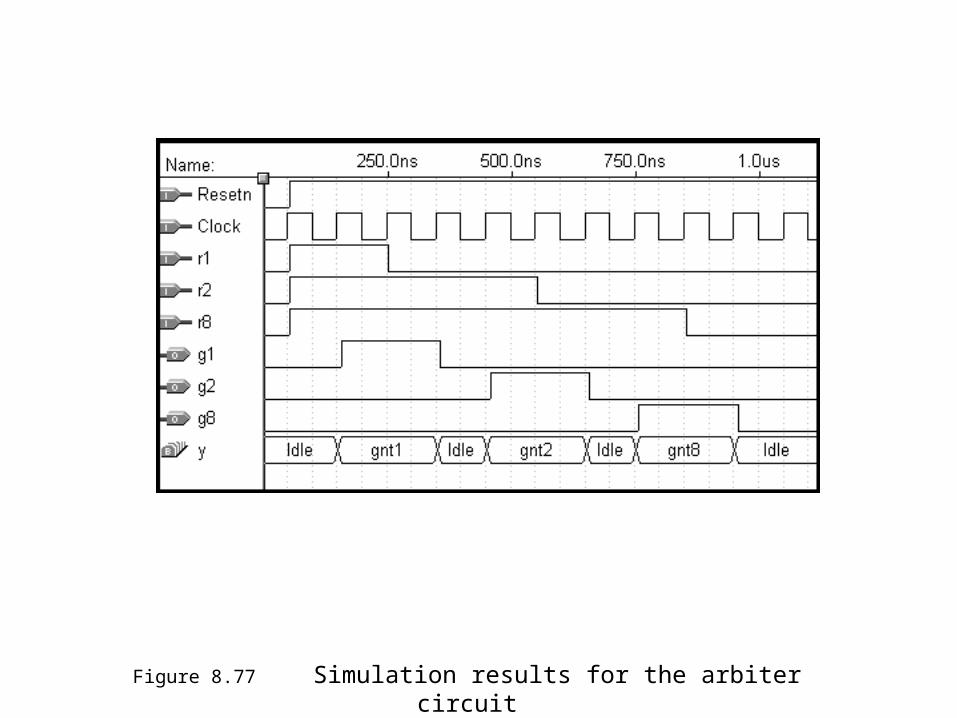
Figure 8.77 Simulation results for the arbiter circuit
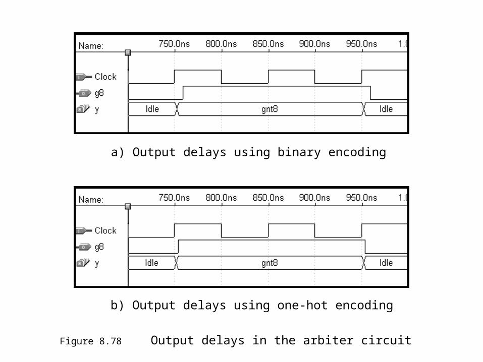
Figure 8.78 Output delays in the arbiter circuit
a) Output delays using binary encoding
b) Output delays using one-hot encoding

Figure 8.80 Circuit for Example 8.8
D Q
Q
D Q
Q
Clock
Resetn
y 2
y 1
Y 2
Y 1
w
z

Figure 8.81 Tables for the circuit in Example 8.8
Present Next State
state w = 0 w = 1 Output
y 2 y 1 Y 2 Y 1 Y 2 Y 1 z
0 0 0 0 01 0 0 1 0 0 10 0 1 0 0 0 11 0 1 1 0 0 11 1
(a)State-assigned table
Present Next state Outputstate w = 0 w = 1 z
A A B 0 B A C 0 C A D 0 D A D 1
(b)State table

Figure 8.82 Circuit for Example 8.9
J Q
Q
Clock
Resetn
y2
y1
J2
J1w
z
K
J Q
QKK2
K1

Figure 8.83 Excitation table
Present Flip-flop inputs
state w = 0 w = 1 Output
y 2 y 1 J 2 K 2 J 1 K 1 J 2 K 2 J 1 K 1 z
00 01 0 1 0 0 1 1 0 01 01 0 1 1 0 1 1 0 10 01 0 1 0 0 1 0 0 11 01 0 1 1 0 1 0 1
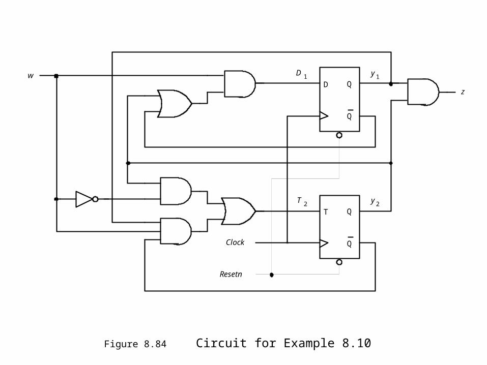
Figure 8.84 Circuit for Example 8.10
Clock
Resetn
y 2
y 1 w
z
T 2
D 1 D Q
Q
T Q
Q

Figure 8.85 Excitation table
Present Flip-flop inputs
state w = 0 w = 1 Output
y 2 y 1 T 2 D 1 T 2 D 1 z
0 0 0 0 01 0 0 1 0 0 10 0 1 0 1 0 01 0 1 1 1 0 01 1

Figure 8.86 Elements used in ASM charts
Output signalsor actions
(Moore type)
State name
Condition expression
0 (False) 1 (True)
Conditional outputs or actions (Mealy type)
(a) State box (b) Decision box
(c) Conditional output box
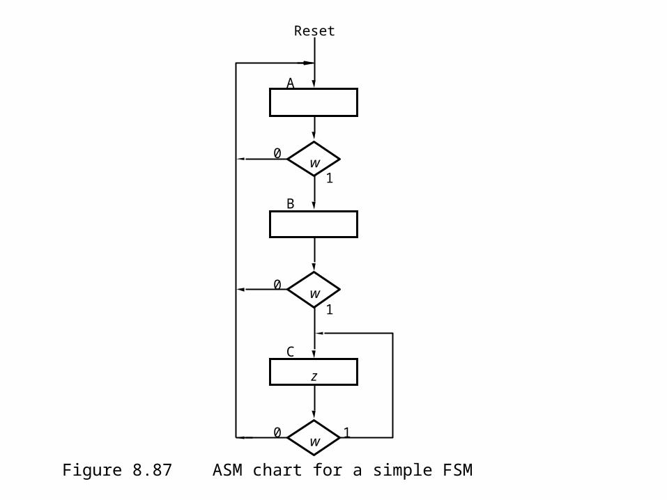
Figure 8.87 ASM chart for a simple FSM
w
w
w 0 1
0
1
0
1
A
B
C
z
Reset

Figure 8.88 ASM chart for the FSM in Figure 8.23
w
w 0 1
0
1
A
B
Reset
z

Figure 8.89 ASM chart for the arbiter
r 1
r 3 0 1
1
Idle
Reset
r 2
r 1
r 3
r 2
gnt1
gnt2
gnt3
1
1
1
0
0
0
g 1
g 2
g 3
0
0
1

Figure 8.90 The general model for a sequential circuit
Combinational circuit
Y k
Y 1
y k
y 1
w 1
w n
z 1
z m
Outputs
Next-statevariables
Present-state variables
Inputs

Formal Model for FSMs
• M = (W, Z, S, , )– W is finite, nonempty set of inputs.– Z is finite, nonempty set of outputs.– S is finite, nonempty set of states. is the state transition function:
• S(t+1) = [W(t),S(t)] is the output function:
(t) = [S(t)] (Moore model)(t) = [W(t),S(t)] (Mealy model)
Summary
• FSM Design (Moore and Mealy)– State minimization– State assignment– Using CAD tools and VHDL