CSE241 VLSI Digital Circuits Winter 2003 Lecture 18:...
35
CSE241A L18 Cost.1 Kahng, UCSD ©2003 CSE241 VLSI Digital Circuits Winter 2003 Lecture 18: Cost
Transcript of CSE241 VLSI Digital Circuits Winter 2003 Lecture 18:...
CSE241A L18 Cost.1 Kahng, UCSD ©2003
CSE241VLSI Digital Circuits
Winter 2003
Lecture 18: Cost
CSE241A L18 Cost.2 Kahng, UCSD ©2003
LogisticsPlan for next four meetings:
Today: Cost (+Project discussion)Next Tuesday: IO, Memories and IPNext Thursday: Future of VLSI (+Project discussion)
Project schedule
Readingshttp://www.dac.com/38th/acceptedpapers.nsf/9cfb1ebaaf59043587256a6a00031f78/5383bbf67973bfc488256a78006d4b42/$FILE/2_2.PDF (W. Maly invited paper, Session 2, DAC-2001 – “IC Design in High-Cost Nanometer-Technologies Era”http://www.nassda.com/ROIWhitePaper.pdf (Nassda Corporation, “Maximizing Silicon ROI: The Cost of Failure and Success”)See also Wright, Williams and Kelly website (SEMATECH Cost of Ownership Model)
CSE241A L18 Cost.3 Kahng, UCSD ©2003
Overview of Cost
Source: Nassda Corporation
CSE241A L18 Cost.4 Kahng, UCSD ©2003
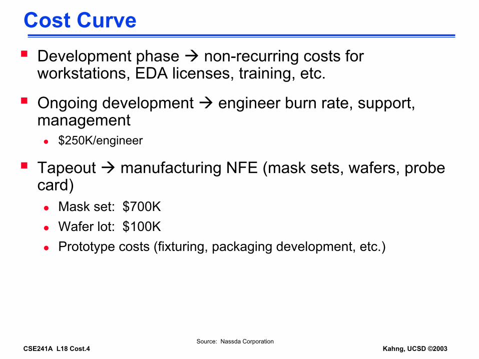
Cost CurveDevelopment phase non-recurring costs for workstations, EDA licenses, training, etc.
Ongoing development engineer burn rate, support, management
$250K/engineer
Tapeout manufacturing NFE (mask sets, wafers, probe card)
Mask set: $700KWafer lot: $100KPrototype costs (fixturing, packaging development, etc.)
Source: Nassda Corporation
CSE241A L18 Cost.5 Kahng, UCSD ©2003
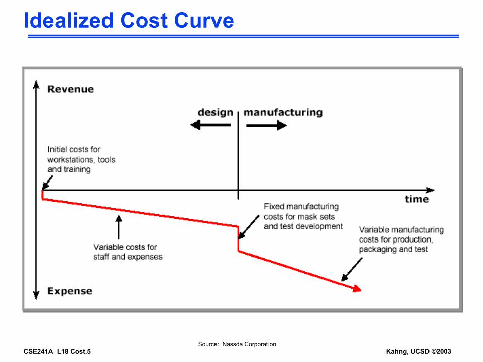
Idealized Cost Curve
Source: Nassda Corporation
CSE241A L18 Cost.6 Kahng, UCSD ©2003
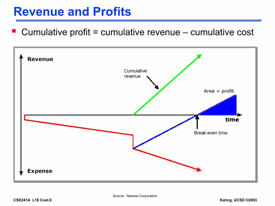
Revenue and ProfitsCumulative profit = cumulative revenue – cumulative cost
Source: Nassda Corporation
CSE241A L18 Cost.7 Kahng, UCSD ©2003
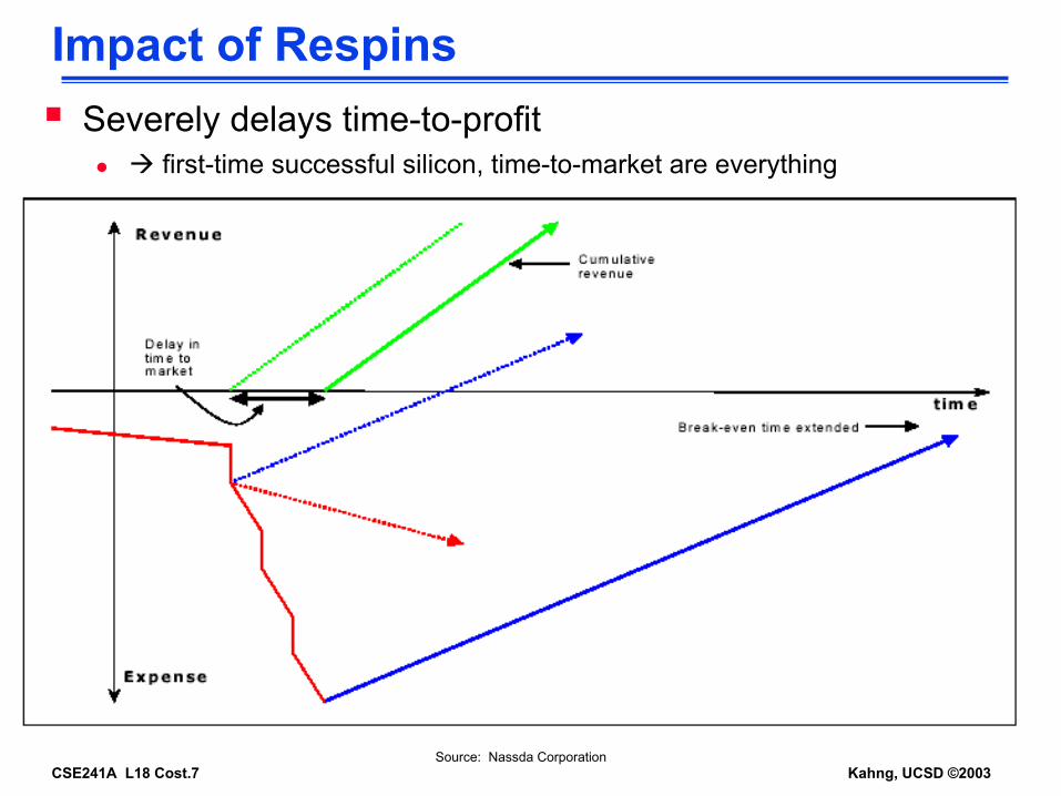
Impact of RespinsSeverely delays time-to-profit
first-time successful silicon, time-to-market are everything
Source: Nassda Corporation
CSE241A L18 Cost.8 Kahng, UCSD ©2003
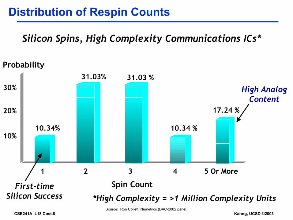
Distribution of Respin Counts
10.34%
31.03% 31.03 %
10.34 %
17.24 %
1 2 3 4 5 Or More
Silicon Spins, High Complexity Communications ICs*
Probability
Spin Count
High AnalogContent
10%
20%
30%
First-timeSilicon Success *High Complexity = >1 Million Complexity Units
Source: Ron Collett, Numetrics (DAC-2002 panel)

CSE241A L18 Cost.9 Kahng, UCSD ©2003
Shrinking Product Life CycleNarrower opportunity for profit
Source: Nassda Corporation
CSE241A L18 Cost.10 Kahng, UCSD ©2003
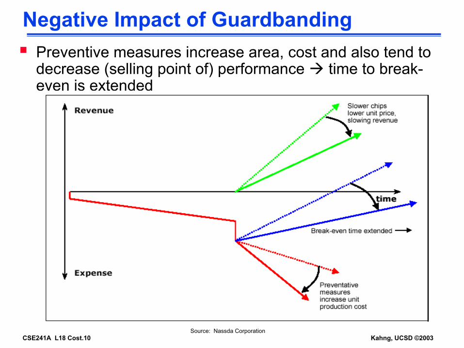
Negative Impact of GuardbandingPreventive measures increase area, cost and also tend to decrease (selling point of) performance time to break-even is extended
Source: Nassda Corporation
CSE241A L18 Cost.11 Kahng, UCSD ©2003
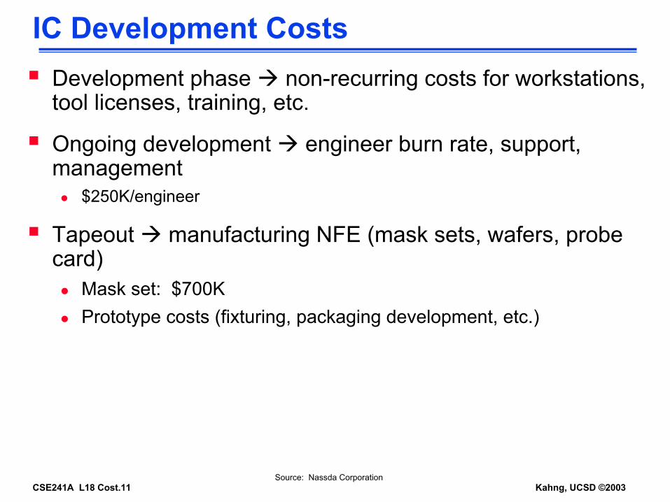
IC Development CostsDevelopment phase non-recurring costs for workstations, tool licenses, training, etc.
Ongoing development engineer burn rate, support, management
$250K/engineer
Tapeout manufacturing NFE (mask sets, wafers, probe card)
Mask set: $700KPrototype costs (fixturing, packaging development, etc.)
Source: Nassda Corporation
CSE241A L18 Cost.12 Kahng, UCSD ©2003
System Costs
Source: Nassda Corporation
CSE241A L18 Cost.13 Kahng, UCSD ©2003
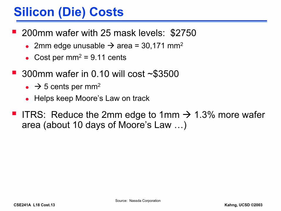
Silicon (Die) Costs200mm wafer with 25 mask levels: $2750
2mm edge unusable area = 30,171 mm2
Cost per mm2 = 9.11 cents
300mm wafer in 0.10 will cost ~$3500 5 cents per mm2
Helps keep Moore’s Law on track
ITRS: Reduce the 2mm edge to 1mm 1.3% more wafer area (about 10 days of Moore’s Law …)
Source: Nassda Corporation
CSE241A L18 Cost.14 Kahng, UCSD ©2003
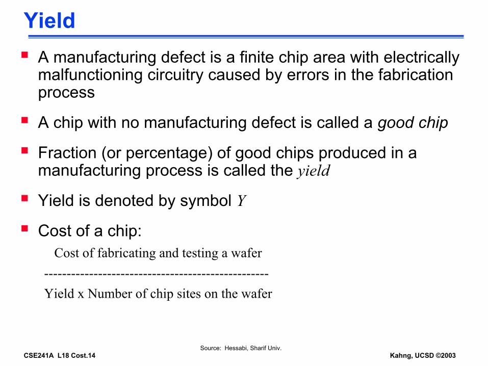
YieldA manufacturing defect is a finite chip area with electrically malfunctioning circuitry caused by errors in the fabrication process
A chip with no manufacturing defect is called a good chip
Fraction (or percentage) of good chips produced in a manufacturing process is called the yield
Yield is denoted by symbol Y
Cost of a chip:Cost of fabricating and testing a wafer
--------------------------------------------------Yield x Number of chip sites on the wafer
Source: Hessabi, Sharif Univ.
CSE241A L18 Cost.15 Kahng, UCSD ©2003
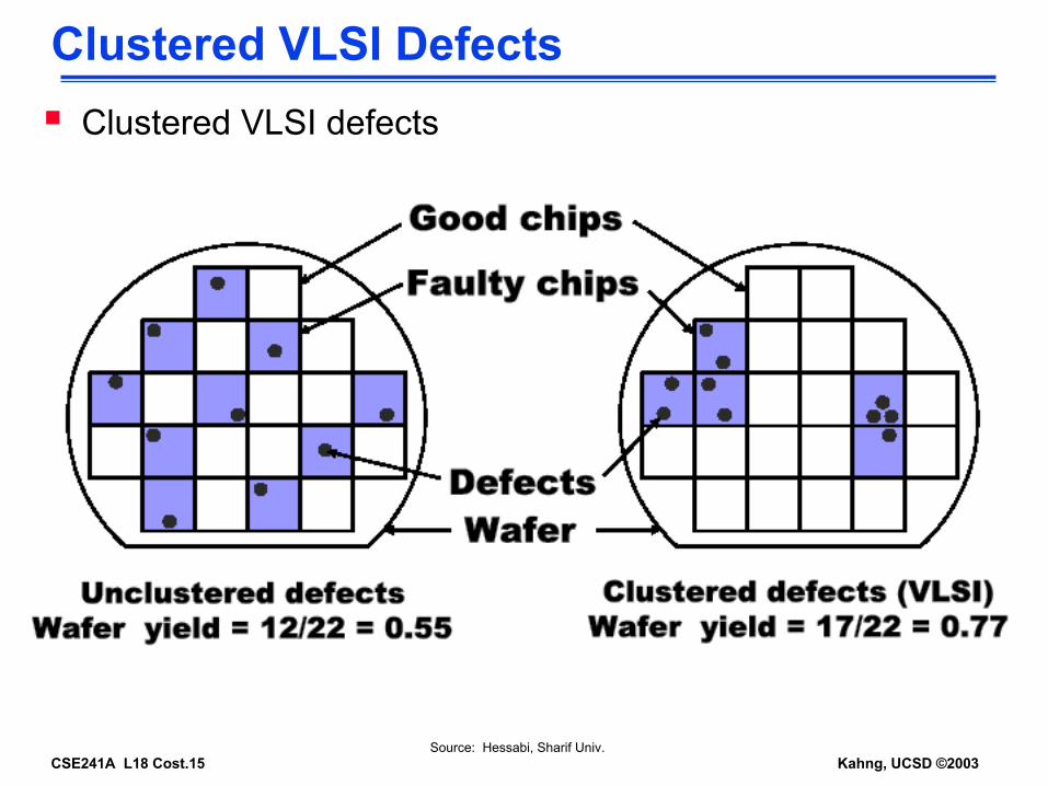
Clustered VLSI DefectsClustered VLSI defects
Source: Hessabi, Sharif Univ.
CSE241A L18 Cost.16 Kahng, UCSD ©2003
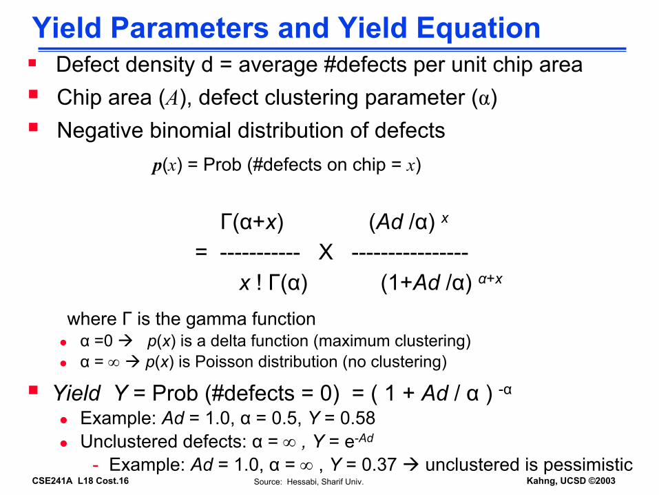
Yield Parameters and Yield EquationDefect density d = average #defects per unit chip areaChip area (A), defect clustering parameter (α)Negative binomial distribution of defects
p(x) = Prob (#defects on chip = x)
Γ(α+x) (Ad /α) x
= ----------- X ----------------x ! Γ(α) (1+Ad /α) α+x
where Γ is the gamma functionα =0 p(x) is a delta function (maximum clustering)α = ∞ p(x) is Poisson distribution (no clustering)
Yield Y = Prob (#defects = 0) = ( 1 + Ad / α ) -αExample: Ad = 1.0, α = 0.5, Y = 0.58Unclustered defects: α = ∞ , Y = e-Ad
- Example: Ad = 1.0, α = ∞ , Y = 0.37 unclustered is pessimisticSource: Hessabi, Sharif Univ.
CSE241A L18 Cost.17 Kahng, UCSD ©2003
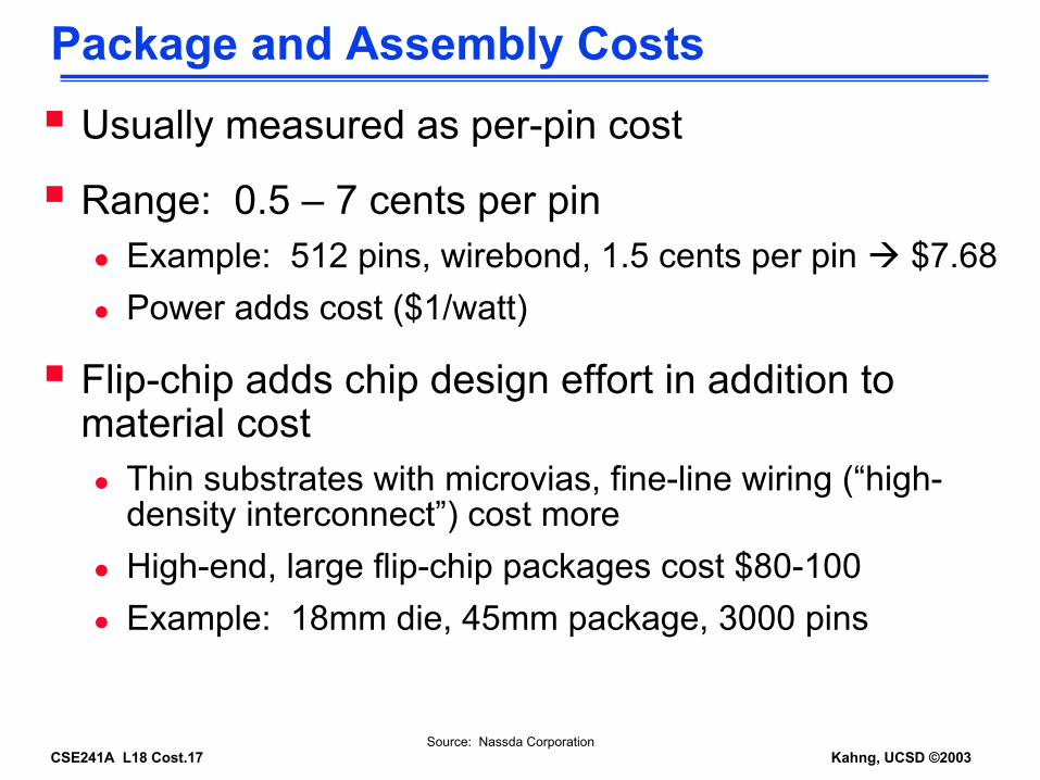
Package and Assembly CostsUsually measured as per-pin cost
Range: 0.5 – 7 cents per pinExample: 512 pins, wirebond, 1.5 cents per pin $7.68Power adds cost ($1/watt)
Flip-chip adds chip design effort in addition to material cost
Thin substrates with microvias, fine-line wiring (“high-density interconnect”) cost moreHigh-end, large flip-chip packages cost $80-100Example: 18mm die, 45mm package, 3000 pins
Source: Nassda Corporation
CSE241A L18 Cost.18 Kahng, UCSD ©2003
Design for TestDFT on chip impacts board, system level economics
Costs- Reduced yield due to area- Overhead, yield loss due to non-functional tests
Benefits- Reduced ATE cost due to self-test- Less expensive alternatives to burn-in
Source: Hessabi, Sharif Univ.
CSE241A L18 Cost.19 Kahng, UCSD ©2003
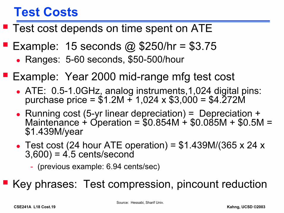
Test CostsTest cost depends on time spent on ATEExample: 15 seconds @ $250/hr = $3.75
Ranges: 5-60 seconds, $50-500/hour
Example: Year 2000 mid-range mfg test costATE: 0.5-1.0GHz, analog instruments,1,024 digital pins: purchase price = $1.2M + 1,024 x $3,000 = $4.272MRunning cost (5-yr linear depreciation) = Depreciation + Maintenance + Operation = $0.854M + $0.085M + $0.5M = $1.439M/yearTest cost (24 hour ATE operation) = $1.439M/(365 x 24 x 3,600) = 4.5 cents/second
- (previous example: 6.94 cents/sec)
Key phrases: Test compression, pincount reductionSource: Hessabi, Sharif Univ.
CSE241A L18 Cost.20 Kahng, UCSD ©2003
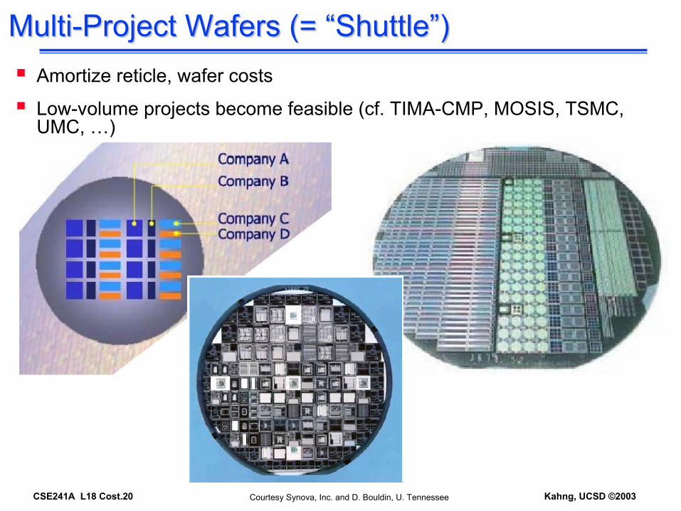
MultiMulti--Project Wafers (= “Shuttle”)Project Wafers (= “Shuttle”)Amortize reticle, wafer costs
Low-volume projects become feasible (cf. TIMA-CMP, MOSIS, TSMC, UMC, …)
Courtesy Synova, Inc. and D. Bouldin, U. Tennessee
CSE241A L18 Cost.21 Kahng, UCSD ©2003
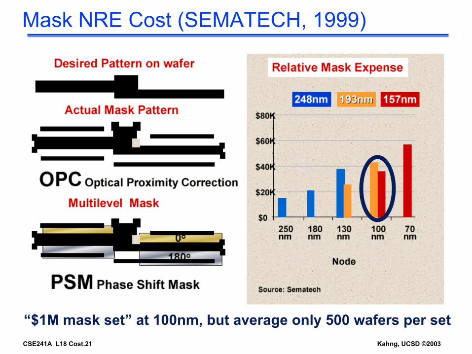
Mask NRE Cost (SEMATECH, 1999)
“$1M mask set” at 100nm, but average only 500 wafers per set
CSE241A L18 Cost.22 Kahng, UCSD ©2003
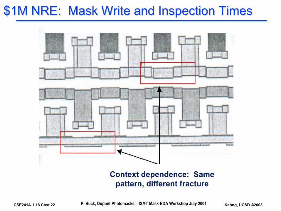
Context dependence: Same pattern, different fracture
P. Buck, Dupont Photomasks – ISMT Mask-EDA Workshop July 2001
$1M NRE: Mask Write and Inspection Times$1M NRE: Mask Write and Inspection Times
CSE241A L18 Cost.23 Kahng, UCSD ©2003
How to Save Total NRE + Wafer Cost?Multi-project wafers
Not just packing dependentDepends on similar densities, speeds, etc. (process biases)Depends on volumes
Metal-only respinsSpare (“bonus”) resources in synthesis, layout
How to allocate? How to locate?
Source: Hessabi, Sharif Univ.
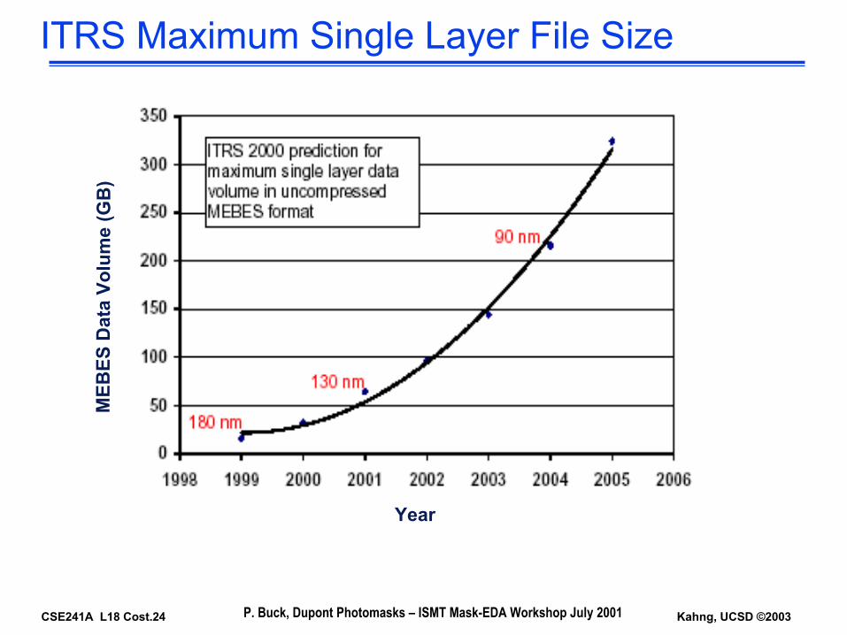
CSE241A L18 Cost.24 Kahng, UCSD ©2003
MEB
ES D
a ta
Volu
me
( GB
)
Year
P. Buck, Dupont Photomasks – ISMT Mask-EDA Workshop July 2001
ITRS Maximum Single Layer File Size
CSE241A L18 Cost.25 Kahng, UCSD ©2003
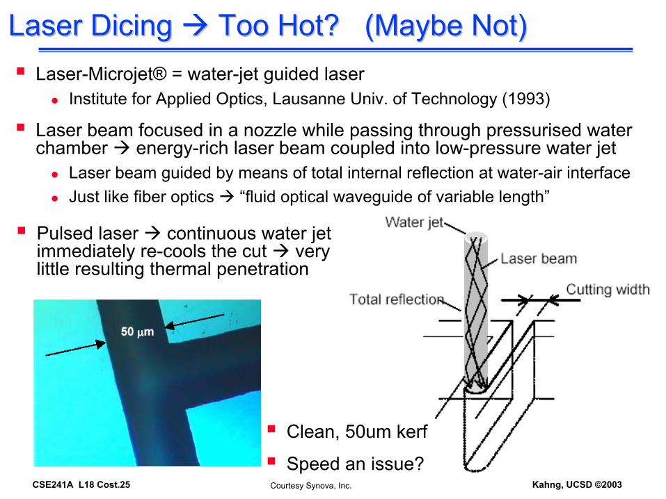
Laser Dicing Laser Dicing Too Hot? (Maybe Not)Too Hot? (Maybe Not)Laser-Microjet® = water-jet guided laser
Institute for Applied Optics, Lausanne Univ. of Technology (1993)
Laser beam focused in a nozzle while passing through pressurised water chamber energy-rich laser beam coupled into low-pressure water jet
Laser beam guided by means of total internal reflection at water-air interfaceJust like fiber optics “fluid optical waveguide of variable length”
Courtesy Synova, Inc.
Pulsed laser continuous water jet immediately re-cools the cut very little resulting thermal penetration
Clean, 50um kerf
Speed an issue?
CSE241A L18 Cost.26 Kahng, UCSD ©2003
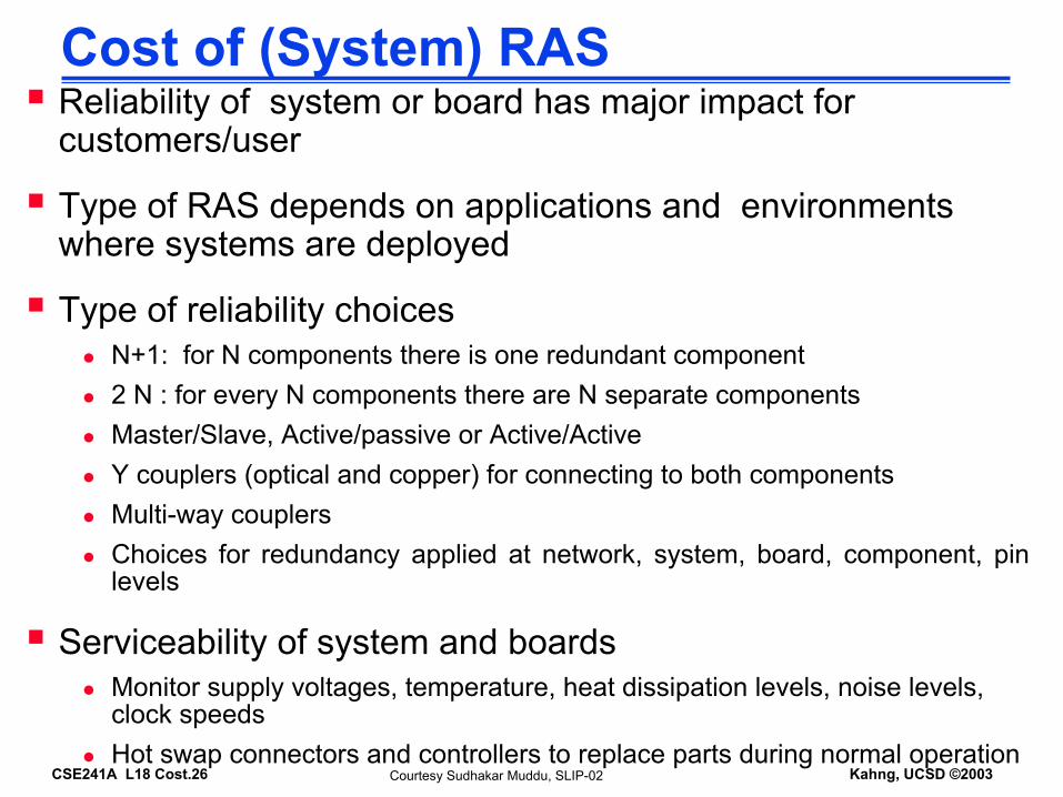
Cost of (System) RASReliability of system or board has major impact for customers/user
Type of RAS depends on applications and environments where systems are deployed
Type of reliability choicesN+1: for N components there is one redundant component 2 N : for every N components there are N separate componentsMaster/Slave, Active/passive or Active/ActiveY couplers (optical and copper) for connecting to both componentsMulti-way couplers Choices for redundancy applied at network, system, board, component, pin levels
Serviceability of system and boards Monitor supply voltages, temperature, heat dissipation levels, noise levels, clock speedsHot swap connectors and controllers to replace parts during normal operation
Courtesy Sudhakar Muddu, SLIP-02
CSE241A L18 Cost.27 Kahng, UCSD ©2003
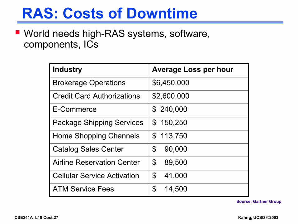
RAS: Costs of DowntimeWorld needs high-RAS systems, software, components, ICs
$ 14,500ATM Service Fees
$ 41,000Cellular Service Activation
$ 89,500Airline Reservation Center
$ 90,000Catalog Sales Center
$ 113,750Home Shopping Channels
$ 150,250Package Shipping Services
$ 240,000E-Commerce
$2,600,000Credit Card Authorizations
$6,450,000Brokerage Operations
Average Loss per hourIndustry
Source: Gartner Group
CSE241A L18 Cost.28 Kahng, UCSD ©2003
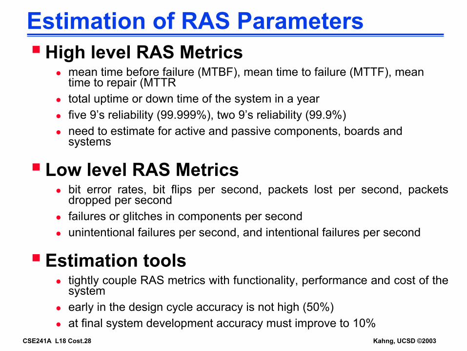
Estimation of RAS ParametersHigh level RAS Metrics
mean time before failure (MTBF), mean time to failure (MTTF), mean time to repair (MTTRtotal uptime or down time of the system in a yearfive 9’s reliability (99.999%), two 9’s reliability (99.9%)need to estimate for active and passive components, boards and systems
Low level RAS Metricsbit error rates, bit flips per second, packets lost per second, packets dropped per secondfailures or glitches in components per secondunintentional failures per second, and intentional failures per second
Estimation tools tightly couple RAS metrics with functionality, performance and cost of the systemearly in the design cycle accuracy is not high (50%)at final system development accuracy must improve to 10%
CSE241A L18 Cost.29 Kahng, UCSD ©2003
Design Costs
Source: Nassda Corporation
CSE241A L18 Cost.30 Kahng, UCSD ©2003
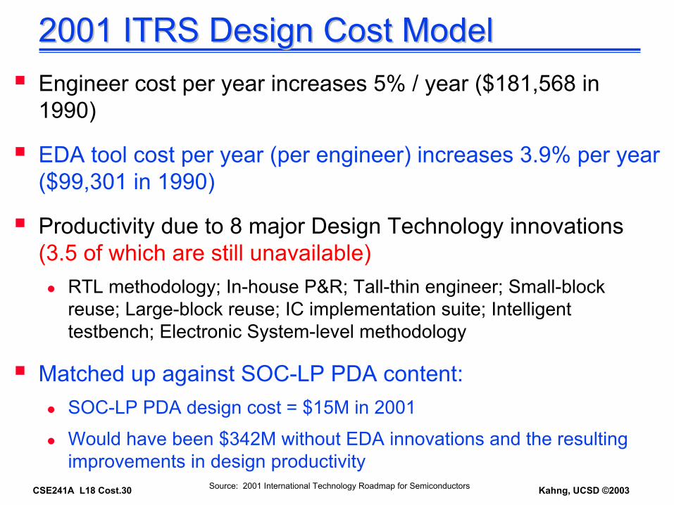
2001 ITRS Design Cost Model2001 ITRS Design Cost ModelEngineer cost per year increases 5% / year ($181,568 in 1990)
EDA tool cost per year (per engineer) increases 3.9% per year ($99,301 in 1990)
Productivity due to 8 major Design Technology innovations (3.5 of which are still unavailable)
RTL methodology; In-house P&R; Tall-thin engineer; Small-block reuse; Large-block reuse; IC implementation suite; Intelligent testbench; Electronic System-level methodology
Matched up against SOC-LP PDA content:SOC-LP PDA design cost = $15M in 2001
Would have been $342M without EDA innovations and the resulting improvements in design productivity
Source: 2001 International Technology Roadmap for Semiconductors
CSE241A L18 Cost.31 Kahng, UCSD ©2003
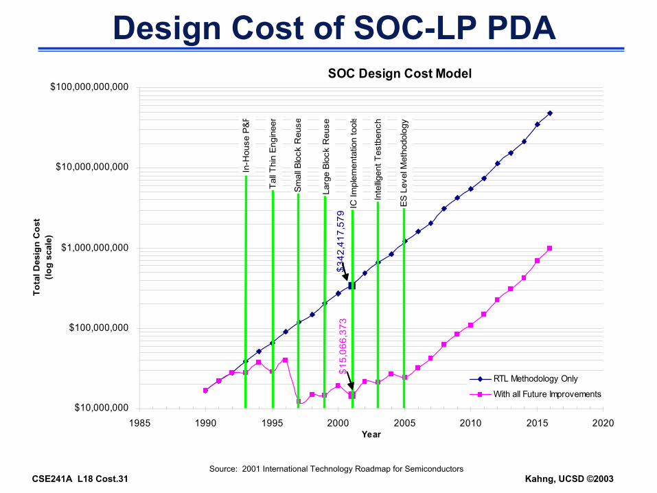
SOC Design Cost Model
$342
,417
,579
$15,
066,
373
$10,000,000
$100,000,000
$1,000,000,000
$10,000,000,000
$100,000,000,000
1985 1990 1995 2000 2005 2010 2015 2020Year
Tota
l Des
ign
Cos
t (lo
g sc
ale)
RTL Methodology Only
With all Future Improvements
In-H
ouse
P&
R
Tall T
hin
Engi
neer
Sm
all B
lock
Reu
se
IC Im
plem
enta
tion
tool
s
Larg
e Bl
ock
Reu
se
Inte
lligen
t Tes
tben
ch
ES L
evel
Met
hodo
logy
Design Cost of SOC-LP PDA
Source: 2001 International Technology Roadmap for Semiconductors

CSE241A L18 Cost.32 Kahng, UCSD ©2003
Why Teams Succeed: Better Planning
Chip Complexity = ƒ(circuit types, timing, reuse, power . . .)
Design Productivity =Effort = ƒ(Eng. & mgmt. skills, EDA tools, spec stability,
mfg. process stability, etc.)
Complexity
Effort
Rate of Effort Consumption = ƒ(best practices)
Quality of Design Process, e.g. spin count probability density function
Key Milestones -- e.g. ƒ(effort consumed, bug rate)
Source: Ron Collett, Numetrics (DAC-2002 panel)
CSE241A L18 Cost.33 Kahng, UCSD ©2003
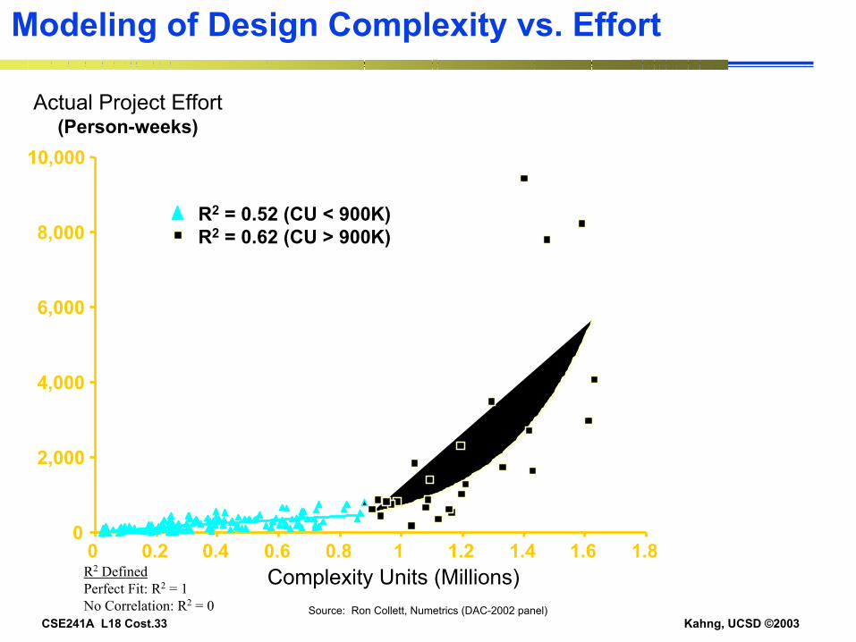
Modeling of Design Complexity vs. Effort
Complexity Units (Millions)
Actual Project Effort(Person-weeks)
R2 DefinedPerfect Fit: R2 = 1No Correlation: R2 = 0
Relationship Between Predicted Project Effort and Actual Project Effort
R2 = 0.52 (CU < 900K)R2 = 0.62 (CU > 900K)
0
2,000
4,000
6,000
8,000
10,000
0 0.2 0.4 0.6 0.8 1 1.2 1.4 1.6 1.8
Source: Ron Collett, Numetrics (DAC-2002 panel)
CSE241A L18 Cost.34 Kahng, UCSD ©2003
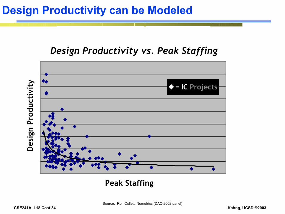
Design Productivity can be Modeled
Design Productivity vs. Peak Staffing
Des
ign
Prod
ucti
vity
Peak Staffing
= IC Projects
Source: Ron Collett, Numetrics (DAC-2002 panel)
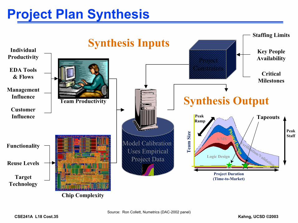
CSE241A L18 Cost.35 Kahng, UCSD ©2003
Model Calibration Uses Empirical
Project Data
Project Plan Synthesis
Synthesis Inputs
Team Productivity
Chip Complexity
IndividualProductivity
EDA Tools& Flows
ManagementInfluence
CustomerInfluence
Functionality
Reuse Levels
TargetTechnology
Staffing Limits
Key PeopleAvailability
CriticalMilestones
ProjectConstraints
Synthesis Output
Tea
m S
ize Peak
Staff
Project Duration(Time-to-Market)
Peak Ramp
Verification/Validation.
Logic Design
Physical Design
A/MS
Tapeouts
Source: Ron Collett, Numetrics (DAC-2002 panel)