8085 Paper Presentation slides,ppt,microprocessor 8085 ,guide, instruction set
Upload
nguyendieuCategory
view
220download
4
1
CS2259 - Microprocessors Lab
IV Semester IT
Syllabus
1. Programming with 8085
2. Programming with 8086-experiments including BIOS/DOS calls:
Keyboard control
Display
File Manipulation
3. Interfacing with 8085/8086-8255,8253 4. Interfacing with 8085/8086-8279,8251
5. 8051 Microcontroller based experiments for Control
Applications 6. Mini- Project

2
1. INTRODUCTION TO 8085
INTEL 8085 is one of the most popular 8-bit microprocessor capable of
addressing 64 KB of memory and its architecture is simple. The device has 40 pins,
requires +5 V power supply and can operate with 3MHz single phase clock.
ALU (Arithmetic Logic Unit):
The 8085A has a simple 8-bit ALU and it works in coordination with the
accumulator, temporary registers, 5 flags and arithmetic and logic circuits. ALU has
the capability of performing several mathematical and logical operations. The
temporary registers are used to hold the data during an arithmetic and logic operation.
The result is stored in the accumulator and the flags are set or reset according to the
result of the operation. The flags are affected by the arithmetic and logic operation.
They are as follows:
Sign flag
After the execution of the arithmetic - logic operation if the bit D7
of the result is 1, the sign flag is set. This flag is used with signed
numbers. If it is 1, it is a negative number and if it is 0, it is a positive
number.
Zero flag
The zero flag is set if the ALU operation results in zero. This flag
is modified by the result in the accumulator as well as in other registers.
Auxillary carry flag
In an arithmetic operation when a carry is generated by digit D3
and passed on to D4, the auxillary flag is set.
Parity flag
After arithmetic – logic operation, if the result has an even number
of 1’s the flag is set. If it has odd number of 1’s it is reset.
Carry flag
If an arithmetic operation results in a carry, the carry flag is set.
The carry flag also serves as a borrow flag for subtraction.

3
Timing and control unit
This unit synchronizes all the microprocessor operation with a clock and
generates the control signals necessary for communication between the
microprocessor and peripherals. The control signals RD (read) and WR (write)
indicate the availability of data on the data bus.
Instruction register and decoder
The instruction register and decoder are part of the ALU. When an instruction is
fetched from memory it is loaded in the instruction register. The decoder decodes the
instruction and establishes the sequence of events to follow.
Register array
The 8085 has six general purpose registers to store 8-bit data during program
execution. These registers are identified as B, C, D, E, H and L. they can be combined
as BC, DE and HL to perform 16-bit operation.
Accumulator
Accumulator is an 8-bit register that is part of the ALU. This register is used to
store 8-bit data and to perform arithmetic and logic operation. The result of an
operation is stored in the accumulator.
Program counter
The program counter is a 16-bit register used to point to the memory address of
the next instruction to be executed.
Stack pointer
It is a 16-bit register which points to the memory location in R/W memory, called
the Stack.
4
Communication lines
8085 microprocessor performs data transfer operations using three communication
lines called buses. They are address bus, data bus and control bus.
Address bus – it is a group of 16-bit lines generally identified as A0 – A15.
The address bus is unidirectional i.e., the bits flow in one direction from
microprocessor to the peripheral devices. It is capable of addressing 216
memory locations.
Data bus – it is a group of 8 lines used for data flow and it is bidirectional.
The data ranges from 00 – FF.
Control bus – it consist of various single lines that carry synchronizing
signals. The microprocessor uses such signals for timing purpose.
5
2(A). 8 BIT DATA ADDITION
AIM:
To add two 8 bit numbers stored at consecutive memory locations.
ALGORITHM:
1. Initialize memory pointer to data location.
2. Get the first number from memory in accumulator.
3. Get the second number and add it to the accumulator.
4. Store the answer at another memory location.
RESULT:
Thus the 8 bit numbers stored at 4500 &4501 are added and the result stored at 4502 &
4503.

6
FLOW CHART:
NO
YES
START
[HL] 4500H
[A] [M]
[A] [A]+[M]
[HL] [HL]+1
STOP
[HL] [HL]+1
[M] [A]
[C] 00H
[M] [C]
[HL] [HL]+1
Is there a
Carry ?
[C] [C]+1

7
PROGRAM:
ADDRESS OPCODE LABEL MNEMONICS OPERAND COMMENT
4100 START MVI C, 00 Clear C reg.
4101
4102 LXI H, 4500 Initialize HL reg. to
4500 4103
4104
4105 MOV A, M Transfer first data to
accumulator
4106 INX H Increment HL reg. to
point next memory
Location.
4107 ADD M Add first number to
acc. Content.
4108 JNC L1 Jump to location if
result does not yield
carry. 4109
410A
410B INR C Increment C reg.
410C L1 INX H Increment HL reg. to
point next memory
Location.
410D MOV M, A Transfer the result from
acc. to memory.
410E INX H Increment HL reg. to
point next memory
Location.
410F MOV M, C Move carry to memory
4110 HLT Stop the program
OBSERVATION:
INPUT OUTPUT
4500 4502
4501 4503
8
2(B). 8 BIT DATA SUBTRACTION
AIM:
To Subtract two 8 bit numbers stored at consecutive memory locations.
ALGORITHM:
1. Initialize memory pointer to data location.
2. Get the first number from memory in accumulator.
3. Get the second number and subtract from the accumulator.
4. If the result yields a borrow, the content of the acc. is complemented and 01H is
added to it (2’s complement). A register is cleared and the content of that reg. is
incremented in case there is a borrow. If there is no borrow the content of the acc.
is directly taken as the result.
5. Store the answer at next memory location.
RESULT:
Thus the 8 bit numbers stored at 4500 &4501 are subtracted and the result stored at 4502
& 4503.

9
FLOW CHART:
NO
YES
START
[HL] 4500H
[A] [M]
Is there a
Borrow ?
[A] [A]-[M]
[HL] [HL]+1
[C] 00H
[C] [C]+1
STOP
[HL] [HL]+1
[M] [A]
[M] [C]
[HL] [HL]+1
Complement [A]
Add 01H to [A]

10
PROGRAM:
ADDRESS OPCODE LABEL MNEMONICS OPERAND COMMENT
4100 START MVI C, 00 Clear C reg.
4102
4102 LXI H, 4500 Initialize HL reg. to
4500 4103
4104
4105 MOV A, M Transfer first data to
accumulator
4106 INX H Increment HL reg. to
point next mem.
Location.
4107 SUB M Subtract first number
from acc. Content.
4108 JNC L1 Jump to location if
result does not yield
borrow. 4109
410A
410B INR C Increment C reg.
410C CMA Complement the Acc.
content
410D ADI 01H Add 01H to content of
acc. 410E
410F L1 INX H Increment HL reg. to
point next mem.
Location.
4110 MOV M, A Transfer the result from
acc. to memory.
4111 INX H Increment HL reg. to
point next mem.
Location.
4112 MOV M, C Move carry to mem.
4113 HLT Stop the program
OBSERVATION:
INPUT OUTPUT
4500 4502
4501 4503
11
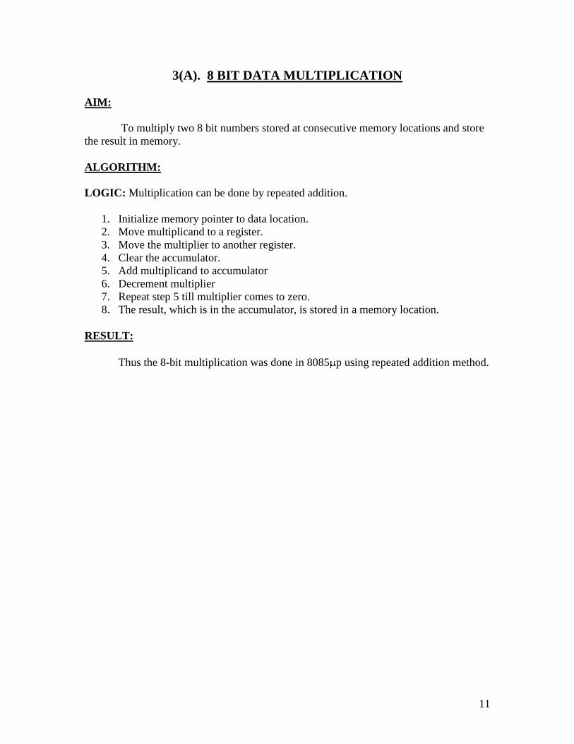
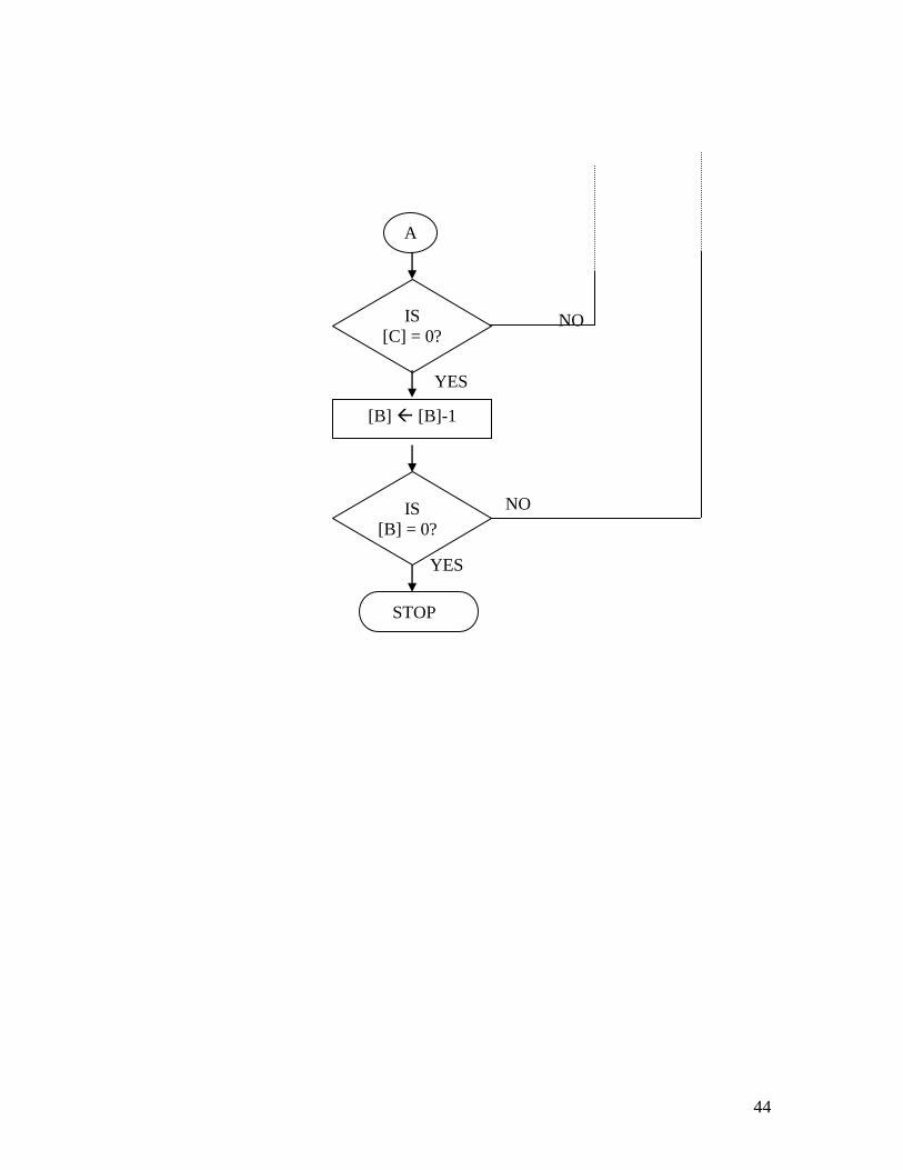
3(A). 8 BIT DATA MULTIPLICATION
AIM:
To multiply two 8 bit numbers stored at consecutive memory locations and store
the result in memory.
ALGORITHM:
LOGIC: Multiplication can be done by repeated addition.
1. Initialize memory pointer to data location.
2. Move multiplicand to a register.
3. Move the multiplier to another register.
4. Clear the accumulator.
5. Add multiplicand to accumulator
6. Decrement multiplier
7. Repeat step 5 till multiplier comes to zero.
8. The result, which is in the accumulator, is stored in a memory location.
RESULT:
Thus the 8-bit multiplication was done in 8085 p using repeated addition method.

12
FLOW CHART:
NO
YES
NO
YES
[HL] 4500
B M
A 00
C 00
Is there
any carry
C C+1
B B-1
[A] [A] +[M]
[HL] [HL]+1
IS B=0
A
START

13
A
STOP
[HL] [HL]+1
[M] [A]
[M] [C]
[HL] [HL]+1
14
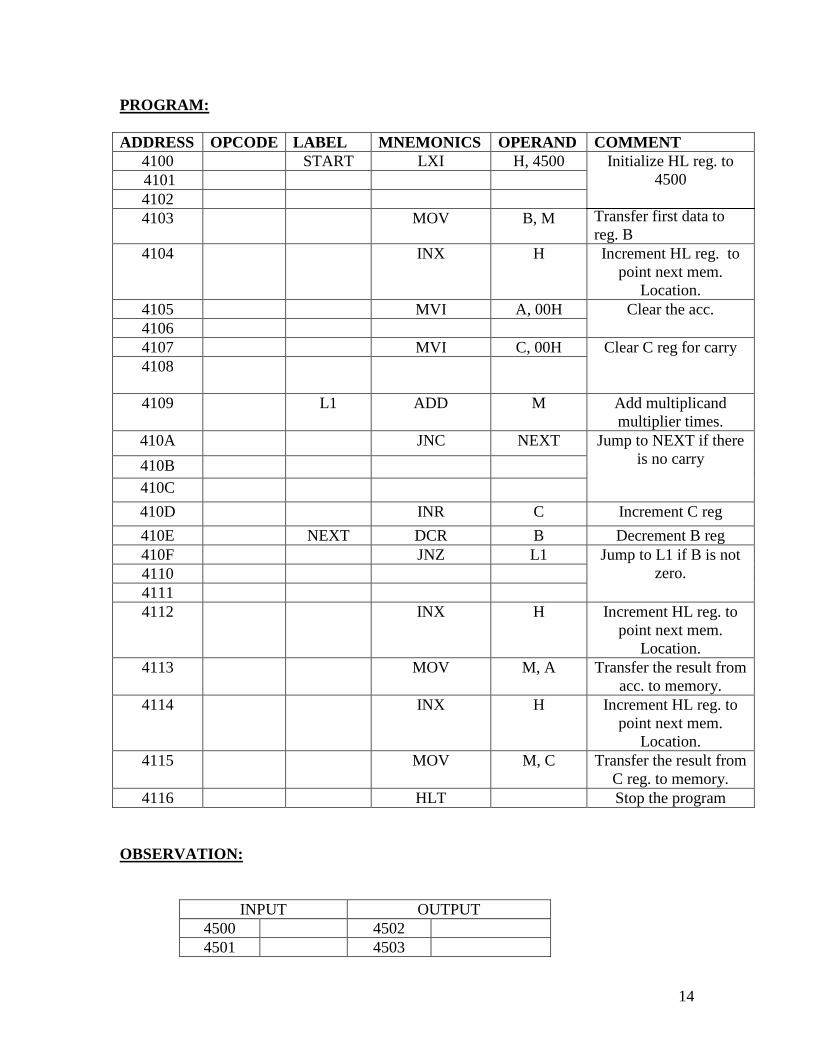
PROGRAM:
ADDRESS OPCODE LABEL MNEMONICS OPERAND COMMENT
4100 START LXI H, 4500 Initialize HL reg. to
4500
Transfer first data to
reg. B
4101
4102
4103 MOV B, M
4104 INX H Increment HL reg. to
point next mem.
Location.
4105 MVI A, 00H Clear the acc.
4106
4107 MVI C, 00H Clear C reg for carry
4108
4109 L1 ADD M Add multiplicand
multiplier times.
410A JNC NEXT Jump to NEXT if there
is no carry 410B
410C
410D INR C Increment C reg
410E NEXT DCR B Decrement B reg
410F JNZ L1 Jump to L1 if B is not
zero. 4110
4111
4112 INX H Increment HL reg. to
point next mem.
Location.
4113 MOV M, A Transfer the result from
acc. to memory.
4114 INX H Increment HL reg. to
point next mem.
Location.
4115 MOV M, C Transfer the result from
C reg. to memory.
4116 HLT Stop the program
OBSERVATION:
INPUT OUTPUT
4500 4502
4501 4503

15
3(B). 8 BIT DIVISION
AIM:
To divide two 8-bit numbers and store the result in memory.
ALGORITHM:
LOGIC: Division is done using the method Repeated subtraction.
1. Load Divisor and Dividend
2. Subtract divisor from dividend
3. Count the number of times of subtraction which equals the quotient
4. Stop subtraction when the dividend is less than the divisor .The dividend now
becomes the remainder. Otherwise go to step 2.
5. stop the program execution.
RESULT:
Thus an ALP was written for 8-bit division using repeated subtraction method and
executed using 8085 p kits

16
FLOWCHART:
NO
YES
B 00
M A-M
[B] [B] +1
IS A<0
A A+ M
B B-1
[HL] 4500
A M
[HL] [HL]+1
START
STOP
[HL] [HL]+1
[M] [A]
[M] [B]
[HL] [HL]+1

17
PROGRAM:
ADDRESS OPCODE LABEL MNEMO
NICS
OPERA
ND
COMMENTS
4100 MVI B,00 Clear B reg for quotient
4101
4102 LXI H,4500 Initialize HL reg. to
4500H 4103
4104
4105 MOV A,M Transfer dividend to acc.
4106 INX H Increment HL reg. to point
next mem. Location.
4107 LOOP SUB M Subtract divisor from dividend
4108 INR B Increment B reg
4109 JNC LOOP Jump to LOOP if result does
not yield borrow 410A
410B
410C ADD M Add divisor to acc.
410D DCR B Decrement B reg
410E INX H Increment HL reg. to point
next mem. Location.
410F MOV M,A Transfer the remainder from
acc. to memory.
4110 INX H Increment HL reg. to point
next mem. Location.
4111 MOV M,B Transfer the quotient from B
reg. to memory.
4112 HLT Stop the program
OBSERVATION:
S.NO INPUT OUTPUT
ADDRESS DATA ADDRESS DATA
1 4500 4502
4501 4503
2 4500 4502
4501 4503

18
4(A). 16 BIT DATA ADDITION
AIM:
To add two 16-bit numbers stored at consecutive memory locations.
ALGORITHM:
1. Initialize memory pointer to data location.
2. Get the first number from memory and store in Register pair.
3. Get the second number in memory and add it to the Register pair.
4. Store the sum & carry in separate memory locations.
RESULT:
Thus an ALP program for 16-bit addition was written and executed in 8085 p
using special instructions.
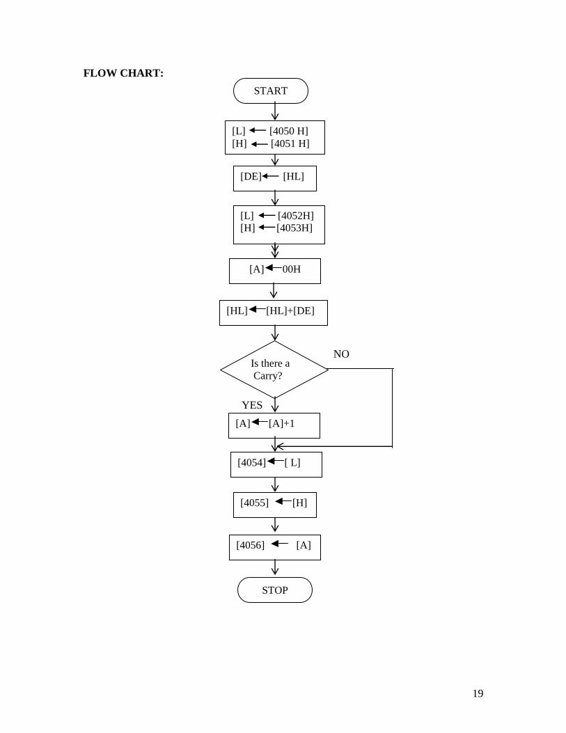
19
FLOW CHART:
NO
YES
START
[DE] [HL]
[L] [4052H]
[H] [4053H]
[A] 00H
[HL] [HL]+[DE]
[L] [4050 H]
[H] [4051 H]
Is there a
Carry?
STOP
[4054] [ L]
[4055] [H]
[A] [A]+1
[4056] [A]

20
PROGRAM:
ADDRESS OPCODE LABEL MNEMONICS OPERAND COMMENT
4000 START LHLD 4050H Load the augend in DE
pair through HL pair. 4001
4002
4003 XCHG
4004 LHLD 4052H Load the addend in HL
pair. 4005
4006
4007 MVI A, 00H Initialize reg. A for
carry 4008
4009 DAD D Add the contents of HL
Pair with that of DE
pair.
400A JNC LOOP If there is no carry, go
to the instruction
labeled LOOP. 400B
400C
400D INR A Otherwise increment
reg. A
400E LOOP SHLD 4054H Store the content of HL
Pair in 4054H(LSB of
sum) 400F
4010
4011 STA 4056H Store the carry in
4056H through Acc.
(MSB of sum). 4012
4013
4014 HLT Stop the program.
OBSERVATION:
INPUT OUTPUT
ADDRESS DATA ADDRESS DATA
4050H 4054H
4051H 4055H
4052H 4056H
4053H

21
4(B). 16 BIT DATA SUBTRACTION
AIM:
To subtract two 16-bit numbers stored at consecutive memory locations.
ALGORITHM:
1. Initialize memory pointer to data location.
2. Get the subtrahend from memory and transfer it to register pair.
3. Get the minuend from memory and store it in another register pair.
4. Subtract subtrahend from minuend.
5. Store the difference and borrow in different memory locations.
RESULT:
Thus an ALP program for subtracting two 16-bit numbers was written and
executed.
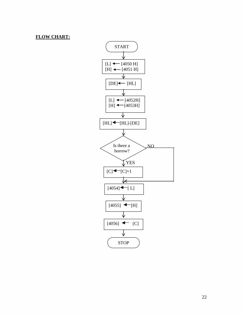
22
FLOW CHART:
NO
YES
START
[DE] [HL]
[L] [4052H]
[H] [4053H]
[HL] [HL]-[DE]
[L] [4050 H]
[H] [4051 H]
Is there a
borrow?
STOP
[4054] [ L]
[4055] [H]
[C] [C]+1
[4056] [C]
23
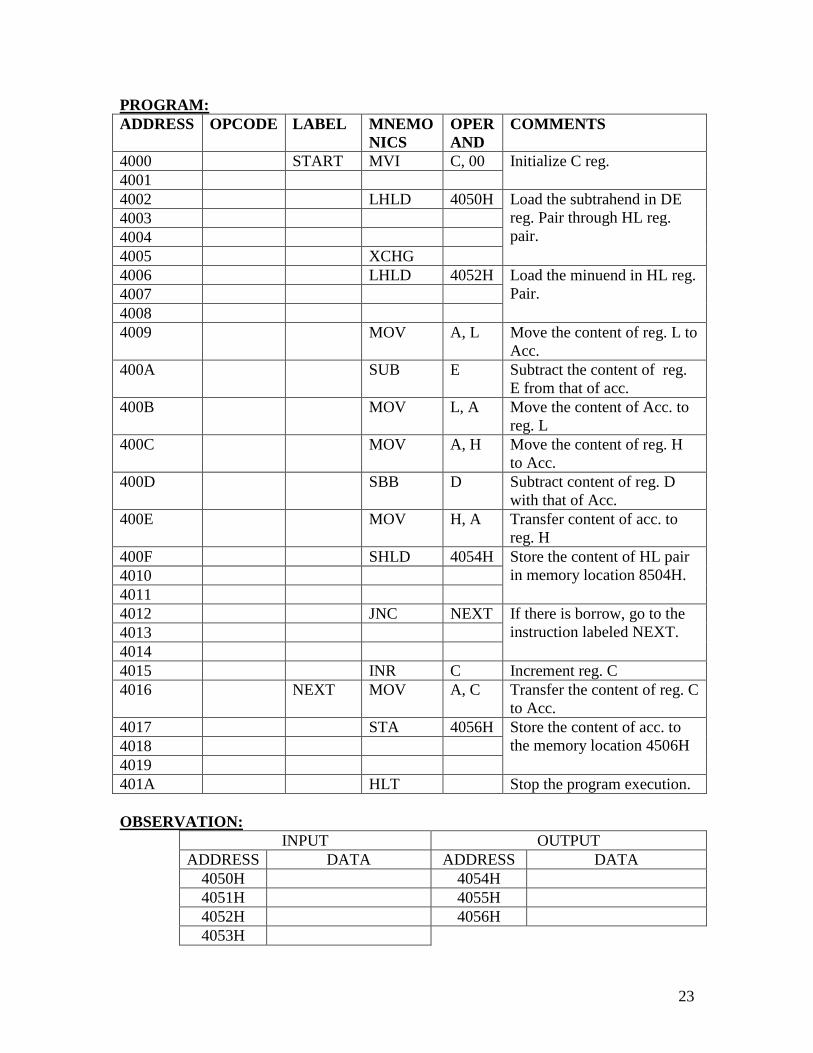
PROGRAM:
ADDRESS OPCODE LABEL MNEMO
NICS
OPER
AND
COMMENTS
4000 START MVI C, 00 Initialize C reg.
4001
4002 LHLD 4050H Load the subtrahend in DE
reg. Pair through HL reg.
pair. 4003
4004
4005 XCHG
4006 LHLD 4052H Load the minuend in HL reg.
Pair. 4007
4008
4009 MOV A, L Move the content of reg. L to
Acc.
400A SUB E Subtract the content of reg.
E from that of acc.
400B MOV L, A Move the content of Acc. to
reg. L
400C MOV A, H Move the content of reg. H
to Acc.
400D SBB D Subtract content of reg. D
with that of Acc.
400E MOV H, A Transfer content of acc. to
reg. H
400F SHLD 4054H Store the content of HL pair
in memory location 8504H. 4010
4011
4012 JNC NEXT If there is borrow, go to the
instruction labeled NEXT. 4013
4014
4015 INR C Increment reg. C
4016 NEXT MOV A, C Transfer the content of reg. C
to Acc.
4017 STA 4056H Store the content of acc. to
the memory location 4506H 4018
4019
401A HLT Stop the program execution.
OBSERVATION:
INPUT OUTPUT
ADDRESS DATA ADDRESS DATA
4050H 4054H
4051H 4055H
4052H 4056H
4053H

24
5(A). 16 BIT MULTIPLICATION
AIM:
To multiply two 16 bit numbers and store the result in memory.
ALGORITHM:
1. Get the multiplier and multiplicand.
2. Initialize a register to store partial product.
3. Add multiplicand, multiplier times.
4. Store the result in consecutive memory locations.
RESULT:
Thus the 16-bit multiplication was done in 8085 p using repeated addition
method.
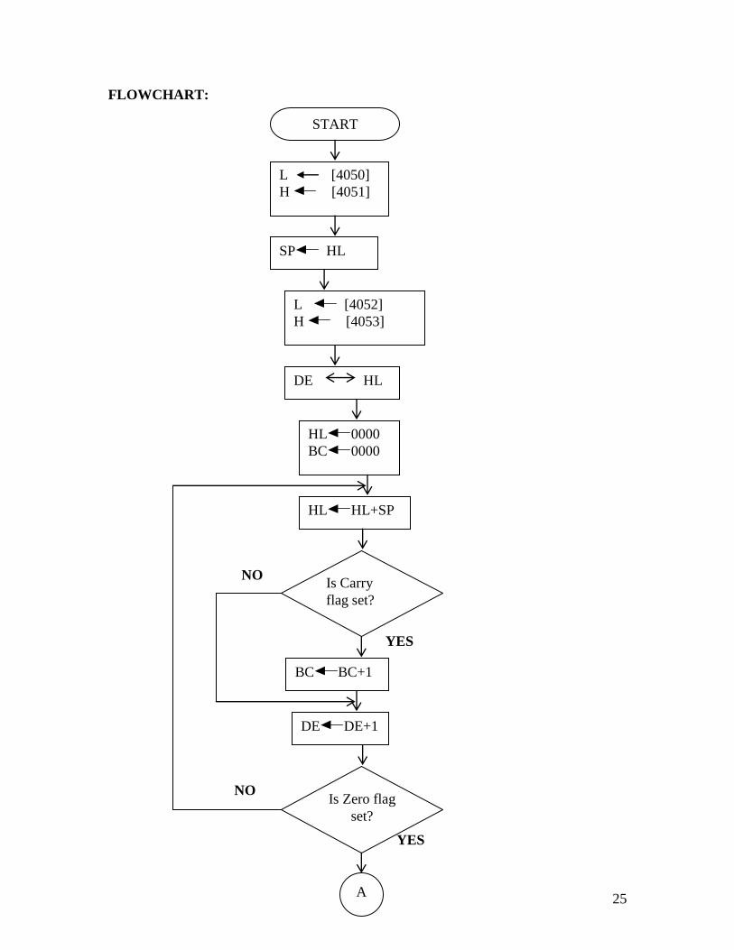
25
FLOWCHART:
NO
YES
NO
YES
START
L [4050]
H [4051]
L [4052]
H [4053]
SP HL
DE HL
HL 0000
BC 0000
HL HL+SP
Is Carry
flag set?
BC BC+1
DE DE+1
Is Zero flag
set?
A

26
A
[4054] L
[4055] H
[4056] C
[4057] B
STOP

27
ADDRESS OPCODE LABEL MNEM
ONICS
OPERAN
D
COMMENTS
8000 START LHLD 4050 Load the first No. in stack pointer
through HL reg. pair 4001
4002
4003 SPHL
4004 LHLD 4052 Load the second No. in HL reg.
pair
& Exchange with DE reg. pair. 4005
4006
4007 XCHG
4008 LXI H, 0000H
Clear HL & DE reg. pairs. 4009
400A
400B LXI B, 0000H
400C
400D
400E LOOP DAD SP Add SP with HL pair.
400F JNC NEXT If there is no carry, go to the
instruction labeled NEXT 4010
4011
4012 INX B Increment BC reg. pair
4013 NEXT DCX D Decrement DE reg. pair.
4014 MOV A,E Move the content of reg. E to Acc.
4015 ORA D OR Acc. with D reg.
4016 JNZ LOOP If there is no zero, go to
instruction labeled LOOP 4017
4018
4019 SHLD 4054 Store the content of HL pair in
memory locations 4054 & 4055. 401A
401B
401C MOV A, C Move the content of reg. C to Acc.
401D STA 4056 Store the content of Acc. in
memory location 4056. 401E
401F
4020 MOV A, B Move the content of reg. B to Acc.
4021 STA 4057 Store the content of Acc. in
memory location 4056. 4022
4023
4024 HLT Stop program execution
OBSERVATION: INPUT OUTPUT
ADDRESS DATA ADDRESS DATA
4050 4054
4051 4055
4052 4056 4053 4057

28
5(B). 16- BIT DIVISION
AIM:
To divide two 16-bit numbers and store the result in memory using 8085
mnemonics.
ALGORITHM:
1. Get the dividend and divisor.
2. Initialize the register for quotient.
3. Repeatedly subtract divisor from dividend till dividend becomes less than divisor.
4. Count the number of subtraction which equals the quotient.
5. Store the result in memory.
RESULT:
Thus the 16-bit Division was done in 8085 p using repeated subtraction method.

29
FLOWCHART:
NO
YES
START
L [4051]
H [4052]
HL DE
L [4050]
H [4051]
BC 0000H
A L; A A- E
L A
A H
A A- H- Borrow
H A
BC BC+ 1
Is Carry
flag set ?
A

30
A
BC BC- 1
HL HL+DE
L [4054]
H [4055]
A C
[4056] A
A B
[4057] A
STOP

31
PROGRAM:
ADDRESS OPCODE LABEL MNEM
ONICS
OPERA
ND
COMMENTS
4000 START LHLD 4052 Load the first No. in stack pointer
through HL reg. pair 4001
4002
4003 XCHG
4004 LHLD 4050 Load the second No. in HL reg. pair
& Exchange with DE reg. pair. 4005
4006
4007 LXI B, 0000H
Clear BC reg. pair. 4008
4009
400A LOOP MOV A, L Move the content of reg. L to Acc.
400B SUB E Subtract reg. E from that of Acc.
400C MOV L, A Move the content of Acc to L.
400D MOV A, H Move the content of reg. H Acc.
400E SBB D Subtract reg. D from that of Acc.
400F MOV H, A Move the content of Acc to H.
4010 INX B Increment reg. Pair BC
4011 JNC LOOP If there is no carry, go to the location
labeled LOOP. 4012
4013
4014 DCX B Decrement BC reg. pair.
4015 DAD D Add content of HL and DE reg. pairs.
4016 SHLD 4054 Store the content of HL pair in 4054 &
4055. 4017
4018
4019 MOV A, C Move the content of reg. C to Acc.
401A STA 4056 Store the content of Acc. in memory
4056 401B
401C
401D MOV A, B Move the content of reg. B to Acc.
401E STA 4057 Store the content of Acc. in memory
4057. 401F
4020
4021 HLT Stop the program execution.
OBSERVATION:
INPUT OUTPUT
ADDRESS DATA ADDRESS DATA
4050 4054
4051 4055
4052 4056
4053 4057

32
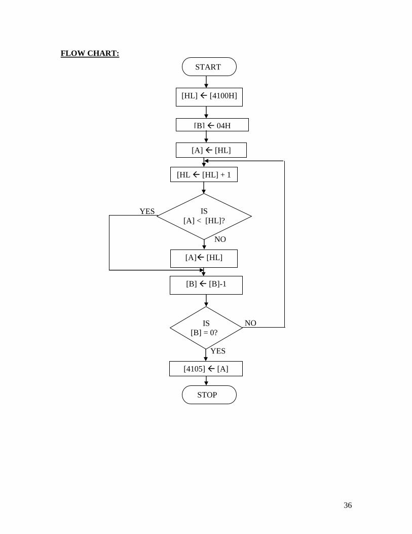
6(A). LARGEST ELEMENT IN AN ARRAY
AIM:
To find the largest element in an array.
ALGORITHM:
1. Place all the elements of an array in the consecutive memory locations.
2. Fetch the first element from the memory location and load it in the accumulator.
3. Initialize a counter (register) with the total number of elements in an array.
4. Decrement the counter by 1.
5. Increment the memory pointer to point to the next element.
6. Compare the accumulator content with the memory content (next
element).
7. If the accumulator content is smaller, then move the memory content
(largest element) to the accumulator. Else continue.
8. Decrement the counter by 1.
9. Repeat steps 5 to 8 until the counter reaches zero
10. Store the result (accumulator content) in the specified memory location.
RESULT:
Thus the largest number in the given array is found out.

33
FLOW CHART:
NO
YES
NO
YES
[B] 04H
[HL] [4100H]
[A] [HL]
[HL [HL] + 1
IS
[A] < [HL]?
[A] [HL]
[4105] [A]
START
[B] [B]-1
IS
[B] = 0?
STOP

34
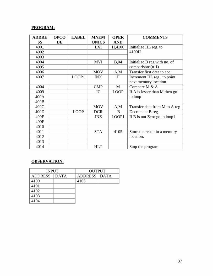
PROGRAM:
ADDRE
SS
OPCO
DE
LABEL MNEM
ONICS
OPER
AND
COMMENTS
4001 LXI H,4100 Initialize HL reg. to
4100H 4002
4003
4004 MVI B,04 Initialize B reg with no. of
comparisons(n-1) 4005
4006 MOV A,M Transfer first data to acc.
4007 LOOP1 INX H Increment HL reg. to point
next memory location
4008 CMP M Compare M & A
4009 JNC LOOP If A is greater than M then go
to loop 400A
400B
400C MOV A,M Transfer data from M to A reg
400D LOOP DCR B Decrement B reg
400E JNZ LOOP1 If B is not Zero go to loop1
400F
4010
4011 STA 4105 Store the result in a memory
location. 4012
4013
4014 HLT Stop the program
OBSERVATION:
INPUT OUTPUT
ADDRESS DATA ADDRESS DATA
4100 4105
4101
4102
4103
4104

35
6(B). SMALLEST ELEMENT IN AN ARRAY
AIM:
To find the smallest element in an array.
ALGORITHM:
1. Place all the elements of an array in the consecutive memory locations.
2. Fetch the first element from the memory location and load it in the accumulator.
3. Initialize a counter (register) with the total number of elements in an array.
4. Decrement the counter by 1.
5. Increment the memory pointer to point to the next element.
6. Compare the accumulator content with the memory content (next
element).
7. If the accumulator content is smaller, then move the memory content
(largest element) to the accumulator. Else continue.
8. Decrement the counter by 1.
9. Repeat steps 5 to 8 until the counter reaches zero
10. Store the result (accumulator content) in the specified memory location.
RESULT:
Thus the smallest number in the given array is found out.
36
FLOW CHART:
YES
NO
NO
YES
[B] 04H
[HL] [4100H]
[A] [HL]
[HL [HL] + 1
IS
[A] < [HL]?
[A] [HL]
[4105] [A]
START
[B] [B]-1
IS
[B] = 0?
STOP
37
PROGRAM:
ADDRE
SS
OPCO
DE
LABEL MNEM
ONICS
OPER
AND
COMMENTS
4001 LXI H,4100 Initialize HL reg. to
4100H 4002
4003
4004 MVI B,04 Initialize B reg with no. of
comparisons(n-1) 4005
4006 MOV A,M Transfer first data to acc.
4007 LOOP1 INX H Increment HL reg. to point
next memory location
4004 CMP M Compare M & A
4009 JC LOOP If A is lesser than M then go
to loop 400A
400B
400C MOV A,M Transfer data from M to A reg
400D LOOP DCR B Decrement B reg
400E JNZ LOOP1 If B is not Zero go to loop1
400F
4010
4011 STA 4105 Store the result in a memory
location. 4012
4013
4014 HLT Stop the program
OBSERVATION:
INPUT OUTPUT
ADDRESS DATA ADDRESS DATA
4100 4105
4101
4102
4103
4104

38
7(A).ASCENDING ORDER
AIM:
To sort the given number in the ascending order using 8085 microprocessor.
ALGORITHM:
1. Get the numbers to be sorted from the memory locations.
2. Compare the first two numbers and if the first number is larger than second then I
interchange the number.
3. If the first number is smaller, go to step 4
4. Repeat steps 2 and 3 until the numbers are in required order
RESULT:
Thus the ascending order program is executed and thus the numbers are arranged
in ascending order.

39
FLOWCHART:
YES
NO
[B] 04H
[HL] [4100H]
[A] [HL]
[HL [HL] + 1
IS
[A] < [HL]?
[D] [HL]
[HL] [A]
[HL] [HL] - 1
[HL] [D]
[HL] [HL] + 1
[C] [C] – 01 H
A
[C] 04H
START

40
NO
YES
NO
YES
IS
[C] = 0?
A
[B] [B]-1
IS
[B] = 0?
STOP

41
PROGRAM:
ADDR
E
SS
OPCO
DE
LABEL MNEM
ONICS
OPER
AND
COMMENTS
4000 MVI B,04 Initialize B reg with number
of comparisons (n-1) 4001
4002 LOOP 3 LXI H,4100 Initialize HL reg. to
4100H 4003
4004
4005 MVI C,04 Initialize C reg with no. of
comparisons(n-1) 4006
4007 LOOP2 MOV A,M Transfer first data to acc.
4004 INX H Increment HL reg. to point
next memory location
4009 CMP M Compare M & A
400A JC LOOP1 If A is less than M then go to
loop1 400B
400C
400D MOV D,M Transfer data from M to D reg
400E MOV M,A Transfer data from acc to M
400F DCX H Decrement HL pair
4010 MOV M,D Transfer data from D to M
4011 INX H Increment HL pair
4012 LOOP1 DCR C Decrement C reg
4013 JNZ LOOP2 If C is not zero go to loop2
4014
4015
4016 DCR B Decrement B reg
4017 JNZ LOOP3 If B is not Zero go to loop3
4014
4019
401A HLT Stop the program
OBSERVATION:
INPUT OUTPUT
MEMORY
LOCATION
DATA MEMORY
LOCATION
DATA
4100 4100
4101 4101
4102 4102
4103 4103
4104 4104

42
7(B). DESCENDING ORDER
AIM:
To sort the given number in the descending order using 8085 microprocessor.
ALGORITHM:
1. Get the numbers to be sorted from the memory locations.
2. Compare the first two numbers and if the first number is smaller than second then I
interchange the number.
3. If the first number is larger, go to step 4
4. Repeat steps 2 and 3 until the numbers are in required order
RESULT:
Thus the descending order program is executed and thus the numbers are arranged
in descending order.

43
FLOWCHART:
NO
YES
[B] 04H
[HL] [4100H]
[A] [HL]
[HL [HL] + 1
IS
[A] < [HL]?
[D] [HL]
[HL] [A]
[HL] [HL] - 1
[HL] [D]
[HL] [HL] + 1
[C] [C] – 01 H
A
[C] 04H
START
44
NO
YES
NO
YES
IS
[C] = 0?
A
[B] [B]-1
IS
[B] = 0?
STOP

45
PROGRAM:
ADDRE
SS
OPCO
DE
LABEL MNEM
ONICS
OPER
AND
COMMENTS
4000 MVI B,04 Initialize B reg with number
of comparisons (n-1) 4001
4002 LOOP 3 LXI H,4100 Initialize HL reg. to
4100H 4003
4004
4005 MVI C,04 Initialize C reg with no. of
comparisons(n-1) 4006
4007 LOOP2 MOV A,M Transfer first data to acc.
4004 INX H Increment HL reg. to point
next memory location
4009 CMP M Compare M & A
400A JNC LOOP1 If A is greater than M then go
to loop1 400B
400C
400D MOV D,M Transfer data from M to D reg
400E MOV M,A Transfer data from acc to M
400F DCX H Decrement HL pair
4010 MOV M,D Transfer data from D to M
4011 INX H Increment HL pair
4012 LOOP1 DCR C Decrement C reg
4013 JNZ LOOP2 If C is not zero go to loop2
4014
4015
4016 DCR B Decrement B reg
4017 JNZ LOOP3 If B is not Zero go to loop3
4014
4019
401A HLT Stop the program
OBSERVATION:
INPUT OUTPUT
MEMORY
LOCATION
DATA MEMORY
LOCATION
DATA
4100 4100
4101 4101
4102 4102
4103 4103
4104 4104

46
8. BIOS/DOS CALLS – DISPLAY
AIM:
To display a message on the CRT screen of a microcomputer using DOS calls.
ALGORITHM:
1. Initialize the data segment and the message to be displayed.
2. Set function value for display.
3. Point to the message and run the interrupt to display the message in the CRT.
PROGRAM:
ASSUME CS: CODE, DS: DATA
DATA SEGMENT
MSG DB 0DH, 0AH, “GOOD MORNING” , ODH, OAH, “$”
DATA ENDS
CODE SEGMENT
START: MOV AX, DATA
MOV DS, AX
MOV AH, 09H
MOV DX, OFFSET MSG
INT 21H
MOV AH, 4CH
INT 21H
CODE ENDS
END START
RESULT:
A message is displayed on the CRT screen of a microcomputer using DOS calls
47
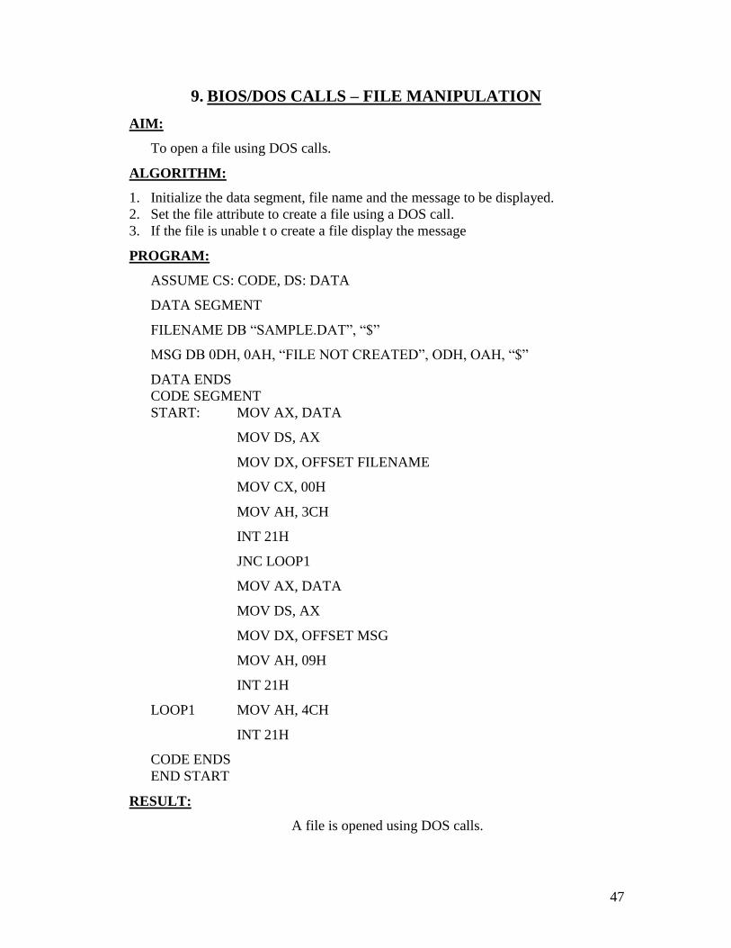
9. BIOS/DOS CALLS – FILE MANIPULATION
AIM:
To open a file using DOS calls.
ALGORITHM:
1. Initialize the data segment, file name and the message to be displayed.
2. Set the file attribute to create a file using a DOS call.
3. If the file is unable t o create a file display the message
PROGRAM:
ASSUME CS: CODE, DS: DATA
DATA SEGMENT
FILENAME DB “SAMPLE.DAT”, “$”
MSG DB 0DH, 0AH, “FILE NOT CREATED”, ODH, OAH, “$”
DATA ENDS
CODE SEGMENT
START: MOV AX, DATA
MOV DS, AX
MOV DX, OFFSET FILENAME
MOV CX, 00H
MOV AH, 3CH
INT 21H
JNC LOOP1
MOV AX, DATA
MOV DS, AX
MOV DX, OFFSET MSG
MOV AH, 09H
INT 21H
LOOP1 MOV AH, 4CH
INT 21H
CODE ENDS
END START
RESULT:
A file is opened using DOS calls.

48
10. BIOS/DOS CALLS – DISK INFORMATION
AIM:
To display the disk information.
ALGORITHM:
1. Initialize the data segment and the message to be displayed.
2. Set function value for disk information.
3. Point to the message and run the interrupt to display the message in the CRT.
PROGRAM:
ASSUME CS: CODE, DS: DATA
DATA SEGMENT
MSG DB 0DH, 0AH, “GOOD MORNING” , ODH, OAH, “$”
DATA ENDS
CODE SEGMENT
START: MOV AX, DATA
MOV DS, AX
MOV AH, 36H
MOV DX, OFFSET MSG
INT 21H
MOV AH, 4CH
INT 21H
CODE ENDS
END START
RESULT:
The disk information is displayed.
49
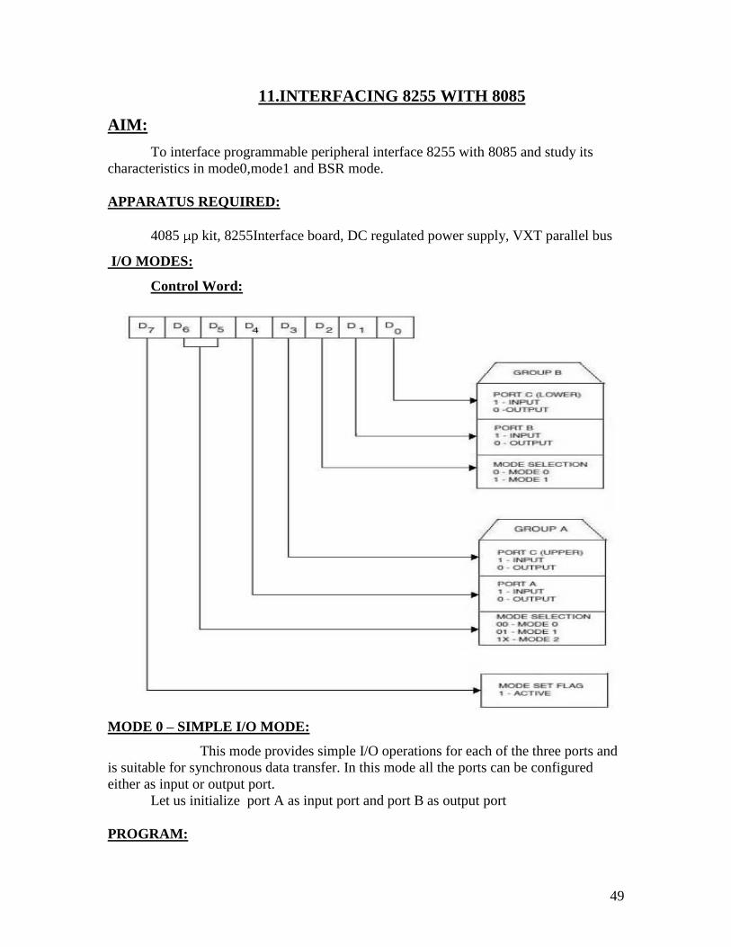
11.INTERFACING 8255 WITH 8085
AIM:
To interface programmable peripheral interface 8255 with 8085 and study its
characteristics in mode0,mode1 and BSR mode.
APPARATUS REQUIRED:
4085 p kit, 8255Interface board, DC regulated power supply, VXT parallel bus
I/O MODES:
Control Word:
MODE 0 – SIMPLE I/O MODE:
This mode provides simple I/O operations for each of the three ports and
is suitable for synchronous data transfer. In this mode all the ports can be configured
either as input or output port.
Let us initialize port A as input port and port B as output port
PROGRAM:

50
ADDRESS OPCODES LABEL MNEMONICS OPERAND COMMENTS
4100 START: MVI A, 90 Initialize port A
as Input and Port
B as output. 4101
4102 OUT C6 Send Mode
Control word 4103
4104 IN C0 Read from Port A
4105
4106 OUT C2 Display the data
in port B 4107
4108 STA 4200 Store the data
read from Port A
in 4200 4109
410A
410B HLT Stop the
program.
MODE1 STROBED I/O MODE:
In this mode, port A and port B are used as data ports and port C is used as control
signals for strobed I/O data transfer.
Let us initialize port A as input port in mode1
MAIN PROGRAM:
ADDRESS OPCODES LABEL MNEMONICS OPERAND COMMENTS
4100 START: MVI A, B4 Initialize port A
as Input port in
mode 1. 4101
4102 OUT C6 Send Mode
Control word 4103
4104 MVI A,09 Set the PC4 bit
for INTE A
4105
4106 OUT C6 Display the data
in port B
4107
EI
4108 MVI A,08 Enable RST5.5
4109
410A SIM
EI
410B HLT Stop the
program.
ISR (Interrupt Service Routine)

51
ADDRESS OPCODES LABEL MNEMONICS OPERAND COMMENTS
4200 START: IN C0 Read from port A
4201
4202 STA 4500 Store in 4500.
4203
4204
4205 HLT Stop the
program.
Sub program:
ADDRESS OPCODES LABEL MNEMONICS OPERAND COMMENTS
405E JMP 4200 Go to 4200
405F
4060
BSR MODE (Bit Set Reset mode)
Any lines of port c can be set or reset individually without affecting other lines
using this mode. Let us set PC0 and PC3 bits using this mode.

52
PROGRAM:
ADDRESS OPCODES LABEL MNEMONICS OPERAND COMMENTS
4100 START: MVI A, 01 Set PC0
4101
4102 OUT C6 Send Mode
Control word 4103
4104 MVI A,07 Set PC3
4105
4106 OUT C6 Send Mode
Control word 4107
4109 HLT Stop the
program.
RESULT:
Thus 8255 is interfaced and its characteristics in mode0,mode1 and BSR mode is
studied.

53
12. INTERFACING 8253 TIMER WITH 8085
Interfacing 8253 Programmable Interval Timer with 8085 p
AIM:
To interface 8253 Interface board to 8085 p and to generate a square wave of
150MHz.
APPARATUS REQUIRED:
8085 p kit, 8253 Interface board, DC regulated power supply, VXT parallel bus,
CRO.
Mode 3 Square wave generator:
It is similar to Mode 2 except that the output will remain high until one half of count
and go low for the other half for even number count. If the count is odd, the output
will be high for (count + 1)/2 counts. This mode is used of generating Baud rate for
8251A (USART).
Example:
We utilize Mode 0 to generate a square wave of frequency 150 KHz at channel 0.
Address Opcodes Label Mnemonic Operands Comments
4100 3E 36 START: MVI A, 36 Channel 0 in mode 3
4102 D3 CE OUT CE Send Mode Control word
4104 3E 0A MVI A, 0A LSB of count
4106 D3 C8 OUT C8 Write count to register
4108 3E 00 MVI A, 00 MSB of count
410A D3 C8 OUT C8 Write count to register
410C 76 HLT
Set the jumper, so that the clock 0 of 8253 is given a square wave of frequency 1.5 MHz.
This program divides this PCLK by 10 and thus the output at channel 0 is 150 KHz.
Vary the frequency by varying the count. Here the maximum count is FFFF H.
So, the square wave will remain high for 7FFF H counts and remain low for 7FFF H
counts. Thus with the input clock frequency of 1.5 MHz, which corresponds to a period
of 0.067 microseconds, the resulting square wave has an ON time of 0.02184
microseconds and an OFF time of 0.02184 microseconds.
To increase the time period of square wave, set the jumpers such that CLK2 of
8253 is connected to OUT 0. Using the above-mentioned program, output a square wave
of frequency 150 KHz at channel 0. Now this is the clock to channel 2.
Result:
Thus the 8253 has been interfaced with 8085 p to generate a Square Wave of
150KHz
54
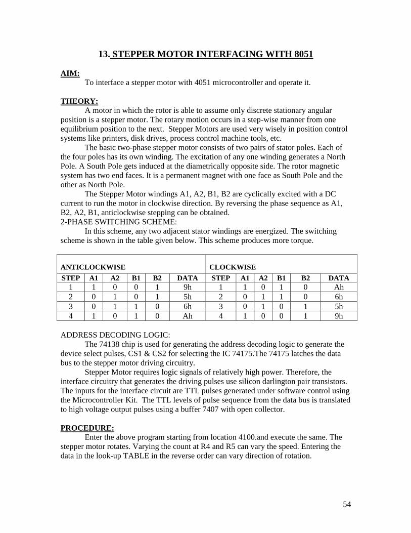
13. STEPPER MOTOR INTERFACING WITH 8051
AIM:
To interface a stepper motor with 4051 microcontroller and operate it.
THEORY:
A motor in which the rotor is able to assume only discrete stationary angular
position is a stepper motor. The rotary motion occurs in a step-wise manner from one
equilibrium position to the next. Stepper Motors are used very wisely in position control
systems like printers, disk drives, process control machine tools, etc.
The basic two-phase stepper motor consists of two pairs of stator poles. Each of
the four poles has its own winding. The excitation of any one winding generates a North
Pole. A South Pole gets induced at the diametrically opposite side. The rotor magnetic
system has two end faces. It is a permanent magnet with one face as South Pole and the
other as North Pole.
The Stepper Motor windings A1, A2, B1, B2 are cyclically excited with a DC
current to run the motor in clockwise direction. By reversing the phase sequence as A1,
B2, A2, B1, anticlockwise stepping can be obtained.
2-PHASE SWITCHING SCHEME:
In this scheme, any two adjacent stator windings are energized. The switching
scheme is shown in the table given below. This scheme produces more torque.
ANTICLOCKWISE CLOCKWISE
STEP A1 A2 B1 B2 DATA STEP A1 A2 B1 B2 DATA
1 1 0 0 1 9h 1 1 0 1 0 Ah
2 0 1 0 1 5h 2 0 1 1 0 6h
3 0 1 1 0 6h 3 0 1 0 1 5h
4 1 0 1 0 Ah 4 1 0 0 1 9h
ADDRESS DECODING LOGIC:
The 74138 chip is used for generating the address decoding logic to generate the
device select pulses, CS1 & CS2 for selecting the IC 74175.The 74175 latches the data
bus to the stepper motor driving circuitry.
Stepper Motor requires logic signals of relatively high power. Therefore, the
interface circuitry that generates the driving pulses use silicon darlington pair transistors.
The inputs for the interface circuit are TTL pulses generated under software control using
the Microcontroller Kit. The TTL levels of pulse sequence from the data bus is translated
to high voltage output pulses using a buffer 7407 with open collector.
PROCEDURE:
Enter the above program starting from location 4100.and execute the same. The
stepper motor rotates. Varying the count at R4 and R5 can vary the speed. Entering the
data in the look-up TABLE in the reverse order can vary direction of rotation.
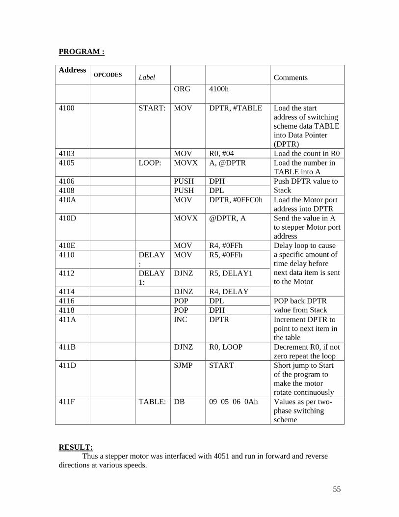
55
PROGRAM :
Address OPCODES Label
Comments
ORG 4100h
4100
START: MOV DPTR, #TABLE Load the start
address of switching
scheme data TABLE
into Data Pointer
(DPTR)
4103 MOV R0, #04 Load the count in R0
4105
LOOP: MOVX A, @DPTR Load the number in
TABLE into A
4106 PUSH DPH Push DPTR value to
Stack 4108 PUSH DPL
410A
MOV DPTR, #0FFC0h Load the Motor port
address into DPTR
410D
MOVX @DPTR, A Send the value in A
to stepper Motor port
address
410E MOV R4, #0FFh Delay loop to cause
a specific amount of
time delay before
next data item is sent
to the Motor
4110
DELAY
:
MOV R5, #0FFh
4112
DELAY
1:
DJNZ R5, DELAY1
4114 DJNZ R4, DELAY
4116 POP DPL POP back DPTR
value from Stack 4118 POP DPH
411A
INC DPTR Increment DPTR to
point to next item in
the table
411B
DJNZ R0, LOOP Decrement R0, if not
zero repeat the loop
411D
SJMP START Short jump to Start
of the program to
make the motor
rotate continuously
411F
TABLE: DB 09 05 06 0Ah Values as per two-
phase switching
scheme
RESULT:
Thus a stepper motor was interfaced with 4051 and run in forward and reverse
directions at various speeds.