Critical Reliability Challenges for The International ... · PDF fileCritical Reliability...
48
Critical Reliability Challenges for The International Technology Roadmap for Semiconductors (ITRS) International SEMATECH Technology Transfer #03024377A-TR
Transcript of Critical Reliability Challenges for The International ... · PDF fileCritical Reliability...

Critical Reliability Challenges for The International Technology Roadmap for Semiconductors (ITRS)
International SEMATECH Technology Transfer #03024377A-TR
© 2003 International SEMATECH, Inc.
International SEMATECH and the International SEMATECH logo are registered service marks of International
SEMATECH, Inc., a wholly-owned subsidiary of SEMATECH, Inc.
Product names and company names used in this publication are for identification purposes only and may be trademarks or service marks of their respective companies.

Critical Reliability Challenges for The International Technology Roadmap for Semiconductors (ITRS)
Technology Transfer #03024377A-TR International SEMATECH
March 31, 2003
Abstract: This white paper highlights the critical near-term reliability challenges facing the International Technology Roadmap for Semiconductors (ITRS). It is intended to help ISMT groups working on the 2003 edition of the ITRS understand why each of these challenges is considered critical and, more importantly, what questions researchers must answer to prevent these issues from blocking manufacturable solutions.
Keywords: Reliability, Planning, Technology Trends
Authors: Richard Blish, Ted Dellin, Steve Huber, Martin Johnson, Jose Maiz, Bob Likins, Nick Lycoudes, Joe McPherson, Yeng Peng, Carl Peridier, Andreas Preussger, George Prokop, and Larry Tullos
Approvals: Noel Durrant, Program Manager, Quality Council Dave Anderson, Director, Corporate Relations Laurie Modrey, Technical Information Transfer Team Leader


iii
International SEMATECH Technology Transfer #03024377A-TR
Table of Contents
1 EXECUTIVE SUMMARY .................................................................................................1
2 INTRODUCTION ..............................................................................................................1
3 DIFFICULT CHALLENGES..............................................................................................3
4 HIGH-k GATE DIELECTRICS ..........................................................................................4 4.1 Challenges .................................................................................................................4 4.2 Paramount Reliability Concerns.................................................................................5 4.3 Research Needs and Questions ..................................................................................5
4.3.1 Material Properties For Front End Processing.................................................5 4.3.2 Failure Modes and Mechanisms .....................................................................5 4.3.3 Physical Model and Model Parameters...........................................................6 4.3.4 Statistical Model ............................................................................................6 4.3.5 Test Methods and Lifetime Prediction............................................................6
4.4 Reliability Metrics .....................................................................................................6 5 METAL GATES..................................................................................................................7
5.1 Challenges .................................................................................................................7 5.2 Paramount Reliability Concerns.................................................................................7 5.3 Research Needs and Questions ..................................................................................7
5.3.1 Materials-Related Needs and Questions .........................................................7 5.3.2 Metal Gate Process Selection Issues ...............................................................8 5.3.3 Stability Related Needs and Questions for Metal Gates ..................................9
5.4 Reliability Metrics .....................................................................................................9 5.5 Effect of Metal Gates on the Reliability Physics ........................................................9
6 COPPER/LOW-k INTERCONNECTS .............................................................................10 6.1 Challenges ...............................................................................................................10 6.2 Paramount Reliability Concerns...............................................................................10 6.3 Research Needs and Questions ................................................................................11
6.3.1 Material Properties.......................................................................................11 6.3.2 Failure Modes and Mechanisms ...................................................................12 6.3.3 Physical Model and Model Parameters.........................................................13 6.3.4 Test Structures and Methods ........................................................................13 6.3.5 Stability of Parameters as Function of Stress and Time.................................14
6.4 Reliability Metrics ...................................................................................................14
7 SILICON ON INSULATOR (SOI)....................................................................................14 7.1 Challenges ...............................................................................................................14 7.2 Paramount Reliability Concerns...............................................................................15 7.3 Research Needs and Questions ................................................................................15
7.3.1 Material Properties.......................................................................................15 7.3.2 Configuration and Organization ...................................................................16 7.3.3 Failure Modes and Mechanisms ...................................................................16 7.3.4 Statistical Models.........................................................................................17 7.3.5 Test Structures .............................................................................................17 7.3.6 Stability of Parameters as a Function of Stress and Time ..............................17
7.4 Reliability Metrics ...................................................................................................17

iv
Technology Transfer #03024377A-TR International SEMATECH
8 NOVEL DEVICES ...........................................................................................................17 8.1 Challenges ...............................................................................................................17 8.2 Paramount Reliability Concerns...............................................................................18 8.3 Research Needs and Questions ................................................................................18
9 MICROSYSTEMS ...........................................................................................................19 9.1 Challenges ...............................................................................................................19 9.2 Paramount Reliability Concerns...............................................................................19 9.3 Research Needs and Questions ................................................................................20
9.3.1 MEMS .........................................................................................................20 9.3.2 Sensors ........................................................................................................20 9.3.3 Integrated Optoelectronics............................................................................20
10 FLASH MEMORIES........................................................................................................21 10.1 Challenges ...............................................................................................................21 10.2 Paramount Reliability Concerns...............................................................................21 10.3 Reliability Requirements and Research Needs .........................................................21
10.3.1 Data Retention .............................................................................................21 10.3.2 Endurance ....................................................................................................22 10.3.3 Multi-Level Cell in a Single Flash Transistor ...............................................22 10.3.4 Design..........................................................................................................22 10.3.5 Testing .........................................................................................................22
10.4 Reliability Metrics ...................................................................................................22 11 SOFT ERRORS................................................................................................................23
11.1 Challenges ...............................................................................................................23 11.2 Paramount Reliability Concerns...............................................................................23 11.3 Research Needs and Questions ................................................................................24
11.3.1 Memories.....................................................................................................24 11.3.2 Logic Components and Systems...................................................................24 11.3.3 Materials ......................................................................................................24 11.3.4 Models and Simulation.................................................................................25
11.4 Reliability Metrics ...................................................................................................25 12 ELECTROSTATIC DISCHARGE PROTECTION ...........................................................25
12.1 Challenges ...............................................................................................................25 12.2 Paramount Reliability Concerns...............................................................................26 12.3 Research Needs and Questions ................................................................................26 12.4 Reliability Metrics ...................................................................................................26
13 LATCHUP........................................................................................................................27 13.1 Challenges ...............................................................................................................27 13.2 Paramount Reliability Concerns...............................................................................27 13.3 Research Needs and Questions ................................................................................27
14 IMPACT OF SCALING ON PACKAGING......................................................................28 14.1 Challenges ...............................................................................................................28 14.2 Paramount Reliability Concerns...............................................................................29 14.3 Research Needs and Questions ................................................................................30
14.3.1 Materials Properties .....................................................................................30 14.3.2 Failure Modes and Mechanisms ...................................................................30 14.3.3 Physical Models and Model Parameters .......................................................30

v
International SEMATECH Technology Transfer #03024377A-TR
14.3.4 Test Structures .............................................................................................30 15 DESIGN FOR RELIABILITY (DFR) ...............................................................................31
15.1 Challenges ...............................................................................................................31 15.2 Paramount Needs.....................................................................................................32 15.3 Research Needs and Questions ................................................................................32
15.3.1 CAD Tool and Data Interface.......................................................................32 15.3.2 Reliability Point CAD Solutions – Standalone Tools ....................................32
16 IMPACT OF DEFECT SCREENING ON DEVICE RELIABILITY.................................33 16.1 Challenges ...............................................................................................................33 16.2 Paramount Reliability Concerns...............................................................................35 16.3 Research Needs and Questions ................................................................................35
16.3.1 Defect Properties..........................................................................................35 16.3.2 Failure Modes and Mechanisms ...................................................................35 16.3.3 Physical Models and Model Parameters .......................................................36 16.3.4 Statistical Models.........................................................................................36 16.3.5 Latent Defect Screens (Detection Methods)..................................................36 16.3.6 Test Structures .............................................................................................36 16.3.7 Stability of Parameters as a Function of Stress and Time ..............................36
16.4 Reliability Metrics ...................................................................................................37
List of Tables
Table 1 Difficult Challenges ...............................................................................................3

vi
Technology Transfer #03024377A-TR International SEMATECH
Acknowledgments
Contributors to this report included the following members of the ISMT Reliability Technology Advisory Board:
Rod Augur, Philips Semiconductors
Richard Blish, Advanced Micro Devices
Ted Dellin, Sandia National Labs
Bill End, Advanced Micro Devices
Steve Huber, Intel Corp.
Martin Johnson, Philips Semiconductors
Seung Kang, Agere Systems
Andreas Kerber, Infineon Technologies
Pon Ku, Motorola
Bob Likins, Advanced Micro Devices
Nick Lycoudes, Motorola
Jose Maiz, Intel Corp.
Joe McPherson, Texas Instruments
Yeng Peng, Taiwan Semiconductor Manufacturing Co.
Carl Peridier, Agere Systems
Andreas Preussger, Infineon Technologies
George Prokop, IBM Microelectronics
Larry Tullos, STMicroelectronics
Ken Wu, Taiwan Semiconductor Manufacturing Co.

1
International SEMATECH Technology Transfer #03024377A-TR
1 EXECUTIVE SUMMARY
This document highlights the principal reliability challenges associated with key semiconductor technologies and identifies the research needs to assess and control the reliability risks.
Based upon the consensus of the Reliability Technical Advisory Board (RTAB), the top five issues that deserve the most attention are high-k gate dielectrics, metal gate, copper/low-k interconnects, packaging, and design and test for reliability.
Within high-k gate dielectrics, metal gate, copper/low-k interconnects, the introduction of new materials, processes, and devices presents challenges. Bulk material and interface properties usually define the intrinsic reliability characteristics while defects establish the extrinsic reliability characteristics. Process integration flow, techniques, and process tools often create first order reliability effects (both intrinsic and extrinsic). The importance of characterizing these materials and processes for reliability as well as for performance during the early development stage cannot be overstated.
System-on-chip (SOC) products that typically integrate new function and often include large memories (SRAM, DRAM, and Flash) bring about unique design, integration, and test challenges. Microsystems require consideration of a wider range of failure modes than microelectronics alone and introduce new failure modes because of the interaction of diverse technologies that would not be present if each technology were manufactured on a separate chip. In addition, optical, chemical, and biometric sensors and micromachines (MEMs) require the development of new accelerated tests and failure mechanism models.
Electrostatic discharge (ESD), latchup, and packaging in the nanometer regime also raise reliability concerns. Even though ESD and latchup effects have been well characterized for many years, scaling brings about new issues and concerns. Similarly, the increased complexity and performance requirements for packaging these products act as an exponential multiplier for many of the failure mechanisms besides introducing new ones.
Finally, two critical crosscut issues are related to design and test. These may be the more difficult challenges as the work needed to reach solutions is typically dispersed across many organizations, sites, and partners. Integration efforts tend to be less focused than material and device issues. Although the challenges may be clear, the paths to find solutions tend to be fragmented and obscure; consequently, these items require special research focus.
This document is neither a complete nor exhaustive list of reliability challenges for the ITRS. Certainly any area of technology advancement includes its own set of potential reliability problems and new challenges. Instead, those broadest or most critical challenges are highlighted. It is hoped that this document can provide perspective and guidance as well as improve the dialog with other technologists working to develop the 2003 edition of the ITRS.
2 INTRODUCTION
Clearly, the development of semiconductor technology in the next 7 years will bring a broad set of reliability challenges at a pace that has not been seen in the last 30 years. Many aspects of semiconductor design and manufacturing will undergo dramatic changes that threaten the nearly unlimited lifetime and high level of reliability that customers have come to expect even as product complexity and performance have increased. The introduction of new materials, processes, and novel devices along with voltage scaling limitations, increasing power, die size,

2
Technology Transfer #03024377A-TR International SEMATECH
and package complexity will impose many new reliability challenges. Product cost and performance requirements will be substantially affected and, in many cases, superseded by reliability constraints. Perhaps the greatest challenge is that all of these changes must occur without the benefit of the extended learning that has sustained this industry in the past.
Two other trends are also forcing a dramatic change in the approach and methods for assuring product reliability. First, the gap between normal operating and accelerated test conditions is continuing to narrow, reducing the acceleration factors. Second, increased device complexity is making it impossible or prohibitively expensive to exercise or stimulate the product to obtain sufficient fault coverage in accelerated life tests. As a result, the efficiency and even the ability to meaningfully test reliability at the product level are rapidly diminishing.
As the market demand continues to push product performance to its technological limits, the tradeoff between performance and lifetime must be tailored to the needs of different market segments. No longer can a single product satisfy all applications with significant reliability and performance margins. This in turn requires that accurate reliability models and tools for lifetime estimation must be available during the product design stage. A failure mechanism-driven approach must be employed, identifying the potential failures and evaluating their kinetics and impact based on the specific application conditions and requirements of each market segment. A much improved understanding of materials properties and failure mechanisms and models is required. If decisions rely on standards-based tests, then performance may be artificially limited and/or development costs increased while driving reliability to levels beyond the product or application needs. Together these trends demand that reliability be modeled much more precisely during the product design cycle to make the correct performance vs. reliability tradeoffs. This in turn requires that the following be in place:
• Well developed physical models for failure mechanisms
• Understanding of the variation to apply correct statistical models
• Test methods and test structures to fully characterize each failure mechanism
• Design tools to transform the test structure reliability predictions for individual failure mechanisms to a comprehensive product reliability model that fits the application operating conditions and environment
To increase the rate of acceptance of model-based reliability, industry-accepted guidelines for reliability modeling are needed. Making decisions on standards-based tests and readouts risks building in excessive reliability at the expense of performance and cost or failure resulting from mismatched tests and segment application.
The introduction of new materials with more limited operating margins further accelerates this shift and requires that the potential failure mechanisms, the required test structures, and the corresponding models be identified and developed well in advance of the technology qualification. Similarly, the introduction of novel devices and new components for SOC integration will have profound reliability impacts as they bring new failure modes and mechanisms. Many of these devices are now in their infancy, and practical devices are still too far away for reliability characterization. If history is a guide, it is likely that work on the reliability of these novel devices will be late and sub-critical. Bringing reliability issues upstream in the development process will result in a better assessment of the readiness of these technologies for volume production.

3
International SEMATECH Technology Transfer #03024377A-TR
3 DIFFICULT CHALLENGES
The following items in Table 1 stand out as the most critical roadmap challenges from a reliability perspective. These items will not necessarily be the most difficult to achieve, but they currently pose the greatest threat to reliability.
Table 1 Difficult Challenges
Difficult Challenges Through 2010 Summary of Issues
High-k Gate Dielectrics • Dielectric breakdown characteristics (hard and soft breakdown)
• Influence of charge trapping and NBTI on Vt stability
• Stability and number of fixed charges
Metal Gate • Impact of metal-ion drift and/or diffusion on gate-dielectric reliability
• Work function control and stability
• Metal susceptibility to oxidation
• Thermo-mechanical issues due to large thermal expansion mismatch
• Impact of Implantation
Copper/Low-k Interconnects • Stress migration of Cu vias and lines
• Cu via and line electromigration performance • Thermal-mechanical stability of the interfaces between metals, barriers
and interlevel dielectrics, and the resulting line-to-line leakage.
• TDDB of the Cu/low-k system
• Reliability impact of lower thermal conductivity of low-k dielectric
• Reliability issues due to the porous nature of the low-k dielectrics and moisture
• Reliability impact of the lower mechanical strength in the Cu/low-k system, including the impact of packaging
Packaging • Ability of bumps to withstand thermal and mechanical stresses while providing sufficient current carrying capability
• Solder joints fracture at 1st and 2nd level interconnects
• Electromigration in package traces, vias, and bumps • Impact of increasing CTE mismatch between low-k silicon and organic
packages
Design and Test for Reliability • Simulation tools for concurrent optimization of circuit performance and reliability.
• Tools to simulate electromigration, thermal-mechanical stress and process induced charging
• Soft error detection and correction at chip and system level, including random logic faults
• Screens for resistive and capacitively coupled interconnect defects
• Alternative screens for decreasing burn-in effectiveness
4
Technology Transfer #03024377A-TR International SEMATECH
4 HIGH-k GATE DIELECTRICS
4.1 Challenges
The aggressive scaling of CMOS devices is driving SiO2-based gate dielectrics to their physical limits. According to the ITRS, alternative gate dielectrics with a higher dielectric constant than SiO2 will be required for CMOS technologies in 2005. The fact that gate leakage current strongly increases with decreasing oxide thickness is the main driving force for replacing SiO2-based gate dielectrics in the near future. The aim of using alternative gate dielectrics with a higher dielectric constant is to maintain sufficiently large oxide capacitance while reducing the gate leakage current by increasing the physical thickness compared to SiO2.
To integrate such alternative gate dielectrics successfully into a state-of-the-art CMOS technology, the critical electrical performance, stability, and dielectric reliability metrics must exceed or match those of SiO2.
Some of the main challenges of integrating alternative gate dielectrics are as follows:
• The gate stack has to be scalable to an equivalent oxide thickness (EOT) of 1 nm and below with a sufficient reduction in the gate leakage current.
• The alternative gate dielectric has to be thermally and chemically stable in contact with Si and the gate materials (poly-Si or metals) up to ~ 1000°C.
• The gate stack should be compatible with conventional CMOS processing (conventional gate etch and post gate etch clean).
• The electrical properties of CMOS devices using alternative gate dielectrics have to match those of SiO2; e.g.,
– Low defect density (D < 0.1 cm-2)
– Low interface state density (Dit < 1E11 cm-2·eV-1)
– Low fixed charge (Qfix < 1E11 cm-2)
– Sufficient Vt stability
– Charge trapping
– Negative bias temperature instability (NBTI)
• Carrier mobility must have a high charge (µHigh_k > 95% µSiO2)
• Dielectric reliability must be comparable to SiO2.
Various approaches have been investigated to fabricate MOS devices using alternative gate dielectrics with an EOT below 1 nm (conventional vs. replacement process, poly Si vs. metal gate electrodes, single vs. multiple layer dielectrics, oxide interface vs. HF clean Si surface, etc.). Only a few material candidates and processes have shown promise with respect to being integrated into a CMOS process.
To improve the understanding of alternative gate dielectrics, systematic studies are needed that address the nature of fixed charge, the cause for charge trapping effects, the impact of charging effects on carrier mobility, and the development of reliability models for different types of gate stacks. Reliability models of alternative gate dielectrics will have to address the influence of the band structure (Si, strained Si, Ge, or others), the interfacial layer, and the gate electrode (poly Si vs. metal gate) on the dielectric reliability. Furthermore, these studies need to prove the concept of lifetime prediction using area scaling, voltage, and temperature acceleration.

5
International SEMATECH Technology Transfer #03024377A-TR
Together these challenges demand research that must take place in a compressed period of 2 to 3 years.
4.2 Paramount Reliability Concerns
The major show stoppers defining the research needs with the highest priority for an alternative gate dielectric are the following:
• Fixed charges: Stability and number have to be under control.
• Defect density: New deposition processes may cause an increase.
• Vt stability: Charge trapping and negative temperature bias instability (NBTI) have to be controlled by understanding the causes.
• Breakdown characteristics: The reliability impact of hard and soft breakdown on device performance has to be understood.
4.3 Research Needs and Questions
4.3.1 Material Properties For Front End Processing • Band structure, band alignment, and the dielectric constant
• Amorphous vs. crystalline gate dielectrics (impact on leakage current, charge trapping, and dielectric reliability)
• Process uniformity and control of single and multiple layer stacks (atomic layer deposition [ALD], chemical vapor deposition [CVD], or molecular beam epitaxy [MBE] type of deposition)
• Sensitivity to oxidizing ambient (e.g., sidewall oxides), lateral diffusivity of oxygen (bird’s beak formation)
• Etching behavior (high-k must be stripped at source/drain [S/D] areas: leaving residues from the high-k dielectric or etch residues over the source drain areas could block the subsequent implants in those areas, interfering with the salidation or contact steps)
• Scalability below 1 nm EOT with sufficient leakage current reduction
• Thermally, chemically and electrically stable gate dielectrics in contact with Si up to ~ 1000°C
• Low interface state density and fixed charge
• Carrier mobility comparable to SiO2
• Low defect density (D < 0.1 cm-2 active gate area)
• Dielectric reliability comparable to SiO2
• Process integration topics such as dopant diffusion from gate material to dielectric to be investigated at implementation (thermal budget) or sensitivity to charging effects.
4.3.2 Failure Modes and Mechanisms
• Breakdown of bulk vs. interfacial layer considering various different gate stacks, varying the dielectric constant of alternative gate dielectrics, the interfacial layer thickness, the alternative dielectric thickness, etc.
• Comparison between hard and soft breakdown of gate stacks and the impact on device performance (off-state leakage, drive current degradation, power consumption)

6
Technology Transfer #03024377A-TR International SEMATECH
• Effect of NBTI and hot carrier degradation on device performance
• Sensitivity to plasma damage
4.3.3 Physical Model and Model Parameters
• Trap generation mechanism in single or multiple layer gate dielectrics, considering band structure, band alignment, dielectric constant, and injection polarity
• Critical defect densities of single and multiple layer gate stacks
• Origin of defect generation in single or multiple layer gate dielectrics (anode hole injection, hydrogen release, or a completely different mechanism?)
• Detection of dielectric failure in single and multiple layer gate dielectrics with different dielectric constant and physical thickness. (Will concept of noise level increase, stress-induced leakage current [SILC] monitor still be a viable tool?)
• Noise level in CMOS devices using alternative gate dielectrics before and after soft breakdown events
4.3.4 Statistical Model • Determine if the Weibull distribution correctly describes the statistical behavior of
dielectric reliability of alternative gate dielectrics (single and multiple layers)
• Check for competing failure modes at multiple layer dielectrics (mono-modal vs. bi- or multi-modal distribution)
• Evaluate the area scaling model in case of multi-modal failure modes
4.3.5 Test Methods and Lifetime Prediction • T0 failures using ramp I-V
• Monitor defect generation combining constant voltage stress (CVS) with gate leakage and capacitance-to-voltage (CV) monitoring
• Time-to-breakdown (TBD) and charge-to-breakdown (QBD) using CVS procedure
• Voltage acceleration (E, 1/E, power law dependence, or other model?)
• Temperature acceleration
4.4 Reliability Metrics
The following measures are recommended for characterizing and reporting the reliability of gate dielectrics:
• Defect density for CMOS devices (typically D < 0.1 cm-2)
• Evolution of gate leakage current under stress conditions
• Interface state formation under stress and operating conditions
• Extraction of the Weibull statistical parameters (β, η) describing the dielectric failure
• Determination of the thermal activation energy (vs. applied field or voltage)
• Stability of transistor characteristics (Vt, Idsat, gm, etc.) as a function of stress voltage, stress time, temperature, and under hot carrier injection
• A new definition of breakdown criteria will likely be required to relate the physical degradation of the gate dielectric to circuit performance degradation in its application
7
International SEMATECH Technology Transfer #03024377A-TR
5 METAL GATES
5.1 Challenges
CMOS device performance generally improves by increasing gate oxide capacitance. This has been achieved by reducing gate oxide thickness. However, reducing gate oxide thickness has brought other issues such as increases in gate leakage, boron penetration, and poly-depletion effects that can degrade the performance and reliability of the transistor. Metal gates can potentially alleviate some of these concerns and provide relatively low sheet resistance interconnects.
The search for metal gates faces many challenges. Metal gate candidates should have work functions close to the Si conduction band for NMOS or valence band for PMOS devices to achieve the desired scaled performance. Gate material requirements include the following:
• Thermal and chemical stability in contact with gate dielectrics (both SiON or high-k)
• Compatibility with conventional CMOS processing
• Replacement of conventional polysilicon process without adversely impacting critical device parameters: Vt, EOT, QF, Dit, mobility, leakage, etc.
The primary focus of research thus far has been on choosing the right metal material for good electrical performance and best compatibility with standard CMOS processing, e.g., whether a single, dual, or composite/alloyed gate electrode material should be used to replace polysilicon. However, metal gate integration and its impact on CMOS reliability are not well understood. It is vitally important to understand the impact of metal gates on reliability issues such as defect density, electrical stability, and failure rate. Many factors in metal gate integration (deposition, annealing, etching) can potentially affect the reliability of a CMOS device. Thus, the impact of metal gates on CMOS reliability is a critically important area for reliability physics research. Successful metal gate CMOS integration depends on identifying and resolving all metal gate reliability issues in the very early stages of development.
5.2 Paramount Reliability Concerns
Metal gates introduce the potential for new transistor failure mechanisms that are not prevalent with conventional polysilicon gates. The paramount concerns include the following:
• Impact of metal ion drift and/or diffusion on gate dielectric reliability
• Work function control and stability
• Metal susceptibility to oxidation
• Thermomechanical issues due to large thermal expansion mismatch
• Impact of implantation
5.3 Research Needs and Questions
5.3.1 Materials-Related Needs and Questions • Work function
– Metal gate selection: single, dual, stack, composite, or alloyed layer?
– Work function stability
– Theoretical models for work function determination
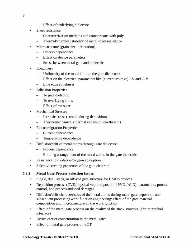
8
Technology Transfer #03024377A-TR International SEMATECH
– Effect of underlying dielectric
• Sheet resistance
– Characterization methods and comparisons with poly
– Thermal/chemical stability of metal sheet resistance
• Microstructure (grain size, orientation) – Process dependence
– Effect on device parameters
– Stress between metal gate and dielectric
• Roughness
– Uniformity of the metal film on the gate dielectrics
– Effect on the electrical parameters like (current-voltage) I-V and C-V
– Line edge roughness
• Adhesion Properties – To gate dielectric
– To overlaying films
– Effect of moisture
• Mechanical Stresses
– Intrinsic stress (created during deposition)
– Thermomechanical (thermal expansion coefficient)
• Electromigration Properties – Current dependence
– Temperature dependence
• Diffusion/drift of metal atoms through gate dielectric
– Process dependence
– Bonding arrangement of the metal atoms in the gate dielectric
• Resistance to oxidation/oxygen absorption
• Selective etching properties of the gate electrode
5.3.2 Metal Gate Process Selection Issues
• Single, dual, stack, or alloyed gate structure for CMOS devices
• Deposition process (CVD/physical vapor deposition [PVD]/ALD), parameters, process control, and process-induced damages
• Diffusion/drift characteristics of the metal atoms during metal gate deposition and subsequent processingWork function engineering: effect of the gate material composition and microstructure on the work function
• Effect of the metal gate process on the quality of the stack structure (abrupt/gradual interface)
• Active carrier concentration in the metal gates
• Effect of metal gate process on EOT

9
International SEMATECH Technology Transfer #03024377A-TR
5.3.3 Stability Related Needs and Questions for Metal Gates • Thermal stability with gate dielectrics
– Expected to be stable under source/drain dopant activation
– Minimal interface reactions between metal and the gate dielectrics
• Mechanical Stability – Effect of thermal cycling on interface stability
• Electrical stability
– Charge trapping
– NBTI lifetime
– Defect generation rates (bulk and at the interfacial)
– Mobile ions
• Plasma damage associated with metal-gate deposition
5.4 Reliability Metrics
The following measures should be considered when characterizing the reliability of metal gate devices:
• Thermal stability (% shift) of metal gate work function and critical device parameters (Ioff, Idrive, Vt, etc.)
• Electrical properties (% shift): leakage, threshold voltage, mobility, effective dielectric constant of the gate stack, barrier heights for charge injection, etc.
• Fixed charge (< 1E10/cm2) in the gate dielectric due to metal gate process
• Mobile ions (< 1E10 ions/cm2) in the gate dielectrics due to metal gate process
• Defect density (<0.1 defects/cm2) characterization: across wafer, wafer-to- wafer, and lot-to-lot.
• I-V and C-V variations (area dependence)
• Impact of backend processing (plasma damage/antenna data)
• Impact of metal gate on the conduction model (voltage dependence and activation energy)
• Electrical stability (% shift for key device parameters under temperature and bias stress); as a reference condition: 125°C/1.4 × VCC
5.5 Effect of Metal Gates on the Reliability Physics
• Time-dependent dielectric breakdown (TDDB) model (voltage/field/temperature dependence)
• VBD and TDDB distributions (slopes/area scaling)
• SILC measurement
• Trap generation rate
• Polarity dependence and device dependence (N and P)
• Hot carrier effects
• Plasma damage/antenna effects
10
Technology Transfer #03024377A-TR International SEMATECH
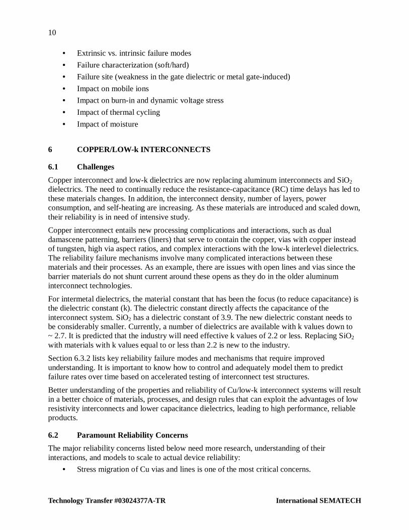
• Extrinsic vs. intrinsic failure modes
• Failure characterization (soft/hard)
• Failure site (weakness in the gate dielectric or metal gate-induced)
• Impact on mobile ions
• Impact on burn-in and dynamic voltage stress
• Impact of thermal cycling
• Impact of moisture
6 COPPER/LOW-k INTERCONNECTS
6.1 Challenges
Copper interconnect and low-k dielectrics are now replacing aluminum interconnects and SiO2 dielectrics. The need to continually reduce the resistance-capacitance (RC) time delays has led to these materials changes. In addition, the interconnect density, number of layers, power consumption, and self-heating are increasing. As these materials are introduced and scaled down, their reliability is in need of intensive study.
Copper interconnect entails new processing complications and interactions, such as dual damascene patterning, barriers (liners) that serve to contain the copper, vias with copper instead of tungsten, high via aspect ratios, and complex interactions with the low-k interlevel dielectrics. The reliability failure mechanisms involve many complicated interactions between these materials and their processes. As an example, there are issues with open lines and vias since the barrier materials do not shunt current around these opens as they do in the older aluminum interconnect technologies.
For intermetal dielectrics, the material constant that has been the focus (to reduce capacitance) is the dielectric constant (k). The dielectric constant directly affects the capacitance of the interconnect system. SiO2 has a dielectric constant of 3.9. The new dielectric constant needs to be considerably smaller. Currently, a number of dielectrics are available with k values down to ~ 2.7. It is predicted that the industry will need effective k values of 2.2 or less. Replacing SiO2 with materials with k values equal to or less than 2.2 is new to the industry.
Section 6.3.2 lists key reliability failure modes and mechanisms that require improved understanding. It is important to know how to control and adequately model them to predict failure rates over time based on accelerated testing of interconnect test structures.
Better understanding of the properties and reliability of Cu/low-k interconnect systems will result in a better choice of materials, processes, and design rules that can exploit the advantages of low resistivity interconnects and lower capacitance dielectrics, leading to high performance, reliable products.
6.2 Paramount Reliability Concerns
The major reliability concerns listed below need more research, understanding of their interactions, and models to scale to actual device reliability:
• Stress migration of Cu vias and lines is one of the most critical concerns.

11
International SEMATECH Technology Transfer #03024377A-TR
• Cu via and line electromigration performance and the impact of surrounding materials, processing, and stress. Early life and long-term failure mechanisms require study.
• Thermal-mechanical stability of the interfaces between metals, barriers, and interlevel dielectrics and the resulting line-to-line leakage.
• TDDB of the Cu/low-k system (line-to-line leakage and breakdown).
• Reliability impact of lower thermal conductivity of low-k dielectric.
• Reliability issues due to the porous nature of the low-k dielectrics and moisture ingress (weight gain and dimensional shifts).
• Reliability impact of the lower mechanical strength in the Cu/low-k system, including the impact of packaging.
6.3 Research Needs and Questions
6.3.1 Material Properties
6.3.1.1 Copper • Cu resistivity, what controls it: surface scattering, phonon interactions, microstructure,
barrier materials, impurities, processing?
• Cu resistivity increases as line sizes are reduced: why?
• Cu interaction with barrier materials and low-k dielectrics (all at minimum feature dimensions)
– Adhesion
– Young’s modulus
– Thermal expansion coefficients
– Thermal conductivity
• Barrier material properties (liner and top layer cap)
• Cu alloys: impacts on resistivity and reliability
• Resistivity changes over time under storage conditions (e.g., microstructure/impurity redistribution effects, stress relaxation)
6.3.1.2 Low-k Dielectrics • Pore size
– Measurement methods (which ones are best?)
– Mean and distribution: need to know if “killer pores” (i.e., pores that are a significant fraction of minimum line width) are likely
– Open vs. closed pores
– Uniformity
– Thickness
– Composition
• Chemical-mechanical polishing (CMP) limits
– The industry may not use soft/weak low-k materials at upper levels of metal. Instead, hard conventional CVD layers may be used, making this effect less of a concern.
12
Technology Transfer #03024377A-TR International SEMATECH
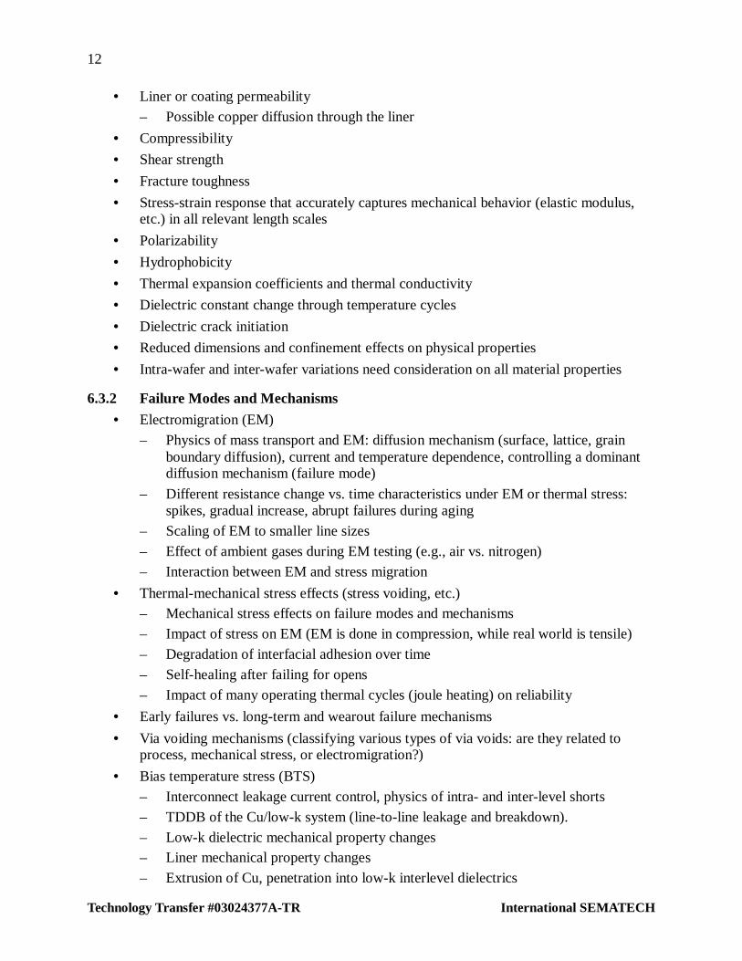
• Liner or coating permeability
– Possible copper diffusion through the liner
• Compressibility
• Shear strength
• Fracture toughness
• Stress-strain response that accurately captures mechanical behavior (elastic modulus, etc.) in all relevant length scales
• Polarizability
• Hydrophobicity
• Thermal expansion coefficients and thermal conductivity
• Dielectric constant change through temperature cycles
• Dielectric crack initiation
• Reduced dimensions and confinement effects on physical properties
• Intra-wafer and inter-wafer variations need consideration on all material properties
6.3.2 Failure Modes and Mechanisms
• Electromigration (EM)
– Physics of mass transport and EM: diffusion mechanism (surface, lattice, grain boundary diffusion), current and temperature dependence, controlling a dominant diffusion mechanism (failure mode)
– Different resistance change vs. time characteristics under EM or thermal stress: spikes, gradual increase, abrupt failures during aging
– Scaling of EM to smaller line sizes
– Effect of ambient gases during EM testing (e.g., air vs. nitrogen)
– Interaction between EM and stress migration
• Thermal-mechanical stress effects (stress voiding, etc.) – Mechanical stress effects on failure modes and mechanisms
– Impact of stress on EM (EM is done in compression, while real world is tensile)
– Degradation of interfacial adhesion over time
– Self-healing after failing for opens
– Impact of many operating thermal cycles (joule heating) on reliability
• Early failures vs. long-term and wearout failure mechanisms
• Via voiding mechanisms (classifying various types of via voids: are they related to process, mechanical stress, or electromigration?)
• Bias temperature stress (BTS)
– Interconnect leakage current control, physics of intra- and inter-level shorts
– TDDB of the Cu/low-k system (line-to-line leakage and breakdown).
– Low-k dielectric mechanical property changes – Liner mechanical property changes
– Extrusion of Cu, penetration into low-k interlevel dielectrics

13
International SEMATECH Technology Transfer #03024377A-TR
– CMP, processing impacts
• Moisture and ambient gas effects on interconnect reliability, including moisture in interlevel dielectrics
• Impact of die top passivation and/or additional damage protection die topcoat
• Cu corrosion, stress-corrosion cracking
• Low-k dielectric deformation from EM stress
• Low-k dielectric voiding
• Interaction with other residual process chemicals
• Shear stress failure from temperature cycling stress (delamination of one of many interfaces; there are more in a dual damascene architecture than a subtractive non-copper system)
• Liner failure (work is beginning on “pore sealing”—methods to seal pores before liner deposition—this could reduce penetration of liner process precursors into pores and/or improve integrity/reliability of the liner on porous sidewalls)
• Package assembly
– Bond pad integrity
– Solder bumping and wire bonding reliability to Cu/low-k
– Die edge seal integrity
– Stress induced by packaging; impact on stress-induced voiding and delamination
– Brittle fracture of low-k in die core
6.3.3 Physical Model and Model Parameters • Models to predict product reliability from accelerated reliability testing and a method
for extrapolating results to different designs, e.g., different number of vias and line lengths, different operating conditions?
• Feature size dependence of failure mechanisms (e.g., Blech-length effect, linewidth dependence)
• Models or simulations to predict the interconnect stress states
• General integrated predictive model for copper/low-k system through thermal and mechanical stresses
6.3.4 Test Structures and Methods
• Structures that simulate typical device structures (sizes, spaces, vias, surrounding metals, stress states, etc.)
• Impact of joule heating, temperatures, stress states, and stress gradients
• Line sizes, spaces, and via dependence on reliability
• Adapt test structures into product-like architectures and test at use conditions – Large product-like test chip
• Structures to measure barrier defects at time zero and over time
• Electromigration from 200°C to 400°C (different mechanical stress state than operating conditions)

14
Technology Transfer #03024377A-TR International SEMATECH
– Constant current
– Pulsed current (pulses near dielectric thermal time constant)
– Effect on Blech length
– Linewidths and spaces
– Short and long straight lines with/without vias
– Long lines with various turns (90° and 45°)
• Bias/humidity testing: characterize impact of voltage and moisture ingress on reliability
• Low-k dielectric TDDB
• Measure effects of temperature cycling
• Measure effects of power cycling
• Wire bonding variation effects with differing bond pad structures
• Measure effects of temperature cycling with humidity testing
• Potential moisture ingress effects on die edge seal structures
6.3.5 Stability of Parameters as Function of Stress and Time
• Resistivity of vias and lines
• Barrier and liner integrity
• Capacitance over time and temperature
• Current leakage over time and temperature
• Mechanical strength over time and temperature
6.4 Reliability Metrics
Circuit failure rates over time and lifetime before wearout must be predicted, given parameters such as currents in vias and lines, temperatures, line size and spacing, and interline voltages. Some of the useful reliability metrics are as follows:
• Failures in time (FITS)/m length/cm2; active wiring only, excluding global levels
• FITS as a function of the number of vias
• Jmax (A/cm2): wire at 125°C or other temperatures
• Imax (ma): via at 125°C or other temperatures
• Stability of line and via chain resistance over thermal stress and time
• Measurement of barrier/liner quality (defect density)
• Water weight gain vs. pore size and distribution
7 SILICON ON INSULATOR (SOI)
7.1 Challenges
The use of silicon on insulator (SOI) as a substrate material for ICs offers the possibility of significantly increased performance using traditional transistor formats, as well as major increases in performance using radically new transistor structures. These opportunities come at the expense of both the cost of changing the substrate and yield and reliability concerns over the

15
International SEMATECH Technology Transfer #03024377A-TR
use of new materials and structures, as well as new device operating modes. These concerns arise from structural features, such as defects in the buried oxide and contamination of the surface silicon during the SOI fabrication process. They also occur because of possible reliability issues related to new device operating modes, such as the effects of fully depleted device operation on leakage currents and thermal problems due to confinement by the buried oxide.
Reliability of SOI devices operating in a non-fully depleted mode with thick buried oxides (~ 40–400 nm) have been not demonstrated new failure modes on bulk devices. Reliability of SOI devices operating in the fully depleted mode, as well as new transistor structures allowed by SOI, have not received adequate reliability evaluation.
Power density (W/cm2) has increased >30X in the last two decades with no sign of decreasing in the foreseeable future, unless new technologies such as SOI are introduced, Even with the introduction of new technologies like SOI, many devices will likely increase performance rather than minimize power dissipation. Not only must high current levels be delivered to the die, but the resulting thermal load through both active and passive methods must be dissipated. Thermal interface materials must maintain their properties for the life of the product. Intra-die thermal profiles must be mapped and simulated to ensure thermal and reliability solutions comprehend worst-case situations. Mechanical stresses introduced by the increasing mass of passive solutions or the complexity of active solutions must be evaluated over the product’s lifetime. Since SOI may not be as efficient at heat dissipation through the die because of the buried oxide—even with the lower power devices offered by SOI—intra-die thermal non-uniformity or “hot spots” may increase.
The following tables list reliability-related research needs and specific reliability metrics suggested for SOI device evaluation.
7.2 Paramount Reliability Concerns
A reliability-based understanding is needed of the overall thermal, mechanical, and electrical interaction of SOI with other process modules. Areas of particular concern include the following:
• Carrier mobility: Clearly carrier mobility (circuit switching speed) must be maintained and stable vs. mechanical stress (packaging, metal/interlevel dielectric stack, strained Si such as SiGe epitaxial mismatch) while parasitic capacitance is reduced.
• SOI substrate defects interaction with high-k dielectric or its interfacial layer(s): Because of multiple methods to produce SOI substrate with different defect density values, the potential for interaction with really thin interfacial layers preceding high-k dielectric deposition may prove to be a challenging set of issues.
• Metal gates: SOI defects could well influence properties for subsequent deposited layers, such as the interfacial layer before high-k dielectric and similarly for metal gates with the proper work function.
7.3 Research Needs and Questions
7.3.1 Material Properties • Thermal conductivity vs. temperature and vs. (Si28) isotopic purity
• Anisotropy and carrier scattering
• Mobility (p and n) vs. thickness, temperature, mechanical stress (piezo effects, coupling of stress and mobility or resistance), etc.

16
Technology Transfer #03024377A-TR International SEMATECH
• Measure mobility variance with temperature, electric field, impurity gradient, frequency
• Quantify mobility changes as modulated by interfacial surface or edge roughness and back interface
• Quantify electron or hole mobility changes if isotopically pure Si were used (Si28)
• Learn if Brillioun zones discontinuities are an issue that would change mobile carrier electrical properties (analogous to birefringence)
• Establish whether SOI is inherently compatible with new gate dielectrics based on Hf or Zr oxides, silicates, or nitrides
• Measure electrical and mechanical effects to SOI from intermediate layers relevant to strained Si
• Quantify effects of epitaxial or amorphous carbon upon SOI
7.3.2 Configuration and Organization
• Understand relative merits and demerits of fully vs. partially depleted SOI
• Understand implications of using well ties or not
• Establish whether low-k dielectrics are relevant or not for performance and reliability
• Establish perturbation to SOI if gate material is something other than traditional poly Si or a silicide. Establish effects of metal gates (possibly different gate composition for n-channel and p-channel MOS transistors upon SOI
• Measure SOI flat band shifts and interface state density and position
• Measure and minimize parasitic capacitance, especially Miller capacitance
• Develop a new set of ESD protection algorithms and circuits as conventional (bulk) ESD designs cannot be copied over to SOI (much SOI-specific design is necessary)
• Measure SOI effects on bipolar device characterization
• Characterize advanced device structures such as FINFET1, double gates, etc
• Develop solutions to issues of contacts to thin Si film in fully depleted SOI
• Characterize impact of raised junctions
7.3.3 Failure Modes and Mechanisms
• Defect feature size dependence upon failure rates; e.g., determine range and size of killer defects. Use St. Venant’s Principle to estimate mechanical stress decay range and magnitude.
• Apply percolation theory for defects in SOI.
• Perform physical and electrical characterization of concentration vs. depth and laterally.
• Simulate overall thermal, mechanical, and electrical performance of the die/package/board subsystem containing SOI.
1 A non-planar double gated transistor that has been proposed by researchers and is now being developed within the industry. It derives its name from the fact that the device is built with a fin that sits on top of the silicon with the gate wrapping around both sides.

17
International SEMATECH Technology Transfer #03024377A-TR
7.3.4 Statistical Models • Determine Weibull beta or lognormal sigma (time dispersion) as appropriate to each
failure mechanism.
• Determine if Arrhenius modeling of temperature dependence for a single, dominant mechanism is appropriate or if methods to deconvolute the observations need to be developed.
• Determine statistical scatter in device parameters (i.e., Vt, etc.), especially for fully depleted (FD) SOI.
7.3.5 Test Structures • Design new test structures (for rapid fault isolation) specific to SOI to comprehend
floating body (FB), tied body (TB), and FD issues, especially FB potential stability and TB resistance.
• Test structures to study the impact of mechanical stress/strain and poor thermal impedance, NOT confounded with other issues and specifically sensitive to a single failure mechanism or defect.
7.3.6 Stability of Parameters as a Function of Stress and Time
• Stress can mean mechanical, electrical, or environmental (bake, cycling, humidity, etc.)
7.4 Reliability Metrics
• Hysteresis during each clock cycle, delay time equality for positive and negative switching, carrier mobility vs. bulk Si, mobile carrier scattering, impurity gradient effects (“drain engineering”): same issues as bulk Si, so issue will be to maintain parity to bulk while reaping SOI speed benefits
8 NOVEL DEVICES
8.1 Challenges
The ITRS defines what is needed to sustain the historic doubling of performance with each new microelectronics technology generation; 1.4X of this performance increasing has come from transistor scaling. (The other 1.4X has come from design improvements.)
For the last 20 years the planar CMOS transistor has dominated the industry. As the difficulties (e.g., increasing power) of scaling grow with each new generation, the ability to stay with the planar CMOS transistor is being questioned. There will likely be a succession from planar CMOS to non-planar CMOS (e.g., raised source/drain) to dual-gate CMOS (e.g., FINFET) to novel devices (e.g., C nanotubes, molecular electronics). The ITRS predicts the something beyond non-planar CMOS could be needed as early as 2007. Low power applications, which are much more sensitive to increased power consumption with each new generation, are likely to be the first adopters of new materials and new device structures.
The move from planar CMOS to non-planar CMOS to double gate CMOS should involve the same historic transistor failure modes (oxide breakdown and hot carrier effects). The changes in materials that will occur in these devices, especially the introduction of alternative high-k gate insulators, will likely have a more profound impact on reliability than the changes in device

18
Technology Transfer #03024377A-TR International SEMATECH
geometry. However, changing geometry may change an existing failure mode or introduce a new failure mode (Murphy’s Law).
On the other hand, the move to novel devices should have profound reliability impacts. These devices involve new materials and new methods of operating and will surely have new failure modes. General guidance can be provided about what to look for in these new devices. Material integrity and catastrophic/gradual changes in electrical properties are generic areas of reliability concern.
Novel devices are in their infancy and demonstrating practical devices is still in the distance. Not much reliability work is likely to have been done. If history is a guide, work on the reliability of these novel devices will be late and sub-critical. Bringing reliability issues upstream in the development process will result in a better assessment of the readiness of these technologies for volume production.
8.2 Paramount Reliability Concerns • Non-planar CMOS could change transistor failure modes.
• New failure modes could appear in novel devices with new materials, new geometries, and new methods of operation.
• Robust reliability engineering capabilities need to be developed for novel devices including test structures, test techniques, and acceleration methods.
8.3 Research Needs and Questions
• Double-gated CMOS; FINFET – TDDB measurement and modeling
– Hot carrier effects and NBTI measurement and modeling
• Carbon nanotubes – Material properties
• Conductivity
• Doping
• Mobility
– Electromigration, voiding
– Interconnect to tube reliability
– Degradation of electrical performance
• Molecular electronics
– Material properties
• Conductivity
• Processing
– Interconnect reliability
– Wearout in switching mechanisms

19
International SEMATECH Technology Transfer #03024377A-TR
9 MICROSYSTEMS
9.1 Challenges
SOC seeks to add value by integrating different technologies onto a single chip. Initially, the SOC focus is on “homogeneous” integration of several microelectronics technologies such as logic, DRAM, and nonvolatile on a single chip. Moving forward, the ITRS had identified the need for “heterogeneous” integration of microelectronics with non-microelectronics technologies such as optoelectronics and MEMS often referred to as microsystems or smart microsystems.
From a reliability perspective, microsystems require consideration of a wider range of failure modes than microelectronics alone. Each of the technologies incorporated into the microsystem has different failure modes. Furthermore, failure modes can be associated with the interaction of the technologies when integrated on a single chip that would not be present if each technology were manufactured on a separate chip. The integration of two or more technologies often requires different processing than if each technology were separately fabricated on a separate chip.
A major market for microsystems will be sensors, especially chemical and biological applications. This presents an additional reliability challenge. In microelectronics, the active devices are sealed first with the final layer of passivation on the chip and later with the package. Chemical and biological sensors often have to be open to the environment to allow the species to be measured to come in physical contact with the sensor. Being exposed to the environment could expand the set of possible failure modes for microsystems. Sensitive coatings are used in chemical and biological microsensors. The integrity and degradation of these coatings pose a serious reliability issue.
Semiconductor optoelectronics is concerned with generating, producing, and/or manipulating photons of light. The light emitting junctions can form defects during operation that limit output. The transmission and reflection in optical channels and at surfaces can also degrade. Optical interconnect may be needed when the parasitic RC of Cu/low-k interconnect technology is no longer acceptable.
MEMS involve mechanical devices. Associated with mechanical devices are failure modes such as wear and cracking. Another problem in MEMS is stiction, a sticking together of adjacent surfaces that results from the high surface-to-volume ratios in the miniaturized mechanical elements (e.g., beams) in MEMs. The reliability of MEMs devices is sensitive to surface properties and environmental factors such as humidity.
Building in reliability and reliability qualification of microsystems is obviously much more challenging that microelectronics alone. The new failure modes need to be identified and modeled. Methods of characterizing and accelerating these failure modes also need to be developed. Given the time and effort required to develop the knowledge base and tools for IC reliability, considerable effort will need to be expended to develop highly reliable microsystems.
9.2 Paramount Reliability Concerns
Non-microelectronics technologies (e.g., MEMS, sensors) could also introduce new failure modes, which would need to be identified and modeled.
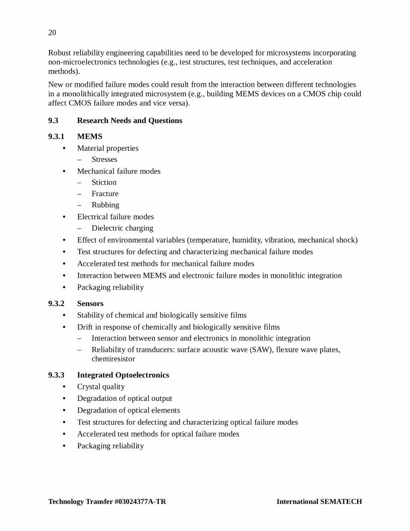
20
Technology Transfer #03024377A-TR International SEMATECH
Robust reliability engineering capabilities need to be developed for microsystems incorporating non-microelectronics technologies (e.g., test structures, test techniques, and acceleration methods).
New or modified failure modes could result from the interaction between different technologies in a monolithically integrated microsystem (e.g., building MEMS devices on a CMOS chip could affect CMOS failure modes and vice versa).
9.3 Research Needs and Questions
9.3.1 MEMS
• Material properties – Stresses
• Mechanical failure modes – Stiction
– Fracture
– Rubbing
• Electrical failure modes
– Dielectric charging
• Effect of environmental variables (temperature, humidity, vibration, mechanical shock)
• Test structures for defecting and characterizing mechanical failure modes
• Accelerated test methods for mechanical failure modes
• Interaction between MEMS and electronic failure modes in monolithic integration
• Packaging reliability
9.3.2 Sensors • Stability of chemical and biologically sensitive films
• Drift in response of chemically and biologically sensitive films – Interaction between sensor and electronics in monolithic integration
– Reliability of transducers: surface acoustic wave (SAW), flexure wave plates, chemiresistor
9.3.3 Integrated Optoelectronics • Crystal quality
• Degradation of optical output
• Degradation of optical elements
• Test structures for defecting and characterizing optical failure modes
• Accelerated test methods for optical failure modes
• Packaging reliability

21
International SEMATECH Technology Transfer #03024377A-TR
10 FLASH MEMORIES
10.1 Challenges
Flash memory is a quickly growing and widely accepted memory technology in today’s marketplace. In addition, embedded Flash is emerging as a key memory technology, especially for SOC. However, the reliability challenge for Flash increases because of the poorly scalable program/erase voltage associated with ever-shrinking CMOS technology. Fast program and erase operations require high voltage and high current stress on the dielectric either at the edge with hot carrier injection or tunneling through the channel. Stress-induced leakage current through tunnel oxide impacts data retention. Actually, reliability is the only factor limiting tunnel oxide and interpoly dielectric scaling. This process enlarges the mismatch between the aggressively scaling gate dielectric of CMOS and non-scalable cell dielectrics. This mismatch also aggravates the difficulty of embedding Flash devices within other types of semiconductor processes, resulting in a greater reliability challenge.
10.2 Paramount Reliability Concerns
Data retention capability is an important reliability concern for Flash memory technology. To meet the 10-year reliability requirement, the charge loss rate must be less than a couple electrons per hour during normal operations. The quality of the surrounding cell dielectrics becomes extremely important to guarantee retention reliability. Random data retention failure bits are caused by latent defects in the dielectrics, which are induced during either process or program/erase cycling. Voltage acceleration and temperature dependency of these weak bits are different from the intrinsic population; reliability lifetime characterization and detection/screening pose a major challenge, especially in automotive applications, which require a single digital ppm level.
• Data retention of weak bits as a function of temperature and voltage
• Detection and screening of weak bits
10.3 Reliability Requirements and Research Needs
Long charge retention, a large number of endurance cycles, and disturb immunity are the most important parameters to continuously shrink Flash memory technology cells. First, 10-year non-volatility is commonly required for a Flash cell. To assure 10 years of data storage, retention capability of Flash memories has to be checked by accelerated stresses, usually high electric fields and hostile environments at high temperature. Therefore, a comprehensive model is needed to estimate the acceleration factor accurately. Nowadays, lack of a good data retention model hinders the precise prediction of Flash memory lifetime under normal operation, especially to satisfy of a statistically meaningful distribution based on millions of cells in a memory array.
10.3.1 Data Retention • Charge gain/loss mechanism: different mechanisms in different temperature ranges
complicate interpretation of acceleration stresses
• Annealing (recovery): At high temperatures, annealing of program/erase (P/E)-induced damage can occur. The annealing temperature is dependent on technology and process.
• Acceleration factor: A matrix of temperature, voltage, and numbers of P/E cycling are inputs from which acceleration factors can be calculated. A model needs to comprehend all factors.

22
Technology Transfer #03024377A-TR International SEMATECH
• Damage induced by P/E results in a wide distribution of leakage current and only a very limited number of cells (at ppm level or less) show some charge loss during voltage-accelerated retention tests. Beside the knowledge of the acceleration factors, a statistical model is required to extrapolate from the small number of tested devices to millions of shipped devices.
• Data retention at high and low temperature (HTDR and LTDR)
• Data retention performance is critical at both high and low temperatures, which show different failure mechanisms. The robustness of the device depends how the technology has developed. Good understanding and characterization of data retention are critical.
10.3.2 Endurance • Market requirements vary from 1,000 to more than 1,000,000 cycles, and the memory
card requirement is usually high.
10.3.3 Multi-Level Cell in a Single Flash Transistor
• To define many threshold levels, either the margins between each level are reduced or the threshold window is increased. In the first case, reading errors could arise, in the second the electric field in the cell dielectrics during storage is increased with negative impact on data retention.
• Circuit complexity: For the same reason, to design a sensing circuit for multi-bit per cell is more complicated and challenging than for single-bit per cell.
10.3.4 Design
• Design for testability and manufacturability is needed to optimize the wafer fabrication process.
• Increased sensing accuracy helps reduce the threshold window and thus the electric field in the cell dielectrics during storage.
• The soft error rate (SER) at low voltage operation is as critical as other types of memory devices (i.e., SRAM and DRAM).
10.3.5 Testing • Screen weaker cells by using optimized program and erase methods based on statistical
analysis in each given design style.
• Skew voltage levels to detect outliers.
• Use thermal and electrical stress conditions to identify abnormal cells.
10.4 Reliability Metrics
The most important metrics for measuring and reporting reliability for Flash memories are:
• Program/erase capability (# cycles allowed)
• Data retention (ppm in product lifetime)

23
International SEMATECH Technology Transfer #03024377A-TR
11 SOFT ERRORS
11.1 Challenges
The term “soft error” generally relates to a random error or corruption of data in an electronic system that occurs because of an external influence such as an energetic particle, electrical noise, electromagnetic interference (EMI), etc. The error affects only the data; the device itself is not physically damaged or prone to new errors anymore than before the event. While the effects of electrical noise and EMI are generally addressed in a satisfactory manner by sound design and shielding practices, energetic particles pose distinct challenges and design considerations.
For several decades now, the occurrence of energetic particle-related soft errors has been known and characterized as a key reliability failure mode. It was first observed in space and later in terrestrial systems. Neutrons originating from cosmic rays and ionizing particles from radioactive decay have been implicated. The first observations in electronic components were made in dynamic random access memories (DRAMs). As technology scaling made the basic circuits in the electronic components more susceptible, soft error were observed in static random access memories (SRAMs), and logic circuits in microprocessors, and related components.
The relentless demand for increased performance and the integration of increased levels of functionality results in aggressive technology scaling trends. A key feature of this technology scaling is the dimensional reduction for density, reduced capacitance for performance, and reduced voltage for improved performance/power ratios. The inevitable result of this scaling is less electrical charge in the data storage nodes, which in turn results in less node critical charge. Node critical charge is defined as a threshold for injected charge beyond which an error in the stored data or circuit voltage level will occur and propagate to other circuit locations.
The overall trend suggests that when the effects of the reduction in critical charge, scaling of the active area, materials, and circuit layout and architecture changes are comprehended, the SER per bit will decrease for DRAMs while be approximately flat for SRAMs and logic latch components. Meanwhile, the bit count in memories is increasing rapidly, as is the added functionality integrated in logic components. Furthermore, there is a strong tendency to use multi-processor implementations to increase performance. The result is that without actively addressing the issue, the system SER is expected to increase significantly in new products.
A lot of work has been done over many years to reduce the impact of soft errors. Error detection and correction schemes are commonly used for memories. Progress in material and manufacturing controls has resulted in the availability of low alpha emission materials, although emissions continue to need to be reduced. System-level redundancy is often used for fail-safe systems at a significant increase in cost and complexity. Time and space redundancy at the latch level is also used for high radiation environments, but carry significant area and performance penalties. The main challenge remains on developing effective schemes to protect random logic circuit sections while achieving performance targets and staying cost-effective for the commercial market.
11.2 Paramount Reliability Concerns
Technology scaling will result in increased failure rates from soft errors. This is primarily due to the increased functionality being integrated into each chip and the increasingly frequent implementation of multi-processor and complex multi-chip systems.
24
Technology Transfer #03024377A-TR International SEMATECH
Research in the areas below is considered critical for successful “management “ of soft error-related concerns in advanced technologies:
• Error detection and correction schemes for random logic circuits that minimize the penalty to performance and area
• Improved latch designs to reduce SER in a cost-effective manner (minimize the performance, area, and power costs)
• Improved error derating methods in random logic circuits
• System methods to mitigate the impact of soft errors
• SER implications of novel technologies (like FD SOI) and novel devices (like FINFET or TriGate)
11.3 Research Needs and Questions
11.3.1 Memories • Improved error detection and correction schemes in multi-chip memory systems
• Improved error detection and correction schemes in memories (within chip) for both single and multi-bit error events
• Improved methods to estimate error derating for memory components and systems and their relation to applications
• Simple and cost-effective methods for accelerated testing in memories
• System-level, non accelerated SER measurement capabilities and methods for memories
11.3.2 Logic Components and Systems
• Error detection and correction schemes for random logic circuits that minimize the penalty to performance and area
• Improved methods to estimate the true error rate of logic components both silent and detected, including logic derating methods
• Cost-effective, within-chip redundancy schemes for multi-core microprocessor implementations
• Cost-effective system-level error detection, correction and recovery schemes for logic components and systems
• Simple and cost-effective methods for accelerated testing in microprocessors and other logic circuits
• System-level, non-accelerated SER measurement capabilities and methods for microprocessor components
• Field SER metrology methods
• Test structures for alpha and neutron sensitivity measurements in logic latches
11.3.3 Materials
• Cost-effective and simple to use alpha emission rate metrology capability < 0.001 alpha/cm2*hr
• Manufacturing and process control of wafer and package fabrication materials with alpha emission rates significantly lower than 0.001 alpha/cm2*hr

25
International SEMATECH Technology Transfer #03024377A-TR
11.3.4 Models and Simulation • Accurate waveforms for charge injection during alpha and neutron strikes
• Accurate simulation capability for both alpha and neutron strikes in memory cells, logic latches, and combinatorial circuitry
• Improved models that relate latch layout and electrical parameters to SER sensitivity
• Models and estimates of the reduction in SER for SOI in both partially and fully depleted implementations
• Improved methods to correlate accelerated test results to expected field error rates
11.4 Reliability Metrics
• Failure rates expressed in FITs, where 1 FIT = 1E-9 failures/(device-hr). Alternatively the median time between failures (MTBF) can be used.
• Soft Error Failure Rates due to alpha particles emitted from Radioactive decay
– Total alpha emission rate for manufacturing materials in α/(cm2-hr)
• The energy spectrum of a sheet of 228Th between 3–8 MeV is often used for simulation and as a comparative reference
– SER/memory bit in FIT/(bit)
– SER/latch or logic state storage element in random logic in FIT/latch
– SER/circuit for combinational logic feeding data into a latch in FIT/circuit
– SER/chip in FIT (Sum of the three components above weighted by their corresponding counts and de-rating factors)
12 ELECTROSTATIC DISCHARGE PROTECTION
12.1 Challenges
ESD protection ranges from designing protection circuits/devices against human handling (human body model [HBM]), machine discharges (machine model [MM]) and charged chips being charged and discharged (charge device model [CDM]). In all ESD protection networks, the ESD device must protect the active circuits from these events. With the aggressive scaling of CMOS, SOI, and BICMOS technologies, the constraints (area, capacitive loading and leakage currents to list a few) on the ESD protection circuits are making them more difficult to design and meet the Joint Electron Device Engineering Council (JEDEC), electrical overstress (EOS)/ESD, and other industry recognized specification requirements.
As the scaling of CMOS-based devices continues, the frequency of the I/O circuits and other circuits that need to communicate off-chip to other chips is increasing. Ideally, the ESD device area needs to scale at a similar rate as the rest of the circuits and the capacitive loading of the ESD device to be reduced proportionally to the increase in the I/O circuit speeds. As the technology scales, the ESD current that ESD devices must be able to handle without damage occurring remains constant; this drives the need for innovation in improving the effectiveness of ESD devices in each new technology generation to allow the ESD device area and capacitive loading to be scaled/reduced.

26
Technology Transfer #03024377A-TR International SEMATECH
12.2 Paramount Reliability Concerns • Effects of scaling
• Potential for latent damage
• Compatible protection techniques for radio frequency (RF) applications
12.3 Research Needs and Questions
• Device simulation related needs and questions
– ESD device simulators with improved convergence with breakdown and temperature models turned on
• Device design-related needs and questions
– ESD devices with low on-resistance along with low capacitive loading (<100 fF), RF applications
– Low turn-on voltage ESD devices (<0.5 V)
– Low leakage (<1 pA) ESD devices for low power applications
– Correlation of ESD design elements to final product and understanding of performance gaps
• Compact model-related needs and questions
– High current ESD device models compatible with running on industry standard spice simulators with self-heating and breakdown models incorporated into the compact equivalent circuit
– RF quality ESD device models for RF applications (diodes, silicided and non-silicided MOSFETS)
– Oxide breakdown models accurate for HBM and CDM types of pulses
• Testing related needs and questions:
– 2000+ pin HBM testers: is it possible to still achieve waveforms within the defined specifications?
– Transmission line pulse (TLP) testers capable of testing 1000+ pins for debugging
– HBM ESD testers capable of full functional testing in addition to HBM zapping
– Wafer-level HBM and TLP testing of full product chips, 100–1000+ pads tested and correlation of test methods
– Very fast TLP investigation and correlation to CDM testing
– Development of non-destructive test methods for measuring ESD robustness
• Latent damage needs and questions
– ESD pulse effects on oxide lifetimes, MOSFET-based ESD protection devices
– ESD pulse effects on hot electron shift, MOSFET-based ESD protection devices
– ESD pulse effects on electromigration, metal interconnect structures
12.4 Reliability Metrics
• Failure voltage per unit width (V/µm)
• Failure current (It2) per unit width (mA/µm)
27
International SEMATECH Technology Transfer #03024377A-TR
13 LATCHUP
13.1 Challenges
Latchup can be classified into two generalized categories: internal and external. Internal latchup occurs when circuits are not connected to I/O pads, whereas external latchup occurs when circuits or injection sources are connected to pads. With the aggressive scaling of CMOS, SOI, and BICMOS technologies, the ground rules are being reduced to allow greater numbers of transistors in a given die size. The reduction in the ground rules leads to smaller N+(PWELL)/P+(NWELL) spacing, which in turn increases the parasitic NPN and PNP betas, lowering the trigger currents/voltages and the holding voltage. With the introduction of triple well bulk CMOS technologies, new NPNs and PNPs are formed that will need to be considered beyond the classical NPNs and PNPs formed in a dual well bulk CMOS technology.
13.2 Paramount Reliability Concerns
• Effects of scaling and increasing resistivity of wells
• Potential for latent damage
13.3 Research Needs and Questions
• Device simulation-related needs and questions
– Latchup device simulators with improved convergence with breakdown and temperature models turned on
• Device design-related needs and questions:
– Effective guarding designs in I/O circuits
– Reduced NWELL and PWELL sheet resistances for improvements in trigger currents while minimizing junction area capacitances and maintaining low junction area leakages for low power applications
– Increased shallow trench isolation (STI) depths for reduction in parasitic betas
• Compact model-related needs and questions
– RF quality parasitic NPN and PNP models for accurate transient latchup simulations
– Improved extraction tools/algorithms to extract only the most important parasitic latchup structures while ignoring the less important latchup structures for run time improvements
– Accurate latchup models after triggering occurs, holding/sustaining regime of parasitic latchup structure
• Testing-related needs and questions
– 2000+ pin latchup testers: is it possible to still achieve waveforms within the defined specifications?
– Transient latchup testers, 1000+ pins
– Latchup testers capable of full functional testing in addition to applying latchup trigger pulses
– Wafer-level latchup testing of full product chips, 100–1000+ pads contacted and tested
28
Technology Transfer #03024377A-TR International SEMATECH
– Development of non-destructive test methods
• Latent damage needs and questions
– Non-destructive latchup, potential effects on hot electron, oxide lifetime, and electromigration
14 IMPACT OF SCALING ON PACKAGING
14.1 Challenges
Moore’s Law, stating that the number of transistors doubles every 18–24 months, has proven remarkably accurate over the past 30 years and all indications are it will remain accurate as markets continue to demand maximum performance and minimum cost. The performance demands that continue to drive this scaling at the silicon level result in profound challenges to the packaging development and reliability technologist.
Using microprocessors as a benchmark, the impacts of Moore’s Law can be identified. Die size has grown approximately 7% annually since the early 1970s. Over the same period, microprocessor transistor count increased from 5000 to 42,000,000. Frequency doubles every 2 years, and power has increased at an exponential rate. These trends have had significant impact on packaging technology. As the number of transistors and frequency increases, the required number of interconnects between the die and package has grown to accommodate increased signal count as well as power and ground to support the increased demand for power. Silicon-to-package interconnects have increased more than sixfold over the past 5 years. This has required first level interconnect technology to transition from peripheral wire bonding to area array bumping. However, scaling demands are currently driving bump size and pitch to the limits of current technologies. As bump size decreases, the bump becomes less compliant because of the geometry, making it more susceptible to thermal- and mechanical-driven failure modes such as fracture. Bump scaling can also drive new materials, which in turn may introduce a new set of reliability challenges as a result of basic material properties, interfacial concerns, etc.
The increase in first level interconnects has also resulted in a corresponding increase in both the number and complexity of intra-package signal and power routing to connect the die to the package terminals. Using the past 5 years of microprocessors as a model, the number of package vias has increased ~ 25X. Organic substrates using lithographic techniques have replaced the once familiar lead frame and plastic or ceramic package. The resulting reduced interconnect geometries are susceptible to increased metal migration and electromigration risks. Interfacial delamination is a continuing concern as the number of interfaces within the package increases with complexity. Increasing frequency demands contribute to the move to organic packages and copper interconnects to reduce dielectric constant and resistance. Power demands continue to increase with increases in transistor count.
Power density (W/cm2) has increased > 30X since the advent of the microprocessor and shows no sign of decreasing. Not only must high current levels be delivered to the die, but the resulting thermal load through both active and passive methods must be dissipated. The reliability of these package thermal solutions needs to be understood. Thermal interface materials must maintain their properties for the life of the product. Intra-die thermal profiles must be mapped and simulated to ensure thermal and reliability solutions comprehend worst-case situations. The mechanical stresses introduced by the increasing mass of passive solutions or the complexity of active solutions must be evaluated over the product’s lifetime. Silicon technologies also need to

29
International SEMATECH Technology Transfer #03024377A-TR
consider thermal issues. For example, SOI may not be as efficient at heat dissipation through the die, resulting in increased intra-die thermal non-uniformity or “hot spots.”
The move to low-k dielectrics at the silicon level has impacts at both the package and board levels. To accommodate the reduced thermal and mechanical robustness of these dielectrics, package designers have employed materials with lower CTEs. While this reduces the die-to-package expansion mismatch, it increases the package-to-board mismatch. This is further aggravated by reduced solder ball sizes, resulting in solder joint reliability risks at the motherboard level.
Although not directly related to scaling, the move to “lead (Pb) free” packaging increases the risks introduced by scaling. Higher processing and mounting temperatures increase thermal stresses. Ball and bump metallurgy changes will require new reliability modeling. For example, increased Sn content coupled with decreasing package pitches requires an increased understanding of the factors contributing to “Sn whiskers.”
The reliability challenges posed by specialized market segments also need to be recognized. These include, but are not limited to, impacts of extended temperature ranges in segments such as automotive/military/aerospace and the need for reliability test methods and metrics for optical-related materials and components.
The market’s demand for maximum performance and minimum cost has also increased the complexity involved in evaluating reliability. Single products no longer can serve all applications with significant reliability and performance margins. An increasing number of products is being developed for specific market segments. Performance and reliability are tailored for the segment’s needs. Leading-edge performance may require shorter product lifetime targets. Since packages can be market segment specific, material choices and reliability evaluations will differ depending on the segment, even when the same die is used. Thus, reliability evaluations can no longer be based on standard tests and readouts. A failure mechanism approach must be employed, identifying failures and evaluating their impact based on the specific requirements of the segment. A much improved understanding of materials properties and failure mechanisms and models is required. To increase the rate of acceptance of model-based reliability, industry accepted guidelines for reliability modeling are needed. Decisions derived from standards-based tests and readouts risks building in excessive reliability at the expense of performance and cost or failure due to mismatched tests and segment application.
14.2 Paramount Reliability Concerns
A reliability-based understanding is needed of the overall thermal, mechanical, and electrical interaction of the die/package/board sub-system. Areas of particular concern include the following:
• Bump metallurgy: ability to withstand thermal and mechanical stresses while providing sufficient current carrying capability
• Solder joints: fracture at first and second level interconnects
• Electromigration: package traces, vias, and bumps
• Temperature coefficient mismatch: impact of increasing CTE mismatch between low-k silicon and organic packages

30
Technology Transfer #03024377A-TR International SEMATECH
14.3 Research Needs and Questions
14.3.1 Materials Properties
• Thermal interface materials
• Bump metallurgy to withstand thermal and mechanical stresses while providing sufficient current carrying capability
• Pb-free solders
• Impact of higher processing temperatures
• Organic substrates with embedded passives
• Alternative flame retardant molding compounds
• First-level interconnect to Cu and surfaces containing low-k dielectrics
14.3.2 Failure Modes and Mechanisms • Package-level electromigration: package traces, vias, and bumps
• Metal migration; traces, vias, bumps
• Solder joint fracture at first and second level interconnects
• Lead-free solders: creep, fracture, whisker growth, etc.
• Interfacial delamination of organic and metallic interfaces
14.3.3 Physical Models and Model Parameters • Feature size dependence of failure mechanisms (e.g., pitch and bump diameter impact
on metal migration)
• Modeling of multi-chip and stacked die/stacked package architectures
• Physical and electrical characterization of thinned die
• Simulation of overall thermal, mechanical, and electrical performance of the die/package/board sub-system
• Thin film cracking and adhesion properties
• Shock and vibration stress modeling
• Intermittent first and second level connections
• Impact of fragile, porous low/ultra low-k interlevel dielectrics on package integrity
• Impact of increasing temperature coefficient mismatch between low-k silicon and organic packages
• Impact of increasing package fragility driven by low-k and organic materials
14.3.4 Test Structures
• Thermal and interconnect test die incorporating – Design rules enabling rapid fault isolation
– Thin film cracking sensors and connectivity daisy chains for bumps and vias
– Localized die heaters
• Improved tools for rapid fault isolation such as
– Design software tools to rapidly identify connectivity paths

31
International SEMATECH Technology Transfer #03024377A-TR
– Automated time domain reflectometry (TDR) with correlation to design tools
• Reliability Metrics
– Figures of merit for
• Solder joint reliability (defined by four-point bend, bump shear, bump pull, etc.)
• Low-k dielectric thin film cracking and delamination
• Bake resistance of underlying C4 bump metallurgy
• Thermal degradation
15 DESIGN FOR RELIABILITY (DFR)
15.1 Challenges
Reliability is a key product attribute equivalent to product performance that must be integrated very early into the product design and development cycle. The expertise required to drive reliability engineering closer to product design requires the use of advanced engineering computer-aided design (CAD) tools. Although modeling and simulation support have been used to a limited degree, support is generally sporadic or inconsistent and does not provide the focus required for an effective reliability engineering that leads to design for reliability (DFR).
Many electronic design automation (EDA) companies have made remarkable progress in developing primary design tools, but the tool capabilities have not been addressed proactively. Commercial reliability design tools are lacking necessary DFR capabilities that are important today and are becoming increasingly necessary as very deep sub-micron (VDSM) technology is approached. The application of CAD tools and the development of standard tools for DFR are needed to design reliability into the product at the design phase.
One of the major challenges is to raise awareness of the need to optimize reliability and circuit performance. Typically, designers give lower priority to reliability checks, shifting this responsibility to the process engineer. Consequently, individual companies may not provide enough funding to develop internal tool solutions or purchase tools from EDA suppliers to solve reliability design issues. Decoupled design and reliability disciplines are expected to gradually become concurrent and interactive as reliability margins diminish with advanced technology.
Another challenge is the lack of commonality in methodologies and models being used in DFR tools. Individual companies have developed tools that are company-specific, typically using a single style of design. EDA companies do not have consensus for DFR requirements and specifications that drive toward flexible tools, which might appeal to a broad customer base. Therefore, industry-wide communication is important; EDA companies need to focus on generic and common tool issues rather than on proprietary design rules or methods. The EDA industry needs to develop solutions to meet semiconductor industry-wide needs.
The ultimate challenge for DFR will be for the capabilities to be mature enough that device (product) qualifications will be reduced and/or eliminated based on materials (process) qualifications and DFR reliability simulation techniques.
32
Technology Transfer #03024377A-TR International SEMATECH
15.2 Paramount Needs
The most critical need is to raise awareness of the need for DFR within the design community. It is imperative that the design process comprehend reliability and manufacturability needs as well as product performance.
• Simulation tools for concurrent optimization of circuit performance and reliability
• DFR tools that are accurate and efficient in dealing with large and complex circuits
• Methodology that could identify more realistic toggle/switching activity of nodes for large and complex circuits
• Tools that simulate failure mechanisms. Priority should be given to – Electromigration
– Thermal-mechanical stress
– Process-induced charging/antenna effects
15.3 Research Needs and Questions
15.3.1 CAD Tool and Data Interface
CAD tool/data interface items are the features, data, and hooks needed in existing design tools; are very important to enable correct-by-design (CBD):
• Application program interface (API) functions to support reliability simulations
• Rule-based, constraint-driven router
• RC extraction tool
– Inadequate for reliability needs
– Need to include details like fuse
• Electrical rule check (ERC) capabilities for reliability
• Support for mixed-level simulation tools
• Realistic toggle/switching activity
• Automatic transistor sizing tools for hot carrier injection (HCI) reliability and verification
• Tools to support both worst-case and typical-case analysis with flexible reliability models
15.3.2 Reliability Point CAD Solutions – Standalone Tools • Hot carrier injection (HCI)
– Path analysis, timing analysis tool with capability to simulate aged path
– Coupling effects: effects of parasitic coupling (both capacitive and inductive) taken into account
• Circuit topology
• Rise/fall time
• Electromigration (EM): Extensive electromigration checking is needed in circuit design and synthesis as well as place and route. Design tools need to be able to recognize high frequency nodes, place desired loads together, and do tight routing.
33
International SEMATECH Technology Transfer #03024377A-TR
– Signal integrity
– Power CBD
– EM signal CBD
– Hierarchical verification
– EM DRC
– Data pruning
– Stress modeling, comprehending increases in interconnect complexity and power density vs. decreasing thermal conductivity and mechanical strength
• Interface with router tools for design construction at first pass
• Placement of metal fro improved thermal dissipation
• Electrostatic discharge (ESD): Robust ESD design tools are required that comprehend antenna effects and know when and where to insert diodes automatically.
• Soft error rate (SER) (see Section 11) – Failure rate
– Sensitive structure tool
16 IMPACT OF DEFECT SCREENING ON DEVICE RELIABILITY
Defect screening is essential to achieve the levels of device quality and reliability demanded in today’s and tomorrow’s applications. Screening at the earliest feasible point in the process is fundamental to achieving good reliability as well as high yields. Fatal defects associated with yield loss have been linked with latent defects that affect device reliability. Therefore, yields can be one of the earliest predictors of subsequent device reliability. Even wafers/lots with high yields can contain devices with latent defects. The screening of these latent defects is essential to achieve excellent reliability.
16.1 Challenges
Scaling has been the lifeblood of the semiconductor industry for the last four decades, while the current ITRS suggests Moore’s Law will continue to be a target for the next two decades. While semiconductor history to date has been evolutionary, the pace will quicken substantially with new materials, new configurations, and new architectures. Thus, new kinds of defects will complement the current roster. The semiconductor industry will need new tools to detect and prevent traditional, though smaller, defects and new kinds of defects. An important element of the change in semiconductor device structure is the rapidly increasing number of metallization levels, having changed from ~ 3 just a decade ago to ~ 8 now, perhaps with three-dimensional structures in the future. Clearly, visual inspection cannot detect defects in opaque, multilayer structures; consequently, other imaging or electrical methods must be used to infer that defects exist and to deduce their site among millions or billions of transistors. Whereas the transistor count is increasing exponentially (smaller dimensions and bigger chips), the number of connections to the “outside” world is not increasing as rapidly. Rent’s Rule is an empirical relationship between the number of connections and number of gates, roughly a power law with an exponent of 0.6. Hence “access” is becoming elusive (unless IEEE 1149.1, Boundary Scan, is used). While current navigation tools (with schematic, logic diagram, mask layout) can help find defect sites, these tools will become overwhelmed with data. A method is needed for

34
Technology Transfer #03024377A-TR International SEMATECH
comprehending mask hierarchy or flatness (number of layers, concatenation, union, interference, etc.).
The huge complexity of semiconductor devices with hundreds of millions of transistors is not limited to semiconductor devices; “packages” or higher level integration structures have substantial complexity as well (many layers, vias, connections, bumps, contacts, material interfaces, etc.). These increased levels of integration are effectively including mechanisms previously associated with board and system reliability in product reliability.
Computing-intensive applications also are trending towards higher current/peak power/peak temperature. At the same time, electrical performance requirements are driving towards the use of materials that are less thermally and mechanically robust. These high junction temperature applications using less robust materials significantly limit the effectiveness of traditional burn-in screens.
Currently electrical defect screening (greatly superior to visual) is done in the context of functional and parametric testing at wafer sort and final test and during the fabrication process. An example of the latter would be a measurement of sheet resistance, metal stack via resistance, propagation delay signature, junction depth, Idsat, etc., which is found to be statistically different than normal process variation. If the aberration were irreparable (e.g., critical dimension in lithography is repairable if a new resist is applied and exposed), then scrapping some portion of the material or sort of compensation scheme using future process steps must be considered. Defects are commonly found using parametric values to sort marginal or failing material into bins (sometimes “soft bins” for additional discrimination, e.g., opens, shorts, pin leakage, quiescent power supply current). Often devices are subjected to a matrix of clock speeds and power supply voltage values (i.e., a “schmoo”) to find defective material.
Another commonly used technique is to impose a stress at higher than normal operating temperature or voltage (e.g., dynamic voltage screen [DVS]) to “kill” defective devices while minimally damaging ordinary material with normal process variation. Burn-in at high temperature and often elevated voltage is the safety net. While DVS is an effective technique, finding the proper combination of voltage and time is a non-trivial exercise and sometimes other issues can take control (e.g., thermal management may preclude effective DVS)
Other techniques rely upon looking at the distribution of values. For example, one might statistically test data to see if it is Gaussian, measure the sigma, and detect extraneous modes.
Statistical analysis could be used as a guide to take appropriate actions to compensate. While maps are often used to look for patterns from which defect sources can be inferred, statistical correlation techniques are rarely used. Memory devices are inherently amenable to highly effective node test coverage (finding stuck or leaky nodes), but random logic is far more difficult, though boundary scan techniques work well at a cost. Good ways to measure and improve test coverage are lacking.
While Iddq (quiescent power supply current) was an important diagnostic when static power (clock stopped) was small, the devices currently fabricated with thin gate oxides vulnerable to quantum mechanical tunneling currents, have such great quiescent currents that defects cannot be seen (a classic difference of large numbers problem). Ironically, efforts in high dielectric constant gate materials may produce the very thin effective oxide thickness values needed to improve performance while still using a thick gate dielectric such that static current draw is reduced by several orders of magnitude. These high-k materials, however, may introduce new classes of defects (non-stoichiometry, vacancies, fixed charge, mobile charge, etc.). Diagnostic
35
International SEMATECH Technology Transfer #03024377A-TR
test structures (or test chips) are needed that can unambiguously identify the kind of defect present, its density, and its site.
16.2 Paramount Reliability Concerns
A reliability-based understanding of each kind of defect (in the Si, the metal/dielectric stack, in package interconnect, etc.) and an indicator that permits defect detection and quarantine are needed. Areas of particular concern include the following:
• Safe dynamic voltage stress: While some techniques exist (measure mean and standard deviation for “killing” defect-free samples), they are not widely applied (cut and try or history takes precedence) and raise many unanswered questions. For example, to what degree is the safe voltage influenced by duration, temperature, frequency, and other factors?
• Screen for “Opens” especially within each layer: DVS has been effective for finding shorts, traditionally the most common defects, but multiplayer metallization stacks (currently 7–10 layers deep) suffer to a greater degree from opens than shorts; therefore, DVS and high temperature operating life (HTOL) are much less effective. Some FA tools exist for opens, but using these tools is destructive (decapsulation) and they have generally poor spatial resolution. Opens within layers are the current problem as aspect ratio is substantially different than previously (narrow critical dimension [CD] and thick layers, so sidewall area >> top or bottom).
• Detection of resistive and capacitively coupled interconnect, matching electrical screen to physical defect: One element is the unambiguous test structures described above, but another would be to characterize the “link” between a given defect and some set of perturbed electrical properties, a signature. Naturally, an electrical response might vary with defect size, type, and location.
• Unambiguous Test Structures: Functional devices with millions over even billions of gates are ill suited for easy interpretation of the relationship between the existence of defects (density, site, size, etc.) and perturbed electrical properties. However, suitable test structures can be tailored to be sensitive to a specific defect or design issue; e.g., electromigration or HCI jeopardy is commonly addressed with suitable test structures now, but many other issues need similar attention (stress migration).
16.3 Research Needs and Questions
16.3.1 Defect Properties • Density and location
• Percolation theory made practical
• In-process detection for each unique defect type during manufacturing rather that at end of line
• Electrical characterization much preferred to visual or mechanical as more easily recorded, sorted, classified, correlated to other data
• Optical recognition (e.g., fingerprint, face print) capability
16.3.2 Failure Modes and Mechanisms
• Electromigration (extrinsic defect induce)
36
Technology Transfer #03024377A-TR International SEMATECH
• Gate dielectric breakdown (extrinsic defectivity)
• Opens or partial (resistive) contacts or vias
• Opens/crack propagation
• Opens/bump defect
• Opens/package substrate via barrel plating failure
• Ball opens/shorts/coplanarity warpage at reflow temperature
• Interfacial delamination of organic and metallic interfaces
• Impact of fragile low/ultra low-k interlevel dielectric on package integrity
• Metal line voids and extrusions
• Thermal interface material degradation/pumping
• Opens/shorts as a function of temperature and handling damage (introducing defects)
16.3.3 Physical Models and Model Parameters
• Defect size dependence of failure mechanisms; e.g., killer size vs. critical dimension
• Modeling and simulation to know what electrical (possible image signatures) signatures are connected with each kind of defect
• Physical and electrical characterization of each defect type (an atlas?)
• Simulation and characterization of overall thermal, mechanical, and electrical performance of the die/package/board subsystem
16.3.4 Statistical Models
• Simulations to predict the effect of defect size distribution or location upon yield and reliability
16.3.5 Latent Defect Screens (Detection Methods)
• Burn-in (HTOL)
• Bake
• Accelerated voltage, especially stepwise to failure (DVS)
• Temperature cycle, thermal shock, or power cycling
• Sequential step stress
16.3.6 Test Structures
• Thermal test die to measure thermal impedance
• Improved tools for rapid fault isolation
• Unambiguous identification of defect type
16.3.7 Stability of Parameters as a Function of Stress and Time
• Establish market segment use requirements
• Early life (warranty) requirement

37
International SEMATECH Technology Transfer #03024377A-TR
• Wearout requirements for frequency degradation, operating life, and temperature/power cycle life
• Improved tools for rapid fault isolation
16.4 Reliability Metrics
• Development of a latent or reliability defect density statistic R0 which might include – Fraction (ppm) escaping as a function of overvoltage
– Fraction (ppm) not in the central population
– FITs in HTOL or user environment
• Time dispersion index for the failures (lognormal sigma or Weibull beta)
• Infant mortality defects actually screened to 6 σ


International SEMATECH Technology Transfer 2706 Montopolis Drive
Austin, TX 78741
http://www.sematech.org e-mail: [email protected]