
CQM1H/CJ1M/CJ1G Replacement Guide · 2020-03-21 · CQM1H/CJ1M/CJ1G Replacement Guide From CQM1H to...
52
CQM1H/CJ1M/CJ1G Replacement Guide From CQM1H to CJ2M From CJ1M/CJ1G to CJ2M
Transcript of CQM1H/CJ1M/CJ1G Replacement Guide · 2020-03-21 · CQM1H/CJ1M/CJ1G Replacement Guide From CQM1H to...

CQM1H/CJ1M/CJ1G Replacement Guide
From CQM1H to CJ2MFrom CJ1M/CJ1G to CJ2M

About this documentThis document provides the reference information for replacing CQM1H/CJ1M/CJ1G PLCsystems with CJ2M series PLC.This document does not include precautions and reminders; please read and understand theimportant precautions and reminders described on the manuals of PLCs (both of PLC used inthe existing system and PLC you will use to replace the existing PLC) before attempting to startoperation.

Man.No. Manual
W472 CJ2 CPU Unit Hardware USER'S MANUAL
W473 CJ2 CPU Unit Software USER'S MANUAL
W486 CJ2M Pulse I/O Module USER'S MANUAL
W393 CJ Series OPERATION MANUAL
W441 CJ series CJ1M CPU Units with Ethernet Functions OPERATION MANUAL
W395 CJ series Built-in I/O CJ1M CPU Units OPERATION MANUAL
W394 CS/CJ/NSJ PROGRAMMING MANUAL
W474 CS/CJ/NSJ Series INSTRUCTIONS REFERENCE MANUAL
W342 CS/CJ/CP/NSJ Series Communications Commands REFERENCE MANUAL
W345 CS/CJ Series Analog I/O Units AD/DA/MAD42 OPERATION MANUAL
W368 CS/CJ Series Analog I/0 Units OPERATION MANUAL
W466 CJ Series Universal Input Units OPERATION MANUAL
W396 CJ Series Temperature Control Units OPERATION MANUAL
W401 High-speed Counter Units OPERATION MANUAL
W465 EtherNet/IP Units OPERATION MANUAL
W420 CS and CJ Series Ethernet Units OPERATION MANUAL Construction of Networks
W343 CS/CJ Series Ethernet Units OPERATION MANUAL
W421 CS/CJ Series Ethernet Units OPERATION MANUAL Construction of Applications
Z174 CS/CJ Series ID SENSOR UNITS OPERATION MANUAL
W397 CJ Series Position Control Units CJ1W-NC□□3 OPERATION MANUAL
W477 CJ Series Position Control Units CJ1W-NC□□4 OPERATION MANUAL
W336 CS/CJ Series Serial Communications Boards Serial Communications Units OPERATION MANUAL
W426 CS/CJ Series Position Control Units CS1W-NC□□1/CJ1WNC□□1-MA OPERATION MANUAL
W435 CS/CJ series Motion Control Unit CS1W/CJ1W-MCH71OPERATION MANUAL
W467 Controller Link Support Boards for PCI Bus INSTALLATION GUIDE
W309 Controller Link Units OPERATION MANUAL
V237 SPU-Console Ver.2.1 OPERATION MANUAL
W406 CS/CJ Series Loop Control Boards/Process-control CPU Units /Loop-control CPU Units OPERATION MANUAL
W407CS/CJ Series Loop Control Boards/Process-control CPU Units /Loop-control CPU Units FUNCTION BLOCKREFERENCE MANUAL
W364 CQM1H Series Programmable Controllers Inner Boards PROGRAMMING MANUAL
W365 CQM1H-SCB41 SERIAL COMMUNICATIONS BOARD OPERATION MANUAL
W238 CQM1H/CQM1 Series Dedicated I/O Units OPERATION MANUAL
W364 CQM1H Series Programmable Controllers Inner Boards PROGRAMMING MANUAL
W463 CX-One FA Integrated Tool Package SETUP MANUAL
W446 CX-Programmer OPERATION MANUAL
W447 CX-Programmer OPERATION MANUAL:Function Blocks/Structured Text
W469 CX-Programmer OPERATION MANUAL SFC Programming
W366 CX-Simulator OPERATION MANUAL
W464 CX-Integrator OPERATION MANUAL
W433 CX-Position OPERATION MANUAL
W436 CX-Motion-NCF OPERATION MANUAL
W448 CX-Motion-MCH OPERATION MANUAL
Related Manuals
Read and Understand this DocumentPlease read and understand this document before using the product. Please consult your OMRON representative if you have any questions or comments.
Warranty and Limitations of Liability
WARRANTY
OMRON's exclusive warranty is that the products are free from defects in materials and workmanship for a period of one year (or other period if specified) from date of sale by OMRON.
OMRON MAKES NO WARRANTY OR REPRESENTATION, EXPRESS OR IMPLIED, REGARDING NON-INFRINGEMENT, MERCHANTABILITY, OR FITNESS FOR PARTICULAR PURPOSE OF THE PRODUCTS. ANY BUYER OR USER ACKNOWLEDGES THAT THE BUYER OR USER ALONE HAS DETERMINED THAT THE PRODUCTS WILL SUITABLY MEET THE REQUIREMENTS OF THEIR INTENDED USE. OMRON DISCLAIMS ALL OTHER WARRANTIES, EXPRESS OR IMPLIED.
LIMITATIONS OF LIABILITY
OMRON SHALL NOT BE RESPONSIBLE FOR SPECIAL, INDIRECT, OR CONSEQUENTIAL DAMAGES, LOSS OF PROFITS OR COMMERCIAL LOSS IN ANY WAY CONNECTED WITH THE PRODUCTS, WHETHER SUCH CLAIM IS BASED ON CONTRACT, WARRANTY, NEGLIGENCE, OR STRICT LIABILITY.
In no event shall the responsibility of OMRON for any act exceed the individual price of the product on which liability is asserted.
IN NO EVENT SHALL OMRON BE RESPONSIBLE FOR WARRANTY, REPAIR, OR OTHER CLAIMS REGARDING THE PRODUCTS UNLESS OMRON'S ANALYSIS CONFIRMS THAT THE PRODUCTS WERE PROPERLY HANDLED, STORED, INSTALLED, AND MAINTAINED AND NOT SUBJECT TO CONTAMINATION, ABUSE, MISUSE, OR INAPPROPRIATE MODIFICATION OR REPAIR.

Disclaimers
CHANGE IN SPECIFICATIONS
Product specifications and accessories may be changed at any time based on improvements and other reasons.
It is our practice to change model numbers when published ratings or features are changed, or when significant construction changes are made. However, some specifications of the products may be changed without any notice. When in doubt, special model numbers may be assigned to fix or establish key specifications for your application on your request. Please consult with your OMRON representative at any time to confirm actual specifications of purchased products.
DIMENSIONS AND WEIGHTS
Dimensions and weights are nominal and are not to be used for manufacturing purposes, even when tolerances are shown.
PERFORMANCE DATA
Performance data given in this manual is provided as a guide for the user in determining suitability and does not constitute a warranty. It may represent the result of OMRON's test conditions, and the users must correlate it to actual application requirements. Actual performance is subject to the OMRON Warranty and Limitations of Liability.
ERRORS AND OMISSIONS
The information in this manual has been carefully checked and is believed to be accurate; however, no responsibility is assumed for clerical, typographical, or proofreading errors, or omissions.
Application Considerations
SUITABILITY FOR USE
OMRON shall not be responsible for conformity with any standards, codes, or regulations that apply to the combination of products in the customer's application or use of the products.
At the customer's request, OMRON will provide applicable third party certification documents identifying ratings and limitations of use that apply to the products. This information by itself is not sufficient for a complete determination of the suitability of the products in combination with the end product, machine, system, or other application or use.
The following are some examples of applications for which particular attention must be given. This is not intended to be an exhaustive list of all possible uses of the products, nor is it intended to imply that the uses listed may be suitable for the products:
• Outdoor use, uses involving potential chemical contamination or electrical interference, or conditions or uses not described in this manual.
• Nuclear energy control systems, combustion systems, railroad systems, aviation systems, medical equipment, amusement machines, vehicles, safety equipment, and installations subject to separate industry or government regulations.
• Systems, machines, and equipment that could present a risk to life or property.
Please know and observe all prohibitions of use applicable to the products.
NEVER USE THE PRODUCTS FOR AN APPLICATION INVOLVING SERIOUS RISK TO LIFE OR PROPERTY WITHOUT ENSURING THAT THE SYSTEM AS A WHOLE HAS BEEN DESIGNED TO ADDRESS THE RISKS, AND THAT THE OMRON PRODUCTS ARE PROPERLY RATED AND INSTALLED FOR THE INTENDED USE WITHIN THE OVERALL EQUIPMENT OR SYSTEM.
PROGRAMMABLE PRODUCTS
OMRON shall not be responsible for the user's programming of a programmable product, or any consequence thereof.

Table of Contents 1. Performance specifications 1.1 CQM1H/CJ2M specifications comparison 1.2 CJ1M/CJ2M specifications comparison 1.3 CJ1G/CJ2M specifications comparison 2. System Configurations 2.1 CQM1H/CJ2M system comfiguration comparison 2.2 CJ1M/CJ1G/CJ2M system comfiguration comparison 3. Memory area 3.1 CQM1H/CJ2M memory area comparison 3.2 CJ1M/CJ1G/CJ2M memory area comparison 4. I/O Area Allocation 5. Instructions 5.1 High-speed counter/pulse output instruction 5.2 I/O instructions 5.3 Model conversion instructions 6. Example of converting ladder program by CX-Programmer Appendix A-1 Instruction operations A-2 Condition flag operations
1

1. Performance specifications 1.1 CQM1H/CJ2M specifications comparison
The table below lists the major difference in specifications of the CQM1H series and CJ2M series. Item CQM1H-CPU11/21/51/61 CJ2M-CPU**
Number of I/O points CPU11/21: 256 points CPU51/61: 512 points
2,560 points
Program capacity Note1. CPU11/21: 3.2k words CPU51: 7.2k words CPU61: 15.2k words
Note1. CPU*1: 5k step CPU*2: 10k step CPU*3: 20k step CPU*4: 30k step CPU*5: 60k step 32k words Data memory CPU11/21: 3.k words (DM)
CPU51: 6k words (DM) CPU61: 12k words (DM+EM)
EM CPU*1 to *3: 1 bank (32k) CPU*4 to *5: 4 banks (32k x 4)
Built-in I/O In:16 points Built-in CPU funciton will be available by adding the CJ2M-MD211/CJ2M-MD212. Up to two units can be mounted. In: 10 points/Out: 6 points (when one unit is used). In: 20 points/Out: 12 points (when two units are used). Attention: It is possible to use the unit with
the CPU Unit of unit version 2.0 or later. Length of instructions Note1.
1-4 words/one instruction Note1. 1-30 steps/one instruction
LD instruction 0.375us 0.04us Execution time of instruction
MOV instruction 17.7us 0.12us
Overhead processing time 0.70ms CPU3*: 270us CPU1*: 160us
Maximum Number of Connectable Units
16 units 40 units
Maximum Number of Expansion Racks
1 3
Clock function Available. Optional memory cassette is necessary.
Equipped as a standard function.
Dimensions (CPU Unit) 110(H)x187(W)x107(D) CPU1*: 90(H)x31(W)x75(D) CPU3*: 90(H)x62(W)x75(D)
Programming software SSS,CPT,CX-P CX-P Programming
ice for personal computer
dev
< Peripheral port connection > Connection with PC requires cables:CS1W-CN*** or CS1W-CN114 + CQM1-CIF**. < RS232 C port connection > Connection with PC requires a cable: XW2Z-***S (-V).
< Peripheral (USB) port > A direct connection can be made between the USB port of the personal computer and the PLC using the commercially-available USB cable. < Serial (RS232C) port connection > Use the serial cable (XW2Z-200S-CV/500S-CV) to connect the PC and serial port on the CPU Unit. (The CPU3* does not have the RS232C port on it. Mount the RS232C option board (CP1W-CIF01) and connect the cable with the unit).
Programming device connection
Programming Console
Available C200H-PRO27 CQM1-PRO01
Not available
Note1. One word of CQM1H corresponds to one step of CJ2M. For instance, replacement model of CQM1H-CPU51 (7.2k word) is CJ2M-CPU*2 (10k step), since the program capacity of 7.2k step or larger is required for replacement. Note that the number of steps for an instruction might be different in CQM1H and CJ2M.
< Example > TIM instruction: CQM1H: 2 word/CJ2M: 3 step
2

1.2 CJ1M/CJ2M specifications comparison
The table below lists the major difference in specifications of the CJ1M series and CJ2M series. Item CJ1M-CPU** CJ2M-CPU**
Number of I/O points CPU*1: 160 points CPU*2: 320 points CPU*3: 640 points
2,560 points
Program capacity CPU*1: 5k step CPU*2: 10k step CPU*3: 20k step
CPU*1: 5k step CPU*2: 10k step CPU*3: 20k step CPU*4: 30k step CPU*5: 60k step 32k words Data memory 32k words
EM CPU*1 to *3: 1 bank (32k) CPU*4 to *5: 4 banks (32k x 4)
Built-in I/O CJ2*: In:10 points/Out:6 points
Built-in CPU funciton will be available by mounting CJ2M-MD211/CJ2M-MD212. Up to two units can be mounted. In:10 points/Out:6 points (when one unit is used) In:20 points/Out:12 points (when two units are used) Attention: It is possible to use the unit with
the CPU Unit of unit version 2.0 or later. Length of instructions 1-7 steps/one instruction 1-30 steps/one instruction
LD instruction 0.10us 0.04us Execution time of instruction
MOV instruction 0.30us 0.12us
Overhead processing time CPU*1: 0.7ms CPU*2/*3: 0.5ms
CPU3*: 270us CPU1*: 160us
Maximum Number of Connectable Units
CPU*1/CPU*2: 10 units CPU*3: 20 units
40 units
Maximum Number of Expansion Racks
CPU*1/CPU*2: No expansion CPU*3: 1
3
Clock function Equipped as a standard function Equipped as a standard function Dimensions (CPU Unit) CPU*1: 90(H)x31(W)x65(D)
CPU*2: 90(H)x49(W)x65(D) CPU*1: 90(H)x31(W)x75(D)
CPU*3: 90(H)x62(W)x75(D) Programming software CX-P CX-P
Programming ice for
personal computer
dev< Peripheral port connection > Connection with PC requires cables:CS1W-CN*** or CS1W-CN118 + XW2Z-***S-** < RS232C port connection > Connection with PC requires cables:XW2Z-***S-CV or XW2Z-***S(-V).
< Peripheral (USB) port > A direct connection can be made between the USB port of the personal computer and the PLC using the commercially-available USB cable < Serial (RS232C) port connection > Use the serial cable (XW2Z-200S-CV/500S-CV) to connect the PC and serial port on the CPU Unit. (The CPU3* does not have the RS232C port on it. Mount the RS232C option board (CP1W-CIF01) and connect the cable with the unit)
Programming device connection
Programming Console
Available C200H-PRO27 CQM1-PRO01
Not supported
3

1.3 CJ1G/CJ2M specifications comparison The table below lists the major difference in specifications of the CJ1G and CJ2M series.
Item CJ1G-CPU4*H/CPU4* CJ2M-CPU**
Number of I/O points CPU42H/43H: 960 points CPU44/45/44H/45H: 1280 points
2,560 points
Program capacity CPU42H: 10k step CPU43H: 20k step CPU44/44H: 30k step CPU45/45H: 60k step
CPU*1: 5k step CPU*2: 10k step CPU*3: 20k step CPU*4: 30k step CPU*5: 60k step 32k words Data memory 32k words
EM CPU*1 to *3: 1 bank (32k) CPU*4 to *5: 4 banks (32k x 4)
Built-in I/O - Built-in CPU funciton will be available by adding the CJ2M-MD211/CJ2M-MD212. Up to two units can be mounted. In:10 points/Out:6 points (when one unit is used) In:20 points/Out:12 points (when two units are used) Attention: It is possible to use the unit with
the CPU Unit of unit version 2.0 or later. Length of instructions 1-7 steps/one instruction 1-30 steps/one instruction
LD instruction CPU4*H: 0.04us CPU4*: 0.08us
0.04us Execution time of instruction MOV instruction CPU4*H: 0.20us
CPU4*: 0.29us 0.12us
Overhead processing time CPU4*H : 0.3ms CPU4*: 0.5ms
CPU3*: 270us CPU1*: 160us
Maximum Number of Connectable Units
40 units 40 units
Maximum Number of Expansion Racks
3 3
Clock function Equipped as a standard function Equipped as a standard function Dimensions (CPU Unit) 90(H)x62(W)x65(D) CPU1*: 90(H)x31(W)x75(D)
CPU3*: 90(H)x62(W)x75(D) Programming software CX-P CX-P
Programming ice for
personal computer
dev
< Peripheral port connection > Connection with PC requires cables:CS1W-CN*** or CS1W-CN118 + XW2Z-***S-** < RS232C port connection > Connection with PC requires cables:XW2Z-***S-CV or XW2Z-***S(-V)
< Peripheral (USB) port > A direct connection can be made between the USB port of the personal computerand the PLC using the commercially-available USB cable < Serial (RS232C) port connection > Use the serial cable (XW2Z-200S-CV/500S-CV) to connect the PC and serial port on the CPU Unit. (The CPU3* does not have the RS232C port on it. Mount the RS232C option board (CP1W-CIF01) and connect the cable with the unit)
Programming device connection
Programming Console
Available C200H-PRO27 CQM1-PRO01
Not supported.
4

2. System Configurations
2.1 CQM1H/CJ2M system comfiguration comparison This section describes the CJ2M series units which can be used instead of the CQM1H series units. Functions which have been supported by the CQM1H series unit can be generally supported by the CJ2M series unit. However, there are some differences in usage, connecting method with external devices, and input/output specifications. Please check if the CJ series unit can be used instead of the CQM1H units, by referring to the user's manuals of both series. ♦Power Supply Unit
Unit CQM1H CJ2M CQM1-PA203 CJ1W-PA202 AC Power
Supply Unit 100 to 240 VAC, 50/60Hz Output capacity 18W, No DC
service power supply
100 to 240 VAC, 50/60Hz Output capacity 14W, No DC service
power supply CQM1-PA206 CJ1W-PA205R AC Power
Supply Unit 100 to 240 VAC, 50/60Hz Output capacity 30W
DC service power supply 24VDC/0.5A
100 to 240 VAC, 50/60Hz Output capacity 25W
No DC service power supply, with RUN output
CQM1-PD026 CJ1W-PD025 DC Power Supply Unit 24VDC, output capacity 30W 24VDC, output capacity 25W ♦Inner Boards
Unit CQM1H CJ2M High-speed counter board
CQM1H-CTB41 CJ1W-CT021 x 2units
CJ2M-MD211(Sinking type) For CPU Unit Ver.2.0 or later Pulse I/O board CQM1H-PLB21 CJ2M-MD212(Sourcing type) For CPU Unit Ver.2.0 or later
Absolute encoder interface board
CQM1H-ABB21 None
Analog setting board CQM1H-AVB41 None Analog I/O board CQM1H-MAB42 CJ1W-MAD42 Serial communications board
CQM1H-SCB41 CJ1W-SCU41
♦Basic I/O Units
Unit CQM1H CJ2M CQM1-ID211 None
Terminal block/12-24VDC/1 common per input x 8 points
-
CQM1-ID111 CJ1W-ID201 x 2 units Terminal block /12VDC/16 points Terminal block /12 to 24VDC/
8 points CQM1-ID212 CJ1W-ID211
Terminal block /24VDC/16 points Terminal block /24VDC/16 points CQM1-ID112 None
Connector/12VDC/ 32 points - CQM1-ID213 CJ1W-ID231
Connector/24VDC/ 32 points Connector /24VDC/32 points CQM1-ID214 CJ1W-ID231
DC Input Units
Connector/24VDC/ 32 points Connector /24VDC/32 points CQM1-IA121 CJ1W-IA111
Terminal block /100 to 120VAC/8 points Terminal block /100 to 120VAC/16 pointsCQM1-IA221 CJ1W-IA201
AC Input Units
Terminal block /200 to 240VAC/8 points Terminal block 200 to 240VAC 8 points
Attention: Uses 1 word for unit area allocation.
5

Unit CQM1H CJ2M
CQM1-OC221 CJ1W-OC201 Terminal block/250VAC 24VDC 2A/8 points
Independent common Terminal block/250VAC 24VDC 2A/8points
Independent common CQM1-OC222 CJ1W-OC211
Terminal block/250VAC 24VAC 2A/16 points
Terminal block/250VAC 24VDC 2A/16 points
CQM1-OC224 CJ1W-OC201
Relay output units
Terminal block/250VAC 24VDC 2A/8 pointsIndependent common
Terminal block 250VAC 24VDC 2A/8 points
Independent common CQM1-OA221 CJ1W-OA201
Terminal block/100 to 240VAC 0.4A/8 points
Terminal block/250VAC 0.6A/8 points
CQM1-OA222 CJ1W-OA201
Triac output units
Terminal block/100 to 240VAC 0.4A/6 points
Terminal block/250VAC 0.6A/8 points
CQM1-OD211 CJ1W-OD201 Terminal block/24VDC 2A/ 8 points Terminal block 12 to 24VDC 2A 8 points
CQM1-OD212 None Terminal block/4.5VDC 50mA to
26.4VDC 300mA/16 points -
CQM1-OD213 None Connector/4.5VDC 16mA to 26.4VDC
100mA/32 points -
CQM1-OD216 CJ1W-OD232 Connector/24VDC 500mA Sourcing type/32
points Connector/24VDC 0.5A/ 32 points
Load short-circuit protection CQM1-OD214 CJ1W-OD212
Terminal block/24VDC 300mASourcing type/16 points
Terminal block/24VDC 0.5A/16 points Load short-circuit protection
CQM1-OD215 CJ1W-OD202
Transistor Output Units
Terminal block/24VDC 1.0ASourcing type/8 points
Short-circuit protection
Terminal block/24VDC 2A/8 points Load short-circuit protection and
disconnected line detection ♦Special I/O Unit
Unit CQM1H CJ2M CQM1-B7A12 CJ1W-B7A14
16 inputs 64 inputs CQM1-B7A13 CJ1W-B7A14
32 inputs 64 inputs CQM1-B7A02 CJ1W-B7A04
16 outputs 64 outputs CQM1-B7A03 CJ1W-B7A04
32 outputs 64 outputs CQM1-B7A21 None
B7A Interface Units
16 inputs/16 outputs - CQM1-AD041 CJ1W-AD041-V1 Analog input units 4 analog inputs
-10 to +10 V, 0 to 10 V, 1 to 5 V, 4 to 20 mA
4 analog inputs 0 to 5V, -10 to+10 V, 0 to 10 V, 1 to 5 V, 4 to
20 mA CQM1-DA021 CJ1W-DA021 Analog output
units 2 analog outputs -10 to+10 V, 0 to 20 mA
2 analog outputs 1 to 5V, 4 to 20 mA, 0 to 5 V,-10 to+10 V, 0 to
10 V
6

2.2 CJ1M/CJ1G/CJ2M system comfiguration comparison
Same Power Supply Unit, Special I/O Units, and Basic I/O Unit can be used for CJ1M/CJ1G Series and CJ2M Series. ♦Built-in I/O
CJ1M CJ1G CJ2M
Built-in I/O function Built-in I/O function not supported
Built-in CPU funciton will be available by adding the CJ2M-MD211/CJ2M-MD212 Up to two units can be mounted. *It is possible to use the unit with the CPU Unit of unit version 2.0 or later
In:10 points/Out:6 points Supported by CPU2* only
- In:10 points/Out:6 points (when one unit is used) In:20 points/Out:12 points (when two units are used)
7

3. Memory area 3.1 CQM1H/CJ2M memory area comparison
The difference of the memory area of the CQM1H series and CJ2M series is shown using an example of CQM1H-CPU61 and CJ2M-CPU**.
♦CIO area CQM1H-CPU61 CJ2M-CPU**
IR000 0000
IR015 IR016
IR089 IR090 IR095 IR096 IR099 IR100
IR115 IR116 0159
0160 Not used
IR189 IR190 IR195 IR196 IR199 IR200 IR215 IR216 IR219 IR220 IR223 IR224 IR229 IR230 IR231 IR232 IR243 SR244
SR255
0999 1000 1199 1200 1299 1300 1499 1500 1899 1900 1999 2000 2959 2960 Pulse I/O Area 2963 2964 3099 3100 3189 3190 3199 3200 3799 3800
Input Area
Work area
Controller Link Status Area 1
MACRO operand Input area
Data Link Area
I/O Area
High-speed Counter 0 PV
Inner Board slot 2 area
SR area
Inner Board slot 1 area
Output area
Work area
Controller Link Status Area 2
Work area
Work area
CPU Bus Unit Area
Not used
Internal I/O Area
Not used
Special I/O Unit Area
DeviceNet Area
Internal I/O Area
Serial PLC Link Area
Not used
Not used
6143
MACRO operand Output area
Inner board relay Analog settings area
8

♦ Area other than CIO Area
TK00
IR00IR15
9
Index Registers
DR00 Data RegistersDR15
*:0 <CPU*1 to *3>*: 0 to 3 <CPU*4 or *5>
E0000 EM Area E*_00000 EM Area
E6143 E*_32767
D0000 DM Area
D6143 D6144 Read-only DM AreaD6568 D6569 Error Log Area D6599 D6600 PC Setup Area D6655
D00000 DM Area
D19999 D20000 DM Area for Special I/O Unit
D29599 D29600 D29999 D30000 DM Area for CPU Bus Unit
D31599 D31600
D32767
C0000 Counter
C4095
Completion Flags
T0000 Timer Completion
T4095
Flags T/C000 Timer/Counter
T/C511
A10000 Auxiliary Area
A11535
A000 Auxiliary Area
A959 A960 Auxiliary Area
A1471
AR00 Auxiliary Area AR27
H000 Holding Area
H511
HR00 Holding Area HR99
W000 Work Area
W511
CJ2M-CPU**CQM1H-CPU61
Task Flag AreaTK127

3. Memory area 3.2 CJ1M/CJ1G/CJ2M memory area comparison
This section explains the difference of the memory area of the CJ1M series, CJ1G series and CJ2M series, using an example of CJ1M-CPU2*, CJ1G-CPU4*H/4* and CJ2M-CPU**.
♦ CI/O area
CJ1M-CPU2* CJ1G-CPU4*H/4* CJ2M-CPU**
0000 0000 0000
0039 0040
0159 01590160 Not used 0160 Not used
0999 0999 09991000 1000 10001199 1199 11991200 1200 1200
12991300
1499 1499 14991500 1500 15001899 1899 18991900 1900 19001999 1999 19992000 2000 20002959 2959 29592960 2960 29602961 2962 Not used
29632964
3099 3099 30993100 3100 31003189 31893190 31903199 3199 31993200 3200 32003799 3799 37993800 3800 38006143 614
6143
I/O Area
Data Link Area Data Link Area Data Link Area
I/O Area
Not used
I/O Area
Internal I/O Area Internal I/O Area Not used
Internal I/O Area
CPU Bus Unit Area
Not used Not used Not used
CPU Bus Unit Area CPU Bus Unit Area
Special I/O Unit Area
Pulse I/O Area Not used Pulse I/O Area
Special I/O Unit Area Special I/O Unit Area
Not used
Serial PLC Link Area
Not usedNot used
Serial PLC Link Area Not used
DeviceNet Area
Internal I/O Area Internal I/O Area
Internal I/O Area
3
DeviceNet Area DeviceNet Area
10

♦ Area other than CIO Area
CJ1M-CPU2* CJ1G-CPU4*H/4* CJ2M-CPU**
W000 W000 W000
W511 W511 W511
H000 H000 H000
H511 H511 H511
A000 A000 A000
A959 A959 A959 A960
A1471
A10000
A11535
T0000 T0000 T0000
T4095 T4095 T4095
C0000 C0000 C0000
C4095 C4095 C4095
D00000 D00000 D00000
D19999 D19999 D19999 D20000 D20000 D20000
D29599 D29599 D29599 D29600 D29600 D29600 D29999 D29999 D29999 D30000 D30000 D30000
D31599 D31599 D31599 D31600 D31600 D31600
D32767 D32767 D32767
E□_00000 □:0 <CPU42H to 44H/44>
E□_00000 □:0 <CPU□1 to □3>
□:0 to 2 <CPU45H/45>□:0 to 3 <CPU□4/□5>
E□_32767 E□_32767
IR00 IR00 IR00 IR15 IR15 IR15
DR00 DR00 DR00 DR15 DR15 DR15
TK00 TK00 TK00 TK31 TK31
TK127
Internal I/O Area Internal I/O Area
EM Area
Internal I/O Area
EM Area
Counter
Completion Flags Counter
Completion Flags
Counter
Completion Flags
DM Area DM Area DM Area
Auxiliary Area
Auxiliary Area
Timer Completion
Flags
DM Area for Special
I/O Unit
DM Area for CPU
Bus Unit
Data Registers Data Registers Data Registers
Index Registers Index Registers Index Registers
DM Area for CPU
Bus Unit DM Area for CPU
Bus Unit
DM Area for Special
I/O Unit DM Area for Special
I/O Unit
Timer Completion
Flags Timer Completion
Flags
Auxiliary Area Auxiliary Area Auxiliary Area
Holding Area Holding Area Holding Area
Internal I/O Area Internal I/O Area Internal I/O Area
11

4. I/O Area Allocation
This section explains the difference of I/O area allocation in CQM1H, CJ1M/CJ1G Series, and CJ2M series. ♦Unit Area Allocation for CQM1H
The I/O words are allocated to I/O Units and Dedicated I/O Units in the order of the unit mounting position from the left to right. The input relays uses the area starting with IR000 (16 inputs on the CPU Unit always use IR000; other Input Units uses area starting with IR001). The output relays uses area starting with IR100.
Unit Input relay Output relay 16 inputs built into CPU Unit Always allocated to IR 000. - Input Units or Dedicated I/O Units which uses input relay area
Allocated to the area starting with IR001. Allocation in the order of unit mounting position.
-
Output Units or Dedicated I/O Units which uses output relay area
- Allocated to the area starting with IR100. Allocation in the order of unit mounting position.
♦Unit Area Allocation for CJ1M/CJ1G
There are three unit types. The unit area allocation method is different in each group. (The unit area allocation is the same as that of CJ2M, though the number of units that can be mounted to the CPU Unit is different.)
Unit Allocation Basic I/O Units 0000 to 0079CH
Allocated in the unit of 16 inputs/outputs based on the actually connected unit position.
Special I/O Units 2000 to 2959CH Uses 10 words for each unit. Allocated according to the Unit No.
CPU Bus Units 1500 to 1899CH Uses 25 words for each unit. Allocated according to the Unit No.
12

♦Unit Area Allocation for CJ2M
There are three unit types. The unit area allocation method is different in each group. Unit Allocation Notes
Basic I/O Unit 0000 to 0159CH Allocated in the unit of 16 inputs/outputs based on the actually connected unit position
Same allocation as the CQM1H can be made if you set the starting address for the units. (Note1)
Special I/O Unit 2000 to 2959CH Uses 10 words for each unit. Allocated according to the Unit No.
-
CPU Bus Unit 1500 to 1899CH Uses 25 words for each unit. Allocated according to the Unit No
-
When I/O Area is used in the ladder program, change the CIO area and bit address using the “Change All” or “Replace” functions of CX-Programmer. Note1: Unit area allocation same as CQM1H can be configured for CJ2M system, by setting the start address for each unit using CX-Programmer V9.1 or later (For some systems, same allocation can not be made). It will reduce CIO area used for Basic I/O Units which must be changed, thus reducing work hour for modifying ladder program.
IN built-into C
PU
CPU IN
16
OU
T 16
OU
T 16
Analog IN
IN 8
OU
T 8
OU
T 16
IR100 IR101
IR000IR001
IR003 IR002
IR102IR103IR004
CQM1H
CJ2M
CIO100CIO101
CIO000CIO001
2000
CIO002 CIO102
CIO103
2001
Slot start address changed on the CX-Programmer.
13

5. Instructions
The instruction specification is different in CQM1H series and CJ1M/CJ2M series. The Appendix explains the difference in operand and flags. Refer to the Appendix for details.
・A-1 Instruction operations
Explains difference in instructions and operand. Least necessary adjustment after program conversion on the CX-Programmer.
・A-2 Condition flag operations
Explains difference concerning the operation of condition flags at each instruction execution.
5.1 High-speed counter/pulse output instruction This section describes the difference of High-speed counter/pulse output instruction and explains the difference
of pulse functions in CQM1H-PLB21 and CJ1M-CPU2*/CJ2M-CPU** ♦MODE CONTROL (INI)
CQM1H CJ1M/CJ2M
CQM1H CJ1M/CJ2M Operand1 Port specifer:
001= PLB High-speed counter 1 002= PLB High-speed counter 2 001= PLB Pulse output 1 002= PLB Pulse output 2
Port specifer: #0010= High-speed counter 0 #0011= High-speed counter 1 #0012= High-speed counter 2 (CJ2M only) #0013= High-speed counter 3 (CJ2M only) #0000= Pulse output 0 #0001= Pulse output 1 #0002= Pulse output 2 (CJ2M only) #0003= Pulse output 3 (CJ2M only)
Operand2 Control data: 000= Starts comparison. 001= Stops comparison. 002= Changes high-spee counter PV. 003= Stops pulse output.
Control data: #0000= Starts comparison. #0001= Stops comparison. #0002= Changes the PV. #0003= Stops pulse output. #0006= Changes the maximum value of the ring counter (CJ2M only) #0005= Changes origin search/return settings(CJ2M only)
14

Operand3 First PV word: (Only when Operand 2=002.) PLB High-speed counter 1, or 2, Linear counting mode = F8388608 to 08388607 PLB High-speed counter 1, or 2, Ring counting mode = 00000000 to 00064999
First word with new PV: (Only when Operand 2=002.) High-speed counter input 0 or 1, Linear mode (increment/decrement pulses) High-speed counter input 2 or 3, Linear mode (increment/decrement pulses) <CJ2M only> = 80000000Hex to 7FFFFFFFHex High-speed counter input 0 or 1, Linear mode (increment pulses) High-speed counter input 2 or 3, Linear mode (increment pulses) <CJ2M only> = 00000000Hex to FFFFFFFFHex High-speed counter input 0 or 1, Ring mode High-speed counter input 2 or 3, Ring mode <CJ2M only> = 00000000Hex to FFFFFFFFHex
15

♦HIGH-SPEED COUNTER PV READ (PRV)
CQM1H CJ1M/CJ2M
CQM1H CJ1M/CJ2M Operand1 Port specifer:
001= PLB High-speed counter 1 002= PLB High-speed counter 2 001= PLB Pulse output 1 002= PLB Pulse output 2
Port specifer: #0010= High-speed counter input 0 #0011= High-speed counter input 1 #0012= High-speed counter input 2 (CJ2M only) #0013= High-speed counter input 3 (CJ2M only) #0000= Pulse output 0 #0001= Pulse output 1 #0002= Pulse output 2 (CJ2M only) #0003= Pulse output 3 (CJ2M only)
Operand2 Control data: 000= High-speed counter PV 001= Status of high-speed counter or pulse output 002= Range comparison results
Control data: #0000= Reads the PV. #0001= Reads status. #0002= Reads range comparison results #00*3= Reads the frequency of high-speed counter.
16

Operand3 First destination word: When Operand 2=000 PLB High-speed counter 1 or 2, Linear counting mode: F8388608 to 08388607 PLB High-speed counter 1 or 2, Ring counting mode: 00000000 to 00064999
When Operand 2 =001 PLB High-speed counter 1 or 2/Pulse output 1, or 2: D7:Pulse output status D6: Pulse output completed D5: Total number of pulse specified D4:Deceleration of pulse frequency D1:Hihg-speed counter underflow/ overflow D0:High-speed counter comparison status When Operand 2=002 PLB High-speed counter 1 or 2 D7:Comparison Result flags for range 8 D6: Comparison Result flags for range 7D0:Comparison Result flags for range 1
First destination word: When Operand 2=#0000 High-speed counter 0 or 1, Linear mode, (Not
for incremental pulse input) High-speed counter 2 or 3, Linear mode, (Not for
incremental pulse input) <CJ2M only> = 80000000Hex to 7FFFFFFFHex High-speed counter 0 or 1, Ring mode, Linear mode (For incremental pulse input)
High-speed counter 2 or 3, Ring mode, Linear mode (For incremental pulse input) <CJ2M only> = 00000000Hex to FFFFFFFFHex
When Operand 2 =#0001. High-speed counter 0, 1 High-speed counter 2, 3 (CJ2M only)
D2: Count direction D1: PV Overflow/Underflow Flag D0: Comparison In-progress Flag Pulse output 0, 1 Pulse output 2, 3 (CJ2M only) D9: Interrupt input for interrupt feeding Error Flag D8: Interrupt Feeding In-progress Flag D7: Pulse Output Stopped Error Flag D6: At-origin Flag D5: No-origin Flag D4: Pulse Output In-progress Flag D3: Pulse Output Completed Flag D2: Pulse Output Amount Set Flag D1: PV Overflow/Underflow Flag D0: Pulse Output Status Flag When Operand2=#0002 High-speed counter 0 or 1, High-speed counter 2 or 3 <CJ2M only> [Results for 8 Ranges] D7: Comparison result 8 D6: Comparison result 7 to D0: Comparison result 1 [Results for 32 Ranges] <CJ2M only> (D+1)
D15: Comparison result 32 D14: Comparison result 31
to D0: Comparison result 17 (D)
D15: Comparison result 16 D14: Comparison result 15
to D0: Comparison result 1
17

♦REGISTER COMPARISON TABLE (CTBL)
CQM1H CJ1M/CJ2M
CQM1H CJ1M/CJ2M Operand1 Port specifer:
001= PLB High-speed counter 1 002= PLB High-speed counter 2
Port specifer: #0000= High-speed counter input 0 #0001= High-speed counter input 1 #0002= High-speed counter input 2 (CJ2M only) #0003= High-speed counter input 3 (CJ2M only)
Operand2 Control Data (Mode): 000=Registers a target value comparison table and starts comparison.001= Registers a range comparison table and starts comparison. 002= Registers a target value comparison table. 003= Registers range comparison table.
Control Data: #0000= Registers a target value comparison table and starts comparison #0001= Registers a range comparison table with 8 ranges and starts comparison. #0002= Registers a target value comparison table. #0003= Registers a range comparison table with 8 ranges, but does not perform comparison. #0004= Registers a range comparison table and starts comparison. (With 1 to 32 ranges (CJ2M only))
#0005= Registers a range comparison table, but does not perform comparison. (With 1 to 32 ranges (CJ2M only))
Operand3 First comparison table word: Refer to the following description for details.
First comparison table word: Refer to the following description for details.
18

<Target value comparison table>
Linear mode
S
S+1
Number of target values
Target value #1, lower 4 digits
Target value #1, upper 4digits
Subroutine number
S+2
S+3
(BCD 4 digits) 0001 to 0048
(BCD 8 digits) F8388608
to 08388607
(Incremental) 0000 to 0255 (Decrement) F000 to F255
CQM1H
Number of target values
Lower word of target value 1
Upper word of target value 1
Interrupt task number for target value 1
(BIN 4 digits) 0001 to 0030Hex
(BIN 8 digits) 80000000
to 7FFFFFFF
(Incremental) 0000 to 00FF (Decrement) 8000 to 80FF
CJ1M/CJ2M
S+142 Target value #48, lower 4 digits
Target value #48, upper 4digits
Subroutine number
S+143
S+144
(BCD 8 digits) F8388608
to 08388607
((Incremental) 0000 to 0255 (Decrement) F000 to F255
Lower word of target value 48
Upper word of target value 48
Interrupt task number for target value 48
(BIN 8 digits) 80000000
to 7FFFFFFF
(Incremental) 0000 to 00FF (Decrement) 8000 to 80FF
S
S+1
S+2
S+3
S+142
S+143
S+144
Ring mode
S+2
S+3
Number of target values
Target value #1, lower 4digits
Target value #1, upper 4digits
Subroutine number
S+4
S+5
(BCD 4 digits) 0001 to 0048
(BCD 8 digits) 00000000
to 00064999
(Incremental) 0000 to 0255 (Decrement) F000 to F255
CQM1H
S+144 Target value #48, lower 4digits
Target value #48, upper 4digits
Subroutine number
S+145
S+146
(BCD 8digits 00000000
to 00064999
(Incremental) 0000 to 0255 (Decrement) F000 to F255
S
S+1
Ring value, lower 4 digits
Ring value, upper 4 digits
(BCD 8digits 00000000
to 00065000
Number of target values
Lower word of target value 1
Upper word of target value 1
interrupt task number for target value
(BIN 4 digits) 0001 to 0030Hex
(BIN 8 digits) 80000000
to 7FFFFFFF
(Incremental) 0000 to 00FF (Decrement) 8000 to 80FF
CJ1M/CJ2M
Lower word of target value 48
Upper word of target value 48
Interrupt task number for target value
(BIN 8 digits) 80000000
to 7FFFFFFF
(Incremental) 0000 to 00FF (Decrement) 8000 to 80FF
S
S+1
S+2
S+3
S+142
S+143
S+144
Ring value: PLC Settings
((High-speed counter 0) CH51/52
((High-speed counter 1) CH54/55
PLC Settings
19

<Range comparison table> (Always contains 8 ranges)
Linear mode
S+2 Upper limit #1, lower 4 digits
Upper limit #1, upper 4 digits
Subroutine number
S+3
S+4
(BCD 8 digits) F8388608
to 08388607
(BCD 4 digits) 0000 to 0255Disabled =FFFF
CQM1H
Lower word of range 1 upper limit)
Upper word of range 1 upper limit
Range 1 interrupt task number
(BIN8 digits) 80000000
to 7FFFFFFF
BIN 4 digits) 0000 to 00FF
Do not execute interrupt task=AAAA
Ignore the settings for this range.
CJ1M/CJ2M
S+37 Upper limit #8, lower 4 digits
Upper limit #8, upper 4 digits
Subroutine number
S+38
S+39
Lower word of range 8 upper limit)
Upper word of range 8 upper limit
Range 8 interrupt task number
Ring mode
CQM1H
S
S+1
Ring value, lower 4 digits
Ring value, upper 4 digits
(BCD 8 digits) 00000000
to 00065000
CJ1M/CJ2M
Ring value: PLC settings
((High-speed counter 0) CH51/52
((High-speed counter 1) CH54/55
PLC settings
S Lower limit #1, lower 4 digits
Lower limit #1, upper 4 digits S+1
(BCD 8 digits) F8388608
to 08388607
Lower word of range 1 lower limit
Upper word of range 1 lower limit
(BIN8 digits) 80000000
to 7FFFFFFF
S+35 Lower limit #8, lower 4 digits Lower word of range 8 lower limit
S+36 Lower limit #8, upper 4 digits Upper word of range 8 lower limit
(BCD 8 digits) F8388608
to 08388607
(BCD 8 digits) F8388608
to 08388607
(BIN 4 digits) 0000 to 00FF
Do not execute interrupt task=AAAA
Ignore the settings for this range.
=FFFF
(BCD 4 digits) 0000 to 0255Disabled = FFFF
S+2
S+3
S+4
S+37
S+38
S+39
S
S+1
S+35
S+36
S+4 Upper limit #1, lower 4 digits
Upper limit #1, upper 4 digits
Subroutine number
S+5
S+6
(BCD 8 digits) 00000000
to 00064999
(BCD 4 digits) 0000 to 0255Disable =FFFF
S+39 Upper limit #8, lower 4 digits
Upper limit #8, upper 4 digits
Subroutine number
S+40
S+41
S+2 Lower limit #1, lower 4 digits
Lower limit #1, upper 4 digits S+3
(BCD 8 digits) 00000000
to 00064999
S+37 Lower limit #8, lower 4 digits
S+38 Lower limit #8, upper 4 digits
(BCD 8 digits) 00000000
to 00064999
(BCD 8 digits) 00000000
to 00064999
(BCD 4 digits) 0000 to 0255Disable =FFFF
Lower word of range 1 upper limit)
Upper word of range 8 upper limit
Range 1 interrupt task number
(BIN 8 digits) 00000000
to FFFFFFFF
BIN 4 digits) 0000 to 00FF
Do not execute interrupt task=AAAA
Ignore the settings for this range.
Lower word of range 8 upper limit)
Upper word of range 8 upper limit
Range 8 interrupt task number
Lower word of range 1 lower limit
Upper word of range 1 lower limit
(BIN 8 digits) 00000000
to FFFFFFFF
Lower word of range 8 lower limit
Upper word of range 1 lower limit
BIN 4 digits) 0000 to 00FF
Do not execute interrupt task=AAAA
Ignore the settings for this range.
S+2
S+3
S+4
S+37
S+38
S+39
S
S+1
S+35
S+36
(BIN8 digits) 80000000
to 7FFFFFFF
(BIN8 digits) 80000000
to 7FFFFFFF
(BIN8 digits) 00000000
to FFFFFFFF
(BIN8 digits) 00000000
to FFFFFFFF
20
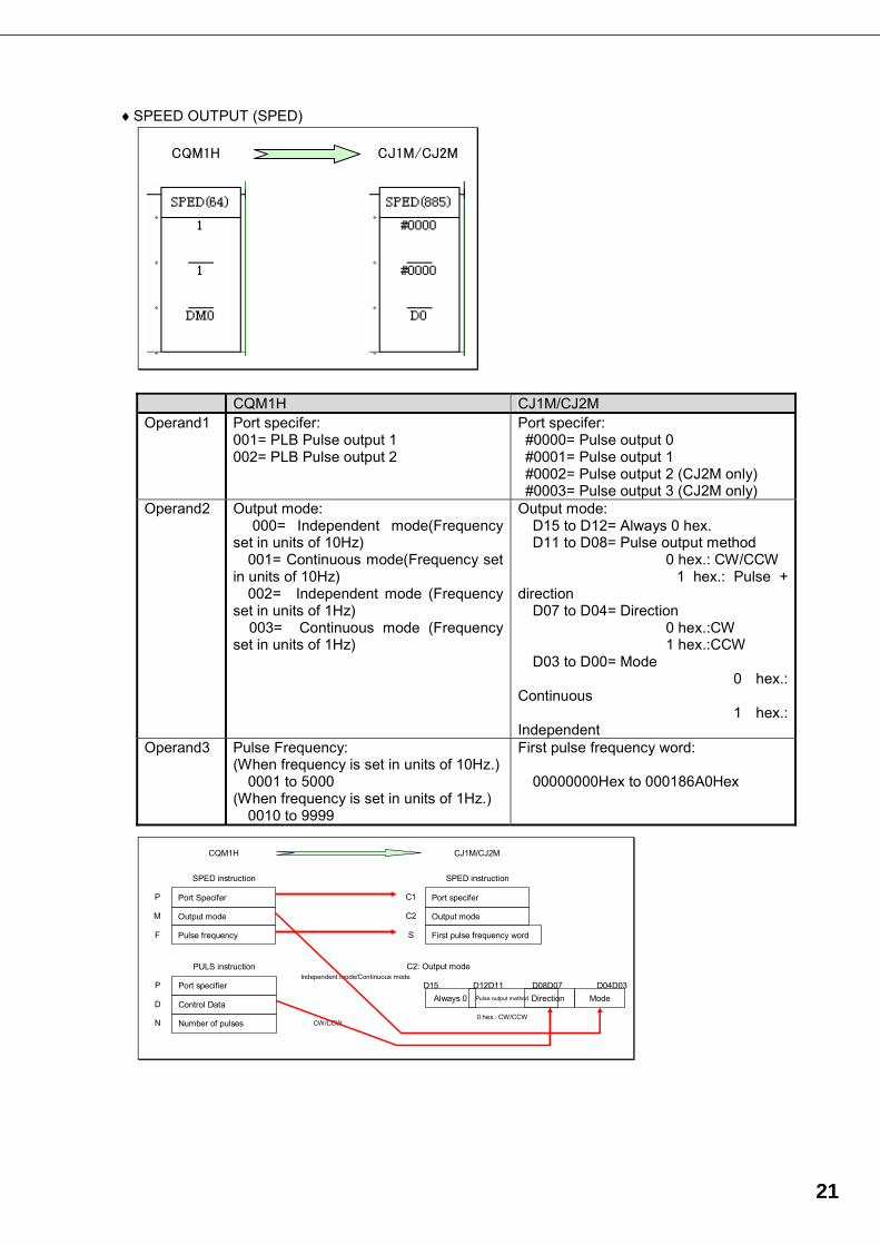
♦SPEED OUTPUT (SPED)
CQM1H CJ1M/CJ2M
CQM1H CJ1M/CJ2M Operand1 Port specifer:
001= PLB Pulse output 1 002= PLB Pulse output 2
Port specifer: #0000= Pulse output 0 #0001= Pulse output 1 #0002= Pulse output 2 (CJ2M only) #0003= Pulse output 3 (CJ2M only)
Operand2 Output mode: 000= Independent mode(Frequency set in units of 10Hz) 001= Continuous mode(Frequency set in units of 10Hz) 002= Independent mode (Frequency set in units of 1Hz) 003= Continuous mode (Frequency set in units of 1Hz)
Output mode: D15 to D12= Always 0 hex. D11 to D08= Pulse output method 0 hex.: CW/CCW 1 hex.: Pulse + direction D07 to D04= Direction 0 hex.:CW 1 hex.:CCW D03 to D00= Mode 0 hex.: Continuous 1 hex.: Independent
Operand3 Pulse Frequency: (When frequency is set in units of 10Hz.) 0001 to 5000 (When frequency is set in units of 1Hz.) 0010 to 9999
First pulse frequency word: 00000000Hex to 000186A0Hex
P
M
Port Specifer
Output mode
Pulse frequency F
CQM1H
Port specifer
Output mode
First pulse frequency word
CJ1M/CJ2M
PULS instruction
Port specifier
Control Data
P
D
C1
C2
S
Always 0 Pulse output method Direction Mode D15 D12D11 D08D07 D04D03
C2: Output mode
N Number of pulses
SPED instruction SPED instruction
Independent mode/Continuous mode
CW/CCW 0 hex.: CW/CCW
21

♦SET PULSES (PULS)
CQM1H CJ1M/CJ2M
CQM1H CJ1M/CJ2M Operand1 Port specifer:
001=PLB Pulse output 1 002=PLB Pulse output 2
Port specifer: #0000= Pulse output 0
#0001= Pulse output 1 #0002= Pulse output 2 (CJ2M only) #0003= Pulse output 3 (CJ2M only)
Operand2 Control Data: 000= CW direction (Number of pulses is set.) 001= CCW direction (Number of pulses is set.) 002= CW direction (Number of pulses and deceleration point are set.) 003= CCW direction (Number of pulses and deceleration point are set.) 004= CW direction (Number of pulses is not set.) 005= CCW direction (Number of pulses is not set.)
Pulse Type: #0000= Relative #0001=Absolute
Operand3 Number of pulses: 00000001 to 16777215
Number of pulses: (When relative pulse is selected.) 00000000Hex to 7FFFFFFFHex (When absolute pulse is selected.) 80000000Hex to 7FFFFFFFHex
P
D
Port specifer
Control Data
Number of pulses N
CQM1H
Port specifer
Pulse type
Number of pulses
CJ1M/CJ2M
C1
C2
S
Always 0 hex. Output method Direction Mode D15 D12D11 D08D07 D04D03
Mode selection
PULS instruction PULS instruction
CW/CCW
Pulse output instructions (SPED, PLS2, ACC)
Relative pulse/
Absolute pulse
22

♦ACCLERATION CONTROL (ACC)
CQM1H CJ1M/CJ2M
CQM1H CJ1M/CJ2M Operand1 Communications port:
001= PLB Pulse output 1 002= PLB Pulse output 2
Port specifer: #0000= Pulse output 0 #0001= Pulse output 1 #0002= Pulse output 2 (CJ2M only) #0003= Pulse output 3 (CJ2M only)
Operand2 Mode specifier: 000=Mode0 (Acceleration + Independent mode) 001=Mode1 (Acceleration + Continuous mode) 002=Mode2 (Deceleration + Independent mode) 003= Mode3 (Deceleration + Continuous mode)
Output mode: D15 to D12= Operation compensation for parameterchanges
0hex.: No operation compensation 4hex.: Operation compensation
D11 to D08= Pulse output method 0hex.: CW/CCW 1hex.: Pulse + direction
D07 to D04= Direction 0hex.:CW 1hex.:CCW
D03 to D00=Mode 0hex.: Continuous mode
1hex.: Independent mode Operand3 First control word:
[T ]Acceleration/Deceleration rate= 0001 to 0200 [T+1]Target frequency =0000 to 5000 [T+2]Deceleration rate =0001 to 0200 [T+3] Frequency after deceleration = 0000 to 5000
First word of settings table: [S ]Acceleration/Deceleration rate = 0001 to FFFFHex [S+1] Lower word with target frequency [S+2]Upper word with target frequency
00000000 to 000186A0hex.
23

P
M
Communications port
Mode specifier: 002
Acceleration/deceleration rate T
CQM1H
Port specifier
Mode specifier
CJ1M/CJ2M
C1
C2
Always 0 Output method Direction Mode D15 D12D11 D08D07 D04D03
PULS instruction
ACC instruction CW/CCW
- Mode2 (Deceleration + Independent mode
ACC instruction
Control Data
Target frequency T+1
PULS instruction
Number of pulses
Port specifer Port specifier
Pulse type
Number of pulses
C1
C2
S
Relative/Absolute
Independent mode
Acceleration/deceleration rate S
Lower word with target frequency
Upper word with target frequency
S+1
S+2
0hex. CW/CCW
24

P
M
Port Specifier
Mode Specifier: 000
Acceleration/Deceleration rate T
CQM1H
Port Specifier
Mode
CJ1M/CJ2M
C1
C2
Always 0Hex Output method Direction Mode D15 D12D11 D08D07 D04D03 D00
PULS instruction
ACC instruction CW/CCW
Mode0 (Accel + Independent mode)
ACC instruction
Control data
Target frequency
Deceleration rate
Frequency after deceleration
T+1
T+2
T+3
PULS instruction
Number of pulses
Port Specifier Port specifier
Pulse type
Number of pulses
C1
C2
S
Relative/Absolute
Independent mode
Acceleration/Deceleration rate S
Lower word with target frequency
Upper word with target frequency
S+1
S+2
*When acceleration/deceleration rate is same.
Frequency after deceleration = Always 0 Hz
*When acceleration/deceleration rate is not same.
P
M
Port Specifier
Mode Specifier: 000
Acceleration/Deceleration rate T
PULS instruction
ACC instruction
Control Data
Target frequency
Deceleration rate
Frequency after deceleration
T+1
T+2
T+3
Number of Pulses
Port Specifier Port Specifier
Output mode
C1
C2
Always 0Hex Output method Direction Mode
PLS2 instruction
D15 D12D11 D08D07 D04D03
Acceleration rate S1
Deceleration rate S1+1
Lower word with target frequency S1+2
Upper word with target frequency S1+3
Pulse output amount (Lower word)
Pulse output amount (Upper word)
S1+4
S1+5
Start frequency (Lower word) S2
Start frequency (Upper word) S2+1
CW/CCW
Independent mode
0Hex:CW/CCW
0Hex:CW/CCW
25

P
M
Port specifier
Mode specifier: 001/003
Acceleration/deceleration rate T
CQM1H
Port specifier
Mode specification
CJ1M/CJ2M
C1
C2
Always 0 Pulse output method Directio Mode D15 D12D11 D08D07 D04D03
PULS instruction
ACC instruction CW/CCW
Mode1 (Acceleration + Continuous mode)/Mode3 (Deceleration + Continuous mode)
ACC instruction
Control Data
Target frequency T+1
Number of pulses
Port specifier
Continuous mode
Acceleration/deceleration rate S
Lower word with target frequency
Upper word with target frequency
S+1
S+2
0 hex.: CW/CCW
26
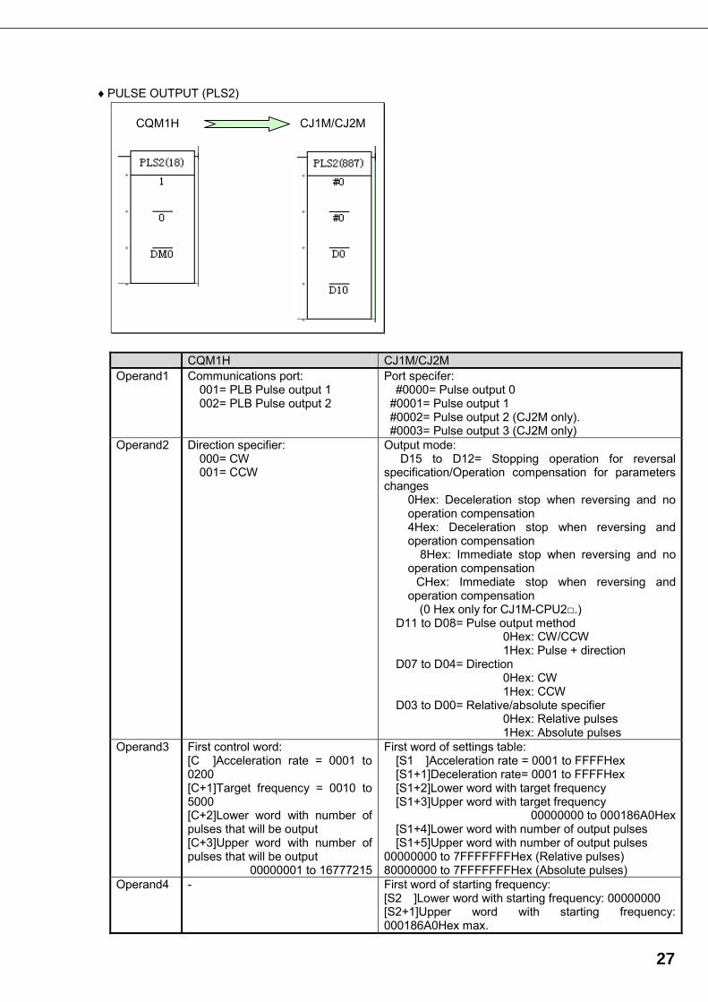
♦PULSE OUTPUT (PLS2)
CQM1H CJ1M/CJ2M
CQM1H CJ1M/CJ2M Operand1 Communications port:
001= PLB Pulse output 1 002= PLB Pulse output 2
Port specifer: #0000= Pulse output 0 #0001= Pulse output 1 #0002= Pulse output 2 (CJ2M only). #0003= Pulse output 3 (CJ2M only)
Operand2 Direction specifier: 000= CW
001= CCW
Output mode: D15 to D12= Stopping operation for reversal specification/Operation compensation for parameters changes
0Hex: Deceleration stop when reversing and no operation compensation 4Hex: Deceleration stop when reversing and operation compensation
8Hex: Immediate stop when reversing and no operation compensation
CHex: Immediate stop when reversing and operation compensation
(0 Hex only for CJ1M-CPU2□.) D11 to D08= Pulse output method 0Hex: CW/CCW 1Hex: Pulse + direction D07 to D04= Direction 0Hex: CW 1Hex: CCW D03 to D00= Relative/absolute specifier 0Hex: Relative pulses 1Hex: Absolute pulses
Operand3 First control word: [C ]Acceleration rate = 0001 to 0200 [C+1]Target frequency = 0010 to 5000 [C+2]Lower word with number of pulses that will be output [C+3]Upper word with number of pulses that will be output
00000001 to 16777215
First word of settings table: [S1 ]Acceleration rate = 0001 to FFFFHex [S1+1]Deceleration rate= 0001 to FFFFHex [S1+2]Lower word with target frequency [S1+3]Upper word with target frequency
00000000 to 000186A0Hex [S1+4]Lower word with number of output pulses [S1+5]Upper word with number of output pulses 00000000 to 7FFFFFFFHex (Relative pulses) 80000000 to 7FFFFFFFHex (Absolute pulses)
Operand4 - First word of starting frequency: [S2 ]Lower word with starting frequency: 00000000 [S2+1]Upper word with starting frequency: 000186A0Hex max.
27

P
D
Communications port
Direction specifier
Accel/Deccel rate C
CQM1H
Port specifier
Mode specifier
CJ1M/CJ2M
C1
C2
Always 0Hex Output method Direction Mode D15 D12D11 D08D07 D04D03 D00
PLS2 instruction
CW/CCW
PLS2 instruction
Target frequency C+1
Acceleration rate S1
Lower word with target frequency
Upper word with target frequency
S1+2
S1+3
0Hex: CW/CCW output
Lower word with number of pulses that will be output
Upper word with number of pulses that will be output
C+2
C+3
0Hex: Relative pulse
Deceleration rate S1+1
Lower word with number of output pulses S1+4
Upper word with number of output pulses S1+5
Lower word with starting frequency
Upper word with starting frequency
S2
S2+1
Starting frequency
28

♦PULSE WITH VARIABLE DUTY FACTOR (PWM)
CQM1H CJ1M/CJ2M
CQM1H CJ1M/CJ2M Operand 1 Communications Port:
001=PLB Pulse Output1 002=PLB Pulse Output 2
Port specifier: <CJ1M-CPU22/23: PWM output 0 and 1 only, CJ1M-CPU21: PWM output 0 only> #0000= PWM output 0 (Frequency unit of 0.1Hz, Duty factor unit of 1%) #0001=PWM output 1(Frequency unit of 0.1Hz, Duty factor unit of 1%) #0002=PWM output 2(Frequency unit of 0.1Hz, Duty factor unit of 1%) #0003=PWM output 3(Frequency unit of 0.1Hz, Duty factor unit of 1%) <CJ1M-CPU Unit version 2.0 or later or CJ2M-CPU only> #1000=PWM output 0 (Frequency unit of 0.1Hz, Duty factor unit of
0.1%) #1001=PWM output1 (Frequency unit of 0.1Hz, Duty factor unit of 0.1%) #1002=PWM output2 (Frequency unit of 0.1Hz, Duty factor unit of 0.1%) #1003=PWM output 3(Frequency unit of 0.1Hz, Duty factor unit of 0.1%) <CJ2M-CPU only> #1100=PWM output 0 (Frequency unit of 1Hz, Duty factor unit of
0.1%) #1101=PWM output 1 (Frequency unit of 1Hz, Duty factor unit of 0.1%) #1102=PWM output 2 (Frequency unit of 1Hz, Duty factor unit of 0.1%) #1103=PWM output 3 (Frequency unit of 1Hz, Duty factor unit of 0.1%)
Operand 2 Frequency: 000= 5.9kHz 001= 1.5kHz 002= 91.6Hz
Frequency: <CJ2M CPU Unit> 0001 to FFFFHex (0.1Hz to 6553.5Hz, Frequency unit of 0.1Hz) 0001 to 8020Hex (1Hz to 32800Hz, Frequency unit of 1Hz) * The ccuracy of PWM wave guaranteed is limited to the range between 0.1 to 1000.0Hz, due to limitation of output circuit. Output accuracy: ON duty +2%, -0% (With 1kHz, 0.5mA output) <CJ1M CPU Unit> 0001 to FFFFHex (0.1Hz to 6553.5Hz, Frequency unit of 0.1Hz) * The ccuracy of PWM wave guaranteed is limited to the range between 0.1 to 1000.0Hz, due to limitation of output circuit.
Output accuracy: ON duty +5%, -0%(With 1kHz 0.5mA output) Operand 3 Duty factor:
0001 to 0099(1 to 99%)Duty factor: 0000 to 0064Hex (0 to 100%) 0000 to 03E8Hex (0 to 100%)
29

5.2 I/O instructions I/O instructions corresponds to the convenient instructions of CQM1H have been added for CJ1M CPU Unit Ver.2.0 or later and CJ2M CPU Unit. A part of specifications of those instructions are different; refer to the table below for details of difference in Operands. The execution time of each instruction is also different; be sure to check the operation for system safery.
♦DIGITAL SWITCH INPUT(DSW)
CQM1H CJ1M/CJ2M
CQM1H CJ1M/CJ2M Operand1 Input word:
D7 to D4:Leftmots 4 digits D3 to D0:Rightmost 4 digits
Input word (Data line inputs(D0 to D3) D7 to D4: Rightmost 4 digits D3 to D0:Leftmost 4 digits
Operand2 Output word: D5: One round flag D4:RD (read) signal (RD0) D3 to D0:CS signal (CS3 to CS0)
Output word (CS/RD control signal outputs) D5: One round flag D4: RD0 Read signal D3 to D0:CS signals (CS3 to CS0)
Operand3 First register word: [R1 ]: Least significant digits (4 digits) [R1+1]:Most significant digits (4 digits)
First Result Word: D15 to D12: Digit 4 D11 to D08: Digit 3 D07 to D04: Digit 2 D03 to D00: Digit 1
Operand4 - Number of digits: [C ] #0000: 4 digits #0001: 8 digits [C+1] System word
Other information CQM1H CJ1M/CJ2M Limitations in number of time used.
Once in one program No limitations
Settings for Number of digits
Set in PC Setup DM6639. 00 (Default) :4 digits, 01: 8 digits
Set in Operand 4.
ER flag operation
- Content of *DM/*EM word is not BCD, or the Em/DM area boundary has been exceeded. (EM can be used with CQM1H-CPU61 only.) - R and R+1 are not in the same data area. (When the CQM1H is set to receive 8-digit data.) - Other than above, ER flag is OFF.
OFF (ER flag does not turn ON with left errors, since they are handled as Illegal access error).
Fun No. 87(Expansion instructions) 210
30

♦TEN KEY INPUT (TKY)
CQM1H CJ1M/CJ2M
CQM1H CJ1M/CJ2M Operand1 Input word:
D09 to D00: Bit00 to 09 works as ten keys (0 to 9).
Input word (Data line inputs): D09 to D00: Bit00 to 09 works as ten keys (0 to 9).
Operand2 First register word: [D1 ]: Least significant 4 digits [D1+1]: Most significant 4 digits
First register word : [D1 ]D15 to D12: Digit 4 D11 to D08: Digit 3 D07 to D04: Digit 2 D03 to D00: Digit 1 [D1+1]D15 to D12: Digit 8 D11 to D08: Digit 7 D07 to D04: Digit 6 D03 to D00: Digit 5
Operand3 Key input word: D10: ON when any key is pressed.
D09 to D00: ON when the corresponding key is pressed. (Remains on until another key
is pressed.)
Key input word: D10: ON when any key is pressed. D09 to D00: ON when the corresponding key is pressed. (Remains on until another key is pressed.)
Other information CQM1H CJ1M/CJ2M Limitations in number of time used.
Can be used twice or more times; however, input word address must be changed.
None
ER flag operation
- Content of *DM/*EM word is not BCD, or the Em/DM area boundary has been exceeded. (EM can be used with CQM1H-CPU61 only.) - D and D+1 are not in the same data area. - Other than above, ER flag is OFF.
OFF (ER flag does not turn ON with left errors, since they are handled as Illegal access error).
Fun No. 18 (Expansion instructions) 211
31

♦HEXADECIMAL KEY INPUT (HKY)
CQM1H CJ1M/CJ2M
CQM1H CJ1M/CJ2M Operand 1 Input word:
Input word (Data line D0 to D3 inputs): D03 to D00: Bits 00 to 03 correspond to Input Unit inputs 0 to 3.
Operand 2 Control signal output word: D03 to D00:16 key selection control signal
Output word (Selection signal output): D03 to D00: Bits 00 to 03 corespond to Output Unit outputs 0 to 3.
Operand 3 First register word: [D1 ]: Least significant 4 digits [D1+1]: Most significant 4 digits [D1+2]: ON when the corresponding key is pressed. (Remains on until another key is pressed.)
First register word: [D1 ]D15 to D12: Digit 4 D11 to D08: Digit 3 D07 to D04: Digit 2 D03 to D00:Digit 1 [D1+1]D15 to D12: Digit 8 D11 to D08: Digit 7 D07 to D04: Digit 6 D03 to D00: Digit 5 [D1+2]D15 to D00: ON when the corresponding key is pressed. (Remains on until another key is pressed.)
Operand 4 - System word: Other infotmation CQM1H CJ1M/CJ2M Limitations in number of time used.
Once in one program No limitations
ER flag operation
- Content of *DM/*EM word is not BCD, or the EM/DM area boundary has been exceeded. (EM can be used with CQM1H-CPU61 only.) - R and R+1 are not in the same data area. - Other than above, ER flag is OFF.
OFF (ER flag does not turn ON with left errors, since they are handled as Illegal access error).
Fun No. --- (Expansion instruction) 212
32

♦7-SEGMENT DISPLAY OUTPUT (7SEG) CQM1H CJ1M/CJ2M
CQM1H CJ1M/CJ2M Operand1 First source word:
[S1 ]: Rightmost 4 digits [S1+1]: Leftmost 4 digits
Source word: [S1 ]D15 to D12: Digit 4 D11 to D08: Digit 3 D07 to D04: Digit 2 D03 to D00: Digit 1 [S1+1]D15 to D12: Digit 8 D11 to D08: Digit 7 D07 to D04: Digit 6 D03 to D00: Digit 5
Operand2 Output word: Converting 4 digits D08:One round flag D07 to D04: Latch output LE3 to LE0 D03 to D00: 4-digit data output Converting 8 digits
D12: One round flag D11 to D08:Latch output LE3 to LE0 D07 to D04:Rightmost 4-digit data output
D03 to D00: Leftmost 4-digit data output
Output word (Data and latch outputs): Converting 4 digits D08:One round flag D07 to D04: Latch output LE3 to LE0 D03 to D00: 4-digit data output Converting 8 digits
D12: One round flag D11 to D08:Latch output LE3 to LE0 D07 to D04:Rightmost 4-digit data output D03 to D00: Leftmost 4-digit data output
Operand3 Control data: Data Source
data Display’s data Input logic
Display’s katch input logic
000 Same as Output Unit
001
Same as Output Unit
Different from Output Unit
002 Same as Output Unit
003
4 digits (4 digits x 1)
Different from Output Unit Different
from Output Unit
004 Same as Output Unit
005
Same as Output Unit
Different from Output Unit
006 Same as Output Unit
007
8 digits (8 digit x 1)
Different from Output Unit Different
from Output Unit
Control data: Data Source
data Display’s data Input logic
Display’s katch input logic
000 Same as Output Unit
001
Same as Output Unit
Different from Output Unit
002 Same as Output Unit
003
4 digits (4 digits x 1)
Different from Output Unit Different
from Output Unit
004 Same as Output Unit
005
Same as Output Unit
Different from Output Unit
006 Same as Output Unit
007
8 digits (4 digits x 2)
Different from Output Unit Different
from Output Unit
33

Operand4 - System word:
Other information CQM1H CJ1M/CJ2M Limitations in number of time used.
Once in one program. No limitations
ER flag operation
- Content of *DM/*EM word is not BCD, or the EM/DM area boundary has been exceeded. (EM can be used with CQM1H-CPU61 only.) - S and S+1 are not in the same data area. (When set to display 8-digit data.) - There is an error in operand settngs - Other than above, ER flag is OFF.
OFF (ER flag does not turn ON with left errors, since they are handled as Illegal access error).
Fun No. 88 (Expansion instruction) 214
34

5.3 Model conversion instructions
The model conversion instructions (below five instructions) which were added for CJ1M CPU Unit Ver. 3.0 or later can be used with CJ2M CPU Units in the same way as CQM1H series CPU Units. Those instructions are automatically converterd by executing change model (from CQM1H to CJ2M) on the CX-Programmer Ver.5 or later (CX-Programmer Ver.5 or later supports functions of CJ1M CPU Unit Ver. 3.0). Be sure to check the operation, since operation specifications including instruction execution time might differ.
Instructions Model conversion instruction
(CJ1M CPU Unit Ver.3.0 or later and CJ2M CPU Units)
Corresponding instruction for CQM1H
BLOCK TRANSFER
XFERC (565) XFER (70)
SINGLE WORD DISTRIBUTE
DISTC (566) DIST (80)
hDATA COLLECT COLLC (567) COLL (81) MOVE BIT MOVBC (568) MOVB (82)
BIT COUNTER BCNTC (621) BCNT (67)
35

6. Example of converting ladder program by CX-Programmer
This section explains the method of converting the ladder program using CX-Programmer V9.1. Here, convert the ladder program of CQM1H-CPU61 for CJ2M-CPU** as an example. (This secrion describes the procedure from loading the ladder program created by CX-Programmer or Sysmac Support Soft (SSS) to converting the program for CJ2M.) After converting the ladder program, it is necessary to modify the unit area allocation, operand data, and condition flag settings, separately. Be sure to confirm the system safety before starting operation. ♦Reading the ladder program of CQM1H
・SSS data
On the CX-Programmer, select File – Open. Set the file type to “SSS Ladder Program (*.SP1)” and open the SSS ladder program file for CQM1H. On the below dialog, Click the “Open”.
Then, dialog box to enter the model of CQM1 CPU Unit will be displayed. Enter the model of the CPU Unit. (For CQM1H, select corresponding CQM1 model.)
・CX-Programmer data
Click the "File" - "Open" and set the file type to CX-Programmer Project Files (*.cxp)". Then, open the ladder program file of CQM1H created on the CX-Programmer.
36

37
♦Changing model from CQM1H to CJ2M. As shown on the below figure, select NewPLC1[CQM1H] and right-click or double click it to change the PLC model. Please set the CPU model to the Device Type. The error report might be displayed if there are instructions which cannot be converted. Please correct and modify the program using support software function or manually, and execute program check. If errors are detected by the program check, please correct them referring to the error report.
Right-click and select
“Change” or double-click.
♦Checking program Check whether there is problem in the ladder program which was converted from the CQM1H series for CJ2M series.
Program check There are 2 types of program check; automatic check on the CX-Programmer and check conducted by users. CX-Programmer checks the program when “Change model” is executed and the ledder program is converted. • Automatic program check on the CX-Programmer
Timing of program check Description When PLC model is changed. Program check for each PLC model
Check for all instructions and all operands. You can see the check result on the "Compile (Program check)" tab of the Output Window. The left bus-bar on the ladder section window turns red if there is an error in the rung. • Program check conducted by users
This section describes the procedure of program check, an example of checking result, and explanation of error levels.
<Program check for one program (task)> 1. Select the ladder section window or nimonic window to check. 2. Select “Program” – “Compile (Program check)”.
The results of program check will be displayed on the Output Window. Refer to “Results of program check” on the next page for details.
38

• Checking the entire program Select “PLC” – “Compile All PLC Programs”.
You can see the program check results on the Output Window. Refer to “Results of program check” for details.
<Results of program check> You can see the check result on the "Compile (Program check)" tab of the Output Window.
There are three error levels; errors are divided and shown for each level. When there is no error.
When there are errors.
Double-click an error on the Output Window to jump to the correposnding cell. Numeric data in ( , ) shows the position of a cell with an error. If you right-click on the Output Window, below menus are shown.
Menu Functions [Clear] Clears the content of Output Window.
Same as selecting “Edit” – “Clear Compile Window”. [Next Reference] Jump to the error cell next to the error now selected.
Same as selecting “Edit” – “Next Reference”. [Allow Docking] Output Window is shown on the main window of the
CX-Programmer. If unckeck the check box, Output Window will be shown on the separate window.
[Hide] Close the output window. Same as selecting “View” – “Window” – “Output”.
[Float In Main Window] Output window will be changed to other window (ex. Ladder section window).
39

Appendix A-1 Instruction operations
Conversion: **= Support software converts the instruction./*= Support software converts the instruction, but it is necessary to manually modify it. /- = There is no corresponding instruction.Blank cells: Support software converts the instructions, though there are some difference in CQM1H/CJ1M/CJ1G and CJ2M.
Instructions CQM1H Conversion Nemonic FUN No. Number of operand BCD => BIN Settings RemarksSequence input instructions
LOAD LD LD **LOAD NOT LD NOT LD NOT **AND AND AND **AND NOT AND NOT AND NOT **OR OR OR **OR NOT OR NOT OR NOT ** AND LOAD AND LD AND LD **OR LOAD OR LD OR LD **
Sequence output instructionsOUTPUT OUT OUT **OUTPUT NOT OUT NOT OUT NOT **TR Bits TR TR **KEEP KEEP KEEP **DIFFERENTIATE UP DIFU DIFU **DIFFERENTIATE DOWN DIFD DIFD **SET SET SET **RESET RSET RSET **
Sequence control instructionsEND END END **NO OPERATION NOP NOP **INTERLOCK IL IL **INTERLOCK CLEAR ILC ILC **JUMP JMP JMP ** Jump No.JUMP END JME JME ** Jump No.
Timer and counter instructionsTIMER TIM TIM **HIGH-SPEED TIMER TIMH TIMH **TOTALIZING TIMER TTIM TTIM * Expansion ->87 Operand3: reset input
relay No will be deleted.Enter the reset input.
COUNTER CNT CNT **REVERSIBLE COUNTER CNTR CNTR **
Comparison instructionsCOMPARE CMP CMP **DOUBLE COMPARE CMPL CMPL ** Expansion ->60 3 (None)->2SIGNED BINARY COMPARE CPS CPS ** Expansion ->114 3 (None)->2DOUBLE SIGNED BINARY COMPARE CPSL CPSL ** Expansion ->115 3 (None)->2MULTI-WORD COMPARE MCMP MCMP **TABLE COMPARE TCMP TCMP **BLOCK COMPARE BCMP BCMP **AREA RANGE COMPARE ZCP ZCP Expansion ->88DOUBLE AREA RANGE COMPARE ZCPL ZCPL Expansion ->116
Data movement instructionsMOVE MOV MOV **MOVE NOT MVN MVN **MOVE BIT MOVB MOVB * Change bit position
specification from inBCD to in BIN.
MOVBC[Ver.3.0 orlater]
** 82->568
MOVE DIGIT MOVD MOVD **TRANSFER BITS XFRB XFRB ** Expansion ->62BLOCK TRANSFER XFER XFER * Number of words:
BCD -> BINXFERC[Ver.3.0 orlater]
** 70->565
BLOCK SET BSET BSET **DATA EXCHANGE XCHG XCHG **SINGLE WORD DISTRIBUTE DIST DIST * Stack length data set
in words: BCD -> BINUse PUSH instructioninstead, for stackoperation.
DISTC[Ver.3.0 orlater]
** 80->566
DATA COLLECT COLL COLL * Stack length data setin words: BCD -> BIN
Use FIFO instructioninstead, for stackoperation and readFIFO.Use LIFO instructioninstead, for stackoperation and readLIFO.
COLLC[Ver.3.0 or
** 81->567
Data shift instructionsSHIFT REGISTER SFT SFT **REVERSIBLE SHIFT REGISTER SFTR SFTR **ASYNCHRONOUS SHIFT REGISTER ASFT ASFT **WORD SHIFT WSFT WSFT * 2->3 Set the shift sata in
the Operand 1.ARITHMETIC SHIFT LEFT ASL ASL **ARITHMETIC SHIFT RIGHT ASR ASR **ROTATE LEFT ROL ROL **ROTATE RIGHT ROR ROR **ONE DIGIT SHIFT LEFT SLD SLD **ONE DIGIT SHIFT RIGHT SRD SRD **
Increment/ decrement instructionsINCREMENT INC ++B ** INC->++B 38->594BCD DECREMENT DEC --B ** DEC->--B 39->596
Symbol math instructionsBINARY ADD ADB +C ** ADB->+C 50->402DOUBLE BINARY ADD ADBL +CL ** ADBL->+CL Expansion ->403BCD ADD ADD +BC ** ADD->+BC 30->406DOUBLE BCD ADD ADDL +BCL ** ADDL->+BCL 54->407BINARY SUBTRACT SBB -C ** SBB->-C 51->412DOUBLE BINARY SUBTRACT SBBL -CL ** SBBL->-CL Expansion ->413BCD SUBTRACT SUB -BC ** SUB->-BC 31->416DOUBLE BCD SUBTRACT SUBL -BCL ** SUBL->-BCL 55->417SIGNED BINARY MULTIPLY MBS * ** MBS->* Expansion ->420DOUBLE SIGNED BINARY MULTIPLY MBSL *L ** MBSL->*L Expansion ->421BINARY MULTIPLY MLB *U ** MLB->*U 52->422BCD MULTIPLY MUL *B ** MUL->*B 32->424DOUBLE BCD MULTIPLY MULL *BL ** MULL->*BL 56->425SIGNED BINARY DIVIDE DBS / ** DBS->/ Expansion ->430DOUBLE SIGNED BINARY DIVIDE DBSL /L ** DBSL->/L Expansion ->431BINARY DIVIDE DVB /U ** DVB->/U 53->432BCD DIVIDE DIV /B ** DIV->/B 33->434DOUBLE BCD DIVIDE DIVL /BL ** DIVL->/BL 57->435
Difference between CQM1H and CJ1M/CJ1G/CJ2M (CQM1H->CJ1M/CJ1G/CJ2M)CJ1M/CJ1G
1

Appendix A-1 Instruction operations
Conversion: **= Support software converts the instruction./*= Support software converts the instruction, but it is necessary to manually modify it. /- = There is no corresponding instruction.Blank cells: Support software converts the instructions, though there are some difference in CQM1H/CJ1M/CJ1G and CJ2M.
Instructions CQM1H Conversion Nemonic FUN No. Number of operand BCD => BIN Settings RemarksDifference between CQM1H and CJ1M/CJ1G/CJ2M (CQM1H->CJ1M/CJ1G/CJ2M)CJ1M/CJ1
GConversion instructions
BCD-TO-BINARY BIN BIN **DOUBLE BCD-TO-DOUBLE BINARY BINL BINL **BINARY TO BCD BCD BCD **DOUBLE BINARY-TO-DOUBLE BCD BCDL BCDL **2’S COMPLEMENT NEG NEG ** Expansion ->160 3 (None)->2DOUBLE 2’S COMPLEMENT NEGL NEGL ** Expansion ->161 3 (None)->24-TO-16 DECODER MLPX MLPX **16-TO-4 ENCODER DMPX DMPX **ASCII CONVERT ASC ASC **ASCII-TO-HEXADECIMAL HEX HEX ** Expansion ->162LINE LINE LINE * Expansion ->63 Bit number set in
words: BCD -> BINLINE TO COLUMN COLM COLM * Expansion ->64 Bit number set in
words: BCD -> BINLogic instructions
LOGICAL AND ANDW ANDW **LOGICAL OR ORW ORW **EXCLUSIVE OR XORW XORW **EXCLUSIVE NOR XNRW XNRW **COMPLEMENT COM COM **
Special math instructionsBSQUARE ROOT ROOT ROOT **ARITHMETIC PROCESS APR APR ** Expansion ->69BIT COUNTER BCNT BCNT * Number of words set
in words: BCD -> BINBCNTC[Ver.3.0 orlater]
** 67->621
Floating point math instructionsFLOATING TO 16-BIT FIX FIX ** Expansion ->450 3 (None)->2FLOATING TO 32-BIT FIXL FIXL ** Expansion ->451 3 (None)->216-BIT TO FLOATING FLT FLT ** Expansion ->452 3 (None)->232-BIT TO FLOATING FLTL FLTL ** Expansion ->453 3 (None)->2FLOATING-POINT ADD +F +F ** Expansion ->454FLOATING-POINT SUBTRACT -F -F ** Expansion ->455FLOATING-POINT MULTIPLY *F *F ** Expansion ->456FLOATING-POINT DIVIDE /F /F ** Expansion ->457DEGREES TO RADIANS RAD RAD ** Expansion ->458 3 (None)->2RADIANS TO DEGREES DEG DEG ** Expansion ->459 3 (None)->2SINE SIN SIN ** Expansion ->460 3 (None)->2COSINE COS COS ** Expansion ->461 3 (None)->2TANGENT TAN TAN ** Expansion ->462 3 (None)->2ARC SINE ASIN ASIN ** Expansion ->463 3 (None)->2ARC COSINE ACOS ACOS ** Expansion ->464 3 (None)->2ARC TANGENT ATAN ATAN ** Expansion ->465 3 (None)->2SQUARE ROOT SQRT SQRT ** Expansion ->466 3 (None)->2EXPONENT EXP EXP ** Expansion ->467 3 (None)->2LOGARITHM LOG LOG ** Expansion ->468 3 (None)->2
Table data processing instructionsDATA SEARCH SRCH SRCH * Expansion ->181 Number of words set
in words: BCD -> BINOutput selection toenable or disable theOutputs number ofmatches.
Operand1: 1 word -> 2wordsComparison data,result word: C+1 ->
FIND MAXIMUM MAX MAX * Expansion ->182 Number of words inrange: BCD -> BIN,Settings 12 bits -> 15bits
Select signed orunsigned/Outputsaddress to IR or not.
Control data: 1word ->2 wordOutput address: D+1 -> IR00
FIND MINIMUM MIN MIN * Expansion ->183 Number of words inrange: BCD -> BIN,Settings 12 bits -> 15bits
Select signed orunsigned/Outputsaddress to IR or not.
Control data: 1word ->2 wordOutput address: D+1 -> IR00
SUM SUM SUM * Expansion ->184 table length: BCD ->BIN, Settings 12 bits -> 15 bits
Set the Startingbyte/Units/Datatype/signed or not inC+1.
Control data: 1word ->2 word
FCS CALCULATE FCS FCS * Expansion ->180 table length: BCD ->BIN, Settings 12 bits -> 15 bits
Set the Startingbyte/Units in C+1.
Control data: 1word ->2 word
Data control instructionsPID CONTROL PID PID * Expansion ->190 Set value: BCD -> BIN Check setting items
and set value.PID parameter area:33ch -> 39ch
SCALING SCL SCL * 66->194 Acaled value: variableaccepted -> variablenot accepted
SIGNED BINARY TO BCD SCALING SCL2 SCL2 ** Expansion ->486BCD TO SIGNED BINARY SCALING SCL3 SCL3 ** Expansion ->487AVERAGE VALUE AVG AVG * Expansion ->195 Number of cycles set
in words: BCD -> BINAverage Valid Flag:None -> Processinginformation D15 bit
Subroutines instructionsSUBROUTINE ENTRY SBS SBS **MACRO MCRO MCRO ** Macro area input
words: 96 to 99 ->A600 to A603, 196 to199 -> A604 to A607(No influence on theladder program).
SUBROUTINE DEFINE SBN SBN **SUBROUTINE RETURN RET RET **
Interrupt control instructionsINTERRUPT CONTROL INT MSKS
MSKRCLIDIEI
* INT000->MSKSINT001->CLIINT002->MSKRINT003->MSKS/INI(CJ1M built-in inputonly) INT100->DIINT200->EI
89->69089->69189->69289->690/880
89->69389->694
Interrupt unit/CJ1Mbuilt-in interrupt input:newly configure thesettings.
Interrupt program:interrupt subroutine ->interrupt task (Alsochange the numberagain).
INTERVAL TIMER STIM MSKSMSKR
* (Partly "-")Instructionwill not be
converted iftimer
start/stoptime is
specified.
STIM003 to 005->MSKSSTIM006 to 008->MSKR
69->69069->692
Set the operands inBCD ->BIN.
Newly configure thesettings again.
One-shot interruptstart: NoneStopping timerfunction: NoneSet the unit of 0.1msin PLC settings.Interrupt program:interrupt subroutine ->interrupt task (Newlyset the task No.)
Step instructionsSTEP DEFINE STEP STEP **STEP START SNXT SNXT **
2

Appendix A-1 Instruction operations
Conversion: **= Support software converts the instruction./*= Support software converts the instruction, but it is necessary to manually modify it. /- = There is no corresponding instruction.Blank cells: Support software converts the instructions, though there are some difference in CQM1H/CJ1M/CJ1G and CJ2M.
Instructions CQM1H Conversion Nemonic FUN No. Number of operand BCD => BIN Settings RemarksDifference between CQM1H and CJ1M/CJ1G/CJ2M (CQM1H->CJ1M/CJ1G/CJ2M)CJ1M/CJ1
GBasic I/O Unit instructions
I/O REFRESH IORF IORF **7-SEGMENT DECODER SDEC SDEC **7-SEGMENT DISPLAY OUTPUT 7SEG 7SEG
[Ver.2.0 orlater]
* 3->4 Set the address of Firstdestination word.
DIGITAL SWITCH DSW DSW[Ver.2.0 orlater]
* 3->5 Set the Number ofDigits and SystemWord.
TEN KEY INPUT TKY TKY[Ver.2.0 orlater]
**
HEXADECIMAL KEY INPUT HKY HKY[Ver.2.0 orlater]
* 3->4 Set the first registerword.
IO COMMAND TRANSMISSION IOTC - ×Serial communications instructions
PROTOCOL MACRO PMCR PMCR * Expansion ->260 3->4 Send/Receivesequence No.: BCD ->BINNumber ofsend/receive words:BCD -> BIN
Set thecommunicaitons portand destination unitaddress.Enter the send/receivesequence No in theOperand2 (C2).
Change related relaysettings.
TRANSMIT TXD TXD * 48->236 Number of bytesspedifies in words:BCD -> BIN
Peripheral port/serialcommunication cannot be selected forport spedifier.Change related relaysettings.
RECEIVE RXD RXD * 47->235 Number of bytes tostore specified inwords: BCD -> BIN
Peripheral port/serialcommunication cannot be selected forport spedifier.Change related relaysettings.
CHANGE SERIAL PORT SETUP STUP STUP * Expansion ->237 3->2 Port specificationmethod is changed.
Settings after turningoff/on power: stored ->resetchange the relatedrelay settings.
Network instructionsNETWORK SEND SEND SEND * Set the control data
again.Control data: 4 words -> 5 wordsChange related relays.
NETWORK RECEIVE RECV RECV * Set the control dataagain.
Control data: 4 words -> 5 wordsChange related relays.
DELIVER COMMAND CMND CMND * Expansion ->490 Set the control dataagain.
Control data: 5 words -> 6 wordsChange related relays.
Display instructionsMESSAGE MSG MSG * 1->2 Set the message
number in theOperand1.
Clock instructionsHOURS TO SECONDS SEC SEC ** Expansion ->65 3 (None)->2SECONDS TO HOURS HMS HMS ** Expansion ->66 3 (None)->2
Debugging instructionsTRACE MEMORY SAMPLE TRSM TRSM ** Change related relays.
Failure diagnosis instructionsFAILURE ALARM AND RESET FAL FAL * 1->2 In Operand, enter
FAL00: Clears thenon-fatal error with thecorresponding FALnumber.Not FAL00: Word tosend message or Errorcode to generate orword containing theerror details
SEVERE FAILURE ALARM FALS FALS * 1->2 In Operand2, set Firstmessage word or errorcode and error details
FAILURE POINT DETECT FPD FPD * Monitoring timespedified in words:BCD ->BIN
Configure the operandsagain if diagnositicoutput mode is set inBit address andmessage output.
Output area:When output in codes= 2 words -> 4 wordsWhen output incharacter =9 words ->10 words
Other instructionsSET CARRY STC STC **CLEAR CARRY CLC CLC **
High-speed counter/pulse output instructionsMODE CONTROL INI INI * 61->880 First word with new
PV: BCD ->BINRefer to 5.1 High-speed counter/pulseoutput instruction.
HIGH-SPEED COUNTER PV READ PRV PRV * 62->881 PV output in BCD ->BIN.
Refer to 5.1 High-speed counter/pulseoutput instruction.
Configure the referenceposition of status data.
COMPARISON TABLE LOAD CTBL CTBL * 63->883 Number of targetvalues/targetvalue/Interrupt tasknumber: BCD -> BIN
Refer to 5.1 High-speed counter/pulseoutput instruction.
In Ring mode, enterthe ring value in thePLC settings.Interrupt program:interrupt subroutine ->interrupt task (Alsochange the task No.).
SET PULSES PULS PULS * 65->886 Number of pulses:BCD -> BIN
Refer to 5.1 High-speed counter/pulseoutput instruction.
SPEED OUTPUT SPED SPED * 64->885 Target frequencyspecified in words:BCD -> BIN
Refer to 5.1 High-speed counter/pulseoutput instruction.
ACCELERATION CONTROL ACC ACC * Expansion ->888 Acceleration/deceleration rate/targetfrequency: BCD -> BIN
Refer to 5.1 High-speed counter/pulseoutput instruction.
PULSE OUTPUT PLS2 PLS2 * Expansion ->887 3->4 Acceleration/deceleration rate/targetfrequency/number ofoutput pulses: BCD ->BIN
Refer to 5.1 High-speed counter/pulseoutput instruction.
PULSE WITH VARIABLE DUTY FACTOR PWM PWM * Expansion ->891 Duty factor specified inwords: BCD ->BIN
Refer to 5.1 High-speed counter/pulseoutput instruction.
3

Appendix A-2 Condition flag operations
Conversion: *** = same condition flag operation, ** = a part of condition flag operation differs, - = Different condition flag operation, None = no corresponding instructionCondition flags: Left of "/"= Operation of CQM1H. Right of "/"= Operation of CJ1M/CJ1G/CJ2M No "/" = Same operation in CQM1H and CJ
*= ON/OFF depending on the instruction statuusCJ1M/CJ1G
Instructions CQM1H /CJ2M Conversion ER GT(>) GE(CJ)
EQ(=) NE (CJ) LT(<) LE(CJ) CY UF OF N (CJ)
Sequence input instructionsLOAD LD LD ***LOAD NOT LD NOT LD NOT ***AND AND AND ***AND NOT AND NOT AND NOT ***OR OR OR ***OR NOT OR NOT OR NOT *** AND LOAD AND LD AND LD ***OR LOAD OR LD OR LD ***
Sequence output instructionsOUTPUT OUT OUT ***OUTPUT NOT OUT NOT OUT NOT ***TR Bits TR TR ***KEEP KEEP KEEP ***DIFFERENTIATE UP DIFU DIFU ***DIFFERENTIATE DOWN DIFD DIFD ***SET SET SET ***RESET RSET RSET ***
Sequence control instructionsEND END END - OFF/ OFF/ OFF/ OFF/ OFF/ OFF/ OFF/NO OPERATION NOP NOP ***INTERLOCK IL IL ***INTERLOCK CLEAR ILC ILC ***JUMP JMP JMP - /*JUMP END JME JME ***
Timer and counter instructionsTIMER TIM TIM *** *HIGH-SPEED TIMER TIMH TIMH *** *TOTALIZING TIMER TTIM TTIM *** *COUNTER CNT CNT *** *REVERSIBLE COUNTER CNTR CNTR *** *
Comparison instructionsCOMPARE CMP CMP ** * * /* * /* * /*DOUBLE COMPARE CMPL CMPL ** * * /* * /* * /*SIGNED BINARY COMPARE CPS CPS ** * * /* * /* * /*DOUBLE SIGNED BINARY COMPARE CPSL CPSL ** * * /* * /* * /*MULTI-WORD COMPARE MCMP MCMP *** * *TABLE COMPARE TCMP TCMP ** */OFF *BLOCK COMPARE BCMP BCMP ** * /*AREA RANGE COMPARE ZCP ZCP *** * * * *DOUBLE AREA RANGE COMPARE ZCPL ZCPL *** * * * *
Data movement instructionsMOVE MOV MOV ** * * /*MOVE NOT MVN MVN ** * * /*MOVE BIT MOVB MOVB *** *
MOVBC[Ver.3.0or later]
*** *
MOVE DIGIT MOVD MOVD *** *TRANSFER BITS XFRB XFRB - */OFFBLOCK TRANSFER XFER XFER - */OFF
XFERC[Ver.3.0or later]
*** *
BLOCK SET BSET BSET *** *DATA EXCHANGE XCHG XCHG - */SINGLE WORD DISTRIBUTE DIST DIST ** */OFF * /*
DISTC[Ver.3.0or later]
** * * /*
DATA COLLECT COLL COLL ** */OFF * /*COLLC[Ver.3.0or later]
** * * /*
Data shift instructionsSHIFT REGISTER SFT SFT - /*REVERSIBLE SHIFT REGISTER SFTR SFTR *** * *ASYNCHRONOUS SHIFT REGISTER ASFT ASFT *** *WORD SHIFT WSFT WSFT *** *ARITHMETIC SHIFT LEFT ASL ASL ** */OFF * * /*ARITHMETIC SHIFT RIGHT ASR ASR ** */OFF * * */OFFROTATE LEFT ROL ROL ** */OFF * * /*ROTATE RIGHT ROR ROR ** */OFF * * /*ONE DIGIT SHIFT LEFT SLD SLD *** *ONE DIGIT SHIFT RIGHT SRD SRD *** *
Increment/ decrement instructionsINCREMENT INC ++B ** * * /*BCD DECREMENT DEC --B ** * * /*
Condition flags ( (CJ) = CQM1H does not have this settings.)
4
Appendix A-2 Condition flag operations
Conversion: *** = same condition flag operation, ** = a part of condition flag operation differs, - = Different condition flag operation, None = no corresponding instructionCondition flags: Left of "/"= Operation of CQM1H. Right of "/"= Operation of CJ1M/CJ1G/CJ2M No "/" = Same operation in CQM1H and CJ
*= ON/OFF depending on the instruction statuusCJ1M/CJ1G
Instructions CQM1H /CJ2M Conversion ER GT(>) GE(CJ)
EQ(=) NE (CJ) LT(<) LE(CJ) CY UF OF N (CJ)Condition flags ( (CJ) = CQM1H does not have this settings.)
Symbol math instructionsBINARY ADD ADB +C ** */OFF * * * * /*DOUBLE BINARY ADD ADBL +CL ** */OFF * * * * /*BCD ADD ADD +BC *** * * *DOUBLE BCD ADD ADDL +BCL *** * * *BINARY SUBTRACT SBB -C ** */OFF * * * * /*DOUBLE BINARY SUBTRACT SBBL -CL ** */OFF * * * * /*BCD SUBTRACT SUB -BC *** * * *DOUBLE BCD SUBTRACT SUBL -BCL *** * * *SIGNED BINARY MULTIPLY MBS * ** */OFF * /*DOUBLE SIGNED BINARY MULTIPLY MBSL *L ** */OFF * /*BINARY MULTIPLY MLB *U ** */OFF * /*BCD MULTIPLY MUL *B *** * *DOUBLE BCD MULTIPLY MULL *BL *** * *SIGNED BINARY DIVIDE DBS / ** * * /*DOUBLE SIGNED BINARY DIVIDE DBSL /L ** * * /*BINARY DIVIDE DVB /U ** * * /*BCD DIVIDE DIV /B *** * *DOUBLE BCD DIVIDE DIVL /BL *** * *
Conversion instructionsBCD-TO-BINARY BIN BIN ** * * */OFFDOUBLE BCD-TO-DOUBLE BINARY BINL BINL ** * * */OFFBINARY TO BCD BCD BCD *** * *DOUBLE BINARY-TO-DOUBLE BCD BCDL BCDL *** * *2’S COMPLEMENT NEG NEG ** */OFF * */ /*DOUBLE 2’S COMPLEMENT NEGL NEGL ** */OFF * */ /*4-TO-16 DECODER MLPX MLPX *** *16-TO-4 ENCODER DMPX DMPX *** *ASCII CONVERT ASC ASC *** *ASCII-TO-HEXADECIMAL HEX HEX *** *LINE LINE LINE *** * *LINE TO COLUMN COLM COLM *** * *
Logic instructionsLOGICAL AND ANDW ANDW ** */OFF * /*LOGICAL OR ORW ORW ** */OFF * /*EXCLUSIVE OR XORW XORW ** */OFF * /*EXCLUSIVE NOR XNRW XNRW ** */OFF * /*COMPLEMENT COM COM ** */OFF * /*
Special math instructionsBSQUARE ROOT ROOT ROOT *** * *ARITHMETIC PROCESS APR APR ** * * /*BIT COUNTER BCNT BCNT *** * *
BCNTC[Ver.3.0or later]
*** * *
Floating point math instructionsFLOATING TO 16-BIT FIX FIX ** * * /*FLOATING TO 32-BIT FIXL FIXL ** * * /*16-BIT TO FLOATING FLT FLT ** */ * /*32-BIT TO FLOATING FLTL FLTL ** */ * /*FLOATING-POINT ADD +F +F ** * * * * /*FLOATING-POINT SUBTRACT -F -F ** * * * * /*FLOATING-POINT MULTIPLY *F *F ** * * * * /*FLOATING-POINT DIVIDE /F /F ** * * * * /*DEGREES TO RADIANS RAD RAD ** * * * * /*RADIANS TO DEGREES DEG DEG ** * * * * /*SINE SIN SIN ** * * OFF/ OFF/ /*COSINE COS COS ** * * OFF/ OFF/ /*TANGENT TAN TAN ** * * OFF/ * /*ARC SINE ASIN ASIN ** * * OFF/ OFF/ /*ARC COSINE ACOS ACOS ** * * OFF/ OFF/ARC TANGENT ATAN ATAN ** * * OFF/ OFF/ /*SQUARE ROOT SQRT SQRT ** * * OFF/ *EXPONENT EXP EXP *** * * * *LOGARITHM LOG LOG ** * * OFF/ * /*
Table data processing instructionsDATA SEARCH SRCH SRCH *** * *FIND MAXIMUM MAX MAX ** * * /*FIND MINIMUM MIN MIN ** * * /*SUM SUM SUM ** * * /*FCS CALCULATE FCS FCS *** *
Data control instructionsPID CONTROL PID PID ** * /* /* *SCALING SCL SCL *** * *SIGNED BINARY TO BCD SCALING SCL2 SCL2 *** * * *BCD TO SIGNED BINARY SCALING SCL3 SCL3 *** * * /*AVERAGE VALUE AVG AVG *** *
Subroutines instructionsSUBROUTINE ENTRY SBS SBS *** *MACRO MCRO MCRO *** *SUBROUTINE DEFINE SBN SBN ***SUBROUTINE RETURN RET RET ***
5

Appendix A-2 Condition flag operations
Conversion: *** = same condition flag operation, ** = a part of condition flag operation differs, - = Different condition flag operation, None = no corresponding instructionCondition flags: Left of "/"= Operation of CQM1H. Right of "/"= Operation of CJ1M/CJ1G/CJ2M No "/" = Same operation in CQM1H and CJ
*= ON/OFF depending on the instruction statuusCJ1M/CJ1G
Instructions CQM1H /CJ2M Conversion ER GT(>) GE(CJ)
EQ(=) NE (CJ) LT(<) LE(CJ) CY UF OF N (CJ)Condition flags ( (CJ) = CQM1H does not have this settings.)
Interrupt control instructionsINTERRUPT CONTROL INT MSKS
MSKRCLIDIEI
None *
INTERVAL TIMER STIM MSKSMSKR
None *
Step instructionsSTEP DEFINE STEP STEP - /*STEP START SNXT SNXT - /*
Basic I/O Unit instructionsI/O REFRESH IORF IORF - /*7-SEGMENT DECODER SDEC SDEC *** *7-SEGMENT DISPLAY OUTPUT 7SEG 7SEG
[Ver.2.0or later]
- */
DIGITAL SWITCH DSW DSW[Ver.2.0or later]
- */
TEN KEY INPUT TKY TKY[Ver.2.0or later]
- */
HEXADECIMAL KEY INPUT HKY HKY[Ver.2.0or later]
- */
IO COMMAND TRANSMISSION IOTC - None *Serial communications instructions
PROTOCOL MACRO PMCR PMCR *** *TRANSMIT TXD TXD *** *RECEIVE RXD RXD *** *CHANGE SERIAL PORT SETUP STUP STUP *** *
Network instructionsNETWORK SEND SEND SEND *** *NETWORK RECEIVE RECV RECV *** *DELIVER COMMAND CMND CMND *** *
Display instructionsMESSAGE MSG MSG *** *
Clock instructionsHOURS TO SECONDS SEC SEC *** * *SECONDS TO HOURS HMS HMS *** * *
Debugging instructionsTRACE MEMORY SAMPLE TRSM TRSM ***
Failure diagnosis instructionsFAILURE ALARM AND RESET FAL FAL - /*SEVERE FAILURE ALARM FALS FALS - /*FAILURE POINT DETECT FPD FPD *** * *
Other instructionsSET CARRY STC STC *** ONCLEAR CARRY CLC CLC *** OFF
High-speed counter/pulse output instructionsMODE CONTROL INI INI *** *HIGH-SPEED COUNTER PV READ PRV PRV *** * ON/OFF
depending oninstructionoperation(CJ2M only)
COMPARISON TABLE LOAD CTBL CTBL *** *SET PULSES PULS PULS *** *SPEED OUTPUT SPED SPED *** *ACCELERATION CONTROL ACC ACC *** *PULSE OUTPUT PLS2 PLS2 *** *PULSE WITH VARIABLE DUTY FACTORPWM PWM *** *
6

Note: Do not use this document to operate the Unit.
Authorized Distributor:
In the interest of product improvement, specifications are subject to change without notice.
Cat. No. P068-E1-01 1210 (-)
© OMRON Corporation 2008-2010 All Rights Reserved.
OMRON Corporation Industrial Automation Company
Tel: (1) 847-843-7900/Fax: (1) 847-843-7787
OMRON ELECTRONICS LLCOne Commerce Drive Schaumburg, IL 60173-5302 U.S.A.
Tel: (31)2356-81-300/Fax: (31)2356-81-388The NetherlandsWegalaan 67-69-2132 JD HoofddorpOMRON EUROPE B.V.Regional Headquarters
Contact: www.ia.omron.comTokyo, JAPAN
Singapore 119967Tel: (65) 6835-3011/Fax: (65) 6835-2711
Alexandra Technopark, No. 438A Alexandra Road # 05-05/08 (Lobby 2), OMRON ASIA PACIFIC PTE. LTD.
Tel: (86) 21-5037-2222/Fax: (86) 21-5037-2200PuDong New Area, Shanghai, 200120, China
Room 2211, Bank of China Tower, 200 Yin Cheng Zhong Road,
OMRON (CHINA) CO., LTD.
CJ2.book 2 ページ 2010年7月21日 水曜日 午後4時2分


