CPU DB: recording microprocessor historycpudb.stanford.edu/p55-danowitz.pdf · microprocessor...
9
APRIL 2012 | VOL. 55 | NO. 4 | COMMUNICATIONS OF THE ACM 55 DOI:10.1145/2133806.2133822 Article development led by queue.acm.org With this open database, you can mine microprocessor trends over the past 40 years. BY ANDREW DANOWITZ, KYLE KELLEY, JAMES MAO, JOHN P. STEVENSON, AND MARK HOROWITZ CPU DB: Recording Microprocessor History IN NOVEMBER 1971, Intel introduced the world’s first single-chip microprocessor, the Intel 4004. It had 2,300 transistors, ran at a clock speed of up to 740KHz, and delivered 60,000 instructions per second while dissipating 0.5 watts. The following four decades witnessed exponential growth in compute power, a trend that has enabled applications as diverse as climate modeling, pro- tein folding, and computing real-time ballistic trajectories of angry birds. Today’s microprocessor chips employ billions of transistors, include multi- ple processor cores on a single silicon die, run at clock speeds measured in gigahertz, and deliver more than four million times the performance of the original 4004. Where did these incredible gains come from? This article sheds some light on this question by introducing CPU DB (cpudb.stanford.edu), an open and extensible database collected by Stanford’s VLSI Research Group over several generations of processors (and students). We gathered information on commercial processors from 17 manufacturers and placed it in CPU DB, which now contains data on 790 processors spanning the past 40 years. In addition, we provide a methodol- ogy to separate the effect of technology scaling from improvements on other frontiers (for example, architecture and software), allowing the compari- son of machines built in different tech- nologies. To demonstrate the utility of this data and analysis, we use it to decompose processor improvements into contributions from the physical scaling of devices, and from improve- ments in microarchitecture, compiler, and software technologies.
Transcript of CPU DB: recording microprocessor historycpudb.stanford.edu/p55-danowitz.pdf · microprocessor...
april 2012 | vol. 55 | no. 4 | communicationS of the acm 55
Doi:10.1145/2133806.2133822
article development led by queue.acm.org
With this open database, you can mine microprocessor trends over the past 40 years.
By anDReW DanoWitz, Kyle Kelley, JameS mao, John P. StevenSon, anD maRK hoRoWitz
cPu DB: Recording microprocessor history
in nOv em Ber 1971, Intel introduced the world’s first single-chip microprocessor, the Intel 4004. It had 2,300 transistors, ran at a clock speed of up to 740KHz, and delivered 60,000 instructions per second while dissipating 0.5 watts. The following four decades witnessed exponential growth in compute power,
a trend that has enabled applications as diverse as climate modeling, pro-tein folding, and computing real-time ballistic trajectories of angry birds. Today’s microprocessor chips employ billions of transistors, include multi-ple processor cores on a single silicon die, run at clock speeds measured in gigahertz, and deliver more than four million times the performance of the original 4004.
Where did these incredible gains come from? This article sheds some light on this question by introducing CPU DB (cpudb.stanford.edu), an open and extensible database collected by Stanford’s VLSI Research Group over several generations of processors (and
students). We gathered information on commercial processors from 17 manufacturers and placed it in CPU DB, which now contains data on 790 processors spanning the past 40 years.
In addition, we provide a methodol-ogy to separate the effect of technology scaling from improvements on other frontiers (for example, architecture and software), allowing the compari-son of machines built in different tech-nologies. To demonstrate the utility of this data and analysis, we use it to decompose processor improvements into contributions from the physical scaling of devices, and from improve-ments in microarchitecture, compiler, and software technologies.
56 communicationS of the acm | april 2012 | vol. 55 | no. 4
practice
While information about current processors is easy to find, it is rarely arranged in a manner that is useful to the research community. For example, the data sheet may contain the proces-sor’s power, voltage, frequency, and cache size, but not the pipeline depth or the technology minimum feature size. Even then, these specifications often fail to tell the full story: a lap-top processor operates over a range of frequencies and voltages, not just the 2GHz shown on the box label.
Not surprisingly, specification data gets more difficult to find the older the processor becomes, especially for those that are no longer made, or worse, whose manufacturers no lon-ger exist. We have been collecting this type of data for three decades and are now releasing it in the form of an open repository of processor specifications. The goal of CPU DB is to aggregate detailed processor specifications into a convenient form and to encourage community participation, both to le-verage this information and to keep it accurate and current. CPU DB is popu-lated with desktop, laptop, and server processors, for which we use SPEC13 as our performance-measuring tool. In addition, the database contains limit-ed data on embedded cores, for which we are using the CoreMark bench-mark for performance.5 With time and help from the community, we hope to extend the coverage of embedded pro-cessors in the database.
For users to analyze different pro-cessor features, CPU DB contains many data entries for each CPU, ranging from physical parameters such as number of metal layers, to overall performance metrics such as SPEC scores. To make viewing relevant data easier, the data-base includes summary fields, such as nominal clock frequency, that try to represent more detailed scaling data. Table 1 shows the current list of CPU DB parameters. Table 2 summarizes the “microarchitecture” specifications.
All high-performance processors today tell the system what supply volt-age they need within a range of allow-able values. This makes it difficult to track how power-supply voltage has scaled over time. Instead of relying on the specified worst-case behavior, researchers are free to analyze the power, frequency, and voltage that a
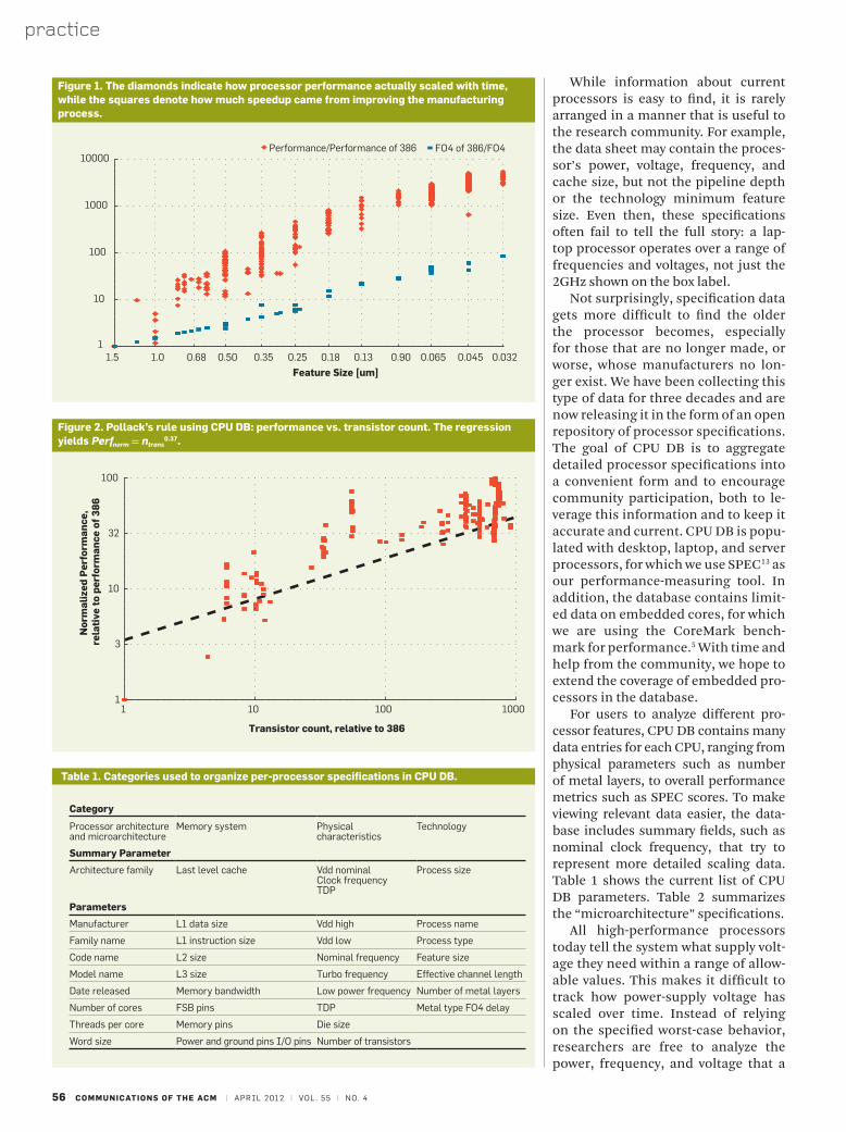
figure 1. the diamonds indicate how processor performance actually scaled with time, while the squares denote how much speedup came from improving the manufacturing process.
0.0320.0450.0650.900.130.180.250.350.500.681.01.51
10
100
1000
10000
Feature Size [um]
Performance/Performance of 386 FO4 of 386/FO4
figure 2. Pollack’s rule using cPu DB: performance vs. transistor count. the regression yields Perfnorm = ntrans
0.37.
1 10 100 10001
3
10
32
100
Transistor count, relative to 386
Nor
mal
ized
Per
form
ance
, re
lati
ve t
o p
erfo
rman
ce o
f 3
86
table 1. categories used to organize per-processor specifications in cPu DB.
category
processor architecture and microarchitecture
Memory system physical characteristics
technology
Summary Parameter
architecture family last level cache vdd nominal Clock frequency tdp
process size
Parameters
Manufacturer l1 data size vdd high process name
Family name l1 instruction size vdd low process type
Code name l2 size nominal frequency Feature size
Model name l3 size turbo frequency effective channel length
date released Memory bandwidth low power frequency number of metal layers
number of cores FsB pins tdp Metal type Fo4 delay
threads per core Memory pins die size
Word size power and ground pins i/o pins number of transistors

practice
april 2012 | vol. 55 | no. 4 | communicationS of the acm 57
processor actually uses while running an application, and then add it to the CPU DB repository. Table 3 is a sum-mary of the measured parameters tracked in CPU DB.
While CPU DB includes a large set of processor data fields, certain members of the architecture community will likely want to explore data fields that we did not think to include. To handle such situations, users are encouraged to suggest new data columns. These suggestions will be reviewed and then entered in the database.
A similar system helps keep CPU DB accurate and up to date. Users can submit data for new processors and architectures, and suggest corrections to data entries. We understand that users may not have data for all of the specifications, and we encourage us-ers to submit any subsets of the data fields. New data and corrections will be reviewed before being applied to the database.
With these mechanisms for adding and vetting data, CPU DB will be a pow-erful tool for architects who wish to incorporate processor data into their studies. Because many database users will probably want to perform analyses on the raw CPU DB data, the full data-base is downloadable in comma-sepa-rated value format.
technology normalization methodologyCPU DB allows side-by-side access to performance data for relatively simple in-order processors (up to the mid-1990s) and modern out-of-order pro-cessors. One could ask if, at the cost of lower performance, the simplic-ity of the older designs conferred an efficiency advantage. Unfortunately, direct comparisons using the raw data are difficult because, over the years, manufacturing technologies have im-proved significantly. A fair comparison would be possible if both processors were manufactured using the same process; but since porting all of these older processors to modern technolo-gies is not feasible, we need another approach. To enable such compari-sons, we instead estimate how pro-cessor performance and power would scale with technology.
Our main performance metric is based on industry-standard SPEC
CPU2006 scores.13 Unfortunately, most older processors did not run SPEC 2006 and instead measured performance in MIPS (million instructions per second) and, later, in terms of SPEC 1989, SPEC 1992, SPEC 1995, and SPEC 2000. In those cases we estimate SPEC 2006 numbers by converting old scores into a SPEC 2006 equivalent score using a conversion factor. The conversion val-ues are determined by examining sys-
tems that have scores for two versions of SPEC and then taking the geometric mean of the set of ratios between over-lapping scores. This method was used to create the summary performance scores in the database. We also provide the raw scores so that users can develop better conversion methods over time.
To estimate the performance of a processor if it were manufactured us-ing a newer process, we calculate the
figure 3. Pollack’s rule using cPu DB: performance vs. normalized area. the regression yields Perfnorm = ntrans
0.46.
1 10 100 10001
3
10
32
100
Normalized Core Area, relative to area of 386
Nor
mal
ized
Per
form
ance
, re
lati
ve t
o p
erfo
rman
ce o
f 3
86
table 2. microarchitectural parameters contained in cPu DB.
manufacturer microarchitecture Revision iSa
isa version isa extensions Floating point pipe stages
integer pipe stages
Max uops issued per cycle
integer functional units
load store functional units
Floating point functional units
total functional units
Max instructions decoded per cycle
reorder buffer instruction window size
instruction fetch queue size
Branch history table
Branch target buffer
Branch predictor accuracy
integer registers Floating point registers total registers Floating point coproc.
tlB entries out of order integrated mem. controller
table 3. measured parameters in cPu DB. note that spec benchmarks also include comprehensive fields for performance on individual SPec subtests.
Power voltage Performance
power for specified load idle power Max operating power
vdd for specified load vdd idle vdd at max power
speCrate 2006 speC 2006 speC 2000 speC 1995 speC 1992Mips

58 communicationS of the acm | april 2012 | vol. 55 | no. 4
practice
clock frequency in that technology us-ing gate-delay data. While the speed of the cache memory on the processor scales with technology, the delay go-ing to main memory has scaled only slowly with time. As a result, doubling the clock frequency generally does not double the processor’s performance. We finesse this issue the same way the microprocessor industry does: by scaling the on-chip cache so the per-centage memory stall time remains constant. Using the empirical rule that miss rates are proportional to the square root of the cache size,9,14
we expand the last-level cache by four times for each doubling of clock fre-quency. Thus, we assume that the pro-cessor performance scales with clock frequency, but we penalize the energy and area of the processor by growing its cache.
For the clock-cycle time estimate, we need to know how the delays of the gates and wires will scale. Fortu-nately, the delay scaling of different logic gates is similar, so it is sufficient to measure how the delay of a single gate scales. Our analysis uses the delay of an inverter driving four equivalent
inverters (a fanout of four, or FO4) as the gate-speed metric. Inverters are the most common gate type, and their delay is often published in technology papers. For wire delay it is important to remember that a design’s area will shrink with scaling, so its wire delay will, in general, reduce slowly or, at worst, stay constant. Its effect on cycle time depends on the internal circuit design. Designers generally pipeline long wires, so they tend not to limit the critical path. Thus, we ignore wire de-lay and make the slightly optimistic as-sumption that a processor’s frequency in the new technology will be greater by the ratio of FO4s from old to new:
f2 = f1FO41
FO42
Using FO4 as a basic metric has an additional advantage: it cleanly cov-ers the performance/energy variation that comes from changing the supply voltage. Two processors, even built in the same technology, might be oper-ated at different supply voltages. The energy difference between the two can be calculated directly from the supply voltage, but the voltage’s effect on per-formance is harder to estimate. Using FO4 data for these designs at two dif-ferent voltages provides all the infor-mation that is needed.
Having accounted for the effect of the scaled memory systems, we find that estimating the power of a pro-cessor with scaled technology is fairly straightforward. Processor power has two components: dynamic and leak-age. In an optimized design, the leak-age power is around 30% of the dynam-ic power, and the leakage power will scale as the dynamic power scales.16
Dynamic power is given by the prod-uct of the processor’s average activity factor, α (the probability that a node will switch each cycle), the processor frequency, and the energy to switch the transistors:
Energy = C{Vdd}2
The processor’s average activity fac-tor depends on the logic and not the technology, so it is constant with scal-ing. Since capacitance per unit length is roughly constant with scaling, C should be proportional to the feature size λ. We have already estimated how
figure 4. Scaling of transistor feature sizes over time. up to the 130nm node, feature size scaled every two to three years. Since the 90nm generation, feature size scaling has accelerated to every two years.
1985 1990 1995 2000 2005 2010 2015
32 nm
45 nm
65 nm
90 nm
0.13 um
0.18 um
0.25 um
0.35 um
0.50 um
0.68 um
1.0 um
1.5 um
IntelIBM
AMDOther
figure 5. in modern chips, the number of features per transistor has started to grow.
1985 1990 1995 2000 2005 2010
10
32
100
316
1000Features Per Transistor

practice
april 2012 | vol. 55 | no. 4 | communicationS of the acm 59
the frequency will scale, so the esti-mated power and performance scaling for technology is:
P2 = P1λ2V 2
dd2FO41
λ1V 2dd1 FO42
+ Pcache
Perf2 = Perf1
FO41
FO42
For analyzing processor efficiency, it is often better to look at energy per operation rather than power. Energy/op factors out the linear relationship that both performance and power have with frequency (FO4). Lowering the fre-quency changes the power but does not change the energy/op. Since energy/op is proportional to the ratio of power to performance, we derive equation 3 by dividing equations 1 and 2:
energyop
∝ P1
Perf1
λ2V 2dd2
λ1V 2dd1
+ Pcache
Perf1
FO42
FO41
With these expressions, it is pos-sible to normalize CPU DB proces-sors’ performance and energy into a single process technology. While In-tel’s Shekhar Borkar et al. gave a rough sketch of how technology scaling and architectural improvement contrib-uted to processor performance over the years,2 our data and normalization method can be used to generate an actual scatter plot showing the break-down between the two factors: faster transistors (resulting from technology scaling) and architectural improve-ment. As seen in Figure 1, process scaling and microarchitectural scal-ing each contribute nearly the same amount to processor performance gains.
As a quick sanity check for our nor-malization results, we plot normalized performance versus transistor count and normalized area in figures 2 and 3. These plots look at Pollack’s rule, which states that performance scales as the square root of design complexity.1 Pol-lack’s rule has been used in numerous published studies to compare perfor-mance against processor die resource usage.2,4,10,15 Figures 2 and 3 show that our normalized data is in close agree-ment with Pollack’s rule, suggesting our normalization method accurately represents design performance.
Physical ScalingOne of the nice side benefits of collect-ing this database is that it allows one to
see how chip complexity, voltage, and power have scaled over time, and how well scaling predictions compare with reality. The rate of feature scaling has accelerated in recent years (Figure 4). Up through the 130nm (nanometer) process generation, feature size scaled down by a factor of
α = 12
approximately every two to three years. Since the 90nm generation, however, a new process has been introduced approximately every two years. In-tel appears to be driving this intense schedule and has been one of the first to market for each process since the 180nm generation.
As a result of this exponential scal-ing, in the 25 years since the release of the Intel 80386, transistor area has
shrunk by a factor of almost 4,000. If feature size scaling were all that were driving processor density, then tran-sistor counts would have scaled by the same rate. An analysis of commercial microprocessors, however, shows that transistor count has actually grown by a factor of 16,000.
One simple reason why transistor growth has outpaced feature size is that processor dies have grown. While the 80386 microprocessor had a die size of 103 mm2, modern Intel Core i7 dies have an area of up to 296 mm2. This is not the whole story behind tran-sistor scaling, however. Figure 5 shows technology-independent transistor density by plotting how many square minimum features an average proces-sor transistor occupies. We generated this data by taking the die area, divid-
figure 6. voltage vs. feature size. it is clear that voltage scaling did not follow one simple rule. first, by convention, it was maintained at 5 volts. once voltage reductions were re-quired, a new convention was established at 3.3 volts. then voltage was reduced in propor-tion to feature size until the 130nm node. log-space regression reveals that voltage scaled roughly as the square root of feature size between the 0.6um and 130nm nodes.
slope = 0.63
10
5
3
2
1.5
1
2.37 0.56
Feature Size [um]
V dd
0.13 0.03
figure 7. Processor frequency scaling with time. as illustrated, processor frequency has largely leveled off since 2005.
1985 1990 1995 2000 2005 2010
10
32
100
316
1000
3162
10000Clock Frequency vs. Time
MH
z
IntelAMD
IBMDEC
SunOther

60 communicationS of the acm | april 2012 | vol. 55 | no. 4
practice
ing by the feature size squared, and then dividing by the number of tran-sistors. From 1985 to 2005 increasing metal layers and larger cache struc-tures (with their high transistor den-sities) had decreased the average size of a transistor by four times. Interest-ingly, since 2005, transistor density actually dropped by roughly a factor of two. While our data does not indicate a reason for this change, we suspect it results from a combination of stricter design rules for sub-wavelength lithog-raphy, using more robust logic styles in the processor, and a shrinking per-centage of the processor area used for cache in chip multiprocessors.
Our data also provides some inter-esting insight into how supply voltag-es have scaled over time. Most people
know voltage scales with technology feature size, so many assume that this scaling is proportional to feature size as originally proposed in Robert Den-nard’s 1974 article.6 As he and others have noted, however, and as shown in Figure 6, voltage has not scaled at the same pace as feature size.3,12 Until roughly the 0.6 µm node, processors maintained an operating voltage of 5 volts, since that was the common sup-ply voltage for popular logic families of the day, and processor power dis-sipation was not an issue. It was not until manufacturers went to 3.3 volts in the 0.6 µm generation that voltage began to scale with feature size. Fit-ting a curve on the voltage data from the half-micron to the 0.13 µm pro-cess generations, our data indicates
that, even when voltage scaled, it did so with roughly the square root of fea-ture size. This slower scaling has been attributed to reaping a dual benefit of faster gates and better immunity to noise and process variations at the cost of higher chip-power density.
From the 0.13 µm generation on, voltage scaling seems to have slowed. At the same time, however, trends in voltage have become much more dif-ficult to estimate from our data. As mentioned earlier, today almost all processors define their own operat-ing voltage. The data sheets have only the operating range. Figure 6 plots the maximum specified voltage. More user data should provide insight on how supply voltages are really scaling.
circuits and PipeliningCircuit designers and microarchitects were not content to scale frequency with gate speed—if they had been, then microprocessors would be running at only around 500MHz today. As Figure 7 shows, frequencies scaled much faster than simple gate speed. The reason for this discrepancy is largely because of architectural decisions that decreased the logic depth in each processor pipe-line stage and increased the number of stages. From 1985 to around 2000, the frequency rapidly increased as a result of faster, more parallel circuit imple-mentations of adders, branch units, and caches, and the use of aggressive pipelining. These trends are evident in the contrast between the two-stage fetch/execute pipeline of the Intel 80386, and the 30-plus pipeline stages in the Prescott Pentium IV.
Since 2000, processor frequencies have stagnated, but this is not the whole story. Our data confirms that gate speeds have continued to improve with technology. What is different now, though, is that the industry has moved away from deeply pipelined machines and is now designing machines that do more work per pipeline stage. The rea-son for this change is simple: power. While short-tick machines are possible and might be optimal from a perfor-mance perspective,7,11,14 they are not energy efficient.8
In light of slower voltage scaling and faster frequency scaling, it comes as no surprise that processor power has increased over time. As illustrated in
figure 8. Power density over time. from 1985 through 2005, power density grew by roughly a factor of 32. Since 2005, power density has largely started to decrease.
1985 1990 1995 2000 2005 2010
10
20
40
6080
100
200
400
600800
1000
2000Power Density
mW
/mm
2
figure 9. how power should have scaled, given how voltage, number of transistors, and performance actually scaled.
1985 1990 1995 2000 2005 20101
2
468
10
20
406080
100
200
400600800
1000
Wat
ts
Actual Power Projected Power

practice
april 2012 | vol. 55 | no. 4 | communicationS of the acm 61
Figure 8, processor power density has increased by more than a factor of 32 from the release of the 80386 through 2005, although it has recently started to decrease as energy-efficient comput-ing has grown in importance.
Interestingly, scaling rules say power should be much worse. From the Intel 80386 to a Pentium 4, feature size scaled by 16 times, supply volt-age scaled by around four times, and frequency scaled by 200 times. This means that the power density should have increased by a factor of 16 · 200/42 = 200, which is much larger than the power density increase of 32 times shown in Figure 8. Figure 9 compares observed power with how power should have scaled if we just scaled up an Intel 386 architecture to match the perfor-mance of new processors. The eight-fold savings represents circuit and mi-croarchitectural optimizations—such as clock gating—that have been done during this period to keep power under control. The energy savings of these techniques had initially been grow-ing, but, unfortunately, recently seems to have stabilized at around the eight-fold mark. This is not a good sign if we hope to continue to scale performance, since technology scaling of energy is slowing down.
microarchitecture and SoftwareWhile process technologists were finding ways to scale transistors, pro-cessor architects were working equally hard in advancing and innovating at the microarchitecture level. Indeed, this effect can be seen in CPU DB where, after normalizing for technology, we observe a hundredfold improvement in microarchitecture/software perfor-mance since the Intel 80386 days. His-torically, as the number of transistors per chip increased with technology scaling, architects found ways to use those transistors to create faster, more advanced uniprocessors. In addition to aggressive clock scaling, architects implemented features such as specula-tive execution, parallel instruction is-sue, out-of-order processing, and larger caches—all of which contributed to im-proved single-threaded performance.
By approximately 2005, increas-ingly complex processors, along with slowed voltage scaling, caused proces-sors to hit a new constraint: the power
wall. This resulted in a significant shift in the industry. Moore’s Law meant that processor designers could still expect an ever-increasing number of transistors, but they had to use these transistors in energy-efficient ways; increasing performance now meant decreasing energy/instruction to keep power constant. As a response to this challenge, the industry transitioned toward CMP (chip multiprocessor) de-signs that use many simple processors to increase the aggregate performance of the chip.
Figure 10 plots the technology-nor-malized energy/op versus the normal-ized performance. For this plot, we assume the power needed to scale up
the cache size is small compared with the processor power, providing an op-timistic assumption of the efficiency of these early machines. This plot indi-cates that, for early processor designs, energy/op remains relatively constant while performance scales up.
We noticed from this plot, howev-er, that some of the early processors (for example, the Pentium) appear far more energy efficient than mod-ern processor designs. To estimate the scaled energy of these processors more fairly, we scale the caches by the square of the improvement in frequen-cy to keep the memory stall percentage constant, and we estimate the power of a 45nm low-power SRAM at around
figure 10. energy/op vs. performance. note these energy/ops do not reflect any scaling of the on-chip memory system.
0.3 0.7 2.1 6 17.3 501x
2x
4x
8x
16x
32x
64x
SPEC int 2006
Rel
ativ
e en
erg
y/op
1990
1995
2000
2005
2010
85−90 90−95 95−00 00−05 05−11 Moving Average
figure 11. energy/op vs. performance, modified to scale up the memory system of older cores.
0.3 0.7 2.1 6 17.3 501x
2x
4x
8x
16x
32x
64x
SPEC int 2006
Rel
ativ
e en
erg
y/op
1990
1995
2000
2005
2010
85−90 90−95 95−00 00−05 05−11 Moving Average

62 communicationS of the acm | april 2012 | vol. 55 | no. 4
practice
0.5W/MB. Including this cache energy-correction factor yields the results in Figure 11. Comparing these two plots demonstrates how critical the memory system is for low-energy processors. The leakage power of our estimated large on-chip cache increases the en-ergy cost of an instruction by four to eight times for simple processors.
Surprisingly, however, the original Pentium designs are still substantially more energy efficient than other de-signs in the plot. Clearly, more analysis is warranted to understand whether this apparent efficiency can be lever-aged in future machines.
In recent years, desktop processors have shifted toward high-throughput parallel machines. With this shift, it was unclear whether processor de-signers would be able to scale single-core performance. A brief analysis of the data in Figure 12 shows that single-core performance continues to scale with each new architecture. Within an architecture, performance depends largely on the part’s frequen-cy and cache size. Figure 13 illustrates this point by plotting the performance versus frequency and cache size for several modern processor designs. Frequency scaling with each new ar-chitecture is slower than before, and peak frequencies are now often used only when the other processor cores are idle. Figure 14 plots cycle time measured in gate delays and shows why processor clock frequency seems to have stalled: processors moved to shorter pipelines, and the resulting slower frequency has taken some time to catch up to the older hyperpipe-lined rates.
More interesting is that even when controlling for the effects of frequency and cache size, single-core microarchi-tectural performance is still being im-proved with each generation of chips (Figure 13). Improvements such as on-chip memory controllers and extra execution units all play a role in deter-mining overall system efficiency, and architects are still finding improve-ments to make.
Our results, however, come with the caveat that some portion of the performance improvement in modern single-core performance comes from compiler optimizations. Figure 15 shows how performance of the SPEC
figure 12. Performance vs. year since 2005.
2005 2006 2007 2008 2009 2010 20110
5
10
15
20
25
30
35
40
SP
EC
int
20
06
Netburst Core Nehalem K8 K10 Power
figure 13. Performance vs. clock rate and cache size since 2005 (llc is the last level cache size).
Netburst Core Nehalem K8 K10 Power
0 0.5 1 1.5 2 2.5 3 3.5 40
5
10
15
20
25
30
35
Clock Rate [GHz]
SP
EC
int
20
06
2 MB
4 MB
6 MB
8 MB
figure 14. fo4 delays per cycle for processor designs. fo4 delay per cycle is roughly proportional to the amount of computation completed per cycle.
1985 1990 1995 2000 2005 20100
20406080
100120140
FO
4/c
ycle
figure 15. libquantum score vs. SPec score. this figure shows how compiler optimizations have led to performance boosts in libquantum.
libquantum overall SPEC
2008 2009 2010 2011 201216
32
64
128
256
512
1024
SP
EC
20
06

practice
april 2012 | vol. 55 | no. 4 | communicationS of the acm 63
even when controlling for the effects of frequency and cache size, single-core microarchitectural performance is still being improved with each generation of chips.
2006 benchmark Libquantum scales over time on the Intel Bloomfield ar-chitecture. Libquantum concentrates a large amount of computation in an inner for loop that can be optimized. As a result, Libquantum scores have risen 18 times without any improve-ment to the underlying hardware. Also, many SPEC scores for modern proces-sors are measured with the Auto Paral-lel flag turned on, indicating that the measured “single-core” performance might still be benefiting from multi-core computing.
conclusionOver the past 40 years, VLSI design-ers have used an incredible amount of engineering expertise to create and improve these amazing devices we call microprocessors. As a result, perfor-mance has improved and the energy/op has decreased by many orders of magnitude, making these devices the engines that power our information technology infrastructure. CPU DB is designed to help explore this area. Us-ing the data in CPU DB and some sim-ple scaling rules, we have conducted some preliminary studies to show the kinds of analyses that are possible. We encourage readers to explore and con-tribute to the processor data in CPU DB, and we look forward to learning more about processors from the in-sights they develop.
acknowledgmentsContributing authors to this article are: Omid Azizi, Hicamp Systems, Inc.; John S. Brunhaver II, Stanford Univer-sity; Ron Ho, Oracle; Stephen Rich-ardson, Stanford University; Ofer Sha-cham, Stanford University; and Alex Solomatnikov, Hicamp Systems, Inc.
For more information about the on-line CPU database and how to contribute data, please visit cpudb.stanford.edu.
Related articles on queue.acm.org
A Conversation with Steve Furber
http://queue.acm.org/detail.cfm?id=1716385
Real-World Concurrency
Bryan Cantrill, Jeff Bonwickhttp://queue.acm.org/detail.cfm?id=1454462
The Price of Performance Luiz André Barrosohttp://queue.acm.org/detail.cfm?id=1095420
References1. borkar, s. thousand core chips: a technology
perspective. in Proceedings of the 44th annual Design Automation Conference (2007), 746–749; http://doi.acm.org/10.1145/1278480.1278667.
2. borkar, s. and chien, a.a. the future of microprocessors. Commun. ACM 54, 5 (may 2011), 67–77; http://doi.acm.org/10.1145/1941487.1941507.
3. chang, l., Frank, D., montoye, r., Koester, s., Ji, b., coteus, P., Dennard, r. and haensch, w. Practical strategies for power-efficient computing technologies. in Proceedings of the IEEE 98, 2 (2010); 215–236.
4. chung, e.s., milder, P.a., hoe, J.c. and mai, K. single-chip heterogeneous computing: Does the future include custom logic, FPgas, and gPgPus? in Proceedings of the 43rd Annual IEEE/ACM International Symposium on Microarchitecture (2010), 225–236; http://dx.doi.org/10.1109/micro.2010.36.
5. coremark, an eembc benchmark. coremark scores for embedded and desktop cPus; http://www.coremark.org/home.php.
6. Dennard, r., gaensslen, F., yu, h., rideout, V., bassous, e. and leblanc, a. Design of ion-implanted mosFets with very small physical dimensions. in Proceedings of the IEEE 87, 4 (1999), 668–678 (reprinted from ieee Journal of solid-state circuits, 1974).
7. hartstein, a. and Puzak, t. the optimum pipeline depth for a microprocessor. in Proceedings of the 29th Annual International Symposium on Computer Architecture (2002), 7–13.
8. hartstein, a. and Puzak, t. optimum power/performance pipeline depth. in Proceedings of the 36th Annual IEEE/ACM International Symposium on Microarchitecture (Dec. 2003), 117–125.
9. hartstein, a., srinivasan, V., Puzak, t.r. and emma, P.g. cache miss behavior: is it √2? in Proceedings of the 3rd Conference on Computing Frontiers (2006), 313–320; http://doi.acm.org/10.1145/1128022.1128064.
10. hill, m. and marty, m. amdahl’s law in the multicore era. Computer 41, 7 (2008), 33–38.
11. hrishikesh, m., Jouppi, n., Farkas, K., burger, D., Keckler, s. and shivakumar, P. the optimal logic depth per pipeline stage is 6 to 8 Fo4 inverter delays. in Proceedings of the 29th Annual International Symposium on Computer Architecture (2002), 14–24.
12. nowak, e.J. maintaining the benefits of cmos scaling when scaling bogs down. IBM Journal of Research and Development 46, 2.3 (2002), 169–180.
13. standard Performance evaluation corporation (sPec). sPec cPu2006 results; http://www.spec.org/cpu2006/results/.
14. sprangle, e., carmean, D. increasing processor performance by implementing deeper pipelines. in Proceedings of the 29th Annual International Symposium on Computer Architecture (2002), 25–34.
15. woo, D.h. and lee, h.-h. extending amdahl’s law for energy-efficient computing in the many-core era. Computer 41, 12 (2008), 24–31.
16. Zhang, x. high-performance low-leakage design using power compiler and multi-Vt libraries. synopsys users group (snug) europe, 2003.
Andrew Danowitz is currently a Ph.D. candidate in electrical engineering at stanford university. his research focuses on reconfigurable hardware design methodologies and energy efficient architectures.
Kyle Kelley is a Ph.D candidate in electrical engineering at stanford university. his research interests include energy-efficient Vlsi design and parallel computing.
James Mao is a Ph.D. candidate in the Vlsi research group at stanford university working on verification tools for mixed-signal designs.
John P. Stevenson is a graduate of the u.s. naval academy and served as an officer onboard the uss Los Angeles (ssn-688) prior to entering the Ph.D. program at stanford university. his interests include computer architecture and digital circuit design. he is investigating novel memory-system architectures.
Mark horowitz is chair of the electrical engineering department and the yahoo! Founders Professor at stanford university, and a founder of rambus, inc. his research interests span using ee and cs analysis methods to problems in molecular biology to creating new design methodologies for analog and digital Vlsi circuits.
© 2012 acm 0001-0782/12/04 $10.00