CPE 335 Computer Organization Basic MIPS...
29
CPE 335 Computer Organization Basic MIPS Architecture – Part I Dr. Iyad Jafar Adapted from Dr. Gheith Abandah slides http://www.abandah.com/gheith/Courses/CPE335_S08/index.html 1
-
Upload
phungxuyen -
Category
Documents
-
view
221 -
download
1
Transcript of CPE 335 Computer Organization Basic MIPS...
CPE 335Computer Organization
Basic MIPS Architecture – Part I
Dr. Iyad Jafar
Adapted from Dr. Gheith Abandah slides
http://www.abandah.com/gheith/Courses/CPE335_S08/index.html
CPE232 Basic MIPS Architecture 1
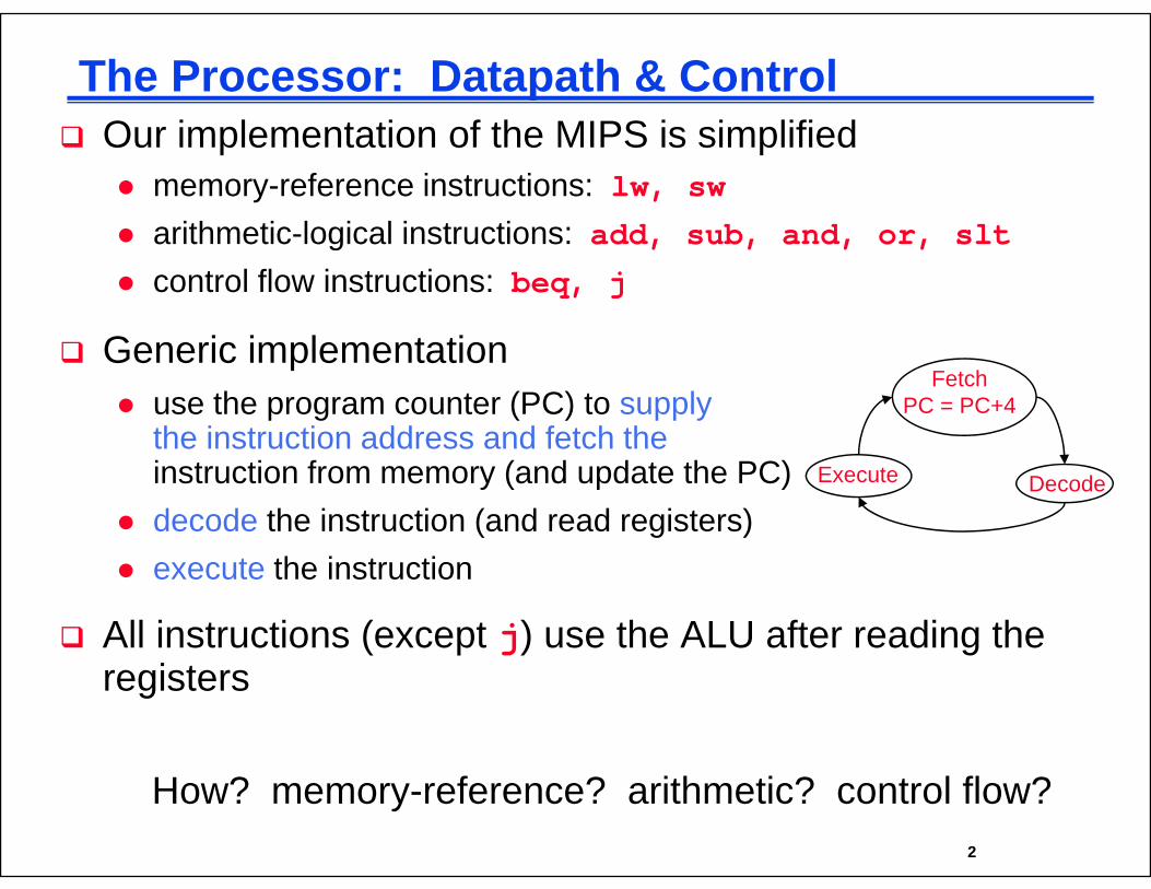
O i l t ti f th MIPS i i lifi dThe Processor: Datapath & Control
Our implementation of the MIPS is simplifiedmemory-reference instructions: lw, swarithmetic logical instructions: dd b d ltarithmetic-logical instructions: add, sub, and, or, sltcontrol flow instructions: beq, j
G i i l t tiGeneric implementationuse the program counter (PC) to supply the instruction address and fetch the
FetchPC = PC+4
the instruction address and fetch the instruction from memory (and update the PC)decode the instruction (and read registers)
DecodeExecute
execute the instruction
All instructions (except j) use the ALU after reading the registers
CPE232 Basic MIPS Architecture 2
How? memory-reference? arithmetic? control flow?
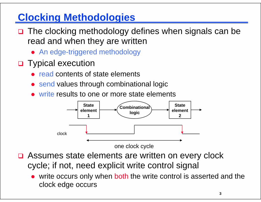
Clocking MethodologiesThe clocking methodology defines when signals can be read and when they are written
An edge triggered methodologyAn edge-triggered methodologyTypical execution
read contents of state elements send values through combinational logicwrite results to one or more state elements
Stateelement
1
Stateelement
2
Combinationallogic
clock
one clock cycle
Assumes state elements are written on every clock cycle; if not, need explicit write control signal
it l h b th th it t l i t d d th
CPE232 Basic MIPS Architecture 3
write occurs only when both the write control is asserted and the clock edge occurs
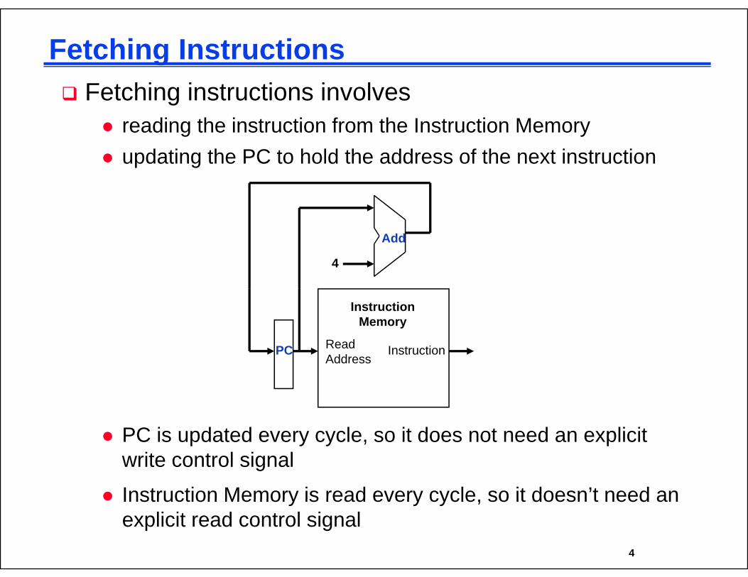
Fetching InstructionsFetching instructions involves
reading the instruction from the Instruction MemoryC fupdating the PC to hold the address of the next instruction
Add
4
ReadAddress
Instruction
InstructionMemory
PCAddress
PC i d t d l it d t d li itPC is updated every cycle, so it does not need an explicit write control signal
Instruction Memory is read every cycle so it doesn’t need an
CPE232 Basic MIPS Architecture 4
Instruction Memory is read every cycle, so it doesn t need an explicit read control signal
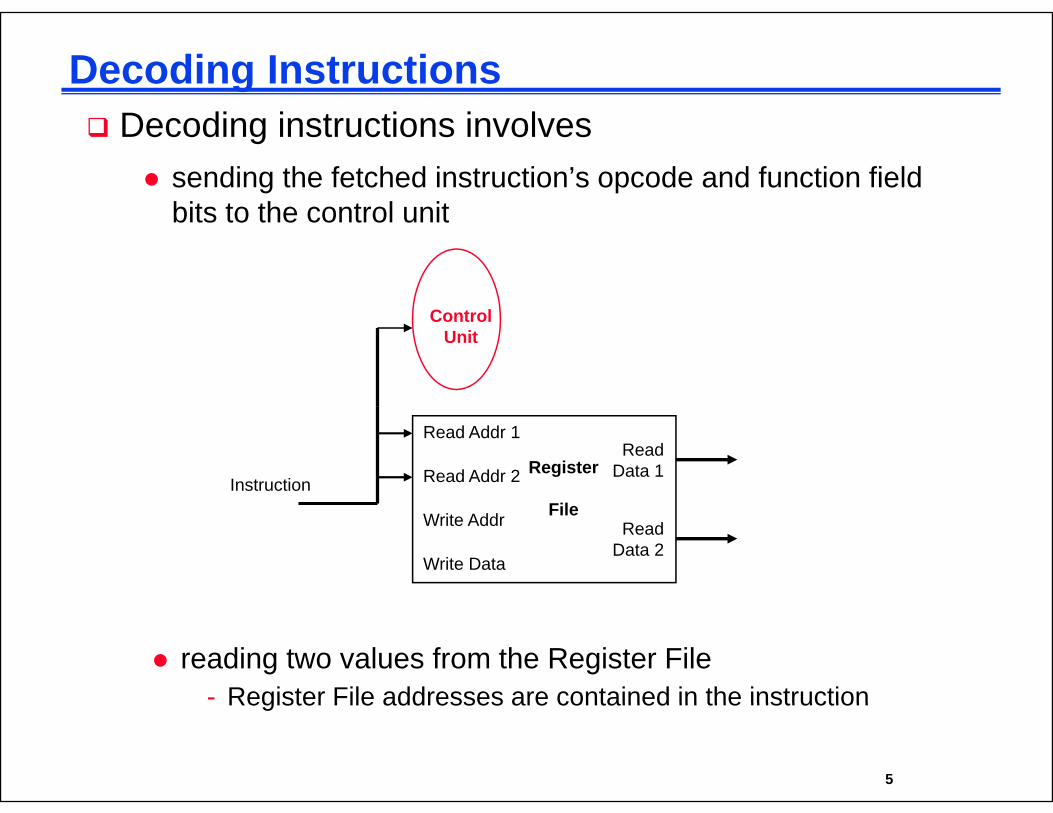
Decoding InstructionsDecoding instructions involves
sending the fetched instruction’s opcode and function field bits to the control unitbits to the control unit
ControlUnit
Instruction
Read Addr 1
Read Addr 2 Register
Fil
ReadData 1
Write Data
Write Addr FileRead
Data 2
reading two values from the Register File- Register File addresses are contained in the instruction
CPE232 Basic MIPS Architecture 5
Register File addresses are contained in the instruction
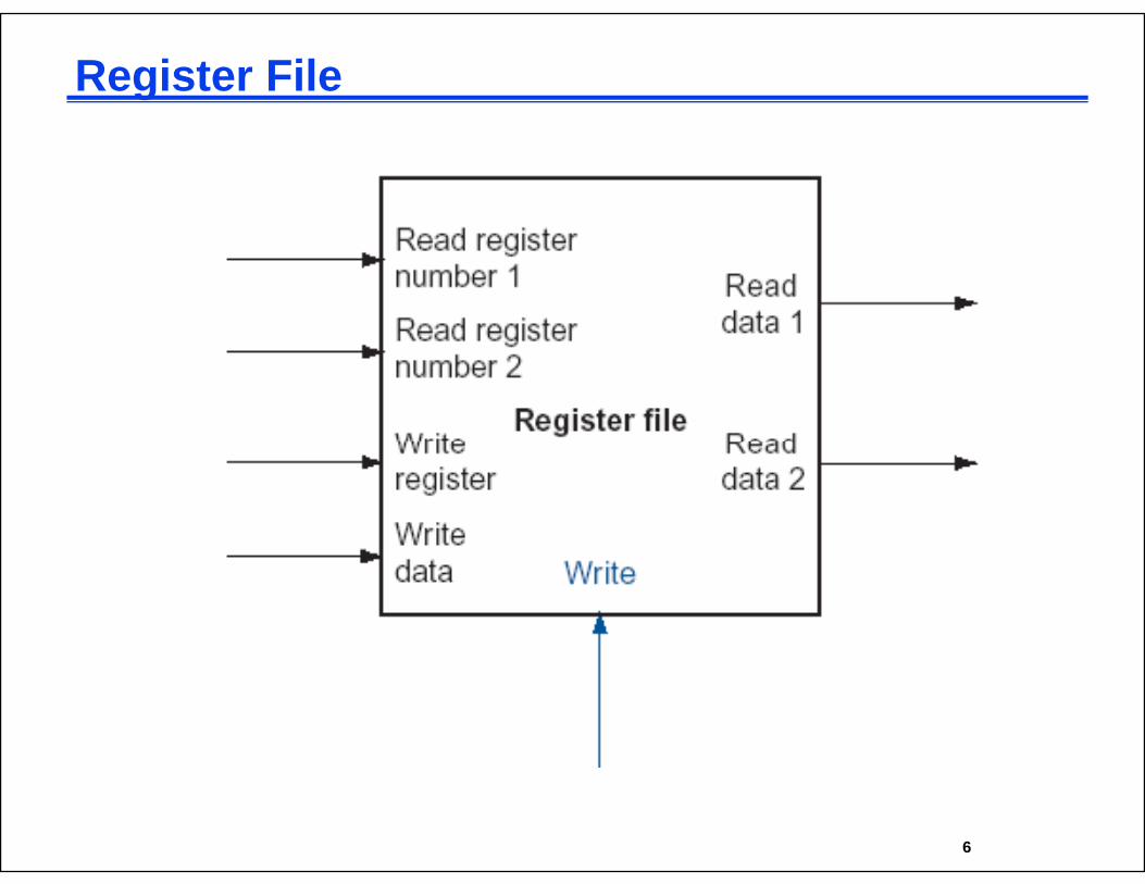
Register File
CPE232 Basic MIPS Architecture 6
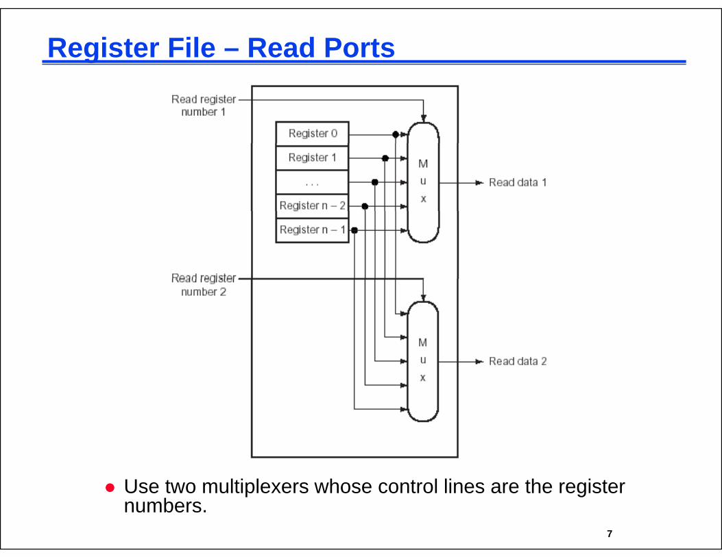
Register File – Read Ports
U t lti l h t l li th i t
CPE232 Basic MIPS Architecture 7
Use two multiplexers whose control lines are the register numbers.
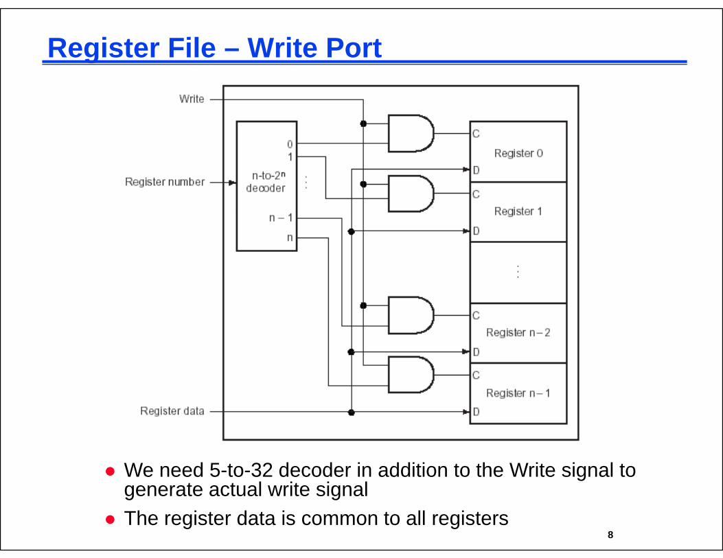
Register File – Write Port
We need 5-to-32 decoder in addition to the Write signal to t t l it i l
CPE232 Basic MIPS Architecture 8
generate actual write signal The register data is common to all registers
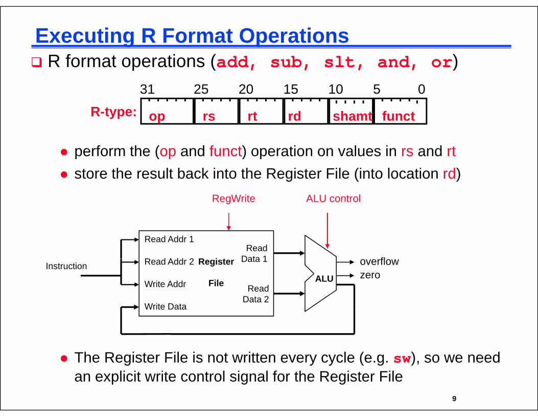
Executing R Format OperationsR f t ti ( dd b lt d )R format operations (add, sub, slt, and, or)
R t31 25 20 15 5 010
perform the (op and funct) operation on values in rs and rt
R-type: op rs rt rd functshamt
p ( p ) pstore the result back into the Register File (into location rd)
ALU controlRegWrite
Read Addr 1
R d Add 2 R i tRead
Data 1 flInstruction
Write Data
Read Addr 2
Write Addr
Register
File
Data 1
ReadData 2
ALU
overflowzero
Write Data
The Register File is not written every cycle (e g sw) so we need
CPE232 Basic MIPS Architecture 9
The Register File is not written every cycle (e.g. sw), so we need an explicit write control signal for the Register File
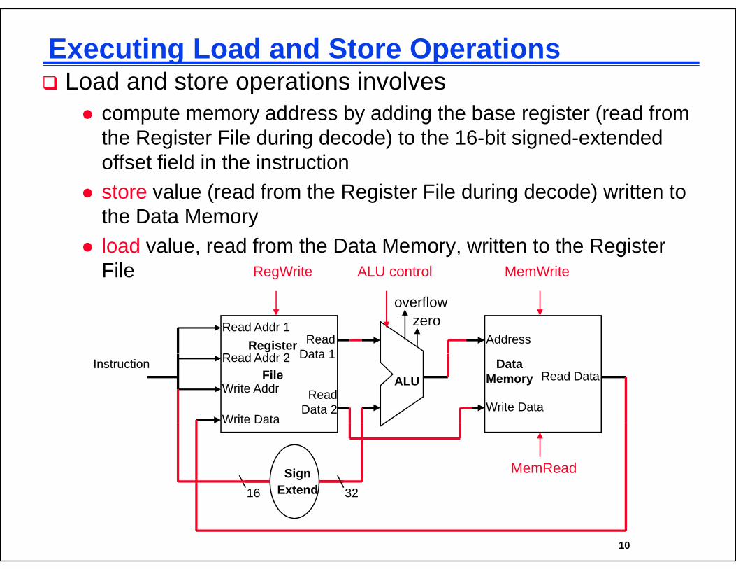
Executing Load and Store OperationsLoad and store operations involvesLoad and store operations involves
compute memory address by adding the base register (read from the Register File during decode) to the 16-bit signed-extended g g ) goffset field in the instructionstore value (read from the Register File during decode) written to the Data Memorythe Data Memoryload value, read from the Data Memory, written to the Register File ALU controlRegWrite MemWrite
Read Addr 1
R d Add 2Register Read
Data 1
overflowzero
Address
Instruction
Write Data
Read Addr 2
Write AddrFile
Data 1
ReadData 2
ALUData
Memory
Write Data
Read Data
Write Data
SignExtend
MemRead
16 32
CPE232 Basic MIPS Architecture 10
Extend16 32
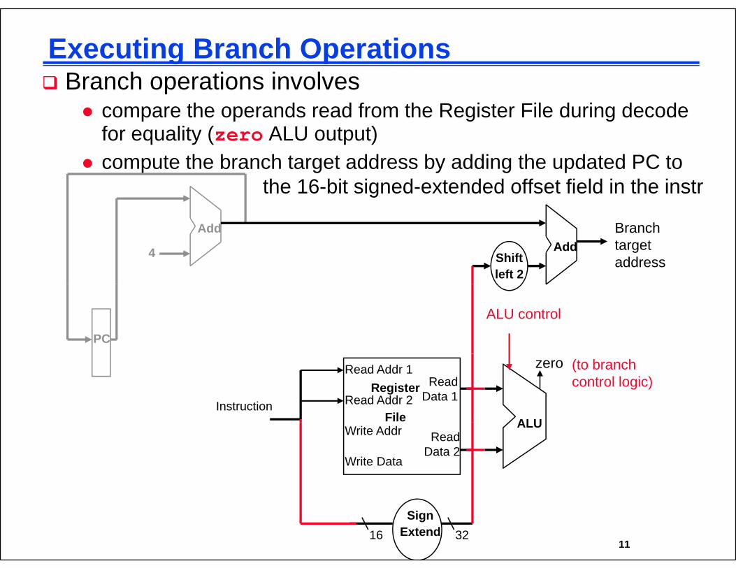
Executing Branch OperationsBranch operations involvesBranch operations involves
compare the operands read from the Register File during decode for equality (zero ALU output)compute the branch target address by adding the updated PC to
the 16-bit signed-extended offset field in the instr
Shiftleft 2
Add
4 AddBranchtargetaddress
ALU control
PC
Instruction
Read Addr 1
Read Addr 2Register
File
ReadData 1
ALU
zero (to branch control logic)
Write Data
Write Addr ReadData 2
ALU
CPE232 Basic MIPS Architecture 11
SignExtend16 32
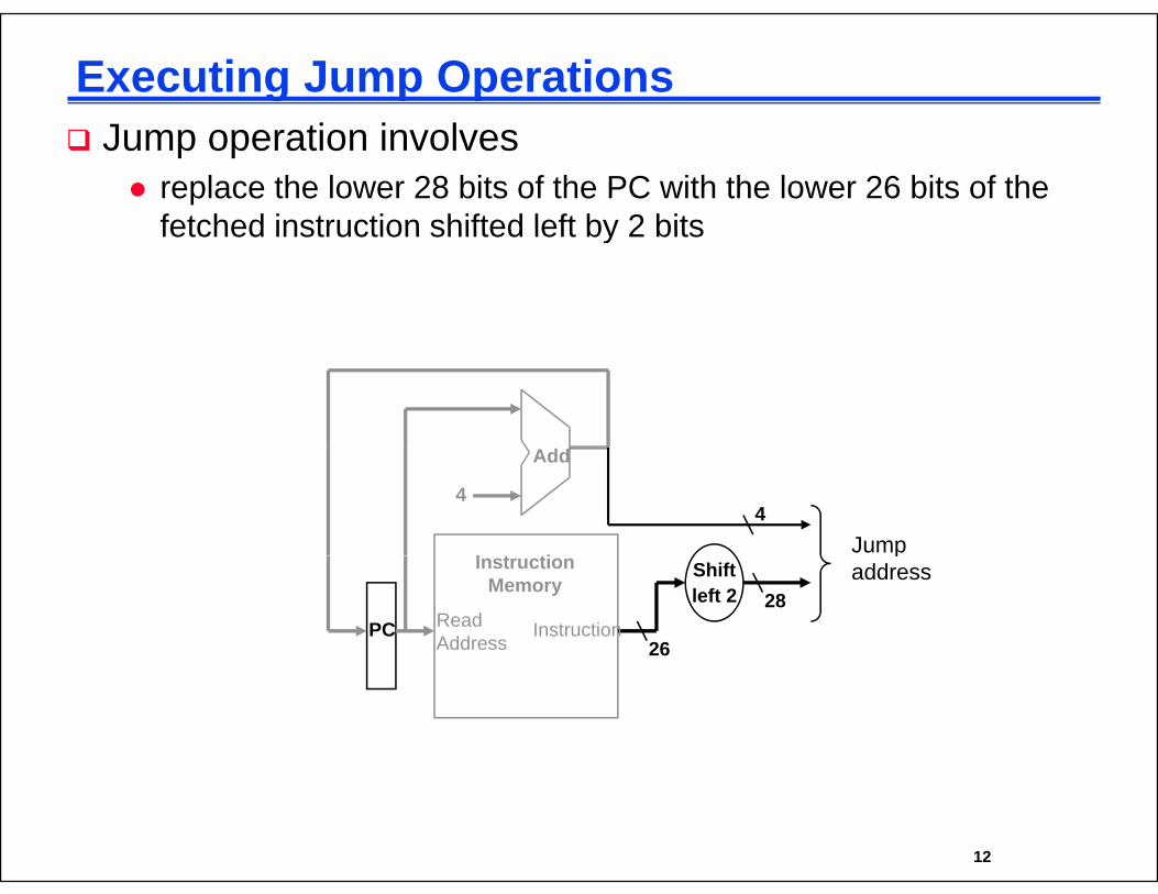
Executing Jump OperationsJump operation involves
replace the lower 28 bits of the PC with the lower 26 bits of the fetched instruction shifted left by 2 bitsfetched instruction shifted left by 2 bits
I t ti
Add
4
Jump4
ReadAddress
Instruction
InstructionMemory
PC
Shiftleft 2
paddress
26
28
CPE232 Basic MIPS Architecture 12
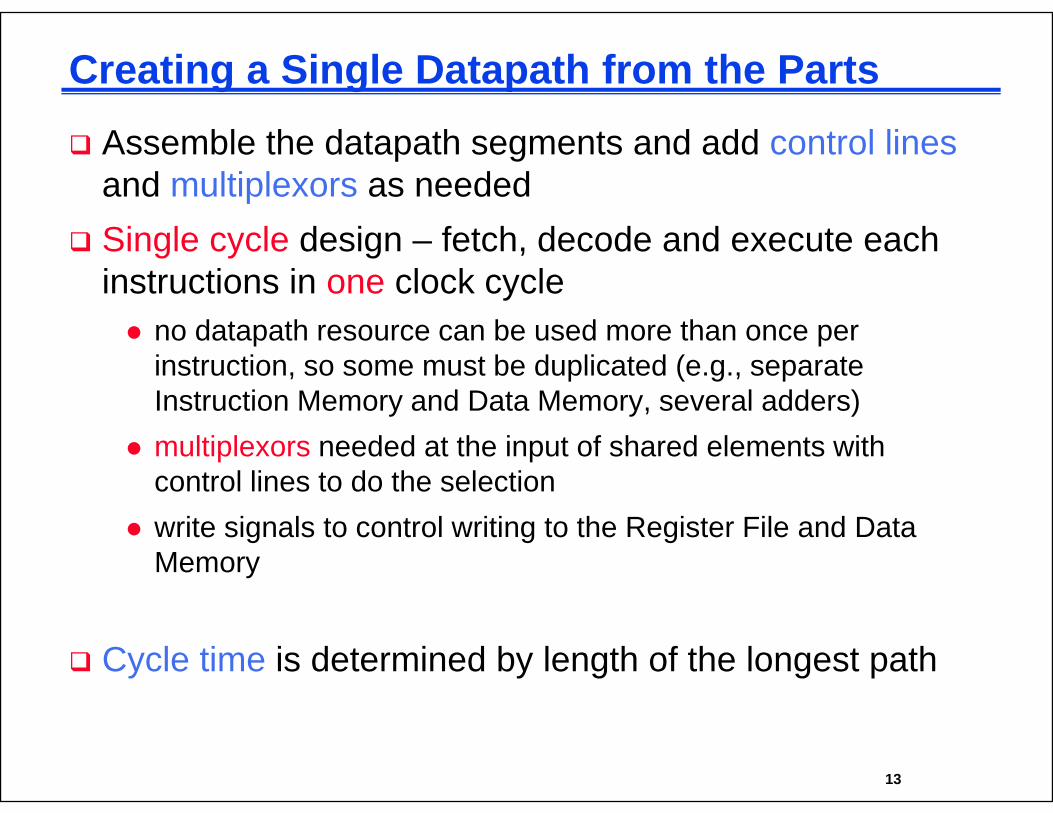
Creating a Single Datapath from the Parts
Assemble the datapath segments and add control lines and multiplexors as neededSingle cycle design – fetch, decode and execute each instructions in one clock cycle
no datapath resource can be used more than once per instruction, so some must be duplicated (e.g., separate Instruction Memory and Data Memory several adders)Instruction Memory and Data Memory, several adders)multiplexors needed at the input of shared elements with control lines to do the selectionwrite signals to control writing to the Register File and Data Memory
Cycle time is determined by length of the longest path
CPE232 Basic MIPS Architecture 13
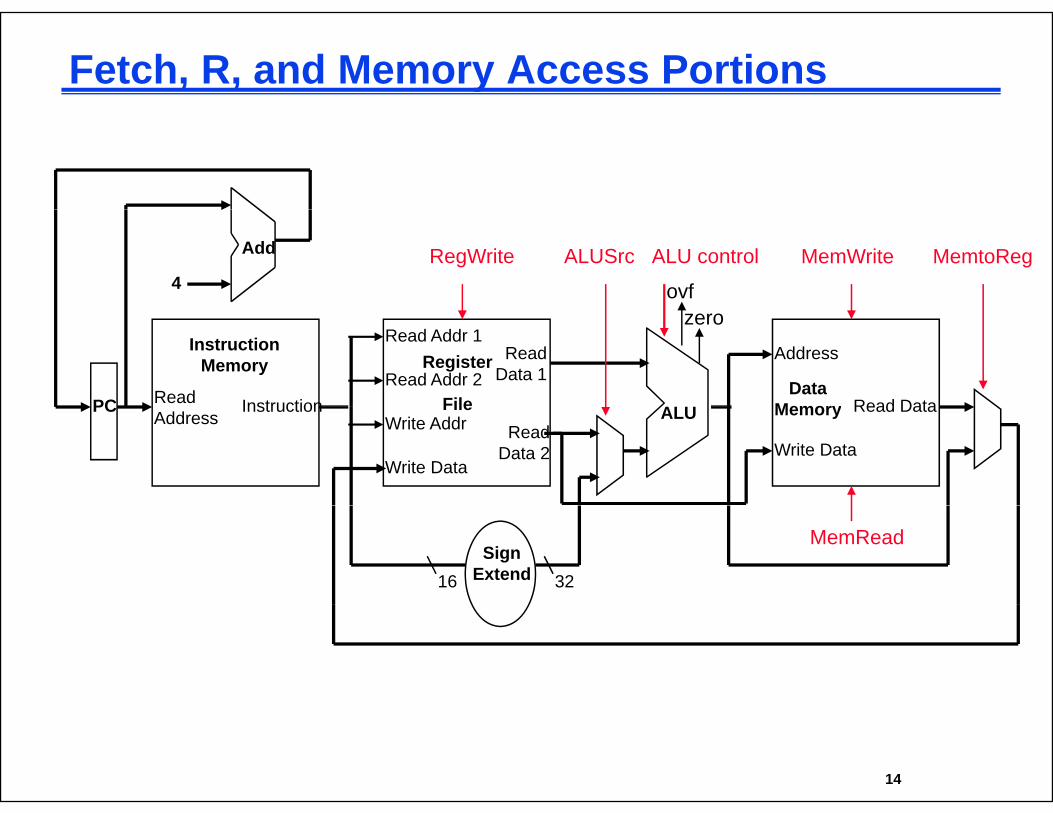
Fetch, R, and Memory Access Portions
MemtoRegAdd
4 ovf
ALU controlRegWrite MemWriteALUSrc
Read Instruction
InstructionMemory
PC
Read Addr 1
Read Addr 2Register
File
ReadData 1
ALU
zero
DataMemory
Address
Read DataAddress
InstructionPC
Write Data
Write AddrFile
ReadData 2
ALU Memory
Write Data
Read Data
MemReadSign
Extend16 32
CPE232 Basic MIPS Architecture 14
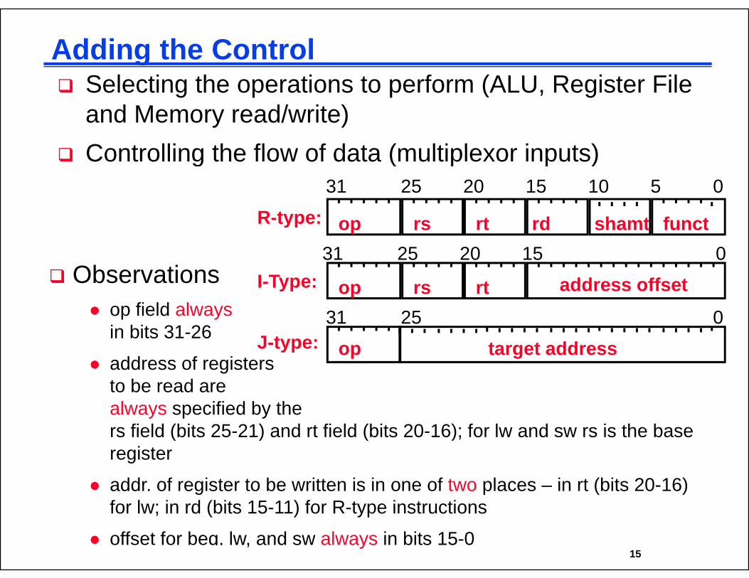
Adding the ControlS l ti th ti t f (ALU R i t FilSelecting the operations to perform (ALU, Register File and Memory read/write)Controlling the flow of data (multiplexor inputs)Controlling the flow of data (multiplexor inputs)
R-type:31 25 20 15 5 0
t d f th t
10
I-Type: op rs rt address offset31 25 20 15 0
R-type: op rs rt rd functshamt
Observations yp op rs rt address offsetop field alwaysin bits 31-26
dd f i tJ-type:
31 25 0
op target addressaddress of registers to be read are always specified by the rs field (bits 25 21) and rt field (bits 20 16); for lw and sw rs is the basers field (bits 25-21) and rt field (bits 20-16); for lw and sw rs is the base register
addr. of register to be written is in one of two places – in rt (bits 20-16)
CPE232 Basic MIPS Architecture 15
for lw; in rd (bits 15-11) for R-type instructions
offset for beq, lw, and sw always in bits 15-0
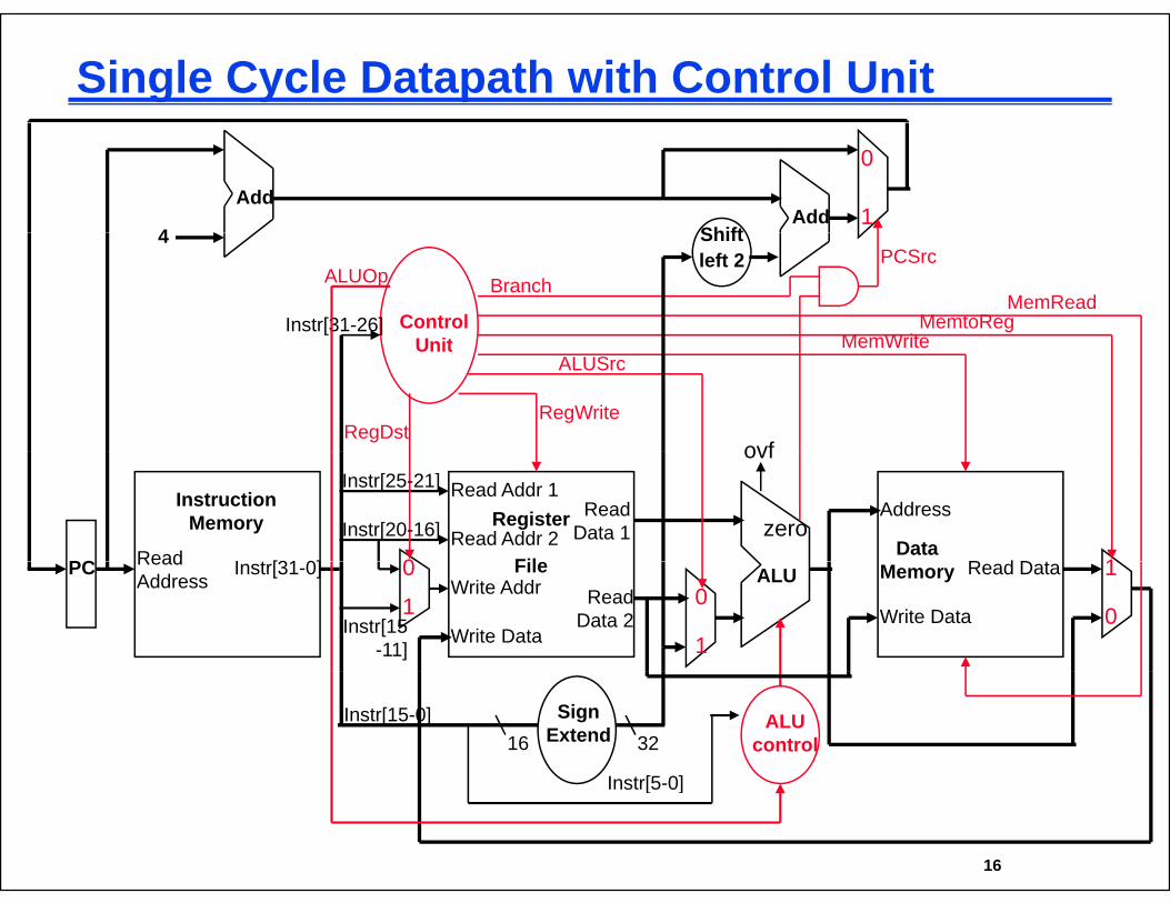
Single Cycle Datapath with Control Unit
Add
4 ShiftAdd
0
14
MemWrite
MemReadMemtoReg
Shiftleft 2 PCSrc
ALUOp
ControlUnit
Instr[31-26]
Branch
ovf
RegWrite
MemWriteALUSrc
RegDst
Unit
Read I t [31 0]
InstructionMemory
PC
Read Addr 1
Read Addr 2Register
Fil
ReadData 1
ovf
zeroData
Address
R d D t 10
Instr[25-21]
Instr[20-16]ReadAddress
Instr[31-0]PC
Write Data
Write AddrFile
ReadData 2
ALU Memory
Write Data
Read Data 1
1
1
00
0Instr[15 -11]
SignExtend16 32
ALUcontrol
Instr[5 0]
Instr[15-0]
CPE232 Basic MIPS Architecture 16
Instr[5-0]
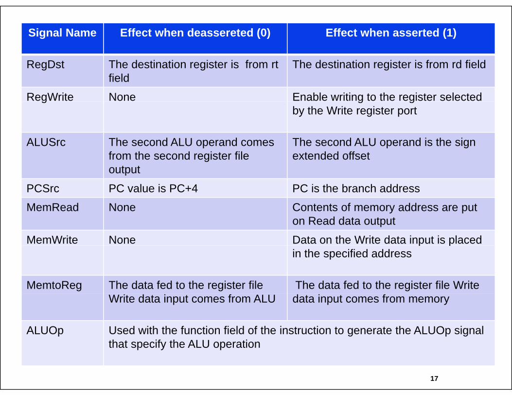
Single Cycle Datapath with Control UnitSignal Name Effect when deassereted (0) Effect when asserted (1)
RegDst The destination register is from rtfield
The destination register is from rd field
RegWrite None Enable writing to the register selected g g gby the Write register port
ALUSrc The second ALU operand comes The second ALU operand is the sign from the second register file output
extended offset
PCSrc PC value is PC+4 PC is the branch addressMemRead None Contents of memory address are put
on Read data output
MemWrite None Data on the Write data input is placed p pin the specified address
MemtoReg The data fed to the register file The data fed to the register file Write Write data input comes from ALU data input comes from memory
ALUOp Used with the function field of the instruction to generate the ALUOp signal th t if th ALU ti
CPE232 Basic MIPS Architecture 17
that specify the ALU operation
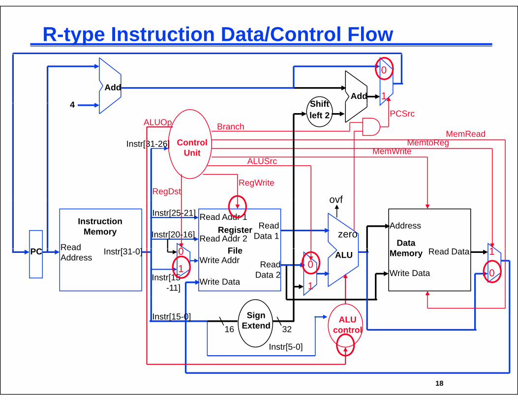
R-type Instruction Data/Control Flow
Add
4 ShiftAdd
0
14
MemWrite
MemReadMemtoReg
Shiftleft 2 PCSrc
ALUOp
ControlUnit
Instr[31-26]
Branch
ovf
RegWrite
MemWriteALUSrc
RegDst
Unit
Read I t [31 0]
InstructionMemory
PC
Read Addr 1
Read Addr 2Register
Fil
ReadData 1
ovf
zeroData
Address
R d D t 10
Instr[25-21]
Instr[20-16]ReadAddress
Instr[31-0]PC
Write Data
Write AddrFile
ReadData 2
ALU Memory
Write Data
Read Data 1
1
1
00
0Instr[15 -11]
SignExtend16 32
ALUcontrol
Instr[5 0]
Instr[15-0]
CPE232 Basic MIPS Architecture 18
Instr[5-0]
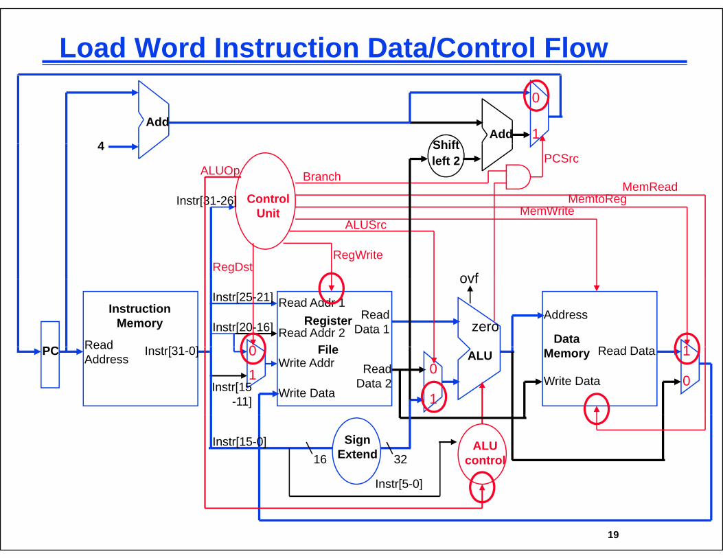
Load Word Instruction Data/Control Flow
Add
4 ShiftAdd
0
14
MemWrite
MemReadMemtoReg
Shiftleft 2 PCSrc
ALUOp
ControlUnit
Instr[31-26]
Branch
ovf
RegWrite
MemWriteALUSrc
RegDst
Unit
Read I t [31 0]
InstructionMemory
PC
Read Addr 1
Read Addr 2Register
Fil
ReadData 1
ovf
zeroData
Address
R d D t 10
Instr[25-21]
Instr[20-16]ReadAddress
Instr[31-0]PC
Write Data
Write AddrFile
ReadData 2
ALU Memory
Write Data
Read Data 1
1
1
00
0Instr[15 -11]
SignExtend16 32
ALUcontrol
Instr[5 0]
Instr[15-0]
CPE232 Basic MIPS Architecture 19
Instr[5-0]
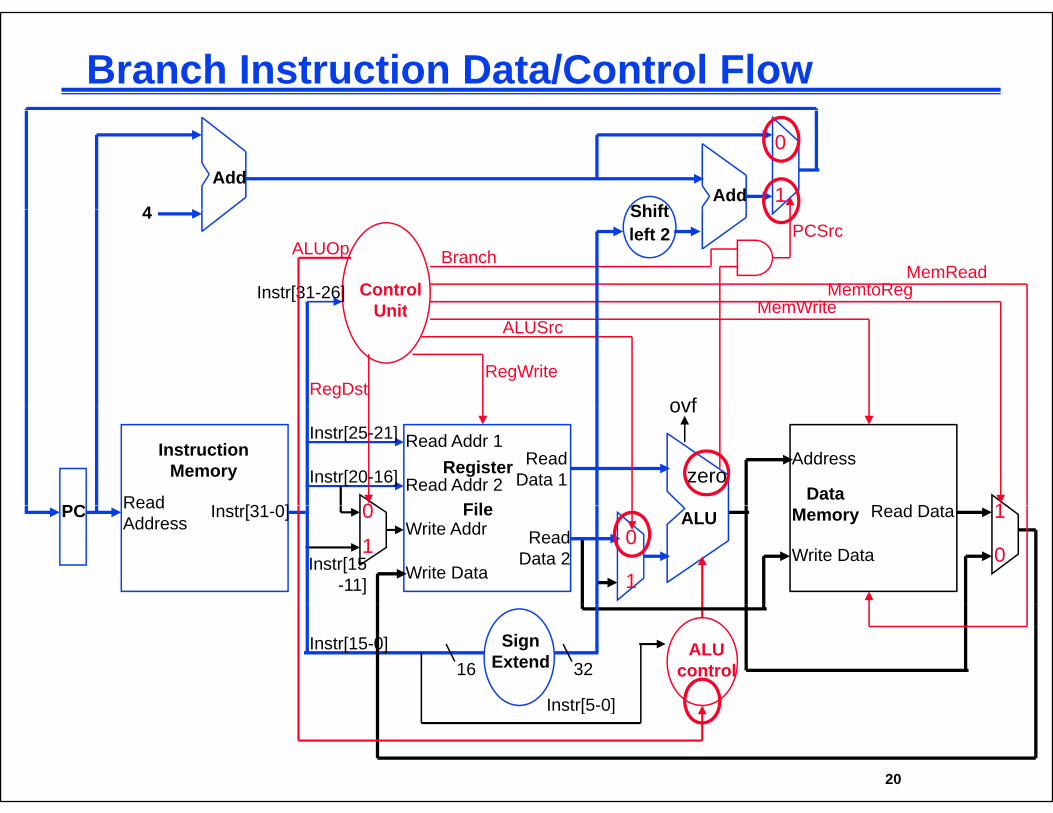
Branch Instruction Data/Control Flow
Add
4 ShiftAdd
0
14
MemWrite
MemReadMemtoReg
Shiftleft 2 PCSrc
ALUOp
ControlUnit
Instr[31-26]
Branch
ovf
RegWrite
MemWriteALUSrc
RegDst
Unit
Read I t [31 0]
InstructionMemory
PC
Read Addr 1
Read Addr 2Register
Fil
ReadData 1
ovf
zeroData
Address
R d D t 10
Instr[25-21]
Instr[20-16]ReadAddress
Instr[31-0]PC
Write Data
Write AddrFile
ReadData 2
ALU Memory
Write Data
Read Data 1
1
1
00
0Instr[15 -11]
SignExtend16 32
ALUcontrol
Instr[5 0]
Instr[15-0]
CPE232 Basic MIPS Architecture 20
Instr[5-0]
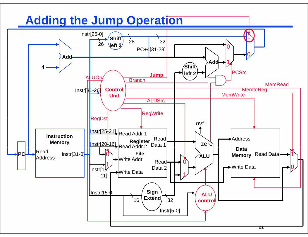
Adding the Jump Operation I t [25 0]
AddAdd
0
1
Shiftleft 2
0
132
Instr[25-0]
26PC+4[31-28]
28
4
MemReadMemtoReg
Shiftleft 2
Add
PCSrc
1
ALUOp
ControlInstr[31 26]
BranchJump
RegWrite
MemWriteMemtoReg
ALUSrc
RegDst
ControlUnit
Instr[31-26]
InstructionMemory
Read Addr 1
Read Addr 2Register Read
Data 1
ovf
zeroD t
Address
RegDst
Instr[25-21]
Instr[20-16]ReadAddress
Instr[31-0]PC
Write Data
Read Addr 2
Write AddrFile
ReadData 2
ALUData
Memory
Write Data
Read Data 1
1
1
00
0Instr[15 -11]
SignExtend16 32
ALUcontrol
1
Instr[15-0]
-11]
CPE232 Basic MIPS Architecture 21
Instr[5-0]
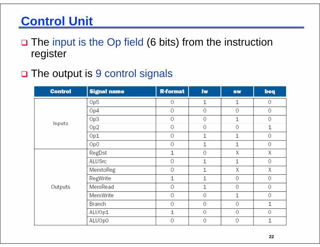
Control UnitThe input is the Op field (6 bits) from the instruction register
The output is 9 control signals
CPE232 Basic MIPS Architecture 22
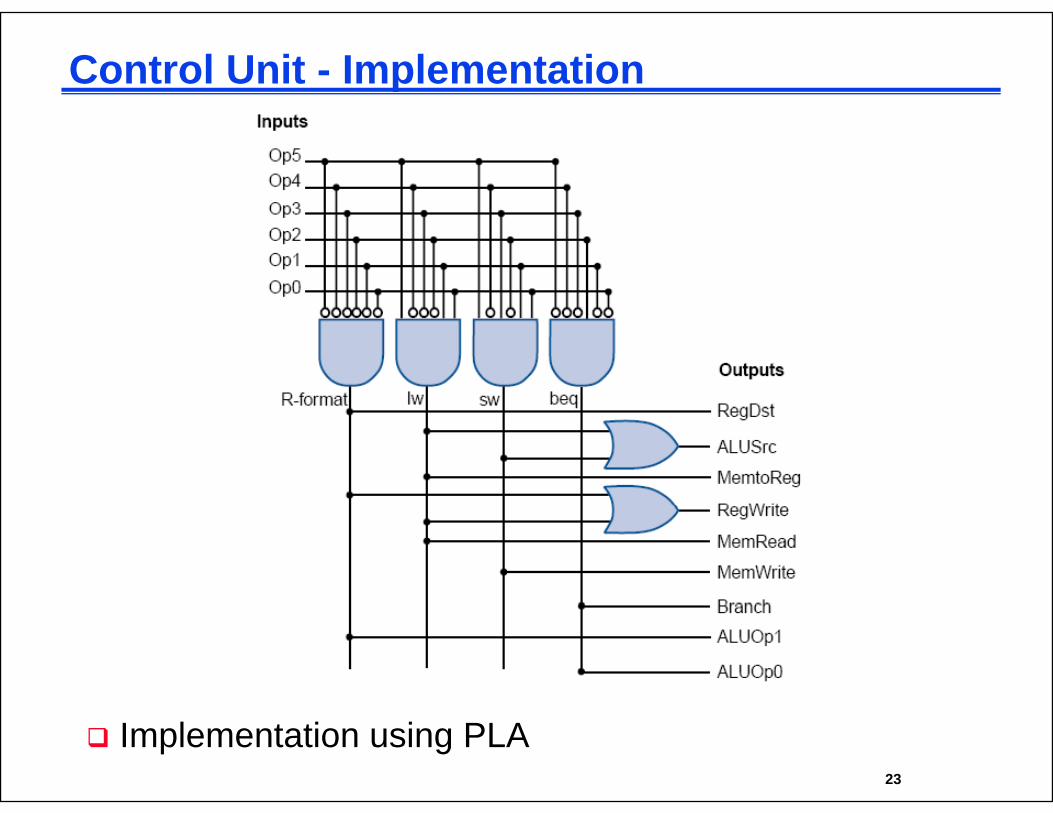
Control Unit - Implementation
CPE232 Basic MIPS Architecture 23
Implementation using PLA
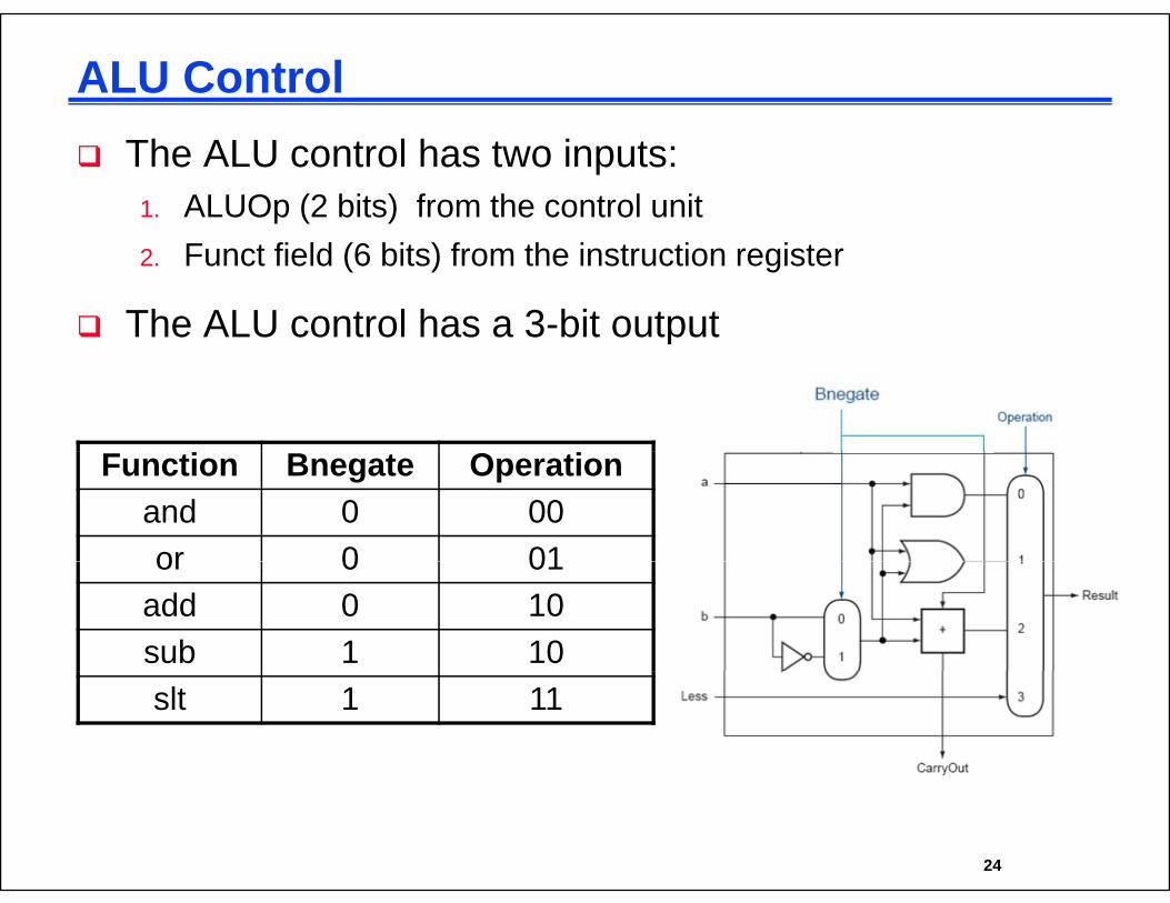
ALU ControlThe ALU control has two inputs:
1. ALUOp (2 bits) from the control unit2. Funct field (6 bits) from the instruction register
The ALU control has a 3-bit outputp
Function Bnegate Operationand 0 00or 0 01or 0 01
add 0 10sub 1 10slt 1 11
CPE232 Basic MIPS Architecture 24
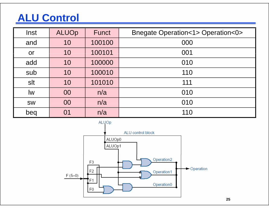
ALU ControlInst ALUOp Funct Bnegate Operation<1> Operation<0>and 10 100100 000or 10 100101 001or 10 100101 001
add 10 100000 010sub 10 100010 110slt 10 101010 111lw 00 n/a 010sw 00 n/a 010sw 00 n/a 010beq 01 n/a 110
CPE232 Basic MIPS Architecture 25
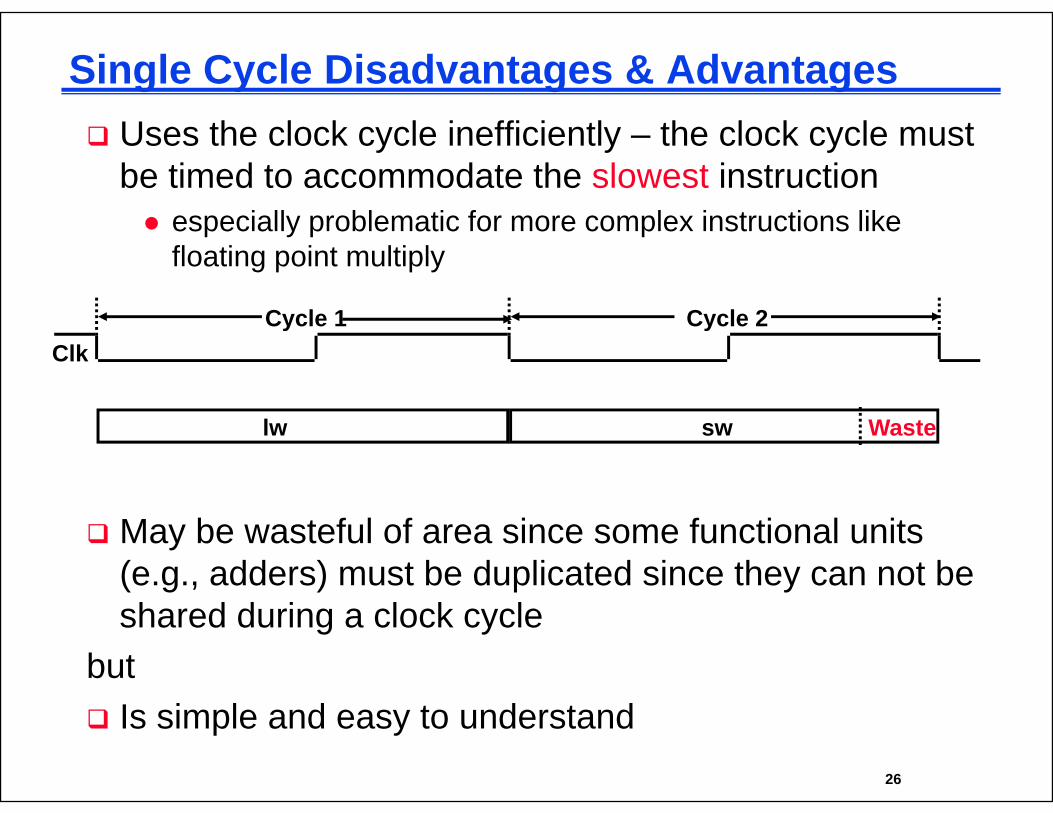
Single Cycle Disadvantages & AdvantagesUses the clock cycle inefficiently – the clock cycle must be timed to accommodate the slowest instruction
especially problematic for more complex instructions like floating point multiply
ClkCycle 1 Cycle 2
lw sw Waste
May be wasteful of area since some functional units (e.g., adders) must be duplicated since they can not be h d d i l k lshared during a clock cycle
but
CPE232 Basic MIPS Architecture 26
Is simple and easy to understand
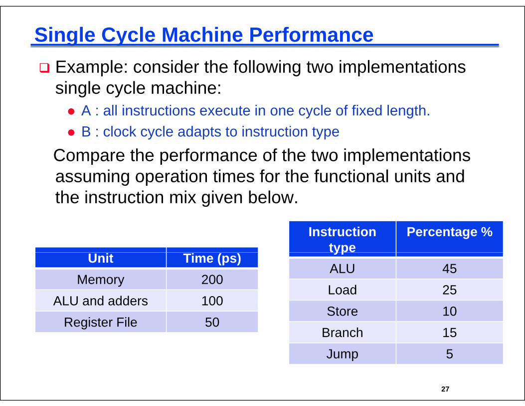
Single Cycle Machine PerformanceExample: consider the following two implementations single cycle machine:
A : all instructions execute in one cycle of fixed length. B : clock cycle adapts to instruction type
Compare the performance of the two implementationsCompare the performance of the two implementations assuming operation times for the functional units and the instruction mix given below.the instruction mix given below.
Instruction type
Percentage %
Unit Time (ps)Memory 200
ALU and adders 100
ypALU 45Load 25
ALU and adders 100Register File 50
Store 10Branch 15J 5
CPE232 Basic MIPS Architecture 27
Jump 5
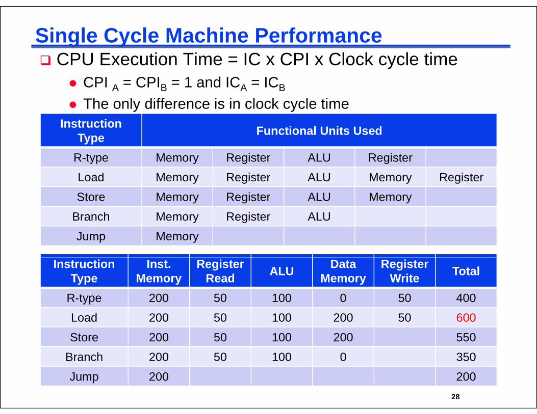
Single Cycle Machine PerformanceCPU Execution Time = IC x CPI x Clock cycle timeCPU Execution Time = IC x CPI x Clock cycle time
CPI A = CPIB = 1 and ICA = ICB
The only difference is in clock cycle timeThe only difference is in clock cycle timeInstruction
Type Functional Units Used
R type Memory Register ALU RegisterR-type Memory Register ALU RegisterLoad Memory Register ALU Memory RegisterStore Memory Register ALU Memory
Branch Memory Register ALUJump Memory
Instruction Type
Inst.Memory
Register Read ALU Data
MemoryRegister
Write Total
R-type 200 50 100 0 50 400Load 200 50 100 200 50 600Store 200 50 100 200 550
Branch 200 50 100 0 350
CPE232 Basic MIPS Architecture 28
Branch 200 50 100 0 350Jump 200 200
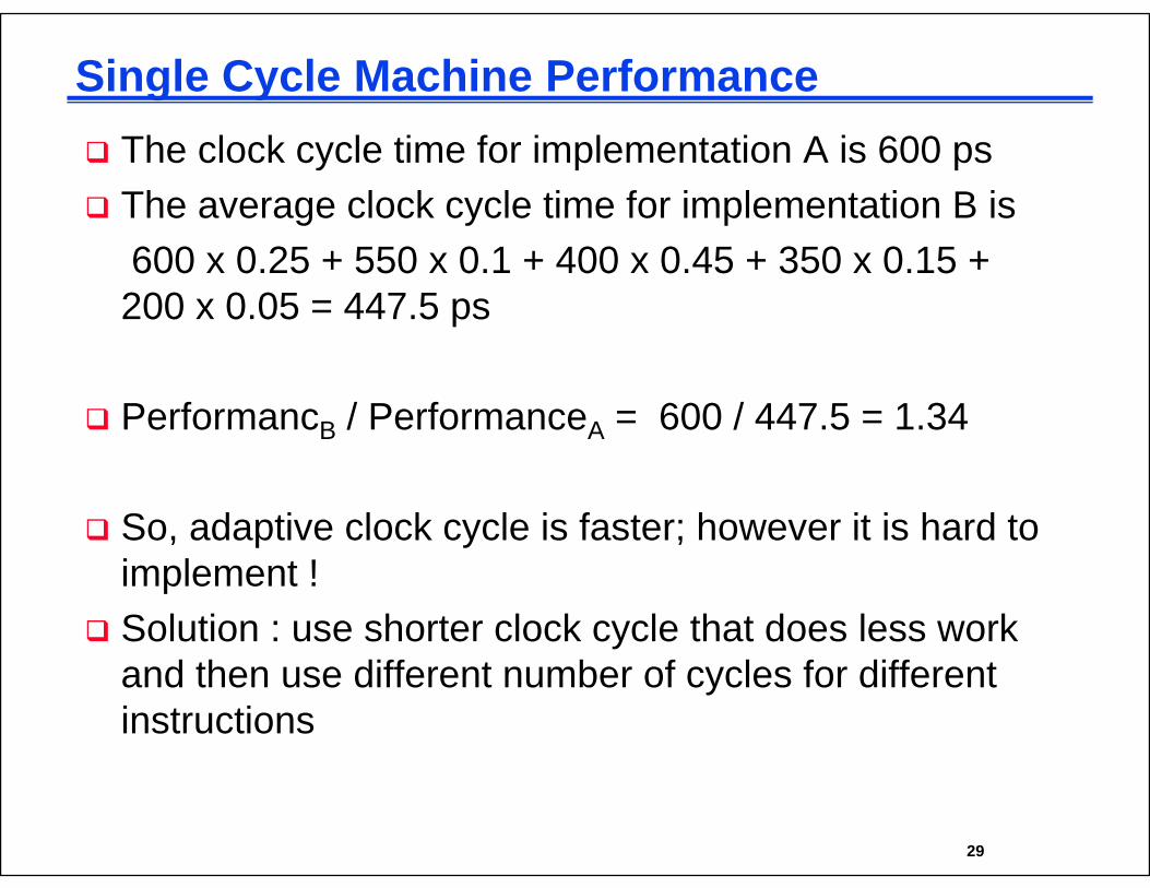
Single Cycle Machine PerformanceThe clock cycle time for implementation A is 600 psThe average clock cycle time for implementation B is 600 x 0.25 + 550 x 0.1 + 400 x 0.45 + 350 x 0.15 + 200 x 0.05 = 447.5 ps
PerformancB / PerformanceA = 600 / 447.5 = 1.34
So, adaptive clock cycle is faster; however it is hard to implement ! Solution : use shorter clock cycle that does less work
d h diff b f l f diffand then use different number of cycles for different instructions
CPE232 Basic MIPS Architecture 29


![CPE 335 Computer OrganizationComputer Organization Basic ... · CPE232 Basic MIPS Architecture 6 Instr[5-0] control. Multicycle Machine: 1-bit Control Signals Signal Effect when deasserted](https://static.fdocuments.us/doc/165x107/601ac1ef37dd2f2ed965d577/cpe-335-computer-organizationcomputer-organization-basic-cpe232-basic-mips-architecture.jpg)