CPE 323 Introduction to Embedded Computer Systems: Watchdog Timer, Timer A Instructor: Dr Aleksandar...
33
CPE 323 Introduction to Embedded Computer Systems: Watchdog Timer, Timer A Instructor: Dr Aleksandar Milenkovic Lecture Notes
-
Upload
bernice-park -
Category
Documents
-
view
229 -
download
0
Transcript of CPE 323 Introduction to Embedded Computer Systems: Watchdog Timer, Timer A Instructor: Dr Aleksandar...

CPE 323 Introduction to Embedded Computer Systems:Watchdog Timer, Timer A
Instructor: Dr Aleksandar MilenkovicLecture Notes

MSP430: Watchdog Timer

CPE 323 3
Watchdog Timer
GeneralThe primary function of the watchdog-timer module (WDT) is to perform a controlled-system restart after a software problem occurs. If the selected time interval expires, a system reset is generated. If the watchdog function is not needed in an application, the module can work as an interval timer, to generate an interrupt after the selected time interval.
Features of the Watchdog Timer include: Eight software-selectable time intervals Two operating modes: as watchdog or interval timer Expiration of the time interval in watchdog mode, which generates a system
reset; or in timer mode, which generates an interrupt request Safeguards which ensure that writing to the WDT control register is only
possible using a password Support of ultralow-power using the hold mode
Watchdog/Timer two functions: SW Watchdog Mode Interval Timer Mode

CPE 323 4
Watchdog Timer-Diagram

CPE 323 5
Watchdog Timer-Registers
Watchdog Timer CounterThe watchdog-timer counter (WDTCNT) is a 16-bit up-counter that is not directly accessible by software. The WDTCNT is controlled through the watchdog-timer control register (WDTCTL), which is a 16-bit read/write register located at the low byte of word address 0120h. Any read or write access must be done using word instructions with no suffix or .w suffix. In both operating modes (watchdog or timer), it is only possible to write to WDTCTL using the correct password.
Watchdog Timer Control Register
MDB, LowByte
Password Compare
MDB, HighByte R/W
EQU
WDT 16-bit Control Register with Write Protection
Read:HighByte is 069h Write:HighByte is 05Ah, otherwisesecurity key is violated
HOLD NMINMIES TMSEL CNTCL SSEL IS1
7 0
ISO
0120h WDTCTL
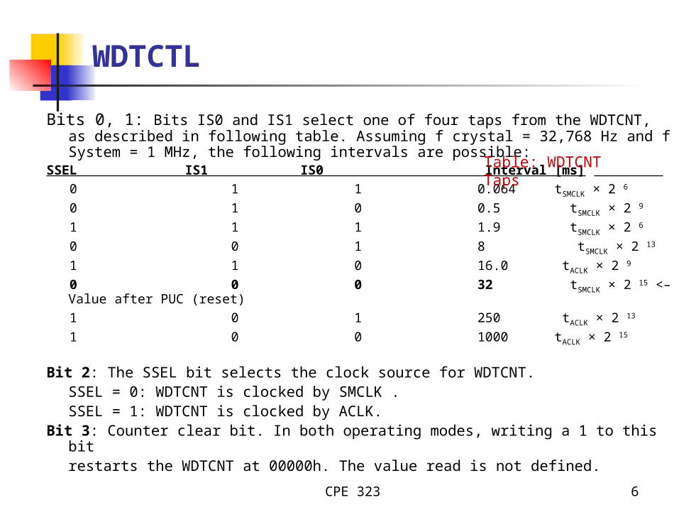
Bits 0, 1: Bits IS0 and IS1 select one of four taps from the WDTCNT, as described in following table. Assuming f crystal = 32,768 Hz and f System = 1 MHz, the following intervals are possible:
CPE 323 6
WDTCTL
Bits 0, 1: Bits IS0 and IS1 select one of four taps from the WDTCNT, as described in following table. Assuming f crystal = 32,768 Hz and f System = 1 MHz, the following intervals are possible:
SSEL IS1 IS0 Interval [ms]
0 1 1 0.064 tSMCLK × 2 6
0 1 0 0.5 tSMCLK × 2 9
1 1 1 1.9 tSMCLK × 2 6
0 0 1 8 tSMCLK × 2 13
1 1 0 16.0 tACLK × 2 9
0 0 0 32 tSMCLK × 2 15 <– Value after PUC (reset)
1 0 1 250 tACLK × 2 13
1 0 0 1000 tACLK × 2 15
Bit 2: The SSEL bit selects the clock source for WDTCNT.SSEL = 0: WDTCNT is clocked by SMCLK .SSEL = 1: WDTCNT is clocked by ACLK.
Bit 3: Counter clear bit. In both operating modes, writing a 1 to this bitrestarts the WDTCNT at 00000h. The value read is not defined.
Table: WDTCNT Taps

CPE 323 7
WDTCTL
Bit 4: The TMSEL bit selects the operating mode: watchdog or timer.TMSEL = 0: Watchdog modeTMSEL = 1: Interval-timer mode
Bit 5: The NMI bit selects the function of the RST/NMI input pin. It is cleared by the PUC signal.
NMI = 0: The RST/NMI input works as reset input.As long as the RST/NMI pin is held low, the internal signal is active (level sensitive).NMI = 1: The RST/NMI input works as an edge-sensitive non-maskable interrupt input.
Bit 6: If the NMI function is selected, this bit selects the activating edge of the RST/NMI input. It is cleared by the PUC signal.NMIES = 0: A rising edge triggers an NMI interrupt.NMIES = 1: A falling edge triggers an NMI interrupt.CAUTION: Changing the NMIES bit with software can generate an NMI interrupt.
Bit 7: This bit stops the operation of the watchdog counter. The clock multiplexer is disabled and the counter stops incrementing. It holds the last value until the hold bit is reset and the operation continues. It is cleared by the PUC signal.HOLD = 0: The WDT is fully active.HOLD = 1: The clock multiplexer and counter are stopped.

CPE 323 8
Watchdog Timer-Interrupt Function
The Watchdog Timer (WDT) uses two bits in the SFRs for interrupt control.
The WDT interrupt flag (WDTIFG) (located in IFG1.0, initial state is reset)
The WDT interrupt enable (WDTIE) (located in IE1.0, initial state is reset) When using the watchdog mode, the WDTIFG flag is used by the reset interrupt
service routine to determine if the watchdog caused the device to reset. If the flag is set, then the Watchdog Timer initiated the reset condition (either by timing out or by a security key violation). If the flag is cleared, then the PUC was caused by a different source. See chapter 3 for more details on the PUC and POR signals.
When using the Watchdog Timer in interval-timer mode, the WDTIFG flag is set after the selected time interval and a watchdog interval-timer interrupt is requested. The interrupt vector address in interval-timer mode is different from that in watchdog mode. In interval-timer mode, the WDTIFG flag is reset automatically when the interrupt is serviced.
The WDTIE bit is used to enable or disable the interrupt from the Watchdog Timer when it is being used in interval-timer mode. Also, the GIE bit enables or disables the interrupt from the Watchdog Timer when it is being used in interval-timer mode.
CPE 323 9
Watchdog Timer-Timer Mode
Setting WDTCTL register bit TMSEL to 1 selects the timer mode. This mode provides periodic interrupts at the selected time interval. A time interval can also be initiated by writing a 1 to bit CNTCL in the WDTCTL register.
When the WDT is configured to operate in timer mode, the WDTIFG flag is set after the selected time interval, and it requests a standard interrupt service. The WDT interrupt flag is a single-source interrupt flag and is automatically reset when it is serviced. The enable bit remains unchanged. In interval-timer mode, the WDT interrupt-enable bit and the GIE bit must be set to allow the WDT to request an interrupt. The interrupt vector address in timer mode is different from that in watchdog mode.

CPE 323 10
Watchdog Timer-Examples
How to select timer mode/* WDT is clocked by fACLK (assumed 32Khz) */
WDTCL=WDT_ADLY_250; // WDT 250MS/4 INTERVAL TIMER
IE1 |=WDTIE; // ENABLE WDT INTERRUPT
How to stop watchdog timer
WDTCTL=WDTPW + WDTHOLD ; // stop watchdog timer
Assembly programming
WDT_key .equ 05A00h ; Key to access WDTWDTStop mov #(WDT_Key+80h),&WDTCTL ; Hold WatchdogWDT250 mov #(WDT_Key+1Dh),&WDTCTL ; WDT, 250ms Interval

MSP430: Timer_A

CPE 323 12
Timer_A MSP430x1xx
Most-versatile, general-purpose timer in MSP430 Features
16-bit counter with 4 operating modes Selectable and configurable clock source Three (five, seven) independently configurable
capture/compare registers with configurable inputs Three (five, seven) individually configurable
output modules with 8 output modes Multiple, simultaneous, timings; multiple
capture/compares; multiple output waveforms such as PWM signals; and any combination of these.
Interrupt capabilities each capture/compare block individually configurable

CPE 323 13
Page 11-3, User’s Manual
Timer_A5 - MSP430x1xx Block Diagram
Timer Block
(TAR)
Capture & compare channels
(TACCRx)

CPE 323 14
TimerA Organization
Timer block (TAR) up/down counter with a choice of clock sources that can be
prescaled (divided) TAIFG is raised when the counter returns to 0
Capture & compare channel Capture: we capture an input, which means record the “time”
(value in TAR) at which the input changes in TACCRn; the input can be internal (from another peripheral or SW) or external
Compare: the current value of TAR is compared to the value stored in TACCRn and the output is updated when they match; the output can be either internal or external
Request an interrupt on either capture or compare or by setting its CCIFG flag (e.g., from SW)
Sample an input at a compare event; useful if TimerA is used for serial communication

CPE 323 15
TimerA Organization
Single Timer block, multiple Capture&Compare channels We may have multiple TimerA modules that can
operate on independent time bases Use HW (TimerA) for more precise timing and
reserve software for the less critical tasks TACCR0 is special
Used for UP and UP/DOWN mode and cannot be used for usual functions
Has its own interrupt vector with a higher priority than the other interrupts from TimerA, which all share a common vector
CPE 323 16
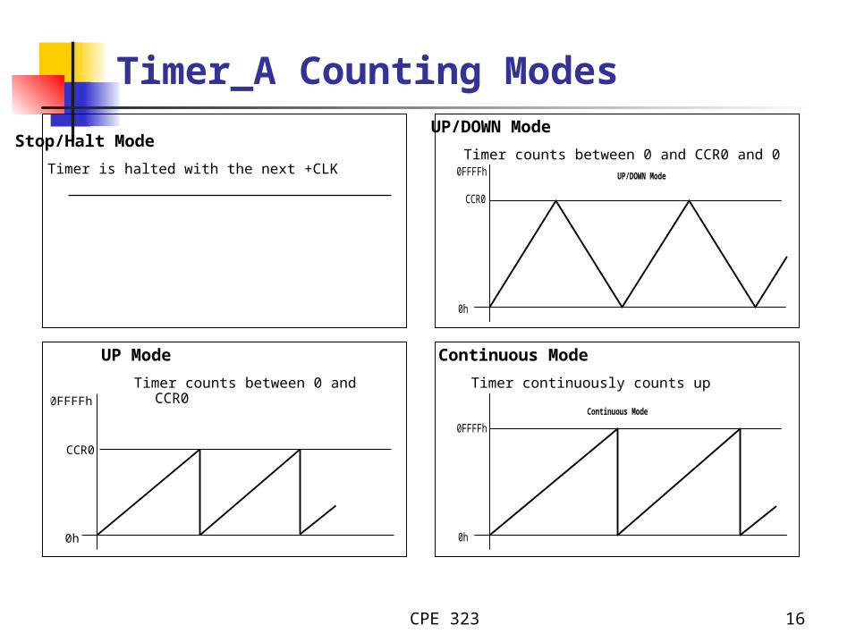
0FFFFh
0h
CCR0
Stop/Halt Mode
Timer is halted with the next +CLK
UP Mode
Timer counts between 0 and CCR0
0FFFFh
0h
CCR0
UP/DOWN Mode
Continuous Mode
0FFFFh
0h
Continuous Mode
Timer continuously counts up
UP/DOWN Mode
Timer counts between 0 and CCR0 and 0
Timer_A Counting Modes

CPE 323 17
Timer_A 16-bit Counter
Stop Mode Up ModeContinuous ModeUp/Down Mode
0 00 11 01 1
CLRDividerInput
SelectInput unused un-
usedTAIFGTAIE
015
160h
TACTL
rw-(0)
rw-(0)
rw-(0)
rw-(0)
rw-(0)
rw-(0)
rw-(0)
rw-(0)
rw-(0)
rw-(0)
rw-(0)
rw-(0)
rw-(0)
rw-(0)
rw-(0)
(w)-(0)
ControlMode
1/2 1/4 1/8
1/1, Pass0 00 11 01 1
0 00 11 01 1
ACLK MCLK
INCLK (often = #TACLK)
TACLK
MC0MC1
ID1 ID0
SSEL0SSEL1
TACLR – clears TAR and resets the direction of counting (it clears automatically itself)
TAIFG – set when the timer counts to 0; a maskable interrupt is requested if TAIE bit is set

CPE 323 18
0
162h
CCTLx
rw-
15
un-SCS OUTMODx
(0)rw-(0)
CAPINPUTSELECT
CAPTUREMODE
rrw-(0)
rw-(0)
rw-(0)
rw-(0)
rw-(0)
rw-(0)
rw-(0)
rw-(0)
rw-(0)
rw-(0)
rw-(0)
rw-(0)
CCIFGCOVOUTCCICCIE
16Ehto
rw-(0)
SCCI used
015CCRx
rw-(0)
rw-(0)
rw-(0)
rw-(0)
rw-(0)
rw-(0)
rw-(0)
rw-(0)
rw-(0)
rw-(0)
rw-(0)
rw-(0)
rw-(0)
rw-(0)
rw-(0)
rw-(0)
02
152
0172hto017Eh
to Port0
15 0
Capture/Compare Register CCRx
Comparator x
Overflow xLogic Data Bus Timer Bus
015
EQUxCAPx
0
COVx
Capture
DisabledPos. EdgeNeg. EdgeBoth Edges1 1
010 10 0
CMx1 CMx0
CMPx
TimerClock
1
0
SCSx
CCISx0
23
CCISx1
01CCIxB
VCCGND
CCIxA
CCIx
Capture Path
Compare Path Set_CCIFGx1
SCCIxENA Y
SynchronizeCapture
CaptureMode
Timer_A Capture Compare Blocks

CPE 323 19
TACCTLn: Capture Control CMx (Capture Mode)
00 – disabled 01 – positive edge 10 – negative edge 11 – both edges
CCISx (Capture Input Select) 00 – CCInA (outside timer) 01 – CCInB (outside timer) 10 – Gnd (pointless, but allows captures from SW) 11 – Vdd (pointless, but allows captures from SW) (for SW-triggered captures: use CMx=11, set CCIS1=1, and toggle CCIS0)
CCI –the state of the selected input can be read at any time from SW Race conditions: the selected input changes at the same time as the timer
clock SCS – synchronizer bit ensures synchronization with the timer clock
(SHOULD always be set) Capture: TAR is copied into TACCRn, the channel flag CCIFGn is set, and
a maskable interrupt is requested if bit CCIE in TACCTLx is set COV: Capture Overflow (next capture occurs before the TACCRn has been
read following the previous event)
CPE 323 20
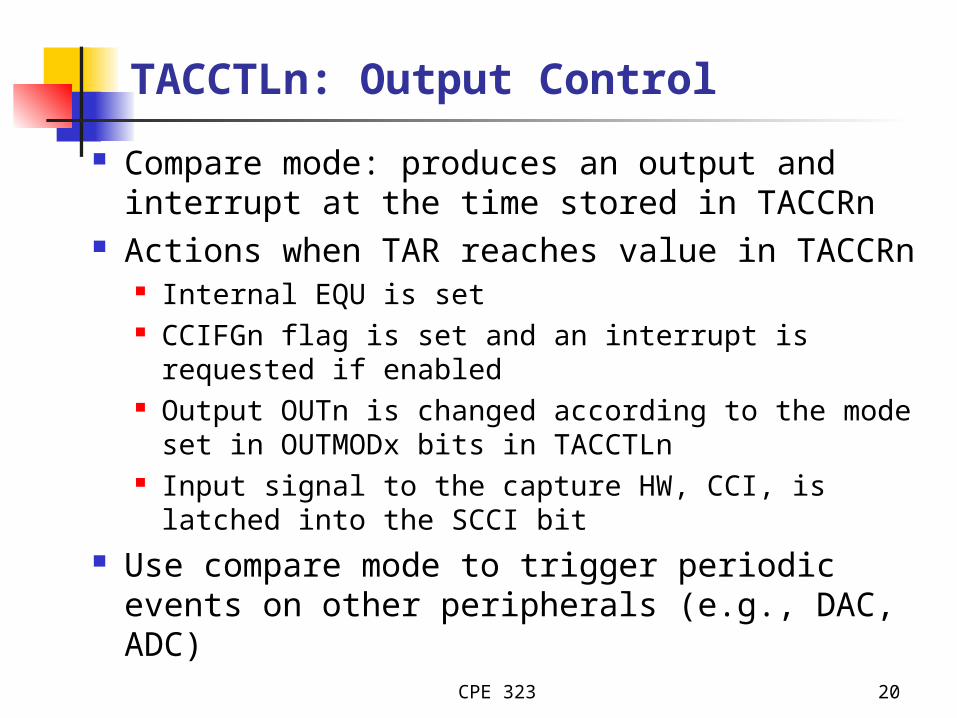
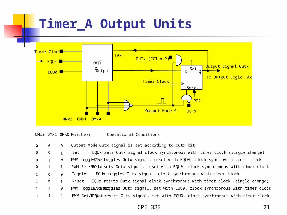
TACCTLn: Output Control
Compare mode: produces an output and interrupt at the time stored in TACCRn
Actions when TAR reaches value in TACCRn Internal EQU is set CCIFGn flag is set and an interrupt is requested if
enabled Output OUTn is changed according to the mode set
in OUTMODx bits in TACCTLn Input signal to the capture HW, CCI, is latched into
the SCCI bit Use compare mode to trigger periodic events on
other peripherals (e.g., DAC, ADC)
CPE 323 21
1 1 1 PWM Set/Reset EQUx resets Outx signal, set with EQU0, clock synchronous with timer clock
0
0 0
OMx1 OMx0OMx2
0
0
0
0
Set
PWM Toggle/Reset
PWM Set/Reset
1
1
1
1
1
0
0
1
0
1
1
0
0
1 Reset
PWM Toggle/Reset
Output Mode
Toggle
Outx signal is set according to Outx bit
EQUx sets Outx signal clock synchronous with timer clock (single change)
EQUx toggles Outx signal, reset with EQU0, clock sync. with timer clock
EQUx sets Outx signal, reset with EQU0, clock synchronous with timer clock
EQUx toggles Outx signal, clock synchronous with timer clock
EQUx resets Outx signal clock synchronous with timer clock (single change)
EQUx toggles Outx signal, set with EQU0, clock synchronous with timer clock
Function Operational Conditions
OUTx (CCTLx.2)
OMx2 OMx1 OMx0
EQUx
EQU0Set
Reset
D Q
OUTx
Timer Clock
POR
TAx
Output Mode 0
Logic
OutputOutput Signal Outx
To Output Logic TAx
Timer Clock
Timer_A Output Units

CPE 323 22
Output Mode Examples (UP)

CPE 323 23
Output Mode Examples (UP/DOWN)

CPE 323 24
Example shows three independent HW event captures. CCRx “stamps” time of event - Continuous-Mode is ideal.
0h
0FFFh
Capture Mode: Positive Edge
CCR1
CCR0
CCR1 CCR1
CCR0
TA0 Input
CCR1:
CCR1 CCR1
CCR2
TA1 Input
CCR0:
CCR2:TA2 Input
CCR1
Capture Mode: Both Edges
Capture Mode: Negative Edge
Interrupts can be generated
Px.x
Px.y
Px.z
Timer_A Continuous-Mode Example
CPE 323 25
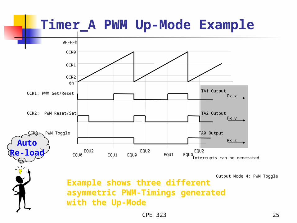
Output Mode 4: PWM Toggle
Example shows three different asymmetric PWM-Timings generated with the Up-Mode
AutoRe-load
0FFFFh
0h
CCR0
CCR1
EQU0 EQU0EQU1 EQU1 EQU0
CCR2
TA1 Output
CCR2: PWM Reset/Set
EQU2 EQU2 EQU2
Interrupts can be generated
TA2 Output
CCR1: PWM Set/Reset
CCR0: PWM Toggle TA0 Output
Px.x
Px.y
Px.z
Timer_A PWM Up-Mode Example

CPE 323 26
Example shows Symmetric PWM Generation - Digital Motor Control
0FFFFh
0h
CCR0
TIMOV EQU0 TIMOV
CCR1
EQU0
CCR2
Interrupts can be generated
tpw2
tpw3
CCR3
pw1t
0 Degrees
+120 Degrees
-120 Degrees
TIMOV
hlfpert
(0.5xVmotor)
(0.93xVmotor)
(0.07xVmotor)
TA1 Output
TA2 Output
TA0 Output
Px.x
Px.y
Px.z
Timer_A PWM Up/Down Mode Example

CPE 323 27
Interrupts from TImer_A
Sources: when TAIFG and CCIFG bit in each TACCTLn is set (CCIFGn for short)
TACCR0 is privileged (has higher priority than others) and has its own vector TIMERA0_VECTOR (single source)
TIMERA1_VECTOR is shared by the others (TAIFG + CCIFGx, x=1,2, ...) (multi source)
Inspecting individual flags can take a lot of time in ISR => Timer_A uses TAIV – interrupt vector register to identify the source of the interrupt rapidly
When one or more of the shared and enabled interrupts is set, TAIV is loaded with the value that corresponds to the highest priority

CPE 323 28
Timer_A Interrupt Service Routines

CPE 323 29
TAIV

CPE 323 30
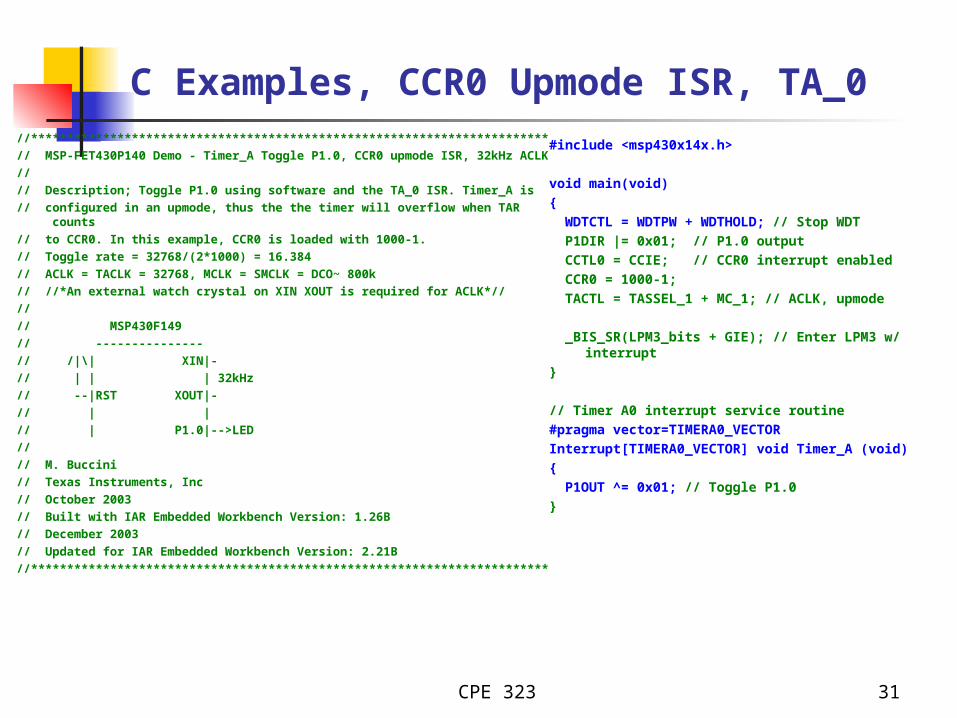
C Examples, CCR0 Contmode ISR, TA_0 ISR
//***************************************************************
// MSP-FET430P140 Demo - Timer_A Toggle P1.0,
// CCR0 Contmode ISR, DCO SMCLK
// Description; Toggle P1.0 using software and TA_0 ISR. Toggle rate is
// set at 50000 DCO/SMCLK cycles. Default DCO frequency used for TACLK.
// Durring the TA_0 ISR P0.1 is toggled and 50000 clock cycles are added to
// CCR0. TA_0 ISR is triggered exactly 50000 cycles. CPU is normally off and
// used only durring TA_ISR.
// ACLK = n/a, MCLK = SMCLK = TACLK = DCO~ 800k
//
//
// MSP430F149
// ---------------
// /|\| XIN|-
// | | |
// --|RST XOUT|-
// | |
// | P1.0|-->LED
//
// M. Buccini
// Texas Instruments, Inc
// September 2003
// Built with IAR Embedded Workbench Version: 1.26B
// December 2003
// Updated for IAR Embedded Workbench Version: 2.21B
//**********************************************************************
#include <msp430x14x.h>
void main(void)
{
WDTCTL = WDTPW + WDTHOLD; // Stop WDT
P1DIR |= 0x01; // P1.0 output
CCTL0 = CCIE; // CCR0 interrupt enabled
CCR0 = 50000;
TACTL = TASSEL_2 + MC_2; // SMCLK, contmode
_BIS_SR(LPM0_bits + GIE); // Enter LPM0 w/ interrupt
}
// Timer A0 interrupt service routine
interrupt[TIMERA0_VECTOR] void TimerA(void)
{
P1OUT ^= 0x01; // Toggle P1.0
CCR0 += 50000; // Add Offset to CCR0
}
CPE 323 31
C Examples, CCR0 Upmode ISR, TA_0//************************************************************************
// MSP-FET430P140 Demo - Timer_A Toggle P1.0, CCR0 upmode ISR, 32kHz ACLK
//
// Description; Toggle P1.0 using software and the TA_0 ISR. Timer_A is
// configured in an upmode, thus the the timer will overflow when TAR counts
// to CCR0. In this example, CCR0 is loaded with 1000-1.
// Toggle rate = 32768/(2*1000) = 16.384
// ACLK = TACLK = 32768, MCLK = SMCLK = DCO~ 800k
// //*An external watch crystal on XIN XOUT is required for ACLK*//
//
// MSP430F149
// ---------------
// /|\| XIN|-
// | | | 32kHz
// --|RST XOUT|-
// | |
// | P1.0|-->LED
//
// M. Buccini
// Texas Instruments, Inc
// October 2003
// Built with IAR Embedded Workbench Version: 1.26B
// December 2003
// Updated for IAR Embedded Workbench Version: 2.21B
//************************************************************************
#include <msp430x14x.h>
void main(void)
{
WDTCTL = WDTPW + WDTHOLD; // Stop WDT
P1DIR |= 0x01; // P1.0 output
CCTL0 = CCIE; // CCR0 interrupt enabled
CCR0 = 1000-1;
TACTL = TASSEL_1 + MC_1; // ACLK, upmode
_BIS_SR(LPM3_bits + GIE); // Enter LPM3 w/ interrupt
}
// Timer A0 interrupt service routine
#pragma vector=TIMERA0_VECTOR
Interrupt[TIMERA0_VECTOR] void Timer_A (void)
{
P1OUT ^= 0x01; // Toggle P1.0
}

CPE 323 32
C Examples, CCR1 Contmode ISR, TA_1//*****************************************************************
// MSP-FET430P140 Demo –
// Timer_A Toggle P1.0, CCR1 Contmode ISR, CO SMCLK
// Description; Toggle P1.0 using using software and TA_1 ISR.
// Toggle rate is set at 50000 DCO/SMCLK cycles.
// Default DCO frequency used for TACLK.
// Durring the TA_1 ISR P0.1 is toggled and
// 50000 clock cycles are added to CCR1.
// TA_1 ISR is triggered exactly 50000 cycles.
// CPU is normally off and used only durring TA_ISR.
// ACLK = n/a, MCLK = SMCLK = TACLK = DCO ~ 800k
// Proper use of TAIV interrupt vector generator demonstrated.
//
// MSP430F149
// ---------------
// /|\| XIN|-
// | | |
// --|RST XOUT|-
// | |
// | P1.0|-->LED
//
// M. Buccini
// Texas Instruments, Inc
// September 2003
// Built with IAR Embedded Workbench Version: 1.26B
// December 2003
// Updated for IAR Embedded Workbench Version: 2.21B
//**************************************************************
#include <msp430x14x.h>
void main(void){ WDTCTL = WDTPW + WDTHOLD; // Stop WDT P1DIR |= 0x01; // P1.0 output CCTL1 = CCIE; // CCR1 interrupt enabled CCR1 = 50000; TACTL = TASSEL_2 + MC_2; // SMCLK, Contmode
_BIS_SR(LPM0_bits + GIE); // Enter LPM0 w/ interrupt
}// Timer_A3 Interrupt Vector (TAIV) handler#pragma vector=TIMERA1_VECTOR__interrupt void Timer_A(void){ switch( TAIV ) { case 2: // CCR1 { P1OUT ^= 0x01; // Toggle P1.0 CCR1 += 50000; // Add Offset to CCR1 } break; case 4: break; // CCR2 not used case 10: break; // overflow not used }}

CPE 323 33
C Examples, PWM, TA1-2 upmode//***************************************************************************
// MSP-FET430P140 Demo - Timer_a PWM TA1-2 upmode, DCO SMCLK
//
// Description; This program will generate a two PWM outputs on P1.2/1.3 using
// Timer_A in an upmode. The value in CCR0, defines the period and the
// values in CCR1 and CCR2 the duty PWM cycles. Using ~ 800kHz SMCLK as TACLK,
// the timer period is ~ 640us with a 75% duty cycle on P1.2 and 25% on P1.3.
// ACLK = na, SMCLK = MCLK = TACLK = default DCO ~ 800kHz.
//
// MSP430F149
// -----------------
// /|\| XIN|-
// | | |
// --|RST XOUT|-
// | |
// | P1.2|--> CCR1 - 75% PWM
// | P1.3|--> CCR2 - 25% PWM
//
// M.Buccini
// Texas Instruments, Inc
// September 2003
// Built with IAR Embedded Workbench Version: 1.26B
// January 2004
// Updated for IAR Embedded Workbench Version: 2.21B
//*****************************************************
void main(void)
{
WDTCTL = WDTPW + WDTHOLD; // Stop WDT
P1DIR |= 0x0C; // P1.2 and P1.3 output
P1SEL |= 0x0C; // P1.2 and P1.3 TA1/2 options
CCR0 = 512-1; // PWM Period
CCTL1 = OUTMOD_7; // CCR1 reset/set
CCR1 = 384; // CCR1 PWM duty cycle
CCTL2 = OUTMOD_7; // CCR2 reset/set
CCR2 = 128; // CCR2 PWM duty cycle
TACTL = TASSEL_2 + MC_1; // SMCLK, up mode
_BIS_SR(LPM0_bits); // Enter LPM0
}