Cornell University Autonomous Underwater Vehicle Team...
13
Cornell University Autonomous Underwater Vehicle Team Fall 2014 Hydrophones Thumper Board v3.0 Technical Report Brook Du (xd47) May 10, 2014
Transcript of Cornell University Autonomous Underwater Vehicle Team...

Cornell University AutonomousUnderwater Vehicle Team
Fall 2014
Hydrophones ThumperBoard v3.0
Technical ReportBrook Du (xd47)
May 10, 2014
Thumper Board - v3.0
Contents
1 Abstract 2
2 Design Requirements 2
3 Previous Designs 3
4 High Level Description 3
5 Testing and Known Issues 35.1 DAC . . . . . . . . . . . . . . . . . . . . . . . . . . . . . . . . 45.2 DCDC . . . . . . . . . . . . . . . . . . . . . . . . . . . . . . . 45.3 Modulation . . . . . . . . . . . . . . . . . . . . . . . . . . . . 5
5.3.1 Delta-Sigma Modulation . . . . . . . . . . . . . . . . . 55.3.2 Pulse-Width Modulation . . . . . . . . . . . . . . . . . 5
5.4 Output Channel . . . . . . . . . . . . . . . . . . . . . . . . . 6
6 Current Status 6
7 Future Work 6
A Appendix 8A.1 References . . . . . . . . . . . . . . . . . . . . . . . . . . . . . 8A.2 Schematics . . . . . . . . . . . . . . . . . . . . . . . . . . . . 9
A.2.1 Corrected DCDC . . . . . . . . . . . . . . . . . . . . 9A.2.2 DAC . . . . . . . . . . . . . . . . . . . . . . . . . . . . 9A.2.3 Delta-sigma modulation . . . . . . . . . . . . . . . . . 10A.2.4 PWM . . . . . . . . . . . . . . . . . . . . . . . . . . . 10A.2.5 Output Channel 1 . . . . . . . . . . . . . . . . . . . . 11A.2.6 Output Channel 1 . . . . . . . . . . . . . . . . . . . . 11
A.3 PCB layout . . . . . . . . . . . . . . . . . . . . . . . . . . . . 12
1 Fall 2014

Thumper Board - v3.0
1 Abstract
The thumper board is an active hydrophone device that can be connected tothe current hydrophones backplane board as an extension. It can be used asan active sonar underwater or even communicate with other acoustic devicessuch as a pinger. This third version of the thumper board aims to addressthe issues and problems that have been encountered in the previous versionsand hence is significantly different from previous versions, featuring class Damplifiers, delta-sigma modulation and full H bridge driver circuits. It isintended to be a prototype board only with two output channels and twomodulators for testing purposes. This thumper prototype has 2 differentmodulating circuits implementation and 2 different amplication circuits im-plementation which yields 2*2 = 4 different ways of implementing a channel.
The actual thumper board in production should have at least 4 channelsand each channel can simply implement one of the four different ways ex-plored on the prototype board. It should also be condensed enough so thatit is able to fit in the hydrophones enclosure. Both the prototype board andthe production board should output frequency at 50 Hz.
2 Design Requirements
The main purpose of this prototype board is to explore the best ways tomodulating and amplifying the signal provided by the backplane board andproduce a sinusoidal signal with sufficent amplitude at 50 kHz. To be morespecific, this entails
• two proposed ways of modulations: delta-sigma modulation and PWM
• two propoesd structures of output channels which drive piezo elementsat 50 kHz
• ability to power up from +12 V supplied from the hydrophones back-plane board to + 90V from a custom DCDC which aims to resolve theissue of power amplification without current limiting and slow switch-ing op-amps
• ability to be connected and communicated with the hydrophones back-plane board
2 Fall 2014

Thumper Board - v3.0
3 Previous Designs
The major problem encountered in the previous versions of thumper boardwas power amplification. Thumper V2.0 had frequent current limiting dueto hugh current consumption from the NPN BJT/NMOS cascade sectionof the output amplifier whereas thumper V1.0 had op-amps which couldnot switch fast enough in the H-bridge. Therefore, the current version willadopt an entirely different way of stepping up the voltage from 12 V by acustom DCDC and use class D amplifiers in the output channel that canbe controlled by a potentiometer. This design is intended to avoid thesituation in which a single NMOS can be turned on at all times. Also,previous versions does not have any modulators on the board which willbe explored and prototyped in conjunction with class D amplifiers in thecurrent version.
4 High Level Description
As illustrated in the diagram below:
5 Testing and Known Issues
Currently the components which have been completely implemented andproven functioning correctly are the DAC circuits and the PWM modulatingchannel. The issues and results of these components are detailed below
3 Fall 2014
Thumper Board - v3.0
5.1 DAC
The DAC circuit implemetation is exactly the same as in thumper V2.0which was correctly implemented and fully tested. The circuit used thesame DAC chip, 12-bit dual channel AD5722R. Therefore for the sake ofonly the prototype board, the DAC circuit can be left unimplemented andsimply inject an analog signal from a function generator into an appropriatedtest point. For details of the design of the DAC circuit, please refer to thedesign documentation of thumper V2.0 and use exactly the same schematicsdesign which can be found in both thumper V3.0 and thumper V2.0.
5.2 DCDC
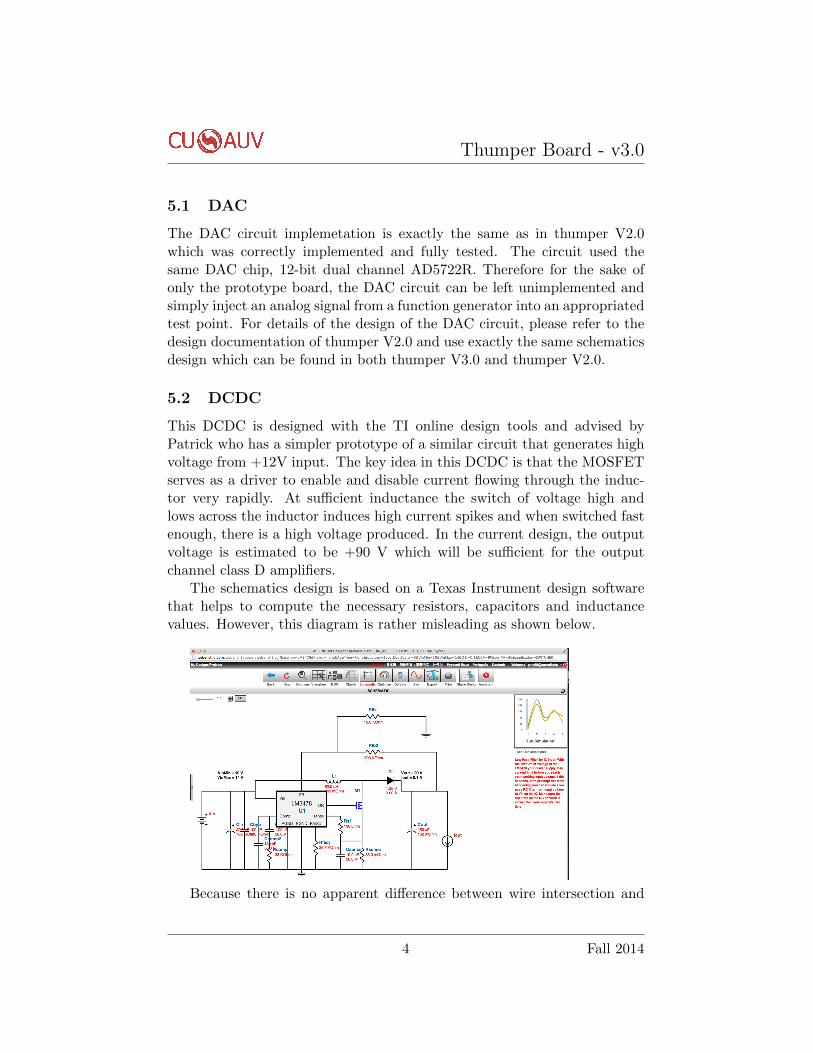
This DCDC is designed with the TI online design tools and advised byPatrick who has a simpler prototype of a similar circuit that generates highvoltage from +12V input. The key idea in this DCDC is that the MOSFETserves as a driver to enable and disable current flowing through the induc-tor very rapidly. At sufficient inductance the switch of voltage high andlows across the inductor induces high current spikes and when switched fastenough, there is a high voltage produced. In the current design, the outputvoltage is estimated to be +90 V which will be sufficient for the outputchannel class D amplifiers.
The schematics design is based on a Texas Instrument design softwarethat helps to compute the necessary resistors, capacitors and inductancevalues. However, this diagram is rather misleading as shown below.
Because there is no apparent difference between wire intersection and
4 Fall 2014

Thumper Board - v3.0
wire electrical connection in the diagram, there have been a few schematicserrors discovered due to careless interpretation of the diagram. It is to benoted that while Vin are not connected to FB at all, all the traces whichlook connected (e.g., traces from the port of Comp, AGND, PGND, FA/SD,Isense, and etc) are indeed connected and tied to ground. However, in thecurrent schematics, only Comp, AGND, FA/SD are electrically connectedand are not tied to the ground whereas the traces from the ports of PGND,Isense, Vin are connected and tied to the ground. This is probably thereason why the DCDC output voltage is still around +12V.
It should be also noted that the parts used in this DCDC circuit areexactly the ones recommended in the software which is also included inthe appendix. Only if the footprint is unrealistic, e.g. 0402 instead of0805, then the part can be replaced with an equivalent with a suitable andreasonalbe footprint. But for any part chosen to be different from the onesrecommended, one must verify that the ratings and other key features of thechosen part are in the same range of values.
5.3 Modulation
The purpose of modulation in the thumper board is to encode analog signalscoming from the DAC into digital signals. The purpose of modulating thesignals in this way is to firstly, reduce the noise which could be added duringtransmission and secondly, to make class D amplification easier because theoriginal waveform can be easily recovered from digital signals consisting ofseparated impulses. On the thumper board, we will explore two possibleways of modulation.
5.3.1 Delta-Sigma Modulation
The delta-sigam modulation has a fully functioning clock signal as of nowbut the rest of the circuit is still unimplemented.
5.3.2 Pulse-Width Modulation
The pulse-width modulation is another way of modulating the analog signalwe would like to explore for the thumper board. Pulse-width modulation is away of encoding analog signals by digital signals’ pulse width. The output ofa PWM modulator has pulses with various width that corresponds a samplevalue in the analog signal, for example, the value of a sine wave.
For this modulation, we have picked a convenient all-in-one part LTC6992 which can be conveniently configured at 1 MHz sampling rate.
5 Fall 2014

Thumper Board - v3.0
The correct behavior of the output from the PWM circuit has beenverifed on the oscilloscope and is shown below (diagram from datasheet):
5.4 Output Channel
Currently output channels have not been implemented because this channelcan only be implemented after DCDC is fully functionin.
6 Current Status
At the time that this report is written, the DCDC schematics is being re-viewed. As several mistakes have been discovered and are probably thereason why the DCDC is not working correctly, the board needs either ex-tensive rework wire or a second pcb revision. For now, rework wires arefaster solution and easier to implement to verify the correct schematics buta second pcb revision V3.1 is definitey necessary if there is more time.
7 Future Work
After the DCDC circuit is correctly implemented and tested, the only com-ponents left are the H-bridge (Class D amplifiers) in the output amplificationchannel.
6 Fall 2014
Thumper Board - v3.0
Future work on the thumper prototype board should also connect theboard to at least one piezo element on one of the two channels to make surethe signals are strong enough. Signal frequency, however, can be tested onthe bench via oscilloscope.
Another important aspect of the thumper board which has not been at-tempted is the software. There is no code that needs to be flashed to thethumper board, but the current hydrophones software only implements apassive hydrophones system. With thumper board working and in produc-tion, it is advised to also start implementing the necessary software, eitherin SHARC DSP or in future hydrocycle projects, to propoerly use the ac-tive sonar functionality so that the hydrophones system can also process thethumper signals reflected from objects under the water.
Thumper board is one of the most tricky boards on the team mainllybecause it is operating at 90V which is probably the highest voltage wehave seen on the electrial team. Therefore extreme cares should be takenwhen handling the board when it is powered. These include removing allaccessories, preferrably wearing wrist band which is attached to a groundedelectrical mat, making sure no statics accumulated and of course, wearingsafety goggles.
7 Fall 2014

Thumper Board - v3.0
A Appendix
A.1 References
DCDC part list
PWM modulator LTC6992 modulator datasheetOp-Amp LPC 6090 (op-amp) Datasheet
N-MOS controller for DCDC LM3478 DatasheetN-MOS for DCDC Si4488DY Datasheet
N-MOS for class D amplifier SiHFL110 datasheetP-MOS for class D amplifier SiHFL9110 Datasheet
Class D audio driver Si824x datasheet
8 Fall 2014

Thumper Board - v3.0
A.2 Schematics
A.2.1 Corrected DCDC
A.2.2 DAC
9 Fall 2014

Thumper Board - v3.0
A.2.3 Delta-sigma modulation
A.2.4 PWM
10 Fall 2014

Thumper Board - v3.0
A.2.5 Output Channel 1
A.2.6 Output Channel 1
11 Fall 2014
Thumper Board - v3.0
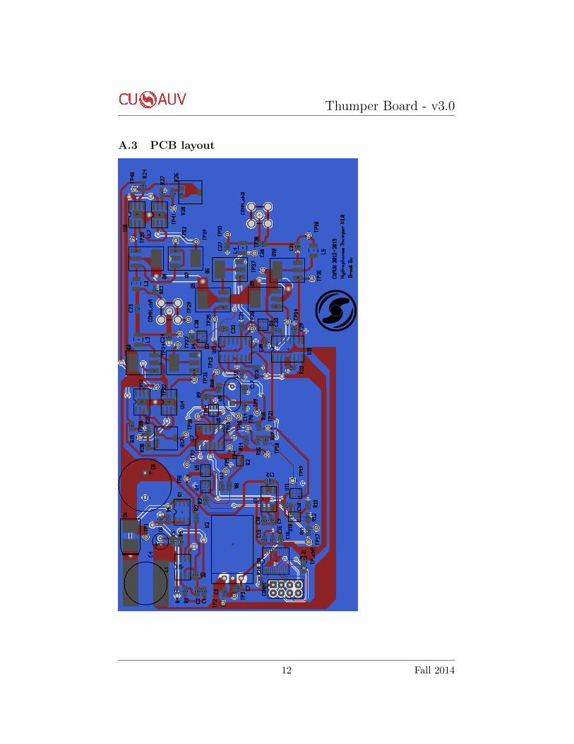
A.3 PCB layout
12 Fall 2014