
CoreSight SoC enabling efficient design of custom debug ... · Copyright © 2014 ARM Limited or its...
21
Copyright © 2014 ARM Limited or its affiliates. All rights reserved. ARM is a registered trademark of ARM, Limited in the EU and/or elsewhere. All rights reserved. All other trademarks are the property of their respective owners and are acknowledged. Page 1 of 21 CoreSight SoC enabling efficient design of custom debug and trace subsystems for complex SoCs Key steps to create a debug and trace solution for an ARM SoC Mayank Sharma, Technical Marketing Engineer, Systems and Software Group, ARM ABSTRACT MIPI Alliance – Architecture Overview of Debug 1 : “It has become an accepted axiom that as the complexity of an embedded system increases, the need for system designers and developers to obtain visibility into the behavior of the system increases proportionally.” Cambridge University Study 2 : “The global cost of debugging software has risen to $312 billion annually. The research found that, on average, software developers spend 50% of their programming time finding and fixing bugs.” ITRS annual design report 3 : “Software aspects of IC design can now account for 80% or more of embedded systems development cost.” To address the challenge of increasing development cost and complexity faced by the semiconductor industry, SoC designers need to think ahead and provide the right hardware platform to help software developers create optimized software in a timely manner. The goal of this paper is to show, through high level steps, how to create a custom debug and trace subsystem for a design quickly and easily. This paper will be of interest to those who want to learn about debug and trace for System-on-Chips (SoCs) and be of specific interest to the following: Product Managers who want their SoC product to be developed faster (hardware/software co- development, early bring-up of silicon for faster time-to-market), to be more robust (fewer bugs and reduced debug time) and to be performant (profiling, benchmarking and optimization). SoC architects interested in building reliable, advanced and efficient debug and trace solutions for their SoCs with reduced time and effort. 1 http://mipi.org/whitepaper/mipi-mipi-debug-architecture-overview 2 http://www.jbs.cam.ac.uk/media/2013/financial-content-cambridge-university-study-states-software-bugs-cost- economy-312-billion-per-year 3 http://www.itrs.net/Links/2007ITRS/2007_Chapters/2007_Design.pdf
Transcript of CoreSight SoC enabling efficient design of custom debug ... · Copyright © 2014 ARM Limited or its...

Copyright © 2014 ARM Limited or its affiliates. All rights reserved. ARM is a registered trademark of ARM, Limited in the EU and/or elsewhere. All rights reserved.
All other trademarks are the property of their respective owners and are acknowledged.
Page 1 of 21
CoreSight SoC enabling efficient design of custom
debug and trace subsystems for complex SoCs Key steps to create a debug and trace solution for an ARM SoC
Mayank Sharma, Technical Marketing Engineer, Systems and Software Group, ARM
ABSTRACT
MIPI Alliance – Architecture Overview of Debug1: “It has become an accepted axiom that as the
complexity of an embedded system increases, the need for system designers and developers to obtain
visibility into the behavior of the system increases proportionally.”
Cambridge University Study2: “The global cost of debugging software has risen to $312 billion annually.
The research found that, on average, software developers spend 50% of their programming time finding
and fixing bugs.”
ITRS annual design report3: “Software aspects of IC design can now account for 80% or more of
embedded systems development cost.”
To address the challenge of increasing development cost and complexity faced by the semiconductor
industry, SoC designers need to think ahead and provide the right hardware platform to help software
developers create optimized software in a timely manner. The goal of this paper is to show, through
high level steps, how to create a custom debug and trace subsystem for a design quickly and easily. This
paper will be of interest to those who want to learn about debug and trace for System-on-Chips (SoCs)
and be of specific interest to the following:
Product Managers who want their SoC product to be developed faster (hardware/software co-
development, early bring-up of silicon for faster time-to-market), to be more robust (fewer bugs
and reduced debug time) and to be performant (profiling, benchmarking and optimization).
SoC architects interested in building reliable, advanced and efficient debug and trace solutions
for their SoCs with reduced time and effort.
1 http://mipi.org/whitepaper/mipi-mipi-debug-architecture-overview
2 http://www.jbs.cam.ac.uk/media/2013/financial-content-cambridge-university-study-states-software-bugs-cost-
economy-312-billion-per-year
3 http://www.itrs.net/Links/2007ITRS/2007_Chapters/2007_Design.pdf
Copyright © 2014 ARM Limited or its affiliates. All rights reserved. ARM is a registered trademark of ARM, Limited in the EU and/or elsewhere. All rights reserved.
All other trademarks are the property of their respective owners and are acknowledged.
Page 2 of 21
Software architects who want to understand the capabilities of debug and trace hardware and
tools to help them create optimized software. It will also allow software developers to drive
conversations with SoC designers to get the necessary hardware hooks as needed.
Hardware Engineers, using ARM CoreSight SoC technology, who want to learn how to design a
custom debug and trace solution in a day!
INTRODUCTION
Modern SoCs are continually increasing in complexity and packing in more and more features. Large
designs with multiple CPU architectures, GPUs, numerous power domains, various DVFS regions,
big.LITTLE and advanced security schemes are very common. This in turn adds a big overhead for silicon
bring-up and software development/optimization. Meanwhile designers are under increased pressure to
keep the costs down.
Given that the cost of bugs is already very high and is set to rise, technologies which reduce debugging
time have the potential to make a real impact on the semiconductor industry and the global economy in
general. Traditional hardware debug solutions fail to address the entire SoC space, where a configurable
debug and trace solution, customized for the SoC, is essential for hardware debug, software
development, performance analysis and optimization. Furthermore, in order to maximize utility and
efficiency of debug, using common interfaces and protocols is important and this is where ARM’s
CoreSight technology is ideal.
This paper gives you an architect’s view of how to build a debug and trace solution for a typical ARM
SoC. It shows you how ARM CoreSight SoC technology (CoreSight SoC-400) is useful at each stage of the
SoC development cycle in enabling efficient design of custom debug and trace subsystems.
Copyright © 2014 ARM Limited or its affiliates. All rights reserved. ARM is a registered trademark of ARM, Limited in the EU and/or elsewhere. All rights reserved.
All other trademarks are the property of their respective owners and are acknowledged.
Page 3 of 21
Why bother with debug and trace?
The current trend in the electronics industry is towards increasingly complex hardware with ever-rising
software development costs with much-reduced time-to-market. Original Equipment Manufacturers
(OEMs) are expecting silicon providers to provide a reliable and complete hardware and software
system ready for applications development, and this is a key differentiator.
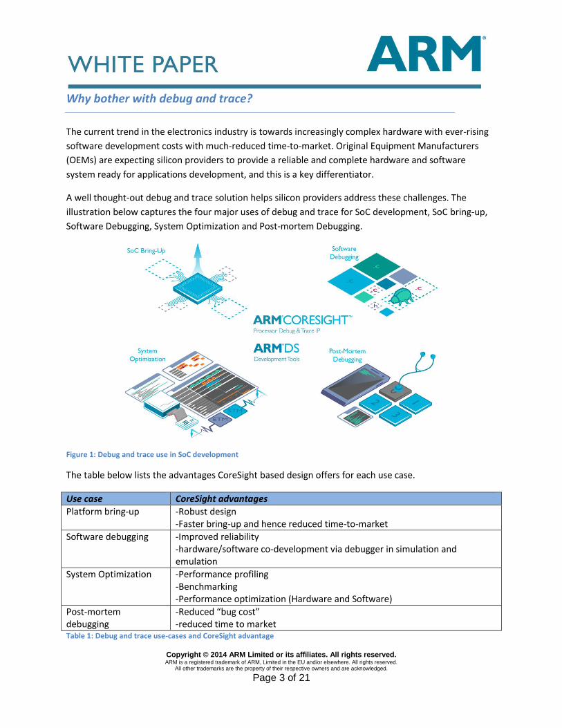
A well thought-out debug and trace solution helps silicon providers address these challenges. The
illustration below captures the four major uses of debug and trace for SoC development, SoC bring-up,
Software Debugging, System Optimization and Post-mortem Debugging.
Figure 1: Debug and trace use in SoC development
The table below lists the advantages CoreSight based design offers for each use case.
Use case CoreSight advantages
Platform bring-up -Robust design -Faster bring-up and hence reduced time-to-market
Software debugging -Improved reliability -hardware/software co-development via debugger in simulation and emulation
System Optimization -Performance profiling -Benchmarking -Performance optimization (Hardware and Software)
Post-mortem debugging
-Reduced “bug cost” -reduced time to market
Table 1: Debug and trace use-cases and CoreSight advantage

Copyright © 2014 ARM Limited or its affiliates. All rights reserved. ARM is a registered trademark of ARM, Limited in the EU and/or elsewhere. All rights reserved.
All other trademarks are the property of their respective owners and are acknowledged.
Page 4 of 21
What is CoreSight SoC-400?
CoreSight SoC-400 is a debug subsystem design and validation flow aimed at reducing risk, accelerating
and optimizing debug implementation in heterogeneous and multi-core SoCs. It provides a kit of parts
that you can use to build and validate debug and trace elements of a System-on-Chip allowing you to
create bespoke debug solutions for complex multi-processor SoCs. The table describes what is included
in the SoC-400 r3p1 product.
SoC-400 Component Description
Library of configurable components + configuration scripts
Verilog components to implement CoreSight functionality for debug, trace, cross-triggering and timestamps. Comes with scripts to render configured instances of the components based on the user requirements.
Optional GUI flow IP-XACT component views allow the user to graphically configure, integrate and stitch the components and ARM processors. ARMs AMBADesigner or other IP-XACT compatible stitching tools can be used.
Support for System Trace Macrocell (STM) & Trace Memory Controller (TMC) and Embedded Trace Macrocell (ETM)
These separately licensed components are supported within the SoC-400 flow of configuring and stitching components.
Support for processor debug integration
The most recently released processors natively support CoreSight SoC. Integration of older processors with CoreSight SoC is implemented using Processor Integration Layers (PILs), a wrapper layer that provides the required debug integration capability. This library can be licensed separately to meet your specific processor requirements.
Documentation SoC-400 consolidates the CoreSight component documentation for the latest generation of IP. It consists of a Technical Reference Manual, User Guide, Implementation Guide, System Design Guide and Integration Manual4 to help with your SoC design.
Validation Components CXDT (JTAG driver), C-language test cases, worked example designs and testbenches, protocol checkers and monitors
Table 2: SoC-400 components
Therefore, SoC-400 is used alongside ARM CPU products and advanced debug and trace components,
such as the STM and TMC, to build a comprehensive and custom SoC debug and trace solution.
4 SoC-400 User Guide, Implementation Guide, System Design Guide and Integration Manual are product
documents available to licensees

Copyright © 2014 ARM Limited or its affiliates. All rights reserved. ARM is a registered trademark of ARM, Limited in the EU and/or elsewhere. All rights reserved.
All other trademarks are the property of their respective owners and are acknowledged.
Page 5 of 21
Figure 2: Components required for building a debug and trace solution for an advanced ARM SoC
Debug and Trace Design Flow
The stages in developing a debug and trace solution for an SoC are shown in the figure below. The key is
to “think ahead” and have the relevant debug and trace architecture in place to meet specific
requirements. The illustration shows where the ARM SoC-400 product helps in each of the stages for
efficient design of complex debug and trace solutions.
Figure 3: Debug and Trace design for SoCs – recommended design Flow

Copyright © 2014 ARM Limited or its affiliates. All rights reserved. ARM is a registered trademark of ARM, Limited in the EU and/or elsewhere. All rights reserved.
All other trademarks are the property of their respective owners and are acknowledged.
Page 6 of 21
STEP 1: EVALUATE OPTIONS
The first step in the recommended design flow for debug and trace is the most important step and it
requires designers to “think ahead”. This ensures they have understood their design choices to pick the
right hardware to support the SoCs debug and trace use-cases. Below are some of the key design
considerations faced by SoC architects today.
Architectural Requirements
The CoreSight SoC debug solution supports all ARM processors and the CoreSight SoC IP components are
architecture agnostic. However, debug features available in each architecture might dictate certain
debug subsystem requirements. For example, the ARMv8 architecture uses 64 bit memory accesses and
so components should be chosen that support 64 bit memory accesses. Hence, the use of STM-500 is
recommended as it has native support for 64-bit accesses. Therefore, designers should refer to the
debug section of the ARM Architecture Reference Manuals (ARMv8, ARMv7, ARMv6) and Technical
Reference Manuals of ARM processors to understand the processor debug and trace requirements.
Hardware Tracing
Hardware tracing is an ability to observe the inner states of an SoC over a period of time in a non-
invasive manner. Hardware trace can monitor the execution of the program and might also monitor
the data transactions to and from memory. It does not require changing any aspect of the functional
program to collect data. This helps in debugging applications that involve timing errors, interrupt latency
issues, and other timing critical aspects. Hardware trace consists of a monitor for processor activity, a
trace distribution system and one or more trace capture devices that provide external access to the
captured data. ARM processors include activity monitoring capability while CoreSight SoC and the
“ETM” and “PTM” components provide the capability to process the data captured and to send it off
chip for analysis.
Trace bandwidth calculations
As very large quantities of data might be captured the architect must determine the limits for what
quantities of trace data will be captured on chip and determine the bandwidth of the trace distribution
network to support that capability. The debug system architect will need to consider the trade-offs
bandwidth, capture devices, silicon area/pin requirements etc.

Copyright © 2014 ARM Limited or its affiliates. All rights reserved. ARM is a registered trademark of ARM, Limited in the EU and/or elsewhere. All rights reserved.
All other trademarks are the property of their respective owners and are acknowledged.
Page 7 of 21
SoCs today have multiple trace sources such as ETMs for multiple processors and STM(s) for system
trace. This puts heavy bandwidth requirements on the system trace infrastructure. Although CoreSight is
designed with graceful degradation in the case that more trace is generated than can be captured, this is
not ideal. SoC-400 provides multiple features to give designers maximum flexibility when trying to meet
their SoC bandwidth requirements. The following can help with a designer’s decision making to address
this challenge.
- Careful use of filtering will result in more useful trace being captured than relying too much on
the overflow/recovery behavior. The new revisions of CoreSight IP supported in SoC-400 has
advanced filtering options such as priority settings on ATB Funnels and ID filtering on
Replicators.
- ARM processor licensees have access to information on how much trace (bits per instruction)
the ETMs generate. The demands of a trace source can vary greatly, an ETM trace unit might
produce between 1 bit per instruction for instruction only trace, or over 30 bits per instruction
when tracing instructions and data. Even if the data to be traced can be filtered, this might not
help much for short-term bursts of data; therefore, an on chip trace FIFO can help. For more
complex trace systems, this becomes a more cost-effective solution as the resource added is
shared between more of the trace logic. The user can select which trace source needs most
bandwidth, but still enable a smaller amount of trace from several other sources, or use the
other sources as triggering resources.
- The configurable trace components in SoC-400 (for example, Upsizers/Downsizers for trace data
width manipulations, asynchronous/synchronous bridges for going across clock/power domains,
Replicators and Funnels for trace flow setup supporting prioritization and filtering of trace)
provide great flexibility to SoC architects to help meet bandwidth requirements for an SoC.
Trace Capture Options
An advantage of using CoreSight components for implementing an SoC trace solution is that you have
support for multiple trace capture options. These options are capable of meeting various SoC specific
bandwidth requirements. Also, in most cases, the same hardware components can be configured via
software to support various trace capture modes.
Table 3: Trace capture options with SoC-400 describes common trace capture options enabled by
CoreSight, the hardware required, advantages of each and usage considerations for SoC designers.

Copyright © 2014 ARM Limited or its affiliates. All rights reserved. ARM is a registered trademark of ARM, Limited in the EU and/or elsewhere. All rights reserved.
All other trademarks are the property of their respective owners and are acknowledged.
Page 8 of 21
Trace
Capture
mode
Devices
Used
Capturing
Mechanism
Advantages Usage considerations
On-chip
SRAM
ETF
(circular
buffer
mode)/ETB
Trace capture in
dedicated SRAM as
stored in the ETF.
When capture stops,
you can access it via
a debugger
Fully non-
intrusive and high
bandwidth.
Limited depth
Can be read from target
software enabling in-field
debug
Physical trace port not
required on SoC
Off-chip
capture
device
ETF (HW-
FIFO mode)
+ TPIU
Trace capture in to
an off-chip capture
device with on-chip
buffering
Fully non-
intrusive and its
depth is limited
only by the off-
chip capture
device
Bandwidth is restricted by
the physical characteristics of
the trace port
The need to dedicate pins to
a trace port on your SoC
System
memory
ETF (HW-
FIFO mode)
+ ETR
Trace capture in
system memory with
intermediate
buffering. The
intermediate
buffering enables
trace to be resilient
to large delays on
the interconnect
Large depth of
trace capture
available. Trace
port not required
Intrusive to system
performance (less memory
available to the rest of the
system, bandwidth of the
DMC must be shared
between the ETR and regular
system functions)
Can be read from target
software enabling in-field
debug
Debugger
Capture
ETF (SW-
FIFO mode)
Low-speed off-chip
trace capture
through the DAP
Fully non-
intrusive and high
depth. ETR and
TPIU disabled
Limited bandwidth
Table 3: Trace capture options with SoC-400
All of the above can be implemented using the TMC components (in different configurations such as
ETF, ETR or ETB) alongside CoreSight trace infrastructure components (Funnels, Upsizers, etc.). These
options are useful in trace bandwidth limited systems as they support multiple usage models.

Copyright © 2014 ARM Limited or its affiliates. All rights reserved. ARM is a registered trademark of ARM, Limited in the EU and/or elsewhere. All rights reserved.
All other trademarks are the property of their respective owners and are acknowledged.
Page 9 of 21
Software Tracing
Software tracing provides a mechanism to allow the processors/system masters to write
instrumentation i.e. “printf” styled messages out to the trace stream. Modern SoC designs require a
system wide approach and ARM addresses this via the System Trace Macrocell (STM). A debug and trace
solution can be architected where any system master can generate instrumentation via STM trace. Each
master is uniquely identified and STM also supports timestamps to correlate events across masters.
Using a generic solution such as an STM is less invasive as explicit production to standard output of run-
time information using software print statements is not needed.
Instrumenting hardware events
Another useful feature of the STM product is the support for capturing interesting hardware events in
the system and inserting them into the output trace stream. Examples of events wired to the STM are
interrupts, power/clock state-change signals, SoC specific signals, etc.
Multiple Trace Sources Correlation
For modern SoCs, it is important to analyse the system wide interactions and hence, correlation of trace
from multiple sources is essential. SoC-400 supports global timestamps that can be captured in various
trace streams (ETM, STM). SoC-400 supports timestamp distribution architecture for the entire SoC and
the following considerations are useful:
- The timestamp architecture generally includes timestamp bridges and replicators for the
distribution of time so it is important to consider the balancing of the timestamps distribution
tree to various trace sources. This helps with better accuracy on correlation of events.
- The trace sources in an SoC usually run on different clock frequencies and these result in a need
for a higher resolution of timestamp value on higher frequency trace sources for effective time-
based correlation between trace sources. See section 6.2.6 Timestamp interpolator of the
CoreSight SoC-400 System Design Guide5.
Debugger Access to system
There are a couple of options for an external debugger access to the memory and peripherals on an SoC.
One is for the debugger to halt CPUs and execute CPU instructions to access memory and peripherals.
The other option is for the debugger to be a system master and accesses memory and peripherals
directly. SoC-400 supports both of these options. For debugger as a system master, SoC-400 provides an
AXI-Access Port (AXI-AP) or AHB-AP to connect debugger to the SoC interconnects.
5 SoC-400 product documentation

Copyright © 2014 ARM Limited or its affiliates. All rights reserved. ARM is a registered trademark of ARM, Limited in the EU and/or elsewhere. All rights reserved.
All other trademarks are the property of their respective owners and are acknowledged.
Page 10 of 21
Physical memory vs Virtual memory
A consideration for SoC designers, who have a System Memory Management Unit (SMMU) in the
design, is whether to include an SMMU along the path of AXI-AP connection to the interconnect. This
raises the question of whether the debugger sees the “physical memory” or the “virtual memory”. An
approach is to provide the debugger the view of the “physical” memory by not including an SMMU along
its path to the interconnect. It can be argued that a debugger can access to the virtual memory via the
CPUs if needed.
Cross-communication of debug events
An important element of debugging an SoC is to detect and broadcast events across components. This
ability to “trigger” can be used, for example, to halt counters when CPU enters debug state or to halt
trace sources when trace buffers are full. SoC-400 provides CTI and CTM components that allow for
interconnectivity of these trigger inputs and outputs. This bit of architecture is SoC specific and
designers can choose how to connect these. CTI block should be used to connect signals in your design
so they can be used by debug tools and/or observed/controlled via software to help with debug
visibility. CTMs are used to connect multiple CTIs to create a “cross-triggering” network. Some useful
pointers for designing cross-trigger solution for ARM SoCs are provided below.
- ARM has recommendations on how ETR, ETF, STM and TPIU should be connected to a CTI. See
section 4.6 Typical trigger signals CoreSight SoC-400 System Design Guide
- The tie-offs are described in section 4.11.1 CTI tie-off signals and 4.11.2 CTM tie-offs in CoreSight
SoC-400 Integration Manual.
- Most cross triggering events go across clock and power boundaries and hence, these should be
passed through asynchronous event bridges to ensure the triggers are correctly captured by the
CTIs. Where possible, make use of the handshaking on each of the triggers even if the
acknowledge signal is a loop-back of the trigger from the receive domain. See section 8.4 Event
asynchronous bridge of the CoreSight SoC-400 Technical Reference Manual.
big.LITTLE debug – Multiple Power Domains
A big.LITTLE system implements a high-performance ARM CPU (big) cluster alongside a low-power one
(LITTLE). Each cluster has its own debug and trace functionality which is agnostic of a big.LITTLE
configuration. But to gain additional visibility into big.LITTLE specific features such as hardware
switching on/off, software threads migrating from one cluster to another and to optimize the
hardware/software, it is important to support certain key debug and trace functions that can be used by
the external debugger (see example of support in ARM DS-5 tool) to provide a user with useful
information.

Copyright © 2014 ARM Limited or its affiliates. All rights reserved. ARM is a registered trademark of ARM, Limited in the EU and/or elsewhere. All rights reserved.
All other trademarks are the property of their respective owners and are acknowledged.
Page 11 of 21
Below are some recommendations for debug support for big.LITTLE designs as provided in CoreSight
SoC.
Support cross-halting between big and LITTLE clusters by connecting the CTM channels for each
cluster on to the SoC cross-trigger network.
Partition CPU core and debug domains across power domains to ensure debug connectivity
during power down of clusters. This allows the debugger to correctly monitor and switch views
during big.LITTLE power-up and down.
To synchronize software execution across big and LITTLE cores, it is important to have an SoC
timestamp architecture that has a balanced distribution of timestamps to all the cores.
Self-Hosted Debug
This is an important consideration for modern SoCs that require debugging without actually connecting
an external debugger or need for external hardware. Having an ability to run self-hosted debug tools on
the SoC itself allows for:
- Post-mortem crash analysis using “flight-recorder” mode where trace data is captured during
execution for later analysis
- Remote debugging
- Performance analysis using trace
It is desirable to design an SoC to support both external debug and self-hosted debug. For successful
implementation of self-hosted debug the designer needs to consider the following:
- Provide system access to debug components over the debug APB bus. This is done by
configuring the APB-IC appropriately to differentiate system or external debug access. See
section 4.3.1 Debug Memory and 4.3.2 System Interface of the CoreSight SoC-400 System Design
Guide6.
- Provide control for debug authentication signals to support various self-hosted debug modes.
The different settings for DBGEN, NIDEN, SPIDEN and SPNIDEN signals can be found in section
4.1 Platform support for self-hosted debug and trace of Debug and Trace Configuration and
Usage Models.
- It is recommended to use TMC in ETR configuration to direct trace in to system memory and
save it on the chip. This can be accessed later by performance analysis tools and also useful for
“flight-recorder” mode post analysis.
6 SoC-400 product documentation
Copyright © 2014 ARM Limited or its affiliates. All rights reserved. ARM is a registered trademark of ARM, Limited in the EU and/or elsewhere. All rights reserved.
All other trademarks are the property of their respective owners and are acknowledged.
Page 12 of 21
STEP 2: REQUIREMENTS CAPTURE – WHAT DO I NEED?
STEP 1 requires that the SoC architects, software developers and product management have
constructive conversations to define the debug and trace functionality needed for their SoC solution.
STEP 2 matches these needs to specific component requirements. There is a wide range of debug and
trace functionality required in an SoC and CoreSight SoC-400 offers a large set of components to help
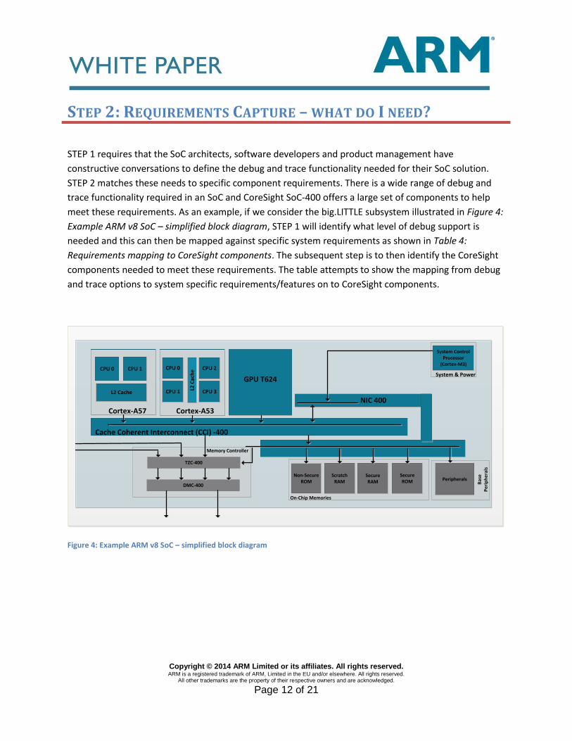
meet these requirements. As an example, if we consider the big.LITTLE subsystem illustrated in Figure 4:
Example ARM v8 SoC – simplified block diagram, STEP 1 will identify what level of debug support is
needed and this can then be mapped against specific system requirements as shown in Table 4:
Requirements mapping to CoreSight components. The subsequent step is to then identify the CoreSight
components needed to meet these requirements. The table attempts to show the mapping from debug
and trace options to system specific requirements/features on to CoreSight components.
CPU 0
Cortex-A57
DMC-400
System & Power
PeripheralsB
ase
Pe
rip
he
rals
CPU 1 CPU 0
Cortex-A53
CPU 2
Cache Coherent Interconnect (CCI) -400
NIC 400
On-Chip Memories
ScratchRAM
SecureRAM
SecureROM
Non-SecureROM
TZC-400
CPU 1 CPU 3
System Control Processor
(Cortex-M3)
L2 Cache
L2 C
ach
e
GPU T624
Memory Controller
Figure 4: Example ARM v8 SoC – simplified block diagram

Copyright © 2014 ARM Limited or its affiliates. All rights reserved. ARM is a registered trademark of ARM, Limited in the EU and/or elsewhere. All rights reserved.
All other trademarks are the property of their respective owners and are acknowledged.
Page 13 of 21
Debug and Trace Options
System Requirements Debug Components Mapping
Architectural Requirements
Cortex-A57/53: ARMv8, System Controller: ARMv7M
APB Control bus for Cortex-A57/53, DAPBUS Control bus for Cortex-M3
Hardware Tracing Cortex-A57/53 (ETMs): 32 bit trace bus per CPU, Cortex-M3: two (ITM & ETM) 8 bit trace buses
ETMs ATB Funnel, Replicator, Downsizer, Upsizer ETF & ETR (TMC) Asynchronous ATB bridges Synchronous ATB bridges
Software Tracing 64 Bit access support, Individual CPU cores, GPU, Debugger and other systems masters to generate instrumentation Instrumentation of power-control signals using the HWEVENTS interface
STM-500
Multiple Trace Sources Correlation
Debug timestamp distribution to Cortex-A57/53 and STM-500
Timestamp components Timestamp (TS) generator TS Interpolator Narrow Timestamp Asynchronous Bridges TS Encoder/Decoder
Debug Access to system Direct access to system memory and peripherals via the AXI interconnects. Provide access to “physical memory”
AXI-AP to connect debugger to NIC-400 interconnect
Cross-communication of debug events
CTM channels for Cortex-A57/53 clusters, CTI for Cortex-M3 events, CTI for CoreSight component trigger events (STM, ETF, ETR & TPIU). Interconnectivity of all triggers using CTM channels
CTIs CTMs Event Bridges for asynchronous crossing of events across clock and power domains
big.LITTLE debug – Multiple Power Domains
Cortex-A57 & Cortex-A53 in big.LITTLE configuration. Support for cross-halting via cross-trigger interfaces
Asynchronous bridges – ATB, APB and Event bridges CTI & CTM
Self-Hosted Debug Use ETR and its AXI port to route trace data to system memory via the fabric. Provide system masters to access CoreSight components via the interconnect. Also, add control for debug authentication signals
ETR Debug APB bus Debug authentication interface
Table 4: Requirements mapping to CoreSight components

Copyright © 2014 ARM Limited or its affiliates. All rights reserved. ARM is a registered trademark of ARM, Limited in the EU and/or elsewhere. All rights reserved.
All other trademarks are the property of their respective owners and are acknowledged.
Page 14 of 21
STEP 3: DESIGN – HOW DO I BUILD IT?
The recommended way to implement the CoreSight debug and trace solution is to split the functionality into four distinct subsystems: debug, trace, cross-trigger and timestamp. Some CoreSight components have functionality across each of the above elements so there is some overlap. But this approach helps with splitting the complex integration across the SoC in to manageable chunks of shared functionality. An example design steps across functionalities using SoC-400 components is given below.
Debug There are two key elements for debug control design. To provide access to debug and trace components and to set external debugger access points Hence, you would configure debug APB interconnect, DAP interconnect (AXI-AP, APB-AP, AHB-AP) and instantiate asynchronous and synchronous APB bridges for clock/power domain crossings.
Trace Once tracing options supported by the SoC are identified in the STEP 2, the design step involves configuring the TMC (for example, as ETF and/or ETR), configure ATB Upsizers and Downsizers where needed, configure ATB Funnels and replicators and instantiate asynchronous and synchronous bridges for clock/power domain crossings.
Cross Trigger CTI & CTM components have fixed configurations but individual trigger connectivity should be configured for handshaking and synchronization. This is to guarantee that trigger events are correctly seen by CTIs & CTMs.
Figure 5: Elements of debug and trace design
Copyright © 2014 ARM Limited or its affiliates. All rights reserved. ARM is a registered trademark of ARM, Limited in the EU and/or elsewhere. All rights reserved.
All other trademarks are the property of their respective owners and are acknowledged.
Page 15 of 21
Timestamp
Timestamp distribution requires the use of interpolator components that should be configured to meet
the clock frequency requirements for each trace source. Also, it is useful to balance the timestamp
distribution network across the SoC so each trace source sees (approximately) the same timestamp and
the use of asynchronous and synchronous bridges should be balanced.
Component Configurations
Having determined the functionality required for each subsystem the CoreSight SoC components will
need to be configured and then integrated within a subsystem and also across the SoC. CoreSight
components in SoC-400 can have multiple configurations to support a range of requirements. This
allows for an efficient design to suit different use models and get the maximum utilization of the
hardware. SoC-400 provides a script flow to configure components easily and this renders the
component RTL and an IPXACT description for the same.
CoreSight SoC for fast integration into an SoC
Once configured, the blocks are integrated within the subsystem. Each component configured in SoC-
400 has an associated IPXACT description and this can be used with a stitching tool for integration.
AmbaDesigner is one such tool that can be used for interactively configuring and stitching the blocks
together. It allows you to render your configurations as per the specification requirements and then
drag and drop them to be stitched together. It has pre-defined interfaces for each component that can
be connected together. Some of the advantages of using AMBADesigner are:
- Visualization of debug and trace subsystem: bus and interface connectivity, clock and reset
architecture, data flow
- Reduced probability of human error in stitching subsystems
- Fast turnaround in design updates and changes
- Easy maintenance and update of CoreSight components for new IP revisions
- System Integration – PILs can be invoked in the tool for stitching with CoreSight subsystem

Copyright © 2014 ARM Limited or its affiliates. All rights reserved. ARM is a registered trademark of ARM, Limited in the EU and/or elsewhere. All rights reserved.
All other trademarks are the property of their respective owners and are acknowledged.
Page 16 of 21
STEP 4: VERIFICATION – HOW TO MAKE SURE IT WORKS?
Debug and trace functionality is typically spread across the SoC so the verification requires a system
wide view.
SoC-400 for efficient verification
One of the biggest advantages of using SoC-400 for designing the debug and trace solution is that it
provides a powerful and flexible environment to create and test the debug and trace system. CoreSight
SoC provides a collection of testbench components, verification components, test code and worked
examples to aid you in producing high-quality bespoke debug and trace solutions for complex systems
quickly and easily. The verification flow can be split into a layered approach with each stage building on
top of the other as shown in the illustration below.
Figure 6: Debug and Trace verification flow

Copyright © 2014 ARM Limited or its affiliates. All rights reserved. ARM is a registered trademark of ARM, Limited in the EU and/or elsewhere. All rights reserved.
All other trademarks are the property of their respective owners and are acknowledged.
Page 17 of 21
Connectivity and Integration
This is the first stage that proves correct connectivity of CoreSight components across the SoC. Typically,
verification engineers will use formal connectivity tools to check the connection of interfaces and
components. But for functional checking, SoC-400 comes with a CXDT component which is a JTAG driver
that drives transactions as an external debugger would. Additionally, “Hello World” and “Discovery” test
cases are available within SoC-400 to check interconnectivity and memory map location for CoreSight
components and their interfaces.
Key Functional Feature Checks
SoC-400 supplies test cases to check key functionality of CoreSight components which are typically used
in an SoC. Test cases, for example, check trace flow and capture, debug access memory and peripheral,
halt and restart cores, check cross-trigger and timestamps distribution. Example testbenches, protocol
checkers and monitors provided with SoC-400 help form the building blocks to validate debug and trace
in a SoC.
Advanced Functional Feature Checks
Third verification stage requires SoC specific debug and trace features such as component cross-
triggering, trace filtering modes, etc. to be checked and increase verification coverage. SoC-400 helps
here as the test cases it provides are C-styled templates that can be easily extended for additional and
advanced debug and trace feature verification.
Scenario Based Verification
The final stage of the verification flow is the highest level focused on system level verification. The
recommendation is to use the ARM VSTREAM transactor to connect a real debugger (ARM DS-5 for
example) to an SoC design in simulation or emulation. This approach not only verifies the use of a real
debugger with the SoC design but the setup can also be used for hardware/software co-development.
To summarize, the advantages and efficiency gained by using the SoC-400 verification flow are:
- Pre-existing verification components for fast testbench bring-up (CXDT), protocol checkers,
monitors)
- Test Environment for SoC level verification
- Using both CXDT and SoC CPUs (aided by PILs) to run functional tests which gives verification
coverage for both system and external debugger accesses
- Pre-existing generic test code for checking key functional areas of your debug and trace design
- C-styled test flow (with templates) and scripting that allows for quick and easy writing of
complex tests

Copyright © 2014 ARM Limited or its affiliates. All rights reserved. ARM is a registered trademark of ARM, Limited in the EU and/or elsewhere. All rights reserved.
All other trademarks are the property of their respective owners and are acknowledged.
Page 18 of 21
DEBUG TOOLS
For the debug and trace solution to be effective, it is critical to have advanced debug tools support. ARM
has defined an open CoreSight architecture7 to allow SoC designers to add debug and trace capabilities
for other IP cores in to the CoreSight infrastructure. Therefore, this allows for widespread tool support
in the ecosystem. The CoreSight technology is supported by over 25 industry-leading software and
hardware debug tools companies across all markets and regions.
Figure 7: Tool support for ARM CoreSight from various vendors
ARM provides its own debug tool, the ARM DS-5 tool suite, which supports all the SoC-400 components
and their features to provide a user with the complete solution for their SoC.
7 http://www.arm.com/products/system-ip/debug-trace/coresight-architecture.php

Copyright © 2014 ARM Limited or its affiliates. All rights reserved. ARM is a registered trademark of ARM, Limited in the EU and/or elsewhere. All rights reserved.
All other trademarks are the property of their respective owners and are acknowledged.
Page 19 of 21
ARM’s own debug tool offering – ARM DS-5
ARM DS-5 Development Studio8 is an end-to-end tools solution for embedded software development,
specially crafted by ARM to enable you to develop robust and highly optimized products based on ARM
processors.
The Figure 8: DS-5 working with CoreSight IP is an illustration of the tool working with an SoC containing CoreSight components over a JTAG connection. DS-5 has support for all ARM cores and all of SoC-400 components and further details can be found on the product website (see footnote).
Figure 8: DS-5 working with CoreSight IP
8 http://ds.arm.com/ds-5
9 http://ds.arm.com/ds-5/debug/vstream/
ARM VSTREAM – Virtual Debug Interface VSTREAM9 virtual debug interface works seamlessly with ARM DS-5 tool and the combination is recommended for use for system validation of complex debug and trace solutions. The VSTREAM transactor part can be used in RTL simulation and/or with emulator platforms with the client side running on the host PC as shown in Figure 9: VSTREAM connection to your SoC. This allows for tackling validation issues at an early stage of product development which in turn helps you avoid costly problems that might surface after tape-out. Also, VSTREAM supports post-processing of ETM instruction trace after a simulation/emulation run in order to get a history of instructions executed by the processor in a non-intrusive way.
Figure 9: VSTREAM connection to your SoC
Copyright © 2014 ARM Limited or its affiliates. All rights reserved. ARM is a registered trademark of ARM, Limited in the EU and/or elsewhere. All rights reserved.
All other trademarks are the property of their respective owners and are acknowledged.
Page 20 of 21
CONCLUSION
This paper has shown some of the compelling reasons why a comprehensive debug and trace solution is required for the success of your SoC product. Complexity of hardware, reduction in time-to-market, increasingly complex software and increased development costs are some such reasons. Hardware debug is no longer just limited to when things go wrong. Instead it plays a key role all the way from platform bring-up to software debug to software optimization to post-mortem debug.
The recommended flow and tips provided here will help you address these challenges. It can be seen that ARM CoreSight SoC product is designed to offer a comprehensive solution that can be tailored to meet your specific requirements. The SoC-400 product allows you to:
- Design for large systems with multiple cores through use of configurable components
- Maximize debug visibility using a combination of debug components - Use IPXACT descriptors for all components to automate stitching and for testbench generation
- Support different trace bandwidth requirements for complex SoCs. - Accelerate design verification through example subsystems, testbenches, test cases and
necessary verification IP components - Support multiple hardware debug models for multiple use cases
Therefore, if you are involved in the development of an SoC and want to gain a competitive advantage
by building an innovative debug and trace solution that will give you early time-to-market and reduction
in costs then you need to start utilizing the wide spectrum of capabilities ARM SoC-400 has to offer.
For more information on any of the contents of this white paper and about ARM CoreSight products,
contact: [email protected] or [email protected]. To see the recommendations in this
paper in action, an application note that goes in to details of designing a debug and trace solution for an
ARMv8 SoC is soon to be released. If you are interested to receive notification of the release of this
application note then register your interest with [email protected].
For information on the DS-5 products please contact [email protected].

Copyright © 2014 ARM Limited or its affiliates. All rights reserved. ARM is a registered trademark of ARM, Limited in the EU and/or elsewhere. All rights reserved.
All other trademarks are the property of their respective owners and are acknowledged.
Page 21 of 21
APPENDIX A: KEYWORDS AND REFERENCES
List of Keywords
Keyword Description
APBIC APB Interconnect: Connects one or more APB bus masters to CoreSight components for debug access. It also implements a ROM table which identifies the location of CoreSight components in the memory map accessed through it
ATB Advanced Trace Bus: Protocol used to transmit and capture trace data
AXI-AP Advanced eXtensible Interface – Access Port: Used to directly connect to an AXI memory system
CTI Cross Trigger Interface: Programmable block capable of receiving and transmitting triggers/events in a system and transmitting over channels for cross-communication
CTM Cross Trigger Matrix: Block used to connect triggers/events in a system from multiple CTIs via channels
(Debug) APB
Advanced Peripheral Bus (APB) used for debug access via system masters and/or external debugger
ETB Embedded Trace Buffer: Legacy CoreSight component (on its own) or a supported configuration of TMC that allows buffering of trace data
ETF Embedded Trace FIFO: Configuration of the TMC that allows for buffering and routing of trace data
ETM Embedded Trace Macrocell: Block that provides instruction and data trace (in some configurations) for the processor
ETR Embedded Trace Router: Configuration of the TMC that allows for on-chip routing of trace data over an AXI bus
PIL Processor Integration Layer: PIL is a wrapper for legacy processors. The latest processors have a configuration which includes tightly coupled debug components and standard interfaces for SoC-400 integration. PIL and latest processor integration deliverables include verification code intended to be used in SoC-400 framework.
PTM Processor Trace Macrocell: Block that provides instruction trace for ARM processors
SoC-400 CoreSight SoC-400: ARM IP solution for debug and trace system design. Provides fully configurable versions of CoreSight components together with AMBA Designer support
STM System Trace Macrocell: Trace source integrated into a CoreSight system, designed primarily for high-bandwidth trace of instrumentation embedded into software
STM-500 Next generation of STM that has native support for 64-bit system masters and support for greater number of hardware events
TMC Trace Memory Controller: A configurable block that allows capture of trace in an SoC. Configurations supported include ETF and ETR.
TPIU Trace Port Interface Unit: Block used to receive ATB trace data and send it off-chip over up to a 32-bit tracedata port
Table 5 Debug and trace related keywords