CorePCI 5.41 Datasheet - FPGA & SoC | FPGA & SoC | Products · 2006-08-07 · • Built-in DMA...
42
October 2004 v4.0 1 © 2004 Actel Corporation CorePCI v5.41 Product Summary Intended Use • Most Flexible High-Performance PCI Offering – Target, Master, and Master/Target, which includes Target+DMA and Target+Master functions – 33 MHz or 66 MHz Performance – 32-Bit or 64-Bit PCI Bus Widths – Memory, I/O, and Configuration Support • Backend Support for Synchronous DRAM, SRAM, and I/O Subsystems Key Features • Two User-Configurable Base Address Registers for Target Functions • Interrupt Capability • Built-in DMA Controller in all Master Functions • Flexible Backend Data Flow Control • Hot-Swap Extended Capabilities Support for Compact PCI Data Transfer Rates • Fully Compliant Zero-Wait-State Burst (32-Bit or 64-Bit Transfer Each Cycle) • Optional Paced Burst (Wait States Inserted Between Transfers) Supported Families • ProASIC3/E • ProASIC PLUS 1 • Axcelerator • RTAX-S • SX • SX-A • RTSX-S 1 Design Source Provided • VHDL and Verilog-HDL Design Source • Actel-Developed Testbench Synthesis and Simulation Support • Synthesis: Exemplar TM , Synopsys ® DC / FPGA Compiler TM , and Synplicity ® • Simulation: Vital-Compliant VHDL Simulators and OVI- Compliant Verilog Simulators Macro Verification and Compliance • Actel-Developed Testbench • Hardware Tested • I/O Drive Compliant in Targeted Devices • Compliant with the PCI 2.3 Specification Version This datasheet defines the functionality of Version 5.41 for CorePCI. Contents General Description ................................................... 2 CorePCI Device Requirements ................................... 3 Utilization Statistics ................................................... 5 CorePCI IP Functional Block Diagram ....................... 6 Data Transactions ....................................................... 6 I/O Signal Descriptions ............................................... 6 CorePCI Target Function .......................................... 12 CorePCI Master Function ......................................... 17 Master Register Access ............................................. 19 System Timing .......................................................... 22 PCI Target Transactions ............................................ 22 PCI Master Transactions ........................................... 35 Backend Control of DMA Activity ........................... 38 Ordering Information .............................................. 40 List of Changes ......................................................... 41 Datasheet Categories ............................................... 41
Transcript of CorePCI 5.41 Datasheet - FPGA & SoC | FPGA & SoC | Products · 2006-08-07 · • Built-in DMA...

CorePCI v5.41
Product Summary
Intended Use• Most Flexible High-Performance PCI Offering
– Target, Master, and Master/Target, whichincludes Target+DMA and Target+Masterfunctions
– 33 MHz or 66 MHz Performance
– 32-Bit or 64-Bit PCI Bus Widths
– Memory, I/O, and Configuration Support
• Backend Support for Synchronous DRAM, SRAM,and I/O Subsystems
Key Features• Two User-Configurable Base Address Registers for
Target Functions
• Interrupt Capability
• Built-in DMA Controller in all Master Functions
• Flexible Backend Data Flow Control
• Hot-Swap Extended Capabilities Support forCompact PCI
Data Transfer Rates• Fully Compliant Zero-Wait-State Burst (32-Bit or
64-Bit Transfer Each Cycle)
• Optional Paced Burst (Wait States InsertedBetween Transfers)
Supported Families• ProASIC3/E
• ProASICPLUS 1
• Axcelerator
• RTAX-S
• SX
• SX-A
• RTSX-S1
Design Source Provided• VHDL and Verilog-HDL Design Source
• Actel-Developed Testbench
Synthesis and Simulation Support• Synthesis: ExemplarTM, Synopsys® DC / FPGA CompilerTM,
and Synplicity®
• Simulation: Vital-Compliant VHDL Simulators andOVI- Compliant Verilog Simulators
Macro Verification and Compliance• Actel-Developed Testbench
• Hardware Tested
• I/O Drive Compliant in Targeted Devices
• Compliant with the PCI 2.3 Specification
VersionThis datasheet defines the functionality of Version 5.41for CorePCI.
Contents
General Description ................................................... 2CorePCI Device Requirements ................................... 3Utilization Statistics ................................................... 5CorePCI IP Functional Block Diagram ....................... 6Data Transactions ....................................................... 6I/O Signal Descriptions ............................................... 6CorePCI Target Function .......................................... 12CorePCI Master Function ......................................... 17Master Register Access ............................................. 19System Timing .......................................................... 22PCI Target Transactions ............................................ 22PCI Master Transactions ........................................... 35Backend Control of DMA Activity ........................... 38Ordering Information .............................................. 40List of Changes ......................................................... 41Datasheet Categories ............................................... 41
October 2004 v4.0 1© 2004 Actel Corporation

CorePCI v5.41
General DescriptionCorePCI connects I/O, memory, and processor subsystemresources to the main system via the PCI bus. CorePCI isintended for use with a wide variety of peripheralswhere high-performance data transactions are required.Figure 1 on page 2 depicts typical system applicationsusing the baseline IP core. While CorePCI can handle anytransfer rate, most applications will operate at zero waitstates. When required, wait states can automatically beinserted by a slower peripheral.
The core consists of up to four basic units: the Targetcontroller, the Master controller, the backend, and the
wrapper. Both the Target and Master controllers remainconstant for a variety of backends. A backend controllerprovides the necessary control for the I/O or memorysubsystem and interfaces to the Target controllerthrough a generic interface. The wrapper combines theTarget and Master blocks with the backend forimplementation in a single Actel device.
CorePCI can be customized in two different ways. First, avariety of variables are provided to easily changeparameters such as memory and I/O sizes. The secondmethod is to develop user-specific backend controllersfor non-standard peripherals.
Figure 1 • CorePCI System Block Diagram
MEM_ADDRESS BUS
MEM_DATA BUS
CorePCITarget+Master
Controller
MemorySubsystem
Sync SRAMSync DRAM
OptionalMemory or I/O
SubsystemBAR1_ENABLE
Memory Control Signals
Master Bridge Target
FRAMEn
IRDYn
STOPn
DEVSELn
TRDYn
SERRn
IDSEL
AD
PAR
CBE
PERRn
INTAn
CLK
RSTn
PCI Bus
Bac
ken
dC
on
tro
ller
REQn
GNTn
REQ64n
ACK64n
PAR64
System CPUMaster Control Signals
2 v4.0

CorePCI v5.41
CorePCI Device RequirementsPerformance requirements and bus size both drive deviceselection. Table 1 summarizes the device requirements. Atypical 64-bit PCI system requires at least 200 I/Os. Table 4on page 5 shows typical pin counts. The actual numberof I/O pins depends on the user backend interface. Thetable assumes the complete backend interface isconnected to I/O pins rather than internal logic. Someapplications such as PCI-UART target could only requireone backend I/O pin. Table 1 and Table 2 on page 4 are
summaries of the minimum device requirements forvarious PCI size/performance options. In order to meetthe PCI timing requirements for output valid (6 ns for 66MHz, 11 ns for 33 MHz) and input setup (3 ns for 66 MHz,7 ns for 33 MHz) times, the speed grades shown inTable 1 must be used. The RTSX-S, ProASIC, andProASICPLUS families should only be employed for 32-bit/33 MHz PCI applications.
Table 1 • Supported Devices
Family PCI Voltage Smallest Device Commercial Industrial Military
33 MHz 32-bit SXA 3.3 & 5.0 A54SX16A STD STD STD
RTSX-S 3.3 & 5.0 RT54SX32S –1 –1 –1
AX 3.3 AX125 STD STD STD
RTAX-S 3.3 RTAX250S STD –1 –1
APA 3.3 APA075 STD STD STD
ProASIC3/E 3.3 A3P125 STD STD STD
33 MHz 64-Bit SXA 3.3 & 5.0 A54SX16A STD STD STD
RTSX-S 3.3 & 5.0 RT54SX32S N/A N/A N/A
AX 3.3 AX125 STD STD STD
RTAX-S 3.3 RTAX 250S –1 –1 –1
APA 3.3 APA075 N/A N/A N/A
ProASIC3/E 3.3 A3P125 STD STD STD
66 MHz 32-Bit SXA 3.3 & 5.0 A54SX16A –3 –3 N/A
RTSX-S 3.3 & 5.0 RT54SX32S N/A N/A N/A
AX 3.3 AX125 –1 –1 O/R
RTAX-S 3.3 RTAX1000S N/A N/A O/R
APA 3.3 APA075 N/A N/A N/A
ProASIC3/E 3.3 A3P125 -2 -2 N/A
66 MHz 64-Bit SXA 3.3 & 5.0 A54SX16A –3 –3 N/A
RTSX-S 3.3 & 5.0 RT54SX32S N/A N/A N/A
AX 3.3 AX125 –1 –1 O/R
RTAX-S 3.3 RTAX1000S N/A N/A O/R
APA 3.3 APA075 N/A N/A N/A
ProASIC3/E 3.3 A3P125 -2 -2 N/A
Notes:
1. Required speed grades based on Libero design flows.
2. N/A indicates device not supported.
3. All packages are supported.
4. O/R indicates on request.
v4.0 3
CorePCI v5.41
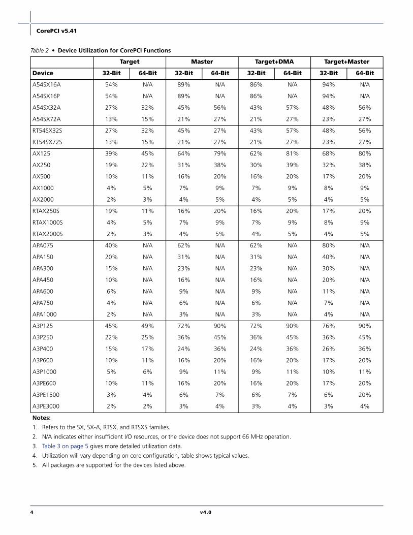
Table 2 • Device Utilization for CorePCI Functions
Target Master Target+DMA Target+Master
Device 32-Bit 64-Bit 32-Bit 64-Bit 32-Bit 64-Bit 32-Bit 64-Bit
A54SX16A 54% N/A 89% N/A 86% N/A 94% N/A
A54SX16P 54% N/A 89% N/A 86% N/A 94% N/A
A54SX32A 27% 32% 45% 56% 43% 57% 48% 56%
A54SX72A 13% 15% 21% 27% 21% 27% 23% 27%
RT54SX32S 27% 32% 45% 27% 43% 57% 48% 56%
RT54SX72S 13% 15% 21% 27% 21% 27% 23% 27%
AX125 39% 45% 64% 79% 62% 81% 68% 80%
AX250 19% 22% 31% 38% 30% 39% 32% 38%
AX500 10% 11% 16% 20% 16% 20% 17% 20%
AX1000 4% 5% 7% 9% 7% 9% 8% 9%
AX2000 2% 3% 4% 5% 4% 5% 4% 5%
RTAX250S 19% 11% 16% 20% 16% 20% 17% 20%
RTAX1000S 4% 5% 7% 9% 7% 9% 8% 9%
RTAX2000S 2% 3% 4% 5% 4% 5% 4% 5%
APA075 40% N/A 62% N/A 62% N/A 80% N/A
APA150 20% N/A 31% N/A 31% N/A 40% N/A
APA300 15% N/A 23% N/A 23% N/A 30% N/A
APA450 10% N/A 16% N/A 16% N/A 20% N/A
APA600 6% N/A 9% N/A 9% N/A 11% N/A
APA750 4% N/A 6% N/A 6% N/A 7% N/A
APA1000 2% N/A 3% N/A 3% N/A 4% N/A
A3P125 45% 49% 72% 90% 72% 90% 76% 90%
A3P250 22% 25% 36% 45% 36% 45% 36% 45%
A3P400 15% 17% 24% 36% 24% 36% 26% 36%
A3P600 10% 11% 16% 20% 16% 20% 17% 20%
A3P1000 5% 6% 9% 11% 9% 11% 10% 11%
A3PE600 10% 11% 16% 20% 16% 20% 17% 20%
A3PE1500 3% 4% 6% 7% 6% 7% 6% 20%
A3PE3000 2% 2% 3% 4% 3% 4% 3% 4%
Notes:
1. Refers to the SX, SX-A, RTSX, and RTSXS families.
2. N/A indicates either insufficient I/O resources, or the device does not support 66 MHz operation.
3. Table 3 on page 5 gives more detailed utilization data.
4. Utilization will vary depending on core configuration, table shows typical values.
5. All packages are supported for the devices listed above.
4 v4.0

CorePCI v5.41
Utilization StatisticsUtilization statistics are given in Table 2 on page 4.Table 3 gives a detailed breakdown of the actual gatecounts for each of the core variations and options listedin Table 3. The antifuse column indicates the typical Rand C module counts for the SX, SX-A, RTSX-S, andAxcelerator families. The Flash column indicates the tile
counts for the ProASICPLUS and ProASIC3/E families.These are typical numbers and will vary based on thesynthesis tools and constraints used. Each backendrequires different amounts of logic depending on thecomplexity of the controller. An SDRAM controller isincluded as an example.
Table 3 • Utilization Statistics for CorePCI
Function
Antifuse1ProASICPLUS
Flash2ProASIC3/E
Flash2
Sequential Combinatorial Total Tiles Tiles
32-Bit Target Controller 262 528 790 1218 1194
64-Bit Target Controller 350 560 910 N/A 1266
32-Bit Master Controller 480 810 1290 1900 1862
64-Bit Master Controller 600 1000 1600 N/A 2590
32-Bit Target+DMA Controller 400 850 1250 1904 1866
64-Bit Target+DMA Controller 554 1087 1641 N/A 2815
32-Bit Target/Master Controller 470 900 1370 2437 2389
64-Bit Target/Master Controller 570 1050 1620 N/A 2720
SDRAM Controller 70 130 200 230 225
BAR #1 Support 30 70 100 140 137
DMA Mapped into I/O3 30 90 120 120 117
Notes:
1. The sequential number is the R-module usage and the combinatorial number is the C-module usage.
2. Total number of tiles required.
3. Only applicable to Target+DMA functions.
Table 4 • Core I/O Requirements
Core
I/O Count
PCI
Backend Total
Minimum Standard* Minimum Standard*
32-Bit Target Controller 48 1 74 49 122
64-Bit Target Controller 87 1 113 88 200
32-Bit Master Controller 50 1 83 51 133
64-Bit Master Controller 89 1 122 90 211
32-Bit Target+DMA Controller 50 1 74 51 124
64-Bit Target+DMA Controller 89 1 113 90 202
32-Bit Target+Master Controller 50 1 83 51 133
64-Bit Target+Master Controller 89 1 122 90 211
Note: *Assumes all the backend I/O pins as listed in the data sheet are connected to I/O pins rather than to internal FPGA logic.
v4.0 5
CorePCI v5.41
CorePCI IP Functional Block DiagramCorePCI consists of six major functional blocks, shown inFigure 2 on page 7. These blocks are the DMA statemachine, the address phase state machine, thedataphase state machine, the datapath, parity, and theconfiguration block. All of the blocks shown are requiredto implement the Target+DMA and Target+Masterfunctions. For the Target-only core, the DMA statemachine is eliminated. For the Master-only core, theconfiguration block is not required. The DMA, address phase, and dataphase state machinescontrol the core’s outputs and also the dataflowbetween the PCI bus and the backend. The remainingmodules define the datapath logic for CorePCI.
DMA State MachineThe DMA state machine is responsible for obtainingMaster ownership of the PCI bus and launching a datatransfer by asserting FRAMEn. Once a burst transactionhas begun, the DMA state machine tracks the transfercount and terminates the burst by de-asserting theFRAMEn signal and releasing Master ownership of thePCI bus. In addition to basic Master control, the DMAmodule also implements the DMA support registers, PCIStart Address, RAM Start Address, and DMA Control.
Address Phase State MachineThe address phase state machine is responsible formonitoring the PCI bus and determining if a PCItransaction is targeting CorePCI. When a hit is detected,the DP_START/DP_START64 signals are activated, settingoff the dataphase machine and backend logic. Theaddress phase state machine also determines the cycletype and provides this information on the RD_CYC,WR_CYC, BAR0_MEM_CYC, BAR1_CYC, and CONFIG_CYCoutputs.
Dataphase State MachineThe dataphase state machine is responsible forcontrolling the PCI output signals and coordinating thedata transfers with the backend logic. When operatingas a Target, the PCI outputs are TRDYn, DEVSELn, andSTOPn. When operating as a Master, IRDYn is theprimary PCI output. Data transfers to the backend arecoordinated using the signals RD_BE_RDY, RD_BE_NOW,WR_BE_RDY, and WR_BE_NOW. The two "BE_RDY"inputs indicate that the backend is ready to transmit orreceive data. The "BE_NOW" signals are synchronousdata strobes and indicate that a data transfer will occuron the next rising edge of the clock. The dataphase statemachine also drives the DP_DONE output active at theend of the PCI transfer.
DatapathThe datapath module provides the steering and registersfor the data between the PCI bus and the backend.Additionally, the datapath contains the address countersand increments the value after each data transaction.
ParityThe parity block generates and checks parity on the PCIbus.
Configuration The configuration block contains the configurationregister file for the Target controller. These registersinclude the ID, status, control, and the base addressregisters. The core implements a single function Type 0configuration space.
Data Transactions CorePCI is designed to be fully compliant for all transfertypes, including both single DWORD and bursttransactions. Burst transfers can operate with eitherzero, one, or more wait states. Normally, CorePCI willburst data with zero wait states; however, for slowresponse peripherals, CorePCI can insert wait statesunder the control of the backend. During Targetoperation, wait states are inserted by driving TRDYnhigh. During Master operation, CorePCI drives IRDYnhigh to insert wait states.
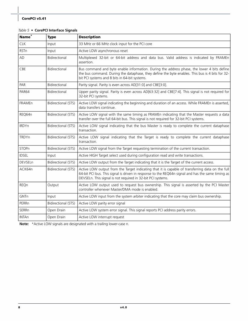
I/O Signal DescriptionsThe PCI and backend signals for CorePCI are defined inTable 5 on page 8 and Table 6 on page 9. For thepurposes of this data sheet, the following signal typedefinitions are used:
• Input: Standard input-only signal.
• Output: Standard active driver that drivescontinuously.
• Tristate Output: Standard active driver that can betristated.
• Bidirectional (referred to as t/s in the PCIspecification): A combination input and t/s outputpin.
• Sustained Tristate (s/t/s in the PCI specification): Aterm used to describe either bidirectional or t/soutput pins. The STS term indicates that the signalshould always be driven to a logic '1' before thepin is tristated.
• Open Drain: Drive to '0' only output. A pull-up isrequired to sustain the high-impedance state to alogic '1' and is provided by the PCI backplane.
6 v4.0

CorePCI v5.41
For a complete list of signal descriptions, refer to Table 5 on page 8 and Table 6 on page 9.Figure 2 • CorePCI Block Diagram
IRDYn
STOPn
DEVSELn
TRDYn
SERRn
IDSEL
AD
PAR
CBE
PERRn
INTAn
FRAMEn
REQn
GNTn
CLK
RSTn
PCI Bus Back-EndInterface
BE_REQBE_GNT
DP_START
DP_DONE
MEM_ADD[23:0]RD_CYCWR_CYCBAR0_MEM_CYCBAR1_CYCCONFIG_CYC
BE_RD_RDYRD_BE_NOW
BE_WR_RDYWR_BE_NOW[3:0]
EXT_INTn
DP_START64
RD_BE_NOW64
WR_BE_NOW64[3:0]
ERROR
CLK_OUT
DMA_GNTSTALL_MASTER
MEM_DOUTMEM_DINMEM_DEN
ERRORBUSY
EXT_INTNCS_CONTROLNRD_CONTROLNWR_CONTROLNMASTER_BEMASTER_BE64
BUSY_MASTERAddress PhaseState Machine
Configuration
DMA Controllerand
Register File
Datapath
Parity
Block
DataphaseState Machine
v4.0 7
CorePCI v5.41
Table 5 • CorePCI Interface Signals
Name* Type Description
CLK Input 33 MHz or 66 MHz clock input for the PCI core
RSTn Input Active LOW asynchronous reset
AD Bidirectional Multiplexed 32-bit or 64-bit address and data bus. Valid address is indicated by FRAMEnassertion.
CBE Bidirectional Bus command and byte enable information. During the address phase, the lower 4 bits definethe bus command. During the dataphase, they define the byte enables. This bus is 4 bits for 32-bit PCI systems and 8 bits in 64-bit systems.
PAR Bidirectional Parity signal. Parity is even across AD[31:0] and CBE[3:0].
PAR64 Bidirectional Upper parity signal. Parity is even across AD[63:32] and CBE[7:4]. This signal is not required for32-bit PCI systems.
FRAMEn Bidirectional (STS) Active LOW signal indicating the beginning and duration of an access. While FRAMEn is asserted,data transfers continue.
REQ64n Bidirectional (STS) Active LOW signal with the same timing as FRAMEn indicating that the Master requests a datatransfer over the full 64-bit bus. This signal is not required for 32-bit PCI systems.
IRDYn Bidirectional (STS) Active LOW signal indicating that the bus Master is ready to complete the current dataphasetransaction.
TRDYn Bidirectional (STS) Active LOW signal indicating that the Target is ready to complete the current dataphasetransaction.
STOPn Bidirectional (STS) Active LOW signal from the Target requesting termination of the current transaction.
IDSEL Input Active HIGH Target select used during configuration read and write transactions.
DEVSELn Bidirectional (STS) Active LOW output from the Target indicating that it is the Target of the current access.
ACK64n Bidirectional (STS) Active LOW output from the Target indicating that it is capable of transferring data on the full64-bit PCI bus. This signal is driven in response to the REQ64n signal and has the same timing asDEVSELn. This signal is not required in 32-bit PCI systems.
REQn Output Active LOW output used to request bus ownership. This signal is asserted by the PCI Mastercontroller whenever Master/DMA mode is enabled.
GNTn Input Active LOW input from the system arbiter indicating that the core may claim bus ownership.
PERRn Bidirectional (STS) Active LOW parity error signal
SERRn Open Drain Active LOW system error signal. This signal reports PCI address parity errors.
INTAn Open Drain Active LOW interrupt request
Note: *Active LOW signals are designated with a trailing lower-case n.
8 v4.0

CorePCI v5.41
Table 6 • CorePCI Backend Interface Signal
Name1,2 Type Description
CLK_OUT Output Clock Output. The core uses an internal clock buffer, this is buffered version of the clock andshould be used for clocking any other logic in the FPGA that is clocked by the PCI clock.
BAR0_MEM_CYC Output Active high signal indicating a transaction to the memory space defined in the base addressregister zero (BAR0) located at 10H in Configuration Header Space.
BAR1_CYC Output Active high signal indicating a transaction to the optional memory or I/O space defined in baseaddress register one (BAR1) located at 14H in Configuration Header Space.
CONFIG_CYC Output Active high signal indicating a transaction to configuration space.
RD_CYC Output Active high signal indicating a read transaction from the backend.
WR_CYC Output Active high signal indicating a write transaction to the backend.
MEM_DIN Input DWORD aligned 32- or 64-bit databus input
MEM_DOUT Output DWORD aligned 32- or 64-bit databus output
MEM_DATA_DEN Output Active high data enable for MEM_DOUT, lower 32-bit. This is intended as an output enable ifMEM_DIN and MEM_DOUT are connected to bi-directional pads.
MEM_DATA_DEN64 Output Active high data enable for MEM_DOUT, upper 32-bit. This is intended as an output enable ifMEM_DIN and MEM_DOUT are connected to bi-directional pads.
MEM_ADD[N:0]3 Output DWORD aligned memory address bus where N is defined by the variable MADDR_WIDTH.Since the PCI address is byte aligned, a 2-bit shift of the address is performed and PCI addressbits 0 and 1 are discarded. For example, a 1 Mbyte memory requires 20 address bits touniquely address each byte or 18 address bits to uniquely address each DWORD. A PCI addressof 'CCCCC'h would translate to '33333'h on the backend. For writes, individual bytes arequalified with the 4-bit WR_BE_NOW bus. All reads are assumed to be full DWORDS.
DP_START
DP_START64
Output DP_START is an active high pulse indicating that a PCI transaction to the backend is beginning.If the transfer is 64-bit, then DP_START64 will be asserted at the same time as DP_START.
DP_DONE Output Active high pulse indicating that a successful PCI transaction to the backend has finished.
RD_BE_NOW
RD_BE_NOW64
Output Active High Synchronized Read Strobe. When active high, these signals indicate that the PCIcontroller will read data on the MEM_DATA bus on the next rising clock edge. These signalsare active whenever both the backend (as indicated by RD_BE_RDY) and the PCI bus (asindicated by IRDYn) are ready to transmit data. The RD_BE_NOW indicates a write to the lower32 bits of data and the RD_BE_NOW64 indicates a read from the upper 32 bits of data.Function of these signals are impacted by the PIPE_FULL_CNT bus (Figure 15).
RD_BE_RDY Input Active high signal indicating that the backend is ready to send data to the Target interface. Ifthe ready signal does not become active within the limits defined by the PCI bus, then adisconnect without data will be initiated.
Notes:
1. Active LOW signals are designated with a trailing lower-case n.
2. Signals ending in "CYC" become valid as the same cycle DP_START is active and will remain valid throughout the current cycle (untilDP_DONE is asserted).
3. MADDR_WIDTH is defined in Table 22 on page 20.
4. All inputs should be synchronous to the PCI clock.
v4.0 9
CorePCI v5.41
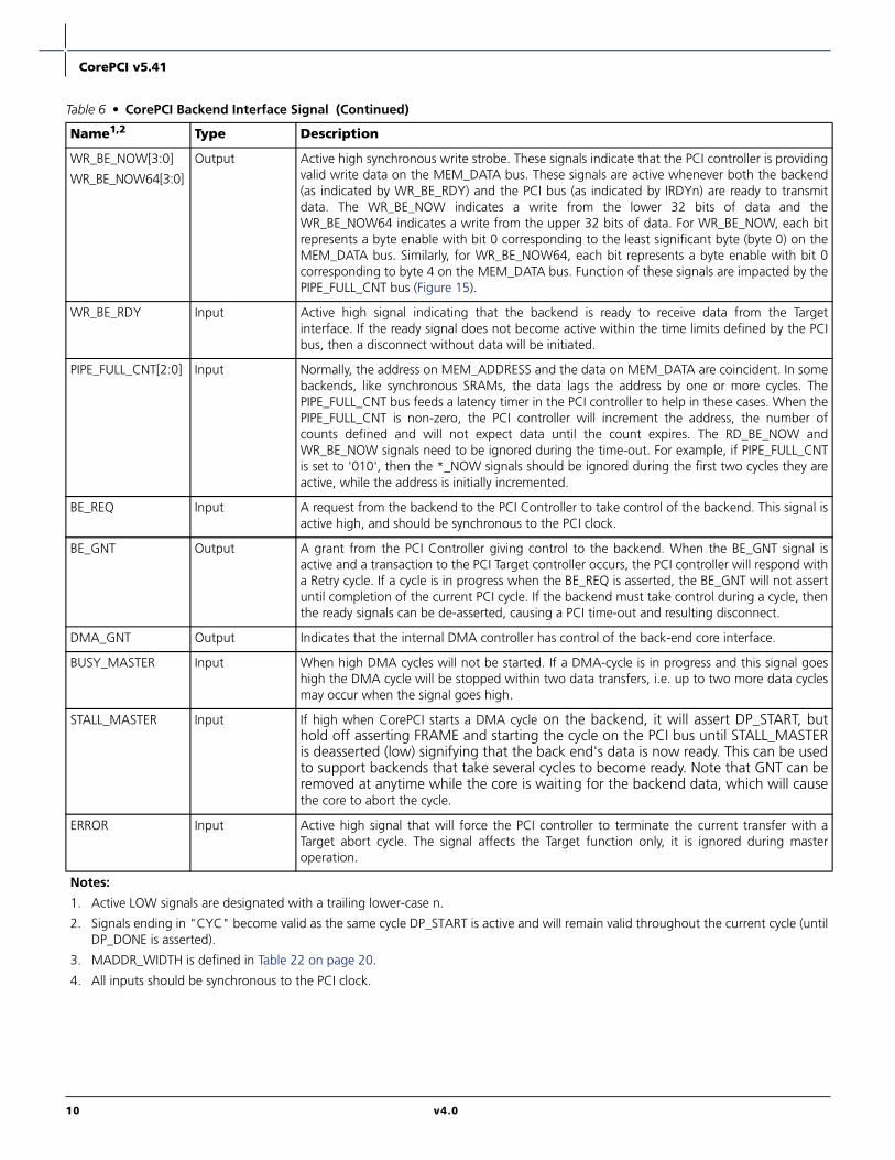
WR_BE_NOW[3:0]
WR_BE_NOW64[3:0]
Output Active high synchronous write strobe. These signals indicate that the PCI controller is providingvalid write data on the MEM_DATA bus. These signals are active whenever both the backend(as indicated by WR_BE_RDY) and the PCI bus (as indicated by IRDYn) are ready to transmitdata. The WR_BE_NOW indicates a write from the lower 32 bits of data and theWR_BE_NOW64 indicates a write from the upper 32 bits of data. For WR_BE_NOW, each bitrepresents a byte enable with bit 0 corresponding to the least significant byte (byte 0) on theMEM_DATA bus. Similarly, for WR_BE_NOW64, each bit represents a byte enable with bit 0corresponding to byte 4 on the MEM_DATA bus. Function of these signals are impacted by thePIPE_FULL_CNT bus (Figure 15).
WR_BE_RDY Input Active high signal indicating that the backend is ready to receive data from the Targetinterface. If the ready signal does not become active within the time limits defined by the PCIbus, then a disconnect without data will be initiated.
PIPE_FULL_CNT[2:0] Input Normally, the address on MEM_ADDRESS and the data on MEM_DATA are coincident. In somebackends, like synchronous SRAMs, the data lags the address by one or more cycles. ThePIPE_FULL_CNT bus feeds a latency timer in the PCI controller to help in these cases. When thePIPE_FULL_CNT is non-zero, the PCI controller will increment the address, the number ofcounts defined and will not expect data until the count expires. The RD_BE_NOW andWR_BE_NOW signals need to be ignored during the time-out. For example, if PIPE_FULL_CNTis set to '010', then the *_NOW signals should be ignored during the first two cycles they areactive, while the address is initially incremented.
BE_REQ Input A request from the backend to the PCI Controller to take control of the backend. This signal isactive high, and should be synchronous to the PCI clock.
BE_GNT Output A grant from the PCI Controller giving control to the backend. When the BE_GNT signal isactive and a transaction to the PCI Target controller occurs, the PCI controller will respond witha Retry cycle. If a cycle is in progress when the BE_REQ is asserted, the BE_GNT will not assertuntil completion of the current PCI cycle. If the backend must take control during a cycle, thenthe ready signals can be de-asserted, causing a PCI time-out and resulting disconnect.
DMA_GNT Output Indicates that the internal DMA controller has control of the back-end core interface.
BUSY_MASTER Input When high DMA cycles will not be started. If a DMA-cycle is in progress and this signal goeshigh the DMA cycle will be stopped within two data transfers, i.e. up to two more data cyclesmay occur when the signal goes high.
STALL_MASTER Input If high when CorePCI starts a DMA cycle on the backend, it will assert DP_START, buthold off asserting FRAME and starting the cycle on the PCI bus until STALL_MASTERis deasserted (low) signifying that the back end's data is now ready. This can be usedto support backends that take several cycles to become ready. Note that GNT can beremoved at anytime while the core is waiting for the backend data, which will causethe core to abort the cycle.
ERROR Input Active high signal that will force the PCI controller to terminate the current transfer with aTarget abort cycle. The signal affects the Target function only, it is ignored during masteroperation.
Table 6 • CorePCI Backend Interface Signal (Continued)
Name1,2 Type Description
Notes:
1. Active LOW signals are designated with a trailing lower-case n.
2. Signals ending in "CYC" become valid as the same cycle DP_START is active and will remain valid throughout the current cycle (untilDP_DONE is asserted).
3. MADDR_WIDTH is defined in Table 22 on page 20.
4. All inputs should be synchronous to the PCI clock.
10 v4.0

CorePCI v5.41
BUSY Input Active high signal indicating that the backend controller cannot complete the current transfer.When BUSY is active at the beginning of a transfer, the Target controller will perform a retrycycle. If BUSY is activated after some data has been transferred, the Target controller willperform a disconnect cycle, either with or without data. The signal affects the Target functiononly, it is ignored during master operations.
EXT_INTn Input Active low interrupt from the backend. When PCI interrupts are enabled, this should cause anINTAn signal to be asserted.
CS_CONTROLn Input Active low chip select to the DMA registers (Master and Target+Master functions).
RD_CONTROLn Input Active low synchronous read enable for the DMA registers (Master and Target+Masterfunctions only).
WR_CONTROLn Input Active low synchronous write enable for the DMA registers (Master and Target+Masterfunctions only).
CONTROL_ADD[1:0] Input Two-bit address used to address the DMA registers from the backend (Master andTarget+Master functions only).
MASTER_BE[3:0] Input Active low-byte enable inputs used during master transfer to drive the lower CBE lines.
MASTER_BE64[3:0] Input Active low-byte enable inputs used during master transfer to drive the upper CBE lines
Table 6 • CorePCI Backend Interface Signal (Continued)
Name1,2 Type Description
Notes:
1. Active LOW signals are designated with a trailing lower-case n.
2. Signals ending in "CYC" become valid as the same cycle DP_START is active and will remain valid throughout the current cycle (untilDP_DONE is asserted).
3. MADDR_WIDTH is defined in Table 22 on page 20.
4. All inputs should be synchronous to the PCI clock.
v4.0 11

CorePCI v5.41
CorePCI Target FunctionCorePCI Target function acts like a slave on the PCI bus.The Target controller monitors the bus and checks forhits to either configuration space or to the address spacedefined in its base address registers (BARs). When a hit isdetected, the Target controller notifies the backend andthen acts to control the flow of data between the PCI busand the backend.
Supported Target CommandsTable 7 on page 12 lists the PCI commands supported inthe current CorePCI Target implementation. If required,I/O support, and thus I/O commands, can be eliminatedfrom the design by setting the appropriatecustomization options.
I/O Read (0010) and Write (0011)The I/O read command is used to read data mapped intoI/O address space. CorePCI will not check to verify theconsistency of the address and byte enables. This and anyadditional error checking is left for implementation bythe user. The I/O write command is used to write datamapped into I/O address space. In this case, the write isqualified by the byte enables. The default I/O space sizeis 256 bytes.
Memory Read (0110) and Write (0111)The memory read and write commands are used to readdata in memory-mapped address space. The baselinememory core supports 4 megabytes for the 32-bit coreand 8 megabytes for the 64-bit core, which can belocated anywhere in 32-bit address space. The memorysize may be set to any value using the MADDR_WIDTHcustomization constant.
Configuration Read (1010) and Write (1011)The configuration read command is used to read theconfiguration space of each device. The configurationwrite command is employed to write information intothe configuration space. The device is selected if its IDSELsignal is asserted and AD[1:0] are '00'b. Additionaladdress bits are defined as follows:
• AD[7:2] contain one of 64 DWORD addresses forthe configuration registers.
• AD[10:8] indicate which device of a multi-functionagent is addressed. The core does not supportmulti-function devices and these bits should be'000'b.
• AD[31:11] are "don’t cares."
Supported Cycle TypesCorePCI Target will perform either single DWORD orburst transactions depending on the request from thesystem Master. If the backend is unable to deliver data,the Target will respond with either a PCI Retry orDisconnect, either with or without data. If the systemMaster requests a transfer that the backend is not ableto perform, a Target abort can be initiated by thebackend.
Target Configuration SpaceThe PCI specification requires a 64-byte configurationspace (header) to define various attributes of the PCITarget, as shown in Table 8 on page 13. All registersshown in bold are implemented, including the two baseaddress registers. None of the remaining registers areincluded in the baseline implementation and will returnzeroes when read.
In the Target-only function, one additional configurationregister, 48h, is used to define backend interrupt controland status. For other functions, this information iscontained in the DMA control register.
Table 7 • Supported PCI Target Commands
C/BE[3:0] Command Type Supported
0000 Interrupt Acknowledge No
0001 Special Cycle No
0010 I/O Read Yes
0011 I/O Write Yes
0100 Reserved –
0101 Reserved –
0110 Memory Read Yes
0111 Memory Write Yes
1000 Reserved –
1001 Reserved –
1010 Configuration Read Yes
1011 Configuration Write Yes
1100 Memory Read Multiple Yes
1101 Dual Address Cycle No
1110 Memory Read Line Yes
1111 Memory Write and Invalidate No
12 v4.0

CorePCI v5.41
Read-Only Configuration RegistersThe read-only registers listed in Table 8 on page 13 havedefault values, but should be modified by the designer.See the PCI specification for setting these values:
• Vendor ID
• Device ID
• Revision ID
• Class Code
• Subsystem ID
• Subsystem Vendor ID
The header type register is also read-only, but should notbe modified (pre-set to a constant value of '00h'). TheCapability Pointer is included when the HOT_SWAP_ENcustomization constant is set to '1'b. See Table 13 onpage 16 for more information.
Read/Write Configuration RegistersThe following registers have at least one bit that is bothread and write capable. For a complete description, referto the appropriate table.
• "Command Register (04h)" (Table 9 on page 14)
• " Status Register (06h)" (Table 10 on page 14)
• "Memory Base Address Register Bit Definition(Locations 10h or 14h)" (Table 11 on page 16)
• "I/O Base Address Register Bit Definitions(Location 14h Only)" (Table 12 on page 16)
• "Interrupt Register (3Ch)" (Table 14 on page 16)
• "Interrupt Control/Status Register (48h)" (Table 15on page 16)
• "Optional Hot-Swap Register (80h)" (Table 16 onpage 16)
Table 8 • PCI Configuration Header
31–24 23–16 15–8 7–0 Address
Device ID Vendor ID 00h
Status Command 04h
Class Code Revision ID 08h
BIST Header Type Latency Timer Cache Line Size 0Ch
Base Address #0 (Memory Location for Baseline Target) 10h
Base Address #1 (Optional Memory or I/O) 14h
Base Address #2 (Optional I/O for DMA Register Mapping) 18h
Base Address #3 1Ch
Base Address #4 20h
Base Address #5 24h
CardBus CIS Pointer 28h
Subsystem ID Subsystem Vendor ID 2Ch
Expansion ROM Base Address 30h
Reserved Capabilities Pointer 34h
Reserved 38h
Max_Lat Min_Gnt Interrupt Pin Interrupt Line 3Ch
Interrupt Control/Status Register 48h
Hot-Swap Register (optional) 80h
v4.0 13

CorePCI v5.41
Table 9 • Command Register (04h)
Bit Type Description
0 RW I/O Space
A value of '0' disables the device’s response to I/O space addresses. Set to '0' after reset.
1 RW Memory Space
A value of '0' disables the device’s response to memory space addresses. Set to '0' after reset.
2 RW Bus Master
When set to a '1' this bit enables the macro to behave as a PCI bus Master. For Target-onlyimplementation, this bit is read-only and is set to '0'.
3 RO Special Cycles
No response to special cycles. It is set to '0'.
4 RO Memory write and invalidate enable
Memory write and invalidate not supported. It is set to '0'.
5 RO VGA Palette Snoop
Assumes non-VGA peripheral. It is set to '0'.
6 RW Parity Error Response
When '0' the device ignores parity errors. When '1' normal parity checking is performed. Set to '0'after reset.
7 RO Wait Cycle Control
No data-stepping supported. It is set to '0'.
8 RW SERRn Enable
When '0' the SERRn driver is disabled. It is set to '0' after reset.
9 RO Fast Back-to-Back Enable
Set to '0'. Only fast back-to-back transactions to same agent are allowed.
10 RW Interrupt Disable
When set this prevents the Core from asserting its INTAn output. This bit is set to '0' after reset.
15–11 RO Reserved and set to all '0's.
Note: RW = Read and writeRO = Read only
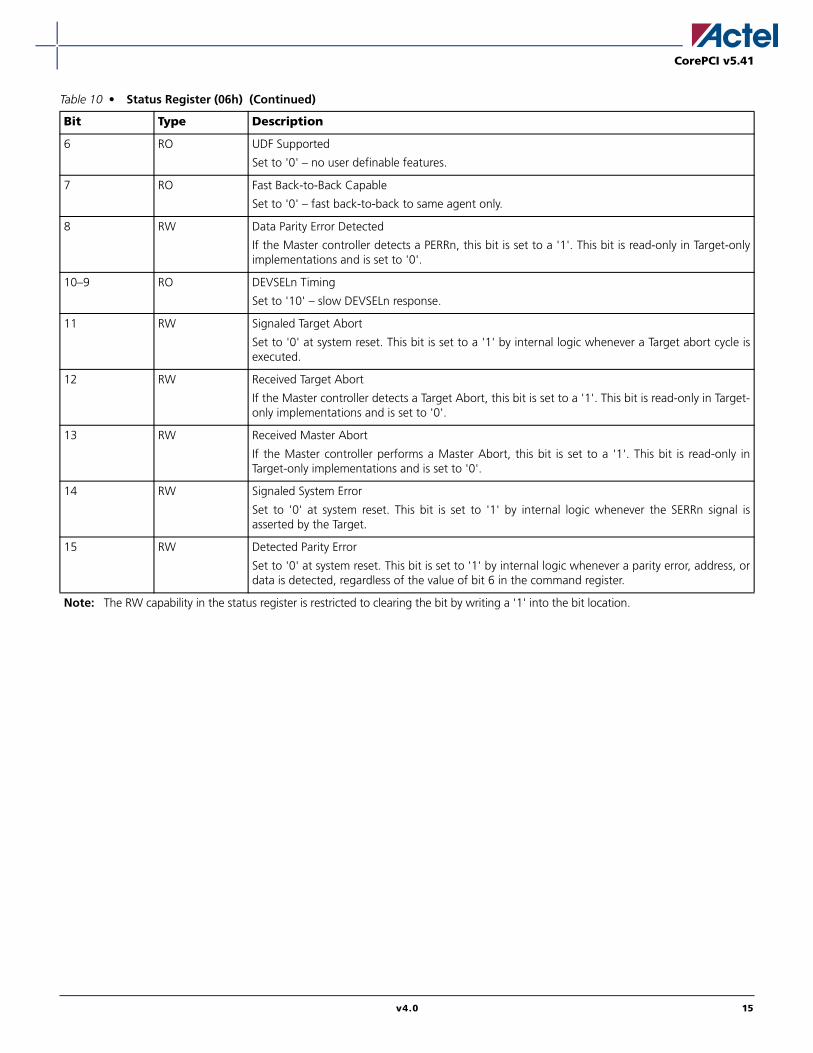
Table 10 • Status Register (06h)
Bit Type Description
2–0 RO Reserved—set to '000'b.
3 RO Interrupt Status
This bit reflects the status of the INTAn output.
4 RO Capabilities List
When the HOT_SWAP_EN customization constant is set to a '1', the bit is set to a '1'; otherwise, itis set to '0'.
5 RO 66 MHz Capable
Should be set to '1' to indicate a 66 MHz Target, or '0' to indicate a 33 MHz Target. The valuedepends on the MHZ_66 customization constant.
Note: The RW capability in the status register is restricted to clearing the bit by writing a '1' into the bit location.
14 v4.0
CorePCI v5.41
6 RO UDF Supported
Set to '0' – no user definable features.
7 RO Fast Back-to-Back Capable
Set to '0' – fast back-to-back to same agent only.
8 RW Data Parity Error Detected
If the Master controller detects a PERRn, this bit is set to a '1'. This bit is read-only in Target-onlyimplementations and is set to '0'.
10–9 RO DEVSELn Timing
Set to '10' – slow DEVSELn response.
11 RW Signaled Target Abort
Set to '0' at system reset. This bit is set to a '1' by internal logic whenever a Target abort cycle isexecuted.
12 RW Received Target Abort
If the Master controller detects a Target Abort, this bit is set to a '1'. This bit is read-only in Target-only implementations and is set to '0'.
13 RW Received Master Abort
If the Master controller performs a Master Abort, this bit is set to a '1'. This bit is read-only inTarget-only implementations and is set to '0'.
14 RW Signaled System Error
Set to '0' at system reset. This bit is set to '1' by internal logic whenever the SERRn signal isasserted by the Target.
15 RW Detected Parity Error
Set to '0' at system reset. This bit is set to '1' by internal logic whenever a parity error, address, ordata is detected, regardless of the value of bit 6 in the command register.
Table 10 • Status Register (06h) (Continued)
Bit Type Description
Note: The RW capability in the status register is restricted to clearing the bit by writing a '1' into the bit location.
v4.0 15

CorePCI v5.41
Table 11 • Memory Base Address Register Bit Definition (Locations 10h or 14h)
Bit Type Description
0 RO Set to '0' to indicate memory space.
2–1 RO Set to '00' to indicate mapping into any 32-bitaddress space.
3 RO Set to a '1' Indicating prefetch allowed onreads.
23–4 RO Indicates a 16 MB address space. It is set to all'0's.
31–24 RW Programmable location for 16 MB addressspace. To determine a hit, these bits must becompared to PCI address bits 31–24.
Note: The description for bit values 31–24 and 23–4 will varydepending on the actual memory size defined in thecustomization options. See "Customization Options" onpage 19 for more information.
Table 12 • I/O Base Address Register Bit Definitions (Location 14h Only)
Bit Type Description
0 RO Set to '1' to indicate I/O space.
1 RO Reserved. It is set to '0'.
7–2 RO 256-byte I/O space for this peripheral. It is setto all '0's.
31–8 RW Programmable address for this peripheral’s I/Ospace. To determine a hit, these bits must becompared to PCI address bits 31–8.
Note: The description for bit values 31–8 and 7–2 will varydepending on the actual memory size defined in thecustomization options. See "Customization Options" onpage 19 for more information.
Table 13 • Capabilities Pointer (34h)
Bit Type Description
7–0 RO Set to '10000000'b when the customizationconstant, HOT_SWAP_EN, is set to a '1';otherwise, it is all zeroes.
31–8 RW Reserved. It is set to '0'.
Note: This register is not required if hot-swap is not enabled.See "Customization Options" on page 19 for moreinformation.
Table 14 • Interrupt Register (3Ch)
Bit Type Description
7–0 RW Required read/write register. This register hasno impact on internal logic.
15–8 RO Set to '00000001'b to indicate INTAn.
Table 15 • Interrupt Control/Status Register (48h)
Bit Type Description
7–0 RO Reserved. It is set to all zeroes.
8 RW A '1' in this bit indicates an active externalinterrupt condition (assertion of EXT_INTn). The user can clear it by writing a '1' to the bitposition. It is set to '0' after reset.
9 RW Writing a '1' to this bit enables support for theexternal interrupt signal. Writing a '0' to thisbit disables external interrupt support.
31–10 RO Reserved. It is set to '0'.
Table 16 • Optional Hot-Swap Register (80h)
Bit Type Description
7–0 RO Reserved. It is set to all zeroes.
8 RO Reserved. It is set to '0'.
9 RW ENUM# Signal Mask.
10 RO Reserved. It is set to '0'.
11 RW LED ON/OFF. When set to a '1', this bit is usedto drive a blue LED indicating that it is safe toextract the card.
13–12 RO Reserved. It is set to '0'.
14 RW ENUM# Insertion Status.
15 RW ENUM# Insertion Status.
23–16 RO The next item located in the capabilities list.Set to '0' in the baseline core.
31–24 RO Set to '06'h to indicate hot-swap capability.
16 v4.0

CorePCI v5.41
CorePCI Master FunctionThe Master function in CorePCI is designed to performthe following:
• Arbitrate for the PCI bus
• Initiate an access by asserting FRAMEn andproviding the address and command
• Pass dataflow control to the Target controller
• End the transfer when the DMA count has beenexhausted by de-asserting FRAMEn
Supported Master CommandsCorePCI Master controller is capable of performingconfiguration, I/O, memory, and interrupt acknowledgecycles. Data transfers can be up to 4kb. However,configuration and I/O commands are typically limited toa single DWORD.
The Master controller will attempt to complete thetransfer in a single burst unless the maximum burstlength bits are set in the control register. If the addressedTarget is unable to complete the transfer and performs aRetry or Disconnect, the Master control will restart thetransfer and continue from the last known good transfer.If a Target does not respond (no DEVSELn asserted) orresponds with Target Abort cycle, the Master controllerwill abort the current transaction and report it as anerror in the control register. The supported CorePCIMaster commands are listed in Table 17.
Master RegistersThere are three registers used to control the function ofCorePCI Master. The first register is the 32-bit PCI addressregister. The second register is the 32-bit RAM orbackend address register. These two registers provide thesource/destination addressing for all data transfers. A 32-bit control register defines the type, length, and status ofa Master transfer. These registers are cleared on reset.They are defined in detail in Table 18 and Table 19 onthis page, and Table 20 on page 18.
Table 17 • Supported CorePCI Master Commands
CBE[3:0] Command Type
0000 Interrupt Acknowledge Cycle
0010 I/O Read
0011 I/O Write
0110 Memory Read
0111 Memory Write
1010 Configuration Read
1011 Configuration Write
Table 18 • PCI Start Address
Bit Type Description
1–0 RO Set to '00'b. PCI transfers must be on aDWORD boundary.
31–2 RW PCI Start Address
This location will increment during the DMAtransfer when the DMA_CNT_ENcustomization constant is set to a '1'.Otherwise at the end of a transfer, thisregister value will hold the initial startingaddress.
Table 17 • Supported CorePCI Master Commands
CBE[3:0] Command Type
Table 19 • RAM Start Address
Bit Type Description
1–0 RO Set to '00'b. PCI transfers must be on a DWORD boundary.
23–2 RW RAM Start Address
This location will increment during the DMA transfer when the DMA_CNT_EN customizationconstant is set to a '1'. Otherwise at the end of a transfer, this register value will hold the initialstarting address.
31–24 RO Set to all zeros.
Note: The description for bit values 31–24 and 23–2 will vary depending on the actual memory size defined in the customization options.See "Customization Options" on page 19 for more information. For this case, MADDR_WIDTH is set to 24.
v4.0 17
CorePCI v5.41
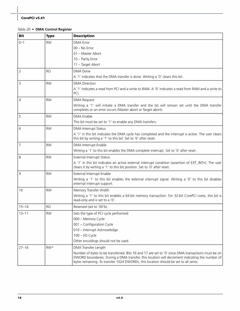
Table 20 • DMA Control Register
Bit Type Description
0–1 RW DMA Error
00 – No Error
01 – Master Abort
10 – Parity Error
11 – Target Abort
2 RO DMA Done
A '1' indicates that the DMA transfer is done. Writing a '0' clears this bit.
3 RW DMA Direction
A '1' indicates a read from PCI and a write to RAM. A '0' indicates a read from RAM and a write toPCI.
4 RW DMA Request
Writing a '1' will initiate a DMA transfer and the bit will remain set until the DMA transfercompletes or an error occurs (Master abort or Target abort).
5 RW DMA Enable
This bit must be set to '1' to enable any DMA transfers.
6 RW DMA Interrupt Status
A '1' in this bit indicates the DMA cycle has completed and the interrupt is active. The user clearsthis bit by writing a '1' to this bit. Set to '0' after reset.
7 RW DMA Interrupt Enable
Writing a '1' to this bit enables the DMA complete interrupt. Set to '0' after reset.
8 RW External Interrupt Status
A '1' in this bit indicates an active external interrupt condition (assertion of EXT_INTn). The userclears it by writing a '1' to this bit position. Set to '0' after reset.
9 RW External Interrupt Enable
Writing a '1' to this bit enables the external interrupt signal. Writing a '0' to this bit disablesexternal interrupt support.
10 RW Memory Transfer Width
Writing a '1' to this bit enables a 64-bit memory transaction. For 32-bit CorePCI cores, this bit isread-only and is set to a '0'.
15–14 RO Reserved (set to '00'b).
13–11 RW Sets the type of PCI cycle performed:
000 – Memory Cycle
001 – Configuration Cycle
010 – Interrupt Acknowledge
100 – I/O Cycle
Other encodings should not be used.
27–16 RW* DMA Transfer Length
Number of bytes to be transferred. Bits 16 and 17 are set to '0' since DMA transactions must be onDWORD boundaries. During a DMA transfer, this location will decrement indicating the number ofbytes remaining. To transfer 1024 DWORDs, this location should be set to all zeros.
18 v4.0
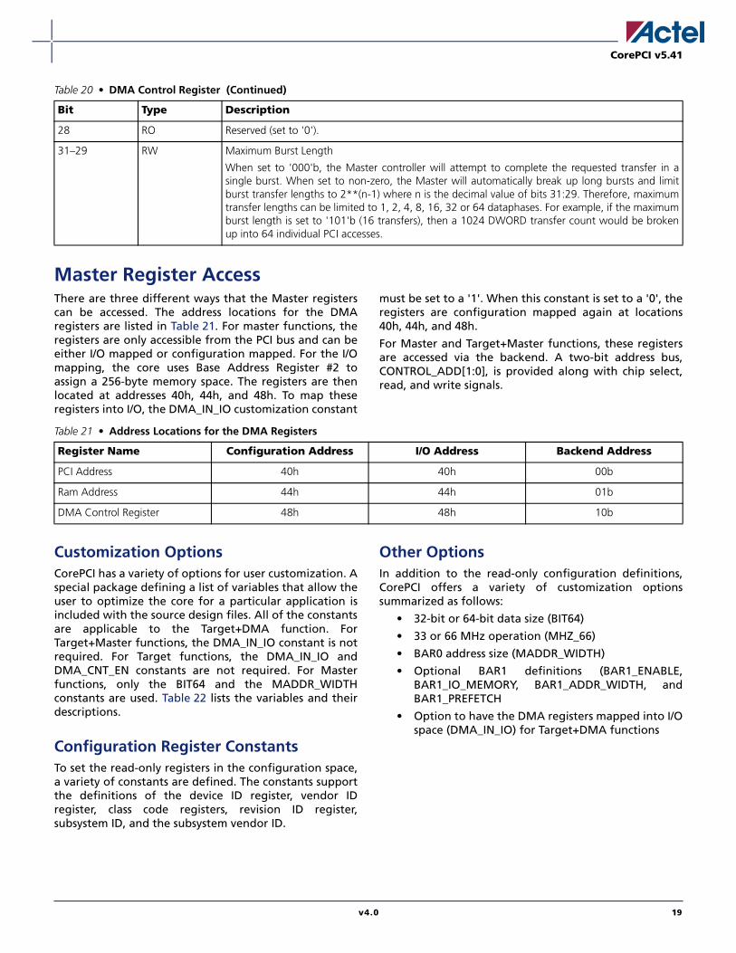
CorePCI v5.41
Master Register AccessThere are three different ways that the Master registerscan be accessed. The address locations for the DMAregisters are listed in Table 21. For master functions, theregisters are only accessible from the PCI bus and can beeither I/O mapped or configuration mapped. For the I/Omapping, the core uses Base Address Register #2 toassign a 256-byte memory space. The registers are thenlocated at addresses 40h, 44h, and 48h. To map theseregisters into I/O, the DMA_IN_IO customization constant
must be set to a '1'. When this constant is set to a '0', theregisters are configuration mapped again at locations40h, 44h, and 48h.
For Master and Target+Master functions, these registersare accessed via the backend. A two-bit address bus,CONTROL_ADD[1:0], is provided along with chip select,read, and write signals.
Customization OptionsCorePCI has a variety of options for user customization. Aspecial package defining a list of variables that allow theuser to optimize the core for a particular application isincluded with the source design files. All of the constantsare applicable to the Target+DMA function. ForTarget+Master functions, the DMA_IN_IO constant is notrequired. For Target functions, the DMA_IN_IO andDMA_CNT_EN constants are not required. For Masterfunctions, only the BIT64 and the MADDR_WIDTHconstants are used. Table 22 lists the variables and theirdescriptions.
Configuration Register ConstantsTo set the read-only registers in the configuration space,a variety of constants are defined. The constants supportthe definitions of the device ID register, vendor IDregister, class code registers, revision ID register,subsystem ID, and the subsystem vendor ID.
Other Options In addition to the read-only configuration definitions,CorePCI offers a variety of customization optionssummarized as follows:
• 32-bit or 64-bit data size (BIT64)
• 33 or 66 MHz operation (MHZ_66)
• BAR0 address size (MADDR_WIDTH)
• Optional BAR1 definitions (BAR1_ENABLE,BAR1_IO_MEMORY, BAR1_ADDR_WIDTH, andBAR1_PREFETCH
• Option to have the DMA registers mapped into I/Ospace (DMA_IN_IO) for Target+DMA functions
28 RO Reserved (set to '0').
31–29 RW Maximum Burst Length
When set to '000'b, the Master controller will attempt to complete the requested transfer in asingle burst. When set to non-zero, the Master will automatically break up long bursts and limitburst transfer lengths to 2**(n-1) where n is the decimal value of bits 31:29. Therefore, maximumtransfer lengths can be limited to 1, 2, 4, 8, 16, 32 or 64 dataphases. For example, if the maximumburst length is set to '101'b (16 transfers), then a 1024 DWORD transfer count would be brokenup into 64 individual PCI accesses.
Table 20 • DMA Control Register (Continued)
Bit Type Description
Table 21 • Address Locations for the DMA Registers
Register Name Configuration Address I/O Address Backend Address
PCI Address 40h 40h 00b
Ram Address 44h 44h 01b
DMA Control Register 48h 48h 10b
v4.0 19
CorePCI v5.41
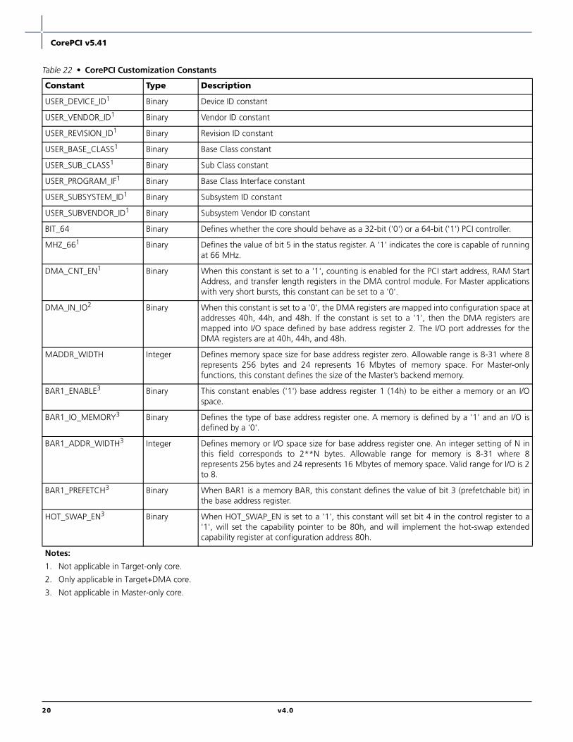
Table 22 • CorePCI Customization Constants
Constant Type Description
USER_DEVICE_ID1 Binary Device ID constant
USER_VENDOR_ID1 Binary Vendor ID constant
USER_REVISION_ID1 Binary Revision ID constant
USER_BASE_CLASS1 Binary Base Class constant
USER_SUB_CLASS1 Binary Sub Class constant
USER_PROGRAM_IF1 Binary Base Class Interface constant
USER_SUBSYSTEM_ID1 Binary Subsystem ID constant
USER_SUBVENDOR_ID1 Binary Subsystem Vendor ID constant
BIT_64 Binary Defines whether the core should behave as a 32-bit ('0') or a 64-bit ('1') PCI controller.
MHZ_661 Binary Defines the value of bit 5 in the status register. A '1' indicates the core is capable of runningat 66 MHz.
DMA_CNT_EN1 Binary When this constant is set to a '1', counting is enabled for the PCI start address, RAM StartAddress, and transfer length registers in the DMA control module. For Master applicationswith very short bursts, this constant can be set to a '0'.
DMA_IN_IO2 Binary When this constant is set to a '0', the DMA registers are mapped into configuration space ataddresses 40h, 44h, and 48h. If the constant is set to a '1', then the DMA registers aremapped into I/O space defined by base address register 2. The I/O port addresses for theDMA registers are at 40h, 44h, and 48h.
MADDR_WIDTH Integer Defines memory space size for base address register zero. Allowable range is 8-31 where 8represents 256 bytes and 24 represents 16 Mbytes of memory space. For Master-onlyfunctions, this constant defines the size of the Master’s backend memory.
BAR1_ENABLE3 Binary This constant enables ('1') base address register 1 (14h) to be either a memory or an I/Ospace.
BAR1_IO_MEMORY3 Binary Defines the type of base address register one. A memory is defined by a '1' and an I/O isdefined by a '0'.
BAR1_ADDR_WIDTH3 Integer Defines memory or I/O space size for base address register one. An integer setting of N inthis field corresponds to 2**N bytes. Allowable range for memory is 8-31 where 8represents 256 bytes and 24 represents 16 Mbytes of memory space. Valid range for I/O is 2to 8.
BAR1_PREFETCH3 Binary When BAR1 is a memory BAR, this constant defines the value of bit 3 (prefetchable bit) inthe base address register.
HOT_SWAP_EN3 Binary When HOT_SWAP_EN is set to a '1', this constant will set bit 4 in the control register to a'1', will set the capability pointer to be 80h, and will implement the hot-swap extendedcapability register at configuration address 80h.
Notes:
1. Not applicable in Target-only core.
2. Only applicable in Target+DMA core.
3. Not applicable in Master-only core.
20 v4.0

CorePCI v5.41
ENABLE_BAR_OVERFLOW Binary When ENABLE_BAR_OVERFLOW is set the core will force a disconnect at the addressboundary. When false the core will wrap around internally, This violates the PCIspecification. When '1', the core will be slightly bigger and may cause disconnects when thelast four memory locations are accessed. To avoid the extra logic and disconnects thisgeneric may be set to '0'.
EXPORT_CLOCK_OUT Binary When EXPORT_CLOCK_OUT is set the core will provide a CLK_OUT port that contains theinternal buffered PCI clock. This should be used for clocking other circuitry within the FPGA.
Table 22 • CorePCI Customization Constants (Continued)
Constant Type Description
Notes:
1. Not applicable in Target-only core.
2. Only applicable in Target+DMA core.
3. Not applicable in Master-only core.
v4.0 21

CorePCI v5.41
System TimingTo meet 33 MHz PCI timing specifications, only standardspeed devices from the A54SX, A54SX-A, AX, A500K, andthe APA families are required. To meet 66 MHz PCItiming requirements, the "–3" speed grade parts fromthe SX-A family or "–1" parts from the AX family must beused.
PCI Target TransactionsCorePCI supports both 32-bit and 64-bit data transfers.Configuration and I/O cycles are limited to 32-bittransfers; however, memory transactions can be either.Most of the waveforms are shown for 32-bit transfers. Tomove from 32-bit to 64-bit, a set of 64-bit control signalsare supplied by both the backend as well as the PCI bus.For 64-bit memory transfers, these signals mirror their32-bit counterparts with identical function and timingand are as follows:
• REQ64n is the same as FRAMEn
• ACK64n is the same as DEVSELn
• PAR64 is the same as PAR
• DP_START64 is the same as DP_START
• RD_BE_NOW64 is the same as RD_BE_NOW
• WR_BE_NOW64 is the same as WR_BE_NOW
In addition to these control signals, the AD andMEM_DATA buses are 64-bit rather than 32-bit. Also, theCBE bus is expanded from 4 bits to 8 bits. A completeexample of a 64-bit read and write is illustrated inFigure 9 on page 26 and Figure 10 on page 27.
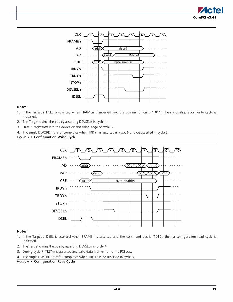
Configuration CyclesConfiguration read and write cycles are used to defineand determine the status of the Target’s internalconfiguration registers. Configuration cycles are the onlytype of transactions that use the IDSEL signal. Registerselection is defined by the contents of the address (bits 7down to 2). A configuration write is shown in Figure 5and a configuration read is shown in Figure 6 on page23. CorePCI will also support burst transactions toconfiguration space if required.
Memory / I/O Cycles
Zero-Wait-State Burst TransactionsZero-wait-state bursting enables transfer of a DWORD(32-bit PCI) or two DWORDs (64-bit PCI) for every clockcycle. All cycles are initiated with DP_START/DP_START64indicating a hit to the Target. The backend should thenlook at the BAR0_MEM_CYC and BAR1_CYC todetermine which space is being addressed. The RD_CYCand WR_CYC signals define the direction of the transfer.All of the *_CYC signals become valid during theDP_START pulse cycle and will remain in the this stateuntil the next DP_START occurs. If a DP_START64 iscoincident with a DP_START, then the transaction isexpected to be 64 bits wide.
For PCI writes, the backend indicates that it is preparedto receive data by setting the WR_BE_RDY signal high.Valid data to the backend is qualified by theWR_BE_NOW bus. For PCI reads, the backend indicatesthat it is prepared to provide read data by setting theRD_BE_RDY signal. The PCI controller will respond on afollowing cycle with a RD_BE_NOW signal, whichqualifies the read data. The data is then transferred tothe PCI bus on the following cycle. In either the read orwrite case, the core will automatically increment theaddress.
Figure 3 • Input Timing for PCI Signals
Figure 4 • Output Timing for PCI Signals
T_h
InputsValid
CLK
T_su
CLK
TristateOutput
T_val
T_off
T_on
OutputDelay
22 v4.0
CorePCI v5.41
Notes:
1. If the Target’s IDSEL is asserted when FRAMEn is asserted and the command bus is '1011', then a configuration write cycle isindicated.
2. The Target claims the bus by asserting DEVSELn in cycle 4.
3. Data is registered into the device on the rising edge of cycle 5.
4. The single DWORD transfer completes when TRDYn is asserted in cycle 5 and de-asserted in cycle 6.Figure 5 • Configuration Write Cycle
Notes:
1. If the Target’s IDSEL is asserted when FRAMEn is asserted and the command bus is '1010', then a configuration read cycle isindicated.
2. The Target claims the bus by asserting DEVSELn in cycle 4.
3. During cycle 7, TRDYn is asserted and valid data is driven onto the PCI bus.
4. The single DWORD transfer completes when TRDYn is de-asserted in cycle 8.Figure 6 • Configuration Read Cycle
1 2 3 4 5 6 7 8CLK
addr
IDSEL
1011
Paddr
data0
Pdata0
byte enables
FRAMEn
AD
CBE
IRDYn
TRDYn
DEVSELn
PAR
STOPn
CLK
IDSEL
FRAMEn
AD
CBE
IRDYn
TRDYn
DEVSELn
PAR
STOPn
1 2 3 4 5 6 7 8 9 10
data0
Pd0
byte enables1010
addr
Paddr
v4.0 23
CorePCI v5.41
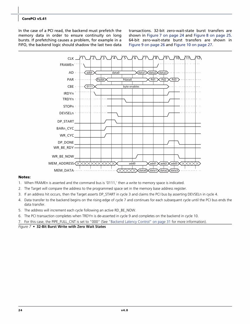
In the case of a PCI read, the backend must prefetch thememory data in order to ensure continuity on longbursts. If prefetching causes a problem, for example in aFIFO, the backend logic should shadow the last two data
transactions. 32-bit zero-wait-state burst transfers areshown in Figure 7 on page 24 and Figure 8 on page 25.64-bit zero-wait-state burst transfers are shown inFigure 9 on page 26 and Figure 10 on page 27.
Notes:
1. When FRAMEn is asserted and the command bus is '0111,' then a write to memory space is indicated.
2. The Target will compare the address to the programmed space set in the memory base address register.
3. If an address hit occurs, then the Target asserts DP_START in cycle 3 and claims the PCI bus by asserting DEVSELn in cycle 4.
4. Data transfer to the backend begins on the rising edge of cycle 7 and continues for each subsequent cycle until the PCI bus ends thedata transfer.
5. The address will increment each cycle following an active RD_BE_NOW.
6. The PCI transaction completes when TRDYn is de-asserted in cycle 9 and completes on the backend in cycle 10.
7. For this case, the PIPE_FULL_CNT is set to "000" (See "Backend Latency Control" on page 31 for more information).Figure 7 • 32-Bit Burst Write with Zero Wait States
CLK
addr
0111
Paddr
data0
Pdata0
data1 data2 data3
Pd1 Pd2 Pd3
byte enables
add1 add2 add3
data1 data2 data3data0
add0
1 2 3 4 5 6 7 8 9 10 11 12
FRAMEn
AD
CBE
IRDYn
TRDYn
DEVSELn
PAR
STOPn
MEM_ADDRESS
MEM_DATA
DP_DONE
BARn_CYC
WR_BE_RDY
WR_BE_NOW
WR_CYC
DP_START
24 v4.0
CorePCI v5.41
Notes:
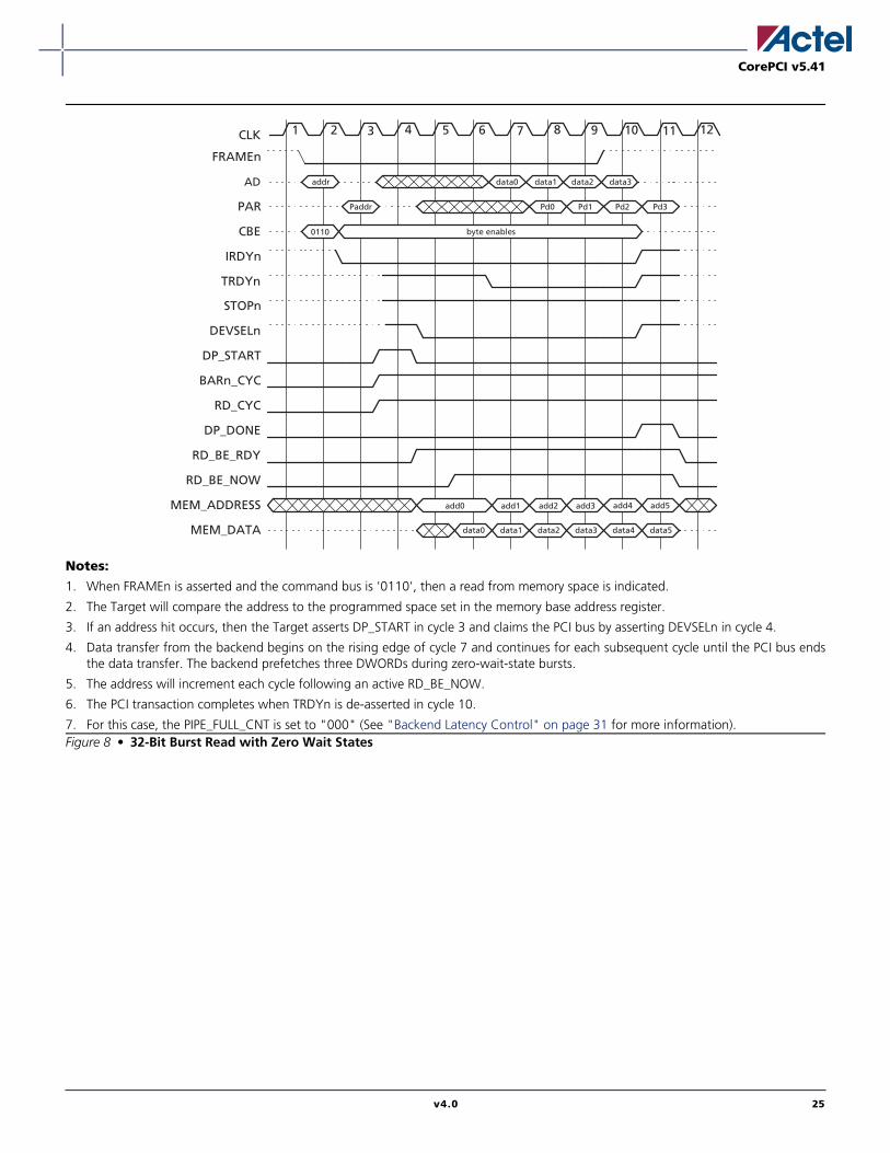
1. When FRAMEn is asserted and the command bus is '0110', then a read from memory space is indicated.
2. The Target will compare the address to the programmed space set in the memory base address register.
3. If an address hit occurs, then the Target asserts DP_START in cycle 3 and claims the PCI bus by asserting DEVSELn in cycle 4.
4. Data transfer from the backend begins on the rising edge of cycle 7 and continues for each subsequent cycle until the PCI bus endsthe data transfer. The backend prefetches three DWORDs during zero-wait-state bursts.
5. The address will increment each cycle following an active RD_BE_NOW.
6. The PCI transaction completes when TRDYn is de-asserted in cycle 10.
7. For this case, the PIPE_FULL_CNT is set to "000" (See "Backend Latency Control" on page 31 for more information).Figure 8 • 32-Bit Burst Read with Zero Wait States
CLK
addr
0110
Paddr
data1 data2 data3
Pd1 Pd2 Pd3
add2 add3 add4
data2 data3 data4data1
1 2 3 4 5 6 7 8 9 10 11 12
data0
Pd0
add1
data0
byte enables
FRAMEn
AD
CBE
IRDYn
TRDYn
DEVSELn
PAR
STOPn
MEM_ADDRESS
MEM_DATA
DP_DONE
DP_START
RD_BE_RDY
RD_BE_NOW
add0 add5
data5
BARn_CYC
RD_CYC
v4.0 25

CorePCI v5.41
Notes:
1. When FRAMEn and REQ64n is asserted and the command bus is '0111', then a 64-bit write to memory space is indicated.
2. The Target will compare the address to the programmed space set in the memory base address register.
3. If an address hit occurs, then the Target asserts DP_START and DP_START64 in cycle 3 and claims the PCI bus by asserting DEVSELnand ACK64n in cycle 4.
4. Data transfer to the backend begins on the rising edge of cycle 7 and continues for each subsequent cycle until the PCI bus ends thedata transfer.
5. For 64-bit transfer, the MEM_ADDRESS will increment by 2 for each cycle.
6. The PCI transaction completes when TRDYn is de-asserted in cycle 10.
7. For this case, the PIPE_FULL_CNT is set to '000' (See "Backend Latency Control" on page 31 for more information).
8. See "Backend Latency Control" on page 31 for RD_CYC and BARn_CYC timing.Figure 9 • 64-bit Burst Write with Zero Wait States
CLK
zero
0111
Paddr
data1
Pdata1
data3 data5 data7
Pd3 Pd5 Pd7
byte enables
add2 add4 add6
data3 data5 data7data1
add0
1 2 3 4 5 6 7 8 9 10 11 12
FRAMEn
AD[63:32]
CBE
IRDYn
TRDYn
DEVSELn
PAR
STOPn
MEM_ADDRESS
MEM_DATA[63:32]
DP_DONE
DP_START
WR_BE_RDY
WR_BE_NOW
REQ64n
zero Pdata0 Pd2 Pd4 Pd6PAR64
ACK64n
DP_START64
WR_BE_NOW64
1111
1111
0000
0000
0000
0000
addr data0 data2 data4 data6AD[31:0]
data2 data4 data6data0MEM_DATA[31:0]
26 v4.0
CorePCI v5.41
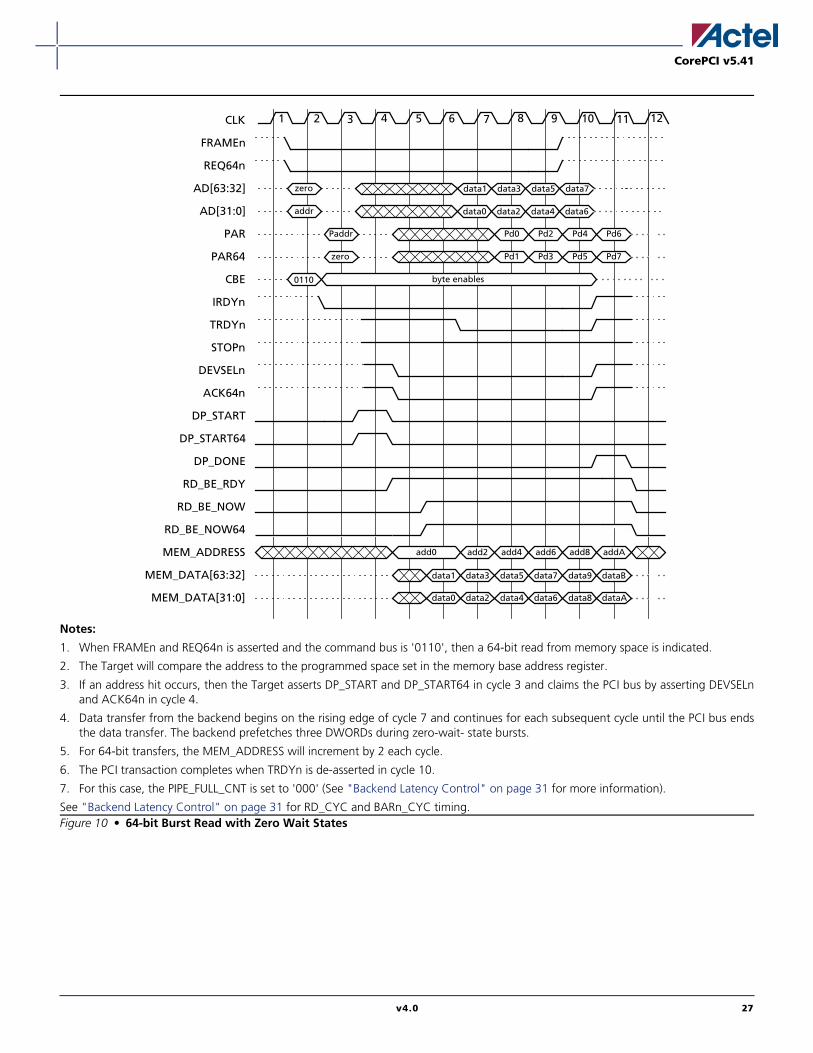
Notes:
1. When FRAMEn and REQ64n is asserted and the command bus is '0110', then a 64-bit read from memory space is indicated.
2. The Target will compare the address to the programmed space set in the memory base address register.
3. If an address hit occurs, then the Target asserts DP_START and DP_START64 in cycle 3 and claims the PCI bus by asserting DEVSELnand ACK64n in cycle 4.
4. Data transfer from the backend begins on the rising edge of cycle 7 and continues for each subsequent cycle until the PCI bus endsthe data transfer. The backend prefetches three DWORDs during zero-wait- state bursts.
5. For 64-bit transfers, the MEM_ADDRESS will increment by 2 each cycle.
6. The PCI transaction completes when TRDYn is de-asserted in cycle 10.
7. For this case, the PIPE_FULL_CNT is set to '000' (See "Backend Latency Control" on page 31 for more information).
See "Backend Latency Control" on page 31 for RD_CYC and BARn_CYC timing.Figure 10 • 64-bit Burst Read with Zero Wait States
CLK
zero
0110
Paddr
data3 data5 data7
Pd2 Pd4 Pd6
add4 add6 add8
data5 data7 data9data3
1 2 3 4 5 6 7 8 9 10 11 12
data1
Pd0
add2
data1
byte enables
FRAMEn
AD[63:32]
CBE
IRDYn
TRDYn
DEVSELn
PAR
STOPn
MEM_ADDRESS
MEM_DATA[63:32]
DP_DONE
DP_START
RD_BE_RDY
RD_BE_NOW
REQ64n
zero Pd3 Pd5 Pd7Pd1PAR64
addr data2 data4 data6data0AD[31:0]
ACK64n
DP_START64
RD_BE_NOW64
data4 data6 data8data2data0MEM_DATA[31:0]
add0 addA
dataB
dataA
v4.0 27

CorePCI v5.41
Paced TransactionsBackend throttle transfers provide a handshakemechanism for supporting slow response devices. Thebackend transactions are paced using the RD_BE_RDYand WR_BE_RDY signals. These signals can be used topace either single DWORD or burst transactions.
Figure 11 and Figure 12 on page 29 illustrate thismechanism for a backend that requires three cycles torespond to a read or write command from the PCIbus.
Notes:
1. The WR_BE_RDY can be asserted two cycles before the backend is ready to receive data.
2. The WR_BE_RDY signal is asserted on cycle 4 (cycle 7), causing the assertion of TRYDYn on cycle 5 (cycle 8), completing the PCI writecycle. One cycle later, the data is available on the backend and is qualified by the WR_BE_NOW[3:0] bus.
3. The WR_BE_NOW[3:0] should not be assumed to happen at this time (cycle 6 or cycle 9) because it is also dependent on the state ofIRDYn.
4. See Figure 7 on page 24 for WR_CYC and BARn_CYC timing.Figure 11 • Write Using Backend Throttling
CLK
addr
0111
Paddr
FRAMEn
AD[31:0]
CBE[3:0]
IRDYn
TRDYn
DEVSELn
PAR
STOPn
data0
Pdata0
MEM_ADDRESS[23:2]
MEM_DATA[31:0]
DP_DONE
DP_START
WR_BE_RDY
WR_BE_NOW
byte enables
data1data0
add0
1 2 3 4 5 6 7 8 9 10 11 12
Pd1
add1
data1
28 v4.0

CorePCI v5.41
Paused TransactionsDuring long bursts, either the backend controller or thePCI Master may insert wait states to accommodate somefunctional requirement. The PCI Master inserts waitstates by de-asserting the IRDYn signal. The wait state isindicated to the backend by de-assertion of theWR_BE_NOW bus or the RD_BE_NOW signal.
The backend can insert wait states by de-assertion of the*_BE_RDY signals. These signals cause the Target
controller to de-assert TRDYn and insert wait states onthe PCI bus. For writes, the backend must be prepared toaccept up to two DWORDs of data prior to data transfertermination. For reads, the backend must be prepared totransmit one DWORD of data prior to data transfertermination. Paused transactions are shown in Figure 13and Figure 14 on page 31.
Notes:
1. The RD_BE_RDY can be asserted one cycle before the backend is ready to transmit data.
2. The RD_BE_RDY signal is asserted on cycle 5 (cycle 8) and will initiate assertion of RD_BE_NOW latching the data into the controller.The data transfer will complete when TRDYn is asserted on the following cycle 7 (cycle 10).
3. The RD_BE_NOW should not be assumed to happen at this time (cycle 6 or 9) because it is also dependent on the state of IRDYn.
4. See Figure 8 on page 25 for RD_CYC and BARn_CYC timing.Figure 12 • Read Using Backend Throttling
CLK
addr
0110
Paddr
FRAMEn
AD[31:0]
CBE[3:0]
IRDYn
TRDYn
DEVSELn
PAR
STOPn
MEM_ADDRESS[23:2]
MEM_DATA[31:0]
DP_DONE
DP_START
RD_BE_RDY
RD_BE_NOW
data0
Pd0
data0
1 2 3 4 5 6 7 8 9 10 11 12
add0
data1
add1
data1
Pd0
1413
byte enables
add2
v4.0 29

CorePCI v5.41
Notes:
1. In the example, the flow of data is interrupted from the PCI Master de-assertion of IRDYn in cycle 3. The PCI Master inserts two waitstates. This state of the PCI bus is defined to the backend by de-asserting the WR_BE_NOW[3:0] bus one cycle later.
2. The backend can also interrupt the flow of data by de-asserting the WR_BE_RDY signal. One cycle later, TRDYn is de-asserted, haltingthe flow of data on the PCI bus. The backend must accept two DWORDs of data following de-assertion of the WR_BE_RDY signal.
Figure 13 • PCI Write Illustrating both IRDYn and TRDYn De-Assertion
CLK
FRAMEn
AD[31:0]
CBE[3:0]
IRDYn
TRDYn
DEVSELn
PAR
STOPn
MEM_ADDRESS[23:2]
MEM_DATA[31:0]
DP_DONE
DP_START
WR_BE_RDY
WR_BE_NOW
data2 data3
Pd2 Pd3
add1 add2
data1 data2
13 14 15 165 6 7 8 9 10 11 121 2 3 4
Pd1
data4
Pd4
data6 data7 data8 data11
Pd6 Pd7 Pd8 Pd9
add3
data3
add4
data4
data5
Pd5
data9
byte enables
data10 data12
Pd10 Pd11
data5
add5 add6 add7 add8 add9
data6 data7 data8 data9
add10 add11
data11data10
30 v4.0

CorePCI v5.41
Backend Latency ControlSome backends require the address to be available atleast one cycle prior to data being valid. This is true formost synchronous backends. In order to support thisneed, CorePCI provides the PIPE_FULL_CNT control bus tothe backend. This bus can be used to define the relativedelay between address and data. When thePIPE_FULL_CNT is set to '000', the address will beexpected to be coincident with the data and the datashould be valid whenever the *NOW lines are asserted.
When PIPE_FULL_CNT is set to a non-zero value, then theoperation of the backend is as follows:
• The backend asserts the *RDY signal.
• The *NOW signal will assert, and the address willbegin incrementing. However, the data is notexpected to be valid until N cycles after the valuedefined on the PIPE_FULL_CNT bus.
• Once the initial time-out occurs, valid data mustbe available whenever the *NOW signal isasserted.
Figure 15 is an example of this function for a read cyclewith the PIPE_FULL_CNT set to '001'.
Notes:
1. In the example, the PCI Master interrupts the flow of data by de-asserting the IRDYn sign in cycle 4. One cycle later, RD_BE_NOWsignal becomes inactive indicating that the backend should stop supplying data.
2. The backend can also interrupt the flow of data by de-asserting the RD_BE_RDY signal. The backend should be prepared to provideone additional DWORD of data to the PCI bus prior to halting the data flow. One cycle after RD_BE_RDY is de-asserted, theRD_BE_NOW signal is driven inactive, which is then followed by the de-assertion of TRDYn.
Figure 14 • PCI Read Illustrating both IRDYn and TRDYn De-Assertion
CLK
FRAMEn
AD[31:0]
CBE[3:0]
IRDYn
TRDYn
DEVSELn
PAR
STOPn
MEM_ADDRESS[23:2]
MEM_DATA[31:0]
DP_DONE
DP_START
RD_BE_RDY
RD_BE_NOW
data2 data3
Pd2 Pd3
add3 add4
data3 data4
13 14 15 165 6 7 8 9 10 11 121 2 3 4
Pd1
data4 data5
Pd4 Pd5
data6 data7 data8 data9 data10 data11
Pd6 Pd7 Pd8 Pd9 Pd10
add5
data5
add6
data6 data7
data12
Pd11
data8 data9
add7 add8 add9 add10
data10
add11 add12 add13
data11 data12 data13
byte enables
v4.0 31

CorePCI v5.41
Target AbortThe backend may cause a target abort (Figure 16) by asserting the ERROR input. The ERROR input will cause a Targetabort, which is defined by the Target simultaneously asserting the STOPn signal and de-asserting the DEVSELn signal.
Figure 15 • Backend Latency Read Transaction
CLK
addr
0110
Paddr
data1 data2
Pd1 Pd2
add2 add3 add4
data2 data3 data4data1
1 2 3 4 5 6 7 8 9 10 11 12
data0
Pd0
add1
data0
byte enables
FRAMEn
AD
CBE
IRDYn
TRDYn
DEVSELn
PAR
STOPn
MEM_ADDRESS
MEM_DATA
DP_DONE
DP_START
RD_BE_RDY
RD_BE_NOW
add0 add5
data5
PIPE_FULL_CNT 000 001
add6
Notes:1. During a PCI cycle, the backend ERROR signal indicates that a problem occurred on the backend such that the transfer cannot be
completed.2. The Target initiates a Target abort by asserting STOPn and de-asserting DEVSELn in the same cycle.3. The Master will begin cycle termination by de-asserting FRAMEn first, and then IRDYn on a subsequent cycle.4. The transaction completes when STOPn is de-asserted in cycle 9.5. The *_BE_RDY signal should be de-asserted whenever the ERROR signal is asserted.Figure 16 • Target Abort Cycle
CLK
addr
0111
Paddr
FRAMEn
AD[31:0]
CBE[3:0]
IRDYn
TRDYn
DEVSELn
PAR
STOPn
data0
Pdata0
ERROR
1 2 3 4 5 6 7 8 9 10 11 12
data3
Pd3
byte enables
data1
Pd1 Pd2
data2
32 v4.0

CorePCI v5.41
Target Retry and Disconnect When the backend is busy or unable to provide the datarequested, the Target controller will respond with eithera retry or a disconnect cycle. If the backend hasarbitrated for control of the backend bus and theBE_GNT signal is active, then the controller will respondwith a retry cycle (Figure 17). The Target indicates that itis unable to respond by asserting STOPn and DEVSELnsimultaneously.
During a regular PCI transfer, the RD_BE_RDY andWR_BE_RDY indicate that data is available to be receivedfrom or transmitted to the backend. If, during a PCIcycle, the backend becomes unable to read or write data,then the *_RD_RDY signals are de-asserted. After severalcycles, a PCI time-out will occur and the Target controllerwill initiate a Target disconnect without data cycle(Figure 18 on page 34).
Notes:1. If BE_GNT or BUSY are asserted at the beginning of a cycle, then a retry is initiated.2. The Target simultaneously asserts the STOPn and DEVSELn signals without asserting the TRDYn signal.3. The Master will begin cycle termination by de-asserting FRAMEn first and then IRDYn on a subsequent cycle.Figure 17 • Target Retry
CLK
addr
0110
Paddr
FRAMEn
AD[31:0]
CBE[3:0]
IRDYn
TRDYn
DEVSELn
PAR
STOPn
1 2 3 4 5 6 7 8
byte enables
BE_GNT
v4.0 33

CorePCI v5.41
Backend ArbitrationWhen the backend needs to take control of the backendbus, it should arbitrate for control using the BE_REQ andBE_GNT handshake signals (Figure 19 on page 34).
InterruptTo initiate an interrupt, the backend needs to assert theEXT_INTn input (Figure 20 on page 35). Two cycles laterthe PCI INTAn interrupt signal will assert.
Notes:
1. During a normal PCI transaction, the backend reaches a point where it is unable to deliver data and de-asserts RD_BE_RDY.
2. If the backend cannot deliver new data within 8 cycles, then it should assert the BUSY signal.
3. The Target initiates a disconnect by asserting the STOPn signal.
4. The Master will begin cycle termination by de-asserting FRAMEn first, and then IRDYn on a subsequent cycle.Figure 18 • Target Disconnect Without Data
CLK
FRAMEn
AD[31:0]
CBE[3:0]
IRDYn
TRDYn
DEVSELn
PAR
STOPn
MEM_ADDRESS[23:2]
MEM_DATA[31:0]
DP_DONE
DP_START
RD_BE_RDY
RD_BE_NOW
add5 add6 add7
data5 data6 data7
data4 data5 data6 data7
Pd4 Pd5 Pd6 Pd7Pd3
1 2 3 4 5 6 7 8 9 10 11 12
BUSY
Pd8
data8
add8
data8
add9
Notes:
1. Arbitration begins by the backend asserting the BE_REQ signal. The Target Controller will grant control as soon as the PCI controllergoes into an IDLE state.
2. The backend will maintain control as long as the BE_REQ signal remains active.
3. To relinquish control, the backend will de-assert the BE_REQ and BE_GNT will de-assert on the following cycle.Figure 19 • Backend Arbitration Cycle
CLK
BE_REQ
BE_GNT
34 v4.0

CorePCI v5.41
PCI Master TransactionsTo perform Master transfers for Master only,Target+DMA, and Target+Master functions, CorePCIcontroller has three configuration registers used to setaddresses, transfer length, control, and check status ofthe transfer. A basic sequence of events for executing aDMA or Master transfer is as follows:
1. Write the location of the desired PCI address intothe PCI Start Address register.
2. Write the location of the backend memorylocation into the RAM Start Address register.
3. Set the direction of the transfer using bit 3 of theDMA Control Register.
4. Define the transfer length using bits 27–16 in theDMA Control register. The length can be from asingle DWORD up to 1,024 DWORDs. The transferlength value should be all zeros for 1,024DWORDs.
5. Initiate the transfer by setting the DMA request,and enable bits 4 and 5 in the DMA Controlregister.
6. At completion, bit 1 in the DMA Control register isset to a '1'.
PCI DMA ReadDMA reads begin with arbitration for control of the PCIbus. The PCI request and grant signals are used toarbitrate Master access to the bus. Once control isgranted to the core, the core begins by assertingFRAMEn, the address on the AD bus, and the command'0110' on the CBE bus. A DMA read fetches data from thePCI bus and writes data to the backend memory. The coreasserts IRDYn and then waits for the addressed Target toprovide the data indicated by TRDYn assertion. Thetransfer continues until the DMA transfer length isreached. The waveforms shown in Figure 21 on page 36depict the action of the core when it operates as a DMAMaster in a zero-wait-state read transfer.
For DMA transactions, either zero-wait-state transfers orpaced transfers can be used. During DMA transactions,these two transfer modes function identically, as they doin a Target-only transaction.
Notes:
1. The EXT_INTn signal is sampled on the rising edge of eachclock.
2. If the EXT_INTn signal is asserted and sampled in cycle 2, thenthe PCI INTAn signal will be asserted in cycle 3.
Figure 20 • Interrupt
1 2 3 4CLK
EXT_INTn
INTAn
v4.0 35

CorePCI v5.41
PCI DMA WriteA DMA write begins by the core requesting control ofthe bus. Once the bus is granted (GNTn asserted), thecore will initiate the transfer by asserting FRAMEn. ADMA write reads information from RAM and writesinformation onto the PCI bus. The backend beginsfetching data and when data is available, the datapathpipe fills and data flows onto the PCI bus. At that point,IRDYn is asserted and the burst transfer begins. Thetransfer is terminated once the DMA transfer length is
reached. Figure 22 on page 37 shows the zero-wait-stateburst write transfer.
To control the Master-only core, four backend signals havebeen added. The new signals are CS_CONTROLn,RD_CONTROLn, WR_CONTROLn and CONTROL_ADD(1:0).Figure 25 and Figure 26 on page 39 show how thesesignals are used to read and write the DMA controlregisters, which in turn initiates PCI cycles.
Notes:
1. Once CorePCI is granted the PCI bus, the core asserts DP_START and begins the process of enabling the bus to drive FRAMEn.
2. The PCI address and command are valid at the same time that FRAMEn is driven low.
3. Once FRAMEn is driven, if the backend is prepared to supply data, then IRDYn is asserted on the following cycle. The core can storeup to two DWORDs of data. If the Target has not responded with a TRDYn when the second DWORD is read, then the core will ceasereading as indicated by the RD_BE_NOW signal de-asserting.
4. The core then waits for the Target to complete the transfer by asserting TRDYn.
5. The transfer continues until either the transfer count is exhausted or the Target disconnects.
6. Cycle termination is initiated by driving FRAMEn high.
7. The number of clock cycles from DP_START to FRAMEn assertion can be increased by asserting STALL_MASTER.Figure 21 • Zero-Wait-State Master DMA Read (Read from the PCI Bus)
CLK
FRAMEn
AD[31:0]
C_BE[3:0]
IRDYn
TRDYn
DEVSELn
PAR
STOPn
13 14 15 165 6 7 8 9 10 11 121 2 3 4
MEM_ADDRESS[23:2]
MEM_DATA[31:0]
WR_BE_NOW[3:0]
WR_BE_RDY
DP_START
data0 data1 data2 data3
data0 data1 data2 data3
addr1 addr2 addr3 addr4addr0
byte enables
Pd0 Pd1 Pd2 Pd3
addr
Paddr
CMD
DP_DONE
WR_CYC
BARn_CYC
36 v4.0
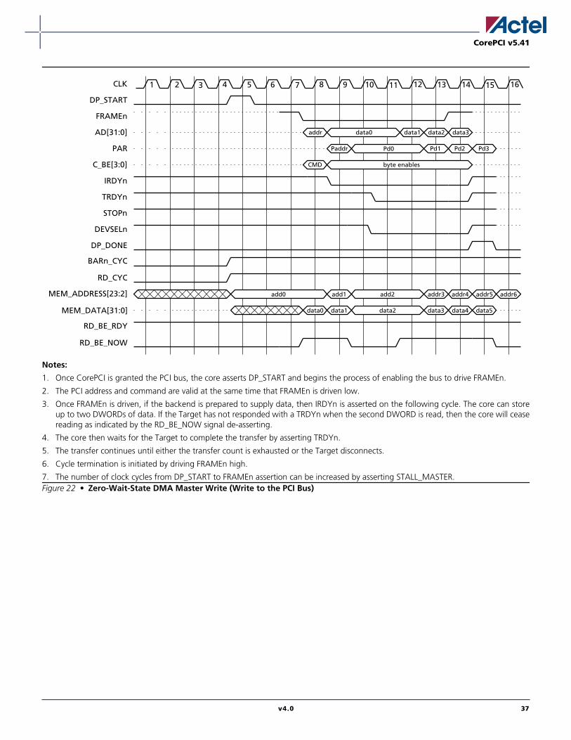
CorePCI v5.41
Notes:
1. Once CorePCI is granted the PCI bus, the core asserts DP_START and begins the process of enabling the bus to drive FRAMEn.
2. The PCI address and command are valid at the same time that FRAMEn is driven low.
3. Once FRAMEn is driven, if the backend is prepared to supply data, then IRDYn is asserted on the following cycle. The core can storeup to two DWORDs of data. If the Target has not responded with a TRDYn when the second DWORD is read, then the core will ceasereading as indicated by the RD_BE_NOW signal de-asserting.
4. The core then waits for the Target to complete the transfer by asserting TRDYn.
5. The transfer continues until either the transfer count is exhausted or the Target disconnects.
6. Cycle termination is initiated by driving FRAMEn high.
7. The number of clock cycles from DP_START to FRAMEn assertion can be increased by asserting STALL_MASTER.Figure 22 • Zero-Wait-State DMA Master Write (Write to the PCI Bus)
CLK
FRAMEn
AD[31:0]
C_BE[3:0]
IRDYn
TRDYn
DEVSELn
PAR
STOPn
13 14 15 165 6 7 8 9 10 11 121 2 3 4
MEM_ADDRESS[23:2]
MEM_DATA[31:0]
RD_BE_NOW
RD_BE_RDY
DP_START
data3 data4 data5
data1 data2 data3
addr3 addr4 addr5 addr6
byte enables
Pd1 Pd2 Pd3
addr
Paddr
CMD
data0
add0 add1 add2
data0 data1 data2
Pd0
DP_DONE
RD_CYC
BARn_CYC
v4.0 37

CorePCI v5.41
Backend Control of DMA ActivityThe core provides two signals, BUSY_MASTER andSTALL_MASTER, that can be used to control the DMAtransfers. BUSY_MASTER allows a DMA transfer to bestopped, and STALL_MASTER allows for slow backends tomeet the FRAME-to-IRDY assertion requirement for PCI.
If the backend asserts BUSY_MASTER when a DMAtransfer is taking place, the core will stop the DMA
transfer as soon as possible, as shown in Figure 22a. Dueto PCI protocol requirements the core may need totransfer an additional two words after BUSY_MASTERhas been asserted. The core will not restart the DMAtransfer until BUSY_MASTER has been de-asserted. Thebackend may assert BE_REQ at the same time, and whenBE_GNT is asserted may access the DMA control registers.The backend can then clear the DMA request bit in thecontrol register to cancel the rest of the DMA transfer.
When a DMA backend read cycle is started the core willstart a backend read cycle by asserting DP_START andtwo cycles later assert FRAME. Once FRAME is assertedthe PCI specification requires that the core assert IRDYwithin 8 clock cycles. The core cannot assert IRDY untilthe backend has asserted RD_BE_RDY. If the backend
asserts RD_BE_RDY after 7 clock cycles, the core willviolate the PCI FRAME to IRDY assertion timing. In thissituation the backend should assert STALL_MASTER untilit can assert RD_BE_RDY, this will delay the core-assertingFRAME until data is ready, causing the FRAME to IRDYdelay to be less than 8 clock cycles.
Figure 23 • DMA Master with BUSY_MASTER Asserted
STALL_MASTER
BUSY_MASTER
FRAMEn
AD[31:0]
CBE[3:0]
IRDYN
TRDYn
STOPn
DEVSELn
DP_DONE
RD_CYC
MEM_ADDRESS[23:2]
MEM_DATA[31:0]
RD_BE_RDY
RD_BE_NOW
addr data0 data1 data2 data3
CMD byte enables CMD
addr0 addr1 addr2 addr3 addr4 addr4
data0 data1 data2 data3 data4 data4
38 v4.0

CorePCI v5.41
When STALL_MASTER is active (see Figure 24), the core does not immediately assert FRAME and the PCI bus is idle. It ispossible for the PCI GNT to go away; in this case the core will stop the PCI transfer and assert DP_END.
Accessing the DMA Registers from the BackendA write to the DMA register is accomplished by assertingCS_CONTROLn, WR_CONTROLn, valid address, and validdata at the same time. Registers can be updated one at atime or in bursts by changing the address and data whilekeeping CS_CONTROLn and WR_CONTROLn asserted(Figure 25).
Reads from the DMA are pipelined with two cycles ofdelay between valid address and valid data. To enablethe output drivers, both CS_CONTROLn andRD_CONTROLn must be driven low (Figure 26).
Figure 24 • DMA Master with STALL_MASTER Asserted
CLK
DP_START
STALL_MASTER
BUSY_MASTER
FRAMEn
AD[31:0]
CBE[3:0]
IRDYN
TRDYn
STOPn
DEVSELn
DP_DONE
RD_CYC
MEM_ADDRESS[23:2]
MEM_DATA[31:0]
RD_BE_RDY
RD_BE_NOW
addr data0 data1 data2
CMD byte enables
addr0 addr1 addr2 addr3
data0 data1 data2
Figure 25 • Backend Write to a DMA Register
Figure 26 • Backend Read from a DMA Register
CLK
WE_CONTROLn
CS_CONTROLn
CONTROL_ADD[1:0] valid
MEM_DATA[31:0] valid
1 2 3 4
CLK
CS_CONTROLn
WE_CONTROLn
CONTROL_ADD[1:0]
MEM_DATA[31:0]
valid
valid
1 2 3 4 5 6 7 8 9 10
v4.0 39

CorePCI v5.41
Ordering InformationCorePCI v5.41 can be ordered through your local Actel sales representative. It should be ordered using the followingnumbering scheme; CorePCI-XX where XX corresponds to one of the variables in Table .
Table 23 • Ordering Codes
XX Description
EV Evaluation Version
SN Netlist for single-use on Actel devices
AN Netlist for unlimited use on Actel devices
SR RTL for single-use on Actel devices
AR RTL for unlimited use on Actel devices
UR RTL for unlimited use and not restricted to Actel devices
40 v4.0
CorePCI v5.41
List of ChangesThe following table lists critical changes that were made in the current version of the document.
Datasheet CategoriesIn order to provide the latest information to designers, some datasheets are published before data has been fullycharacterized. Datasheets are designated as "Product Brief," "Advanced," and "Production." The definitions of thesecategories are as follows:
Product BriefThe product brief is a summarized version of an advanced or production datasheet containing general productinformation. This brief summarizes specific device and family information for unreleased products.
AdvancedThis datasheet version contains initial estimated information based on simulation, other products, devices, or speedgrades. This information can be used as estimates, but not for production.
Unmarked (production)This datasheet version contains information that is considered to be final.
Previous Version Changes in Current Version (v4.0) Page
v4.0 ProASIC3/E data was added. –
v4.0 41

5172168-2/10.04
http://www.actel.com
Actel and the Actel logo are registered trademarks of Actel Corporation.All other trademarks are the property of their owners.
Actel Corporation
2061 Stierlin CourtMountain View, CA94043-4655 USAPhone 650.318.4200Fax 650.318.4600
Actel Europe Ltd.
Dunlop House, Riverside WayCamberley, Surrey GU15 3YLUnited KingdomPhone +44 (0) 1276 401 450Fax +44 (0) 1276 401 490
Actel Japan
EXOS Ebisu Bldg. 4F1-24-14 Ebisu Shibuya-kuTokyo 150 JapanPhone +81.03.3445.7671Fax +81.03.3445.7668
Actel Hong Kong
39th Floor, One Pacific Place88 Queensway, AdmiraltyHong Kong Phone +852.227.35712Fax +852.227.35999