Copyright by Mohammadreza Pourakbar 2017vuir.vu.edu.au/32299/1/POURAKBAR Mohammadreza -...
194
Transcript of Copyright by Mohammadreza Pourakbar 2017vuir.vu.edu.au/32299/1/POURAKBAR Mohammadreza -...
A TUNABLE LOW-ISOLATION DEVICE FOR ADAPTIVE
DUPLEXERS
College of Engineering and Science
Victoria University
Submitted in fulllment of the requirements for the degree of
Doctor of Philosophy
Mohammadreza Pourakbar
B.Eng. (Electronics), M.Eng. (Electronics)
November 2016
© Copyright by Mohammadreza Pourakbar 2017
All Rights Reserved
i

To my loving parents
and
my dearest love, Sara
ii

Doctor of Philosophy Declaration
I, Mohammadreza Pourakbar, declare that the Ph.D thesis entitled "A TUNABLE
LOW-ISOLATION DEVICE FOR ADAPTIVE DUPLEXERS" is no more than 100,000
words in length including quotes and exclusive of tables, gures, appendices, bibli-
ography, references and footnotes. This thesis contains no material that has been
submitted previously, in whole or in part, for the award of any other academic degree
or diploma. Except where otherwise indicated, this thesis is my own work.
Mohammadreza Pourakbar
Date: November 09, 2016
iii

Abstract
Today's fourth generation (4G) long term evolution (LTE) handsets using frequency
division duplex operate on two frequencies to provide simultaneous transmission and
reception. A duplexer isolates the sensitive receiver (Rx) circuits from the high-power
transmitter (Tx) output. The classical duplexer relies on two highly selective lters
using surface acoustic wave or thin lm bulk acoustic resonator technology. One is
placed in the transmitter path to attenuate the Tx noise in the Rx band and another
is placed in the receiver path to prevent the large Tx leakage signal from overloading
the receiver. These lters have low insertion loss and high linearity, but support only
one frequency band, are bulky and cannot be integrated into the receiver microcircuit.
A set of duplexers connected to the antenna through an antenna switch is therefore
required for multi-band operation, handicapping the radio handset in terms of cost
and size. The lack of a tunable duplexer alternative is a major drawback. The current
research trend is to make the duplexer frequency agile, adaptive and integrable.
In this thesis, single-band and multi-band integrated solutions of a low-isolation
device (LID) are proposed to provide the initial isolation for an adaptive duplexer
scheme employing cancelling loops. Firstly, two inductor-capacitor (LC) based single-
band tunable duplex lters are designed. The lters cover long-term evolution band
1 in steps using digitally switched capacitor banks with stacked eld-eect transistors
for voltage handling. Bandpass-bandstop structures are used, and the insertion loss
versus isolation trade-o is derived as a function of component quality factor (Q) and
impedance level. A fully integrated 0.25-µm Silicon-on-Sapphire solution provides
iv
isolation of 19 dB for the Tx leakage signal and 14 dB for the Tx noise that falls
into the receive band. Using o-chip passives on a printed circuit board improves the
above isolations to greater than 25 dB, primarily due to increased inductor quality
factor (Q). Insertion losses are comparable to hybrid balancing schemes but are still
above those of traditional solutions.
Secondly, two multi-band partially-integrated LIDs are evaluated. The rst proto-
type is a quad-band tunable LID, providing the required tuning range for LTE Bands
1,2,3, and 7. The circuit is implemented in a 0.13-µm Silicon-on-Insulator process
with o chip printed circuit inductors. Post layout simulations show isolations ex-
ceeding 30 dB at both transmit and receive frequencies for each specied LTE band.
The insertion loss from the power amplier output port to antenna port is below 2
dB in LTE band 1. The fabricated circuit occupies an area of 2.0mm× 1.2mm. The
second prototype using the older 0.25-µm silicon on sapphire process is limited to
LTE bands 1,2, and 3. The simulated isolation is well above 20 dB for LTE band 1
and almost 20 dB for the other two bands. Diculties in ip-chipping the connections
meant that testing could not be completed in the available time.
v

Acknowledgements
First of all, I would like to thank Allah for spreading my life with the beauty of
knowledge and lighting my heart with the amity of his fourteen Infallible and granting
the ability of eort to full my thesis.
Implementation of this thesis indebted to guidance, assistance, consultation and
support of great persons which without them would be many problems through this
journey.
My special thanks and gratitude goes to my supervisor prof. Michael Faulkner.
His endless kindness, patience and support not only made possible the completion of
this thesis but also help to develop my research skills.
I would like to express my appreciation to Prof. Henrik Sjöland, Associate.Prof.
Markus Törmänen, the sta of the RF ASIC group at Ericsson and Lund University,
Sweden, and Mr. Dan Nobbe, Peregrine Semiconductor, for their helpful assistance
and advice. I would also like to acknowledge Peregrine Semiconductor for silicon
donation and chip fabrication.
I would like to thank the sta of Graduate Research Centre (GRC) and College of
Engineering and Science. I want to acknowledge Mrs.Elizabeth Smith for her invalu-
able support and advice during past years. I must also thank Prof. Helen Borland,
Prof. Chris Perera, Prof. Stephen Bigger, Prof. Stephen Collins, Prof. Aladin Za-
yegh, Dr. Lesley Birch, Mrs. Sue Davis, Dr. Lance Linton, and Mrs. Shukonya Benka
for their kindness and encouragement. I would like to recognise Victoria University
for providing me the opportunity to undertake postgraduate studies in Australia.
vi

Many thanks to my colleagues, who have shared friendship, great moments and
memories with me.
I dedicate my thesis to my dear parents and beloved wife who, despite being
thousands of miles away always supported me and encouraged me with unconditional
love through this journey. To my dearest sister to whom I will always owe a debt of
gratitude for being there for my parents while my pursuit of education had taken me
away from them.
vii

Contents
Doctor of Philosophy Declaration iii
Abstract iv
Acknowledgements vi
List of Figures xii
List of Tables xx
Abbreviations xxii
Symbols xxix
1 Introduction 1
1.1 Background . . . . . . . . . . . . . . . . . . . . . . . . . . . . . . . . 1
1.2 Carrier Aggregation Concept . . . . . . . . . . . . . . . . . . . . . . . 2
1.3 Software Dened Radio . . . . . . . . . . . . . . . . . . . . . . . . . . 4
1.4 Duplexing . . . . . . . . . . . . . . . . . . . . . . . . . . . . . . . . . 4
1.5 Adaptive Duplexers . . . . . . . . . . . . . . . . . . . . . . . . . . . . 7
1.6 Implementation in Silicon . . . . . . . . . . . . . . . . . . . . . . . . 7
1.7 Research Goals . . . . . . . . . . . . . . . . . . . . . . . . . . . . . . 8
1.8 Research Contributions . . . . . . . . . . . . . . . . . . . . . . . . . . 10
1.9 Contents and Organisation of the Thesis . . . . . . . . . . . . . . . . 11
viii

2 Background Information 13
2.1 Cellular Systems . . . . . . . . . . . . . . . . . . . . . . . . . . . . . 13
2.2 LTE Frequency Bands and Arrangements . . . . . . . . . . . . . . . . 16
2.3 4G LTE Transceiver Architecture . . . . . . . . . . . . . . . . . . . . 19
2.3.1 Impact of Tx Leakage on the Receiver . . . . . . . . . . . . . 21
2.4 LTE UE Transceiver Design Requirements . . . . . . . . . . . . . . . 24
2.4.1 RF Transmitter Requirements . . . . . . . . . . . . . . . . . . 24
2.4.1.1 Intended Transmission Requirements . . . . . . . . . 24
2.4.1.2 Unwanted Emission Requirements . . . . . . . . . . 25
2.4.2 RF Receiver Requirements . . . . . . . . . . . . . . . . . . . . 28
2.4.2.1 Sensitivity Level and Dynamic Range . . . . . . . . . 28
2.4.2.2 Receiver Susceptibility to Interfering Signals . . . . . 29
2.5 Typical Duplexer Requirements for LTE . . . . . . . . . . . . . . . . 30
2.6 Summary . . . . . . . . . . . . . . . . . . . . . . . . . . . . . . . . . 32
3 Duplexing Techniques: Literature Survey 33
3.1 Theory of The Duplexer . . . . . . . . . . . . . . . . . . . . . . . . . 34
3.2 Passive Duplexing Methods . . . . . . . . . . . . . . . . . . . . . . . 36
3.2.1 SAW and FBAR Technology . . . . . . . . . . . . . . . . . . . 36
3.2.2 Dual Antenna Scheme . . . . . . . . . . . . . . . . . . . . . . 41
3.2.3 Microstrip Directional Couplers . . . . . . . . . . . . . . . . . 42
3.2.4 Spatial Duplexing . . . . . . . . . . . . . . . . . . . . . . . . . 44
3.2.5 CMOS and Lumped Component Solutions . . . . . . . . . . . 45
3.3 Adaptive Duplexing Methods . . . . . . . . . . . . . . . . . . . . . . 48
3.3.1 Reducing Isolation Requirements . . . . . . . . . . . . . . . . 48
3.3.2 Cancelling Loops . . . . . . . . . . . . . . . . . . . . . . . . . 48
3.4 Summary . . . . . . . . . . . . . . . . . . . . . . . . . . . . . . . . . 53
4 Tunable Duplex Filter Design: Theory 54
4.1 RLC Resonance Theory . . . . . . . . . . . . . . . . . . . . . . . . . 55
ix

4.2 Design of the Tunable Duplex Filter . . . . . . . . . . . . . . . . . . . 56
4.2.1 Low-Frequency Network (LFN) Filter . . . . . . . . . . . . . . 57
4.2.1.1 Tuning . . . . . . . . . . . . . . . . . . . . . . . . . . 59
4.2.1.2 Losses . . . . . . . . . . . . . . . . . . . . . . . . . . 60
4.2.2 High-Frequency Network (HFN) Filter . . . . . . . . . . . . . 64
4.2.2.1 Tuning . . . . . . . . . . . . . . . . . . . . . . . . . . 65
4.2.2.2 Losses . . . . . . . . . . . . . . . . . . . . . . . . . . 66
4.2.3 Duplexing Concept . . . . . . . . . . . . . . . . . . . . . . . . 67
4.3 Summary . . . . . . . . . . . . . . . . . . . . . . . . . . . . . . . . . 73
5 Silicon-on-Insulator Technologies 75
5.1 SOI Fabrication Process: Background . . . . . . . . . . . . . . . . . . 76
5.1.1 The SIMOX Method . . . . . . . . . . . . . . . . . . . . . . . 78
5.1.2 The BESOI Method . . . . . . . . . . . . . . . . . . . . . . . 78
5.1.2.1 The Smart-Cut Method . . . . . . . . . . . . . . . . 79
5.2 Bulk CMOS vs. SOI and SOS . . . . . . . . . . . . . . . . . . . . . . 80
5.3 Peregrine SOS Process Features . . . . . . . . . . . . . . . . . . . . . 81
5.4 STMicroelectonics SOI Process Features . . . . . . . . . . . . . . . . 83
5.5 SOI/SOS FET Switch Performance . . . . . . . . . . . . . . . . . . . 84
5.5.1 Biasing Considerations . . . . . . . . . . . . . . . . . . . . . . 87
5.5.2 Stacking FET's Approach . . . . . . . . . . . . . . . . . . . . 89
5.6 Summary . . . . . . . . . . . . . . . . . . . . . . . . . . . . . . . . . 93
6 Single-Band Tunable Duplex Filter: Implementation 94
6.1 SOS Duplex Filters: Overview . . . . . . . . . . . . . . . . . . . . . . 95
6.1.1 Digitally Switched Capacitor Bank (DSCB) . . . . . . . . . . 96
6.1.2 Pad-based ESD Protection Circuitry . . . . . . . . . . . . . . 100
6.1.3 Simulation Results . . . . . . . . . . . . . . . . . . . . . . . . 101
6.1.4 Measurement Results . . . . . . . . . . . . . . . . . . . . . . . 104
6.1.4.1 ESD Protection . . . . . . . . . . . . . . . . . . . . . 104
x

6.1.4.2 Tunable Duplex Filter . . . . . . . . . . . . . . . . . 106
6.2 PCB Duplex Filters: Proof of Concept . . . . . . . . . . . . . . . . . 112
6.3 Summary . . . . . . . . . . . . . . . . . . . . . . . . . . . . . . . . . 118
7 Multi-band Tunable Duplex Filters: Simulation 119
7.1 Die-to-Substrate Interconnects for High-Q PCB Inductors . . . . . . . 120
7.1.1 Chip-to-Substrate Interconnections . . . . . . . . . . . . . . . 120
7.1.1.1 Wire-bond Connection Model . . . . . . . . . . . . . 120
7.1.1.2 Flip-chip Connection Model . . . . . . . . . . . . . . 121
7.1.2 Planar Laminate Inductor Design . . . . . . . . . . . . . . . . 124
7.1.2.1 Theoretical Consideration . . . . . . . . . . . . . . . 124
7.1.2.2 Practical Consideration . . . . . . . . . . . . . . . . 127
7.1.3 Simulation Results . . . . . . . . . . . . . . . . . . . . . . . . 129
7.2 Quad-band SOI Duplex Filter . . . . . . . . . . . . . . . . . . . . . . 130
7.2.1 SOI DSCB Design . . . . . . . . . . . . . . . . . . . . . . . . 132
7.2.2 High-Q Laminated Inductor Design . . . . . . . . . . . . . . . 135
7.2.3 Simulation Results . . . . . . . . . . . . . . . . . . . . . . . . 136
7.3 Triple-band SOS Duplex Filter . . . . . . . . . . . . . . . . . . . . . . 139
7.3.1 Simulation Results . . . . . . . . . . . . . . . . . . . . . . . . 141
7.4 Summary . . . . . . . . . . . . . . . . . . . . . . . . . . . . . . . . . 143
8 Conclusion 144
8.1 Future Work . . . . . . . . . . . . . . . . . . . . . . . . . . . . . . . . 149
References 151
xi

List of Figures
1.1 Data rate evolution in downlink with the CA. . . . . . . . . . . . . . 2
1.2 LTE-A carrier aggregation scenarios; Intra-band and inter-band aggre-
gation alternatives.(eNodeB means "evolved NodeB". The LTE bases-
tation that has evolved from the previous (third) generation UMTS.) 3
1.3 Duplexing modes used in modern mobile communication systems. . . 5
1.4 Multi-band RF front-end solution: (a) using number of switched du-
plexers (b) using an adaptive duplexer with a low-isolation device (LID)
and an active cancellation unit. . . . . . . . . . . . . . . . . . . . . . 6
1.5 Multi-band RF front-end solution: (a) using number of switched du-
plexers (b) using an adaptive duplexer with a low-isolation device (LID)
and an active cancellation unit. . . . . . . . . . . . . . . . . . . . . . 8
1.6 Spectrum of the transmitter output (red), the receiver input (green)
and the frequency response of the cancelling loops (black) required to
cancel both the strong Tx signal and Tx noise in the vicinity of the
received signal. . . . . . . . . . . . . . . . . . . . . . . . . . . . . . . 9
2.1 History of cellular communication standards. . . . . . . . . . . . . . . 14
2.2 LTE-FDD frequency band fragmentation showing uplink (red) and
downlink (green) frequencies. . . . . . . . . . . . . . . . . . . . . . . 16
2.3 LTE-FDD frequency band denitions. . . . . . . . . . . . . . . . . . . 17
2.4 A simplied typical transceiver architecture of a 4G cellular phone. . 19
2.5 Conventional duplexer consists of two front-end BPFs. . . . . . . . . 20
xii
2.6 Transmitter noise in the Rx band is attenuated by BPFTx. . . . . . . 20
2.7 Receiver desensitisation due to overload by the Tx signal unless atten-
uated by BPFRx. . . . . . . . . . . . . . . . . . . . . . . . . . . . . . 21
2.8 Cross-modulation distortion eect due to the strong Tx leakage. . . . 21
2.9 Second-order nonlinearity eect due to the strong Tx leakage. . . . . 22
2.10 Reciprocal mixing eect. . . . . . . . . . . . . . . . . . . . . . . . . . 23
2.11 LTE transmitter spectrum [8]. (RBs: Resource Blocks). . . . . . . . 25
2.12 SEM for a UE transmitter for various LTE channel bandwidths [8]. . 26
2.13 Illustration of ACLR for two nearby radio channels. . . . . . . . . . . 27
2.14 Tx leakage problem in LTE-FDD UE transceiver [8]. . . . . . . . . . . 31
3.1 Typical frequency response of the duplexer. . . . . . . . . . . . . . . . 35
3.2 Design trade-os for duplexers. . . . . . . . . . . . . . . . . . . . . . 36
3.3 Cross section of (a) stacked SAW lter on a transceiver [11] (b) FBAR
lter integrated above IC [12] (c) BAW resonator with solder bumps [13]. 37
3.4 UMTS-1 duplexer topology [14]. . . . . . . . . . . . . . . . . . . . . . 38
3.5 Schematic of tunable duplexer [16]. . . . . . . . . . . . . . . . . . . . 39
3.6 Size reduction of passive duplexers for handsets. . . . . . . . . . . . . 40
3.7 Decoupling technique for two antennas (a) function blocks (b) two
closely spaced miniaturised monopole antennas [20]. . . . . . . . . . . 41
3.8 Block diagram of self-cancelling technique for full-duplex RF commu-
nication systems [21]. . . . . . . . . . . . . . . . . . . . . . . . . . . . 42
3.9 Proposed reected power canceller employing the coupled-line direc-
tional coupler (a) operating principle (b) measured Tx-to-Rx isolation
and Tx reection [26]. . . . . . . . . . . . . . . . . . . . . . . . . . . 43
3.10 Evolution of spatial duplexing concept. (a) conventional duplexing.
(b) Tx-Rx separation mode by dual antenna. (c) a spatial duplexing
lter (d) notations [28]. . . . . . . . . . . . . . . . . . . . . . . . . . . 44
3.11 Tx/Rx module schematic [31]. . . . . . . . . . . . . . . . . . . . . . . 45
xiii
3.12 Dierential lter with equal value bond wires as inductor replace-
ments [35]. . . . . . . . . . . . . . . . . . . . . . . . . . . . . . . . . . 46
3.13 Integrated electrical balance duplexers using (a) hybrid autotransformer [38]
(b) hybrid transformer [39] (c) dierential transformers [40]. . . . . . 47
3.14 LMS adaptive lter architecture proposed by [46]. . . . . . . . . . . . 49
3.15 An auxiliary up-conversion chain for active cancellation concept [49]. 50
3.16 Block diagram for the adaptive duplexer (a) single-path feed-forward
operation. (b) dual-path feed-forward operation [51]. . . . . . . . . . 51
3.17 Adaptive duplexer (a) a dual-path feed-forward architecture. (b) the
spectrum of the received signal [52]. . . . . . . . . . . . . . . . . . . . 52
4.1 Q-factor of an RLC resonator (fres=2GHz, R=1Ω, G=0.01S, L=1nH,
C=6.33pF). . . . . . . . . . . . . . . . . . . . . . . . . . . . . . . . . 56
4.2 Coil-saving lter topologies:(a) LFN (b) HFN. . . . . . . . . . . . . . 57
4.3 Magnitude of Zeq vs frequency for 2% increments in the nominal value
of C1 (from the right). (Q = 100) . . . . . . . . . . . . . . . . . . . . 58
4.4 LFN frequency sensitivity to C1 and C2 (targeting LTE1 with L1 =
8.4nH, C1 = 0.77pF , and C2 = 3.82pF ): (a) ftx and frx (b) fd. . . . . 60
4.5 LFN equivalent circuit resonating at: (a) ftx (b) frx. . . . . . . . . . 61
4.6 LFN design trade-os (a) ILTX for dierent QL1 and QC1 (contours
in dB) (b) ISORX for dierent QL1, QC1 with QC2=10 (Solid) and
QC2=120 (Dotted). ILTX (Dotted blue) and ISORX (Solid red) plots
versus normalised impedance level for dierent Q's (increments of 25)
(c) ∆ = 10% (190 MHz) (d) ∆ = 5% (95MHz). . . . . . . . . . . . . . 63
4.7 HFN frequency sensitivity to C4 and C5 (targeting LTE1): (a) ftx and
frx (b) fd. . . . . . . . . . . . . . . . . . . . . . . . . . . . . . . . . . 65
4.8 HFN equivalent circuit resonating at: (a) frx (b) ftx. . . . . . . . . . 66
xiv
4.9 HFN ILRX (Solid red) and ISOTX (Dotted blue) plots versus nor-
malised impedance level and dierent Q's (increments of 25): (a)
∆ = 10% (b) ∆ = 5%. . . . . . . . . . . . . . . . . . . . . . . . . . . 67
4.10 Proposed tunable duplex lter conguration. . . . . . . . . . . . . . . 68
4.11 Normalised peak voltage ( VC√RL
) contours across C1 and C4 at ftx versus
TX power and normalised impedance. (note: The component Q's are
pinned to innity.) . . . . . . . . . . . . . . . . . . . . . . . . . . . . 69
4.12 Proposed coil-saving (dual) LFN lter topology. . . . . . . . . . . . . 70
4.13 The LFN lter performance- TOP: Tuning of C7 and C8: (a) ftx and
frx (b) fd. BOT: ILTX (Solid red) and ISORX (Dotted blue) plots
versus normalised impedance level for dierent Q's (increments of 20)
(c) ∆ = 10% (d) ∆ = 5%. . . . . . . . . . . . . . . . . . . . . . . . . 71
4.14 Peak Current through L3 (Solid blue) and C8 (Dotted red) normalised
to the load current versus ∆ for Fig. 4.12. . . . . . . . . . . . . . . . 72
4.15 Proposed tunable duplex lter conguration modied for the LFN lter. 73
5.1 SOI wafer manufacturing from SMART-CutTM UNIBOND TM wafer
bonding process. . . . . . . . . . . . . . . . . . . . . . . . . . . . . . 79
5.2 Cross-section of an inverter circuit in (a) bulk CMOS (b) SOI (c) SOS
process [66]. . . . . . . . . . . . . . . . . . . . . . . . . . . . . . . . . 80
5.3 Circuit model of (a) switch (SW) FET (b) FET equivalent model in
the ON-state (c) FET equivalent model in the OFF-state. . . . . . . 84
5.4 A switch FET test circuit: SOI process (left) and SOS process (right). 85
5.5 The on-resistance of a 58 nger device as a function of the gate voltage
(VBias) and FET periphery (nger width). . . . . . . . . . . . . . . . 86
5.6 Stacking FET's approch. . . . . . . . . . . . . . . . . . . . . . . . . . 89
xv

5.7 Voltage distribution for eight stacked SOS FET's switches when the
input power hits 39.5dBm. (a) Voltage waveforms at dierent drain
nodes (VD) of transistors M1-M8, (b) Drain-to-source Voltages (VDS1 ∼VDS8). (c) Gate-to-source voltages (VGS1 ∼ VGS8). (d) Gate-to-drain
voltage waveforms (VGD1 ∼ VGD8). Simulations in ADS (Advanced
Design System) using TIN device models. . . . . . . . . . . . . . . . . 91
5.8 Linearity and compression behaviour of the SOS stacked FET's switch. 92
5.9 Linearity and intermodulation behaviour of the SOS stacked FET's
switch. . . . . . . . . . . . . . . . . . . . . . . . . . . . . . . . . . . . 92
6.1 Adaptive duplexer architecture. (The wideband circulator is replaced
by L-C duplexing lters.) . . . . . . . . . . . . . . . . . . . . . . . . . 95
6.2 Single-band tunable SOS duplex lter. . . . . . . . . . . . . . . . . . 96
6.3 3-bits DSCB (a) simplied model (b) model in ON and OFF conditions. 97
6.4 3-bit DSCB: (a) 7 FET stack (b) capacitance control range and Q. . . 99
6.5 Pad-based ESD protection circuitry: the path of ESD current pulse
during a (a) positive (b) negative ESD event, (c) ESD layout. . . . . 101
6.6 Single-band tunable duplex lters: (a) nal layout (b)post-layout sim-
ulation when DSCB's are OFF. . . . . . . . . . . . . . . . . . . . . . 102
6.7 HBM testbench for ESD protection measurement: (a) HBM model (b)
PCB testbench. . . . . . . . . . . . . . . . . . . . . . . . . . . . . . . 104
6.8 Measurement results of the output voltage of the ESD protection cir-
cuit for an input: (a) positive ESD strike (b) negative ESD strike (c)
ramp voltage up to 30V. . . . . . . . . . . . . . . . . . . . . . . . . . 105
6.9 Die micro-photograph of the duplex lter. . . . . . . . . . . . . . . . 106
6.10 DC control voltage board: (a) layout (b) manufactured PCB. . . . . . 107
6.11 Measured frequency response: (a) Tx-to-Rx isolation for dierent DSCB
settings (b) Tx insertion loss and the return loss at antenna port for
two major states (000-111). . . . . . . . . . . . . . . . . . . . . . . . 108
xvi

6.12 Post-measurement study: (a) Tx lter (LFN) performance (b) Rx lter
(HFN) performance. . . . . . . . . . . . . . . . . . . . . . . . . . . . 109
6.13 Measurement set-up for the IMDs analysis: (a) building blocks (b)
experimental set-up. . . . . . . . . . . . . . . . . . . . . . . . . . . . 110
6.14 Measurement set-up for the P1dB analysis. . . . . . . . . . . . . . . . 111
6.15 Measured compression behaviour of the lters for Tx-to-Ant (a) Tx
upper band edge (000) (b) Tx lower band edge (111), and for Ant-to-
Rx (c) Rx upper band edge (000) (d) Rx lower band edge (111). . . . 112
6.16 Laminated inductor: (a) Cross-section (b) layout from bottom: DUT,
Short, Open, Thru, Load (c) Geometry. . . . . . . . . . . . . . . . . . 113
6.17 Tunable duplex lter schematic using discrete o-the-shelf components. 114
6.18 FPGA Virtex-5 interface with a high-speed VHDC port and real-time
display of decimal DTC state. . . . . . . . . . . . . . . . . . . . . . . 115
6.19 The LFN lter: (a) Top:FPGA interface. Bot LHS:PCB. Bot RHS:SOLT
calibration-kit (b) measured frequency response for 32 DTC settings. 115
6.20 Measurement set-up for PCB duplex lter: Bot LHS: PCB. Bot RHS:
SOLT calibration-kit. . . . . . . . . . . . . . . . . . . . . . . . . . . . 116
6.21 Measured frequency response of PCB duplexer (5-bit tuning): (a) Tx-
to-ANT (b) ANT-to-Rx (c) Tx-to-Rx. (LTE1 band edges shown dotted)117
7.1 Wire-bond Interconnection: (a) 3D structure of a wire-bond (b) Equiv-
alent circuit of a wire-bond. . . . . . . . . . . . . . . . . . . . . . . . 121
7.2 Flip-chip bumping process: (a) Solder ball (b) Copper pillar. . . . . . 123
7.3 Flip-chip scalable Equivalent circuit model: (a) Solder bump (b) Cop-
per pillar. . . . . . . . . . . . . . . . . . . . . . . . . . . . . . . . . . 123
7.4 Current (i) direction in a meander inductor shape. . . . . . . . . . . . 125
7.5 Eective inductance value for dierent inductance geometries (Do =
1.5mm). . . . . . . . . . . . . . . . . . . . . . . . . . . . . . . . . . . 126
xvii

7.6 Insertion Loss of a transmission line simulated on dierent laminate
materials. . . . . . . . . . . . . . . . . . . . . . . . . . . . . . . . . . 128
7.7 Laminated inductor: (a) 3D structural geometry (b) Organic substrate
cross-sectional view. . . . . . . . . . . . . . . . . . . . . . . . . . . . 129
7.8 EM-simulation results of a laminated inductor with dierent intercon-
nections: (a) Eective inductance (Leff ) (b) Q-factor. . . . . . . . . . 130
7.9 Multi-band tunable SOI duplex lter. . . . . . . . . . . . . . . . . . . 131
7.10 5-bit DSCB for ne channel tuning: (a) nal layout (b) switch FET
layout (c) interdigit routings for the drain/source, green: metal-1, dark
brown: metals-1 to -6. . . . . . . . . . . . . . . . . . . . . . . . . . . 133
7.11 12-bit serial-to-parallel interface (SPI): (a) top-cell schematic (b) 12-bit
serial-input parallel-output (SIPO) schematic (SIPO blocks are modi-
ed D ip-ops). . . . . . . . . . . . . . . . . . . . . . . . . . . . . . 134
7.12 Voltage level shifter schematic: blue: inverter buers, gray: large size
inverter buers, green: voltage increasing limiter. . . . . . . . . . . . 135
7.13 Final layout of the SOI duplex lter. . . . . . . . . . . . . . . . . . . 135
7.14 3D structural geometry of the laminated inductor. . . . . . . . . . . . 136
7.15 Die microphotograph of the quad-band tunable SOI duplex lter. . . 137
7.16 Tx to Rx isolation (a) LTE1 (fd = 190MHz) (b) LTE2 (fd = 80MHz). 138
7.17 Frequency, LTE1 : (a) Tx-to-Ant path (b) Ant-to-Rx path. . . . . . . 138
7.18 Multi-band tunable SOS duplex lter. . . . . . . . . . . . . . . . . . . 139
7.19 Final layout of the SOS duplex lter. . . . . . . . . . . . . . . . . . . 140
7.20 Die microphotograph of the triple-band tunable SOS duplex lter. . . 141
7.21 Frequency response of the lters in LTE1 : (a) Tx-to-Ant path (b)
Ant-to-Rx path (c) Tx-to-Rx path. . . . . . . . . . . . . . . . . . . . 142
8.1 Tunable duplex lters with the coil-saving HFN (top) and the proposed
non-coil saving HFN (bottom). . . . . . . . . . . . . . . . . . . . . . 149
xviii
8.2 Proposed tunable duplex lters structure to support a carrier-aggregation
scenarios ((fTx1, fTx2) and (fRx1, fRx2)). . . . . . . . . . . . . . . . . 150
xix
List of Tables
2.1 LTE-FDD frequency band denitions [8]. . . . . . . . . . . . . . . . . 18
2.2 UE LTE spurious emission requirements [9]. . . . . . . . . . . . . . . 27
2.3 REFSENS of UE LTE receiver for Band 1. . . . . . . . . . . . . . . . 28
3.1 Commercial SAW and FBAR duplexer performance for dierent pop-
ular LTE bands. . . . . . . . . . . . . . . . . . . . . . . . . . . . . . . 40
4.1 Summary of ILTx versus ISORx for three Q's in the LFN lter. (∆ =
10%) . . . . . . . . . . . . . . . . . . . . . . . . . . . . . . . . . . . . 64
5.1 Summary of SOI process features. . . . . . . . . . . . . . . . . . . . . 77
5.2 Summary of Peregrine SOS process variants [6870]. . . . . . . . . . . 82
5.3 Transistor type descriptions for GC process [6870]. . . . . . . . . . . 82
5.4 Summary of STMicroelectronics SOI process [71]. . . . . . . . . . . . 83
5.5 Survey of FOM from the SOI and the SOS technologies at 2GHz. . . 85
6.1 Required (Con/Coff ) for dierent Qmin across four common LTE fre-
quencies. . . . . . . . . . . . . . . . . . . . . . . . . . . . . . . . . . . 98
7.1 Summary of Interconnect Modelling Parameters . . . . . . . . . . . . 124
7.2 Coecients for inductance expression [86]. . . . . . . . . . . . . . . . 125
7.3 Frequency information of the LTE FDD bands. . . . . . . . . . . . . 132
7.4 Parameters of 3D-EM simulated Inductor. . . . . . . . . . . . . . . . 136
xx
8.1 Performance summary and comparison. . . . . . . . . . . . . . . . . . 148
xxi
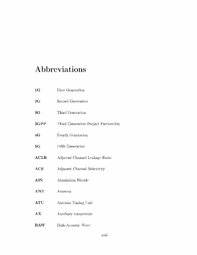
Abbreviations
1G First Generation
2G Second Generation
3G Third Generation
3GPP Third-Generation Project Partnership
4G Fourth Generation
5G Fifth Generation
ACLR Adjacent Channel Leakage Ratio
ACS Adjacent Channel Selectivity
AlN Aluminium Nitride
ANT Antenna
ATU Antenna Tuning Unit
AX Auxiliary transmitter
BAW Bulk-Acoustic Wave
xxii
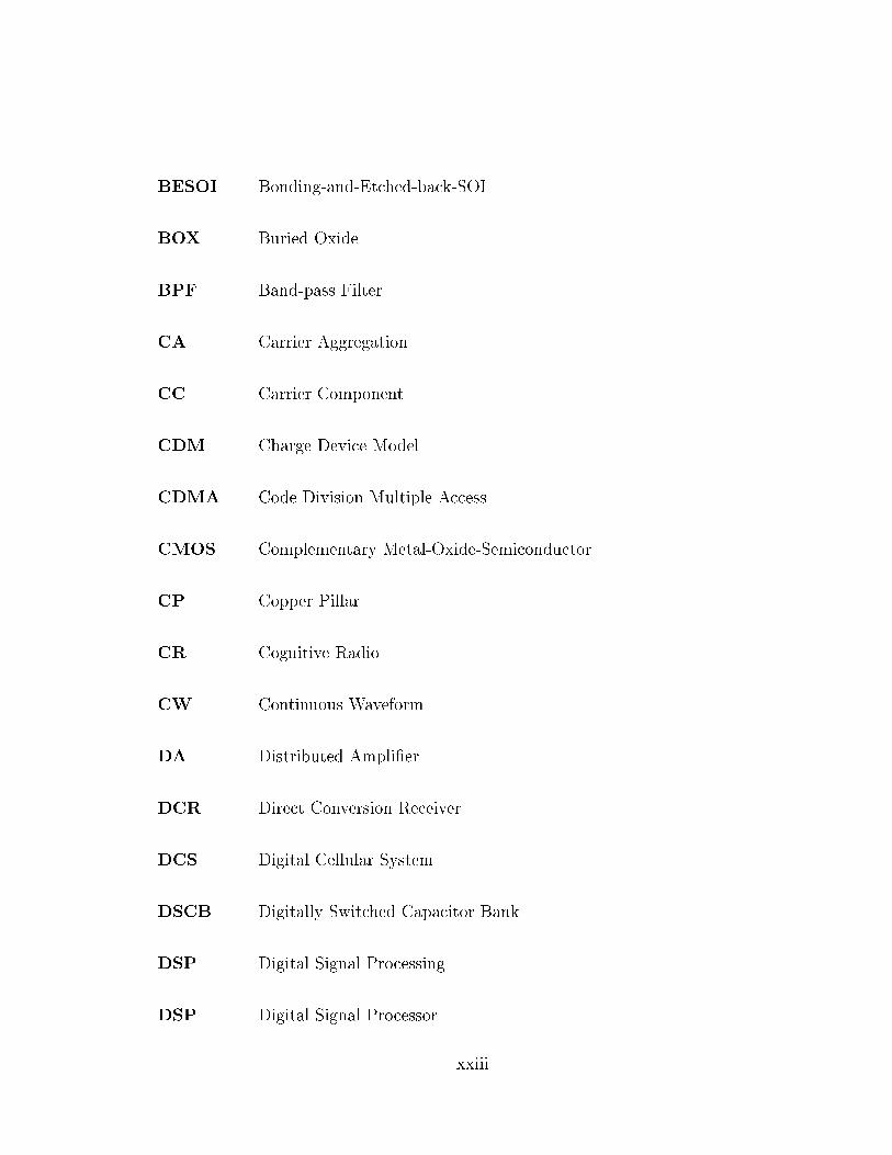
BESOI Bonding-and-Etched-back-SOI
BOX Buried Oxide
BPF Band-pass Filter
CA Carrier Aggregation
CC Carrier Component
CDM Charge Device Model
CDMA Code Division Multiple Access
CMOS Complementary Metal-Oxide-Semiconductor
CP Copper Pillar
CR Cognitive Radio
CW Continuous Waveform
DA Distributed Amplier
DCR Direct Conversion Receiver
DCS Digital Cellular System
DSCB Digitally Switched Capacitor Bank
DSP Digital Signal Processing
DSP Digital Signal Processor
xxiii
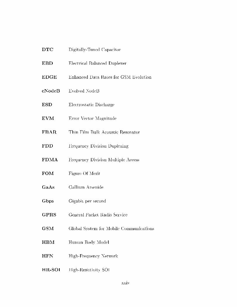
DTC Digitally-Tuned Capacitor
EBD Electrical Balanced Duplexer
EDGE Enhanced Data Rates for GSM Evolution
eNodeB Evolved NodeB
ESD Electrostatic Discharge
EVM Error Vector Magnitude
FBAR Thin-Film Bulk Acoustic Resonator
FDD Frequency Division Duplexing
FDMA Frequency Division Multiple Access
FOM Figure Of Merit
GaAs Gallium Arsenide
Gbps Gigabit per second
GPRS General Packet Radio Service
GSM Global System for Mobile Communications
HBM Human Body Model
HFN High-Frequency Network
HR-SOI High-Resistivity SOI
xxiv
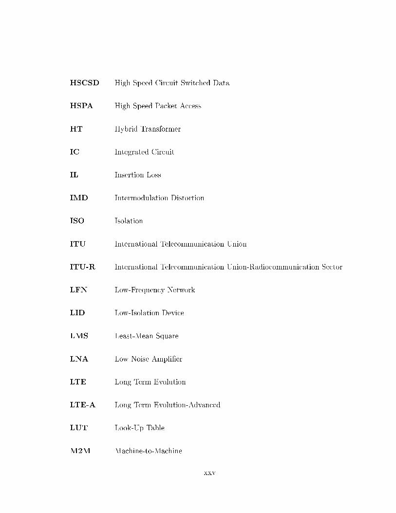
HSCSD High Speed Circuit Switched Data
HSPA High Speed Packet Access
HT Hybrid Transformer
IC Integrated Circuit
IL Insertion Loss
IMD Intermodulation Distortion
ISO Isolation
ITU International Telecommunication Union
ITU-R International Telecommunication Union-Radiocommunication Sector
LFN Low-Frequency Network
LID Low-Isolation Device
LMS Least-Mean Square
LNA Low Noise Amplier
LTE Long Term Evolution
LTE-A Long Term Evolution-Advanced
LUT Look-Up Table
M2M Machine-to-Machine
xxv
Mbps Megabit per second
MESFET Metal-Semiconductor Field-Eect Transistor
MIM Metal-Insulator-Metal capacitor
MM Machine Model
MMIC Monolithic Microwave Integrated Circuit
MMS Multimedia Messaging Service
MPW Multi-Project Wafer
OFDMA Orthogonal Frequency-Division Multiple Access
OOB Out-of-Band
PA Power Amplier
PCB Printed Circuit Board
PCS Personal Communications Service
PDK Process Design Kit
PSD Power Spectral Density
QAM Quadrature Amplitude Modulation
QPSK Quadrature Phase Shift Keying
RB Resource Block
xxvi

RF Radio Frequency
RFIC Radio Frequency Integrated Circuit
RFID Radio-Frequency Identication
RFPA Radio Frequency Power Amplier
SAW Surface-Acoustic Wave
SB Solder Ball
SC-FDMA Single-Carrier Frequency-Division Multiple Access
SDR Software Dened Radio
SEM Spectrum Emission Mask
SIMOX Separation by IMplantation of Oxygen
SMS Short Message Service
SOI Silicon-on-Insulator
SOLT Short-Open-Load-Thru
SOS Silicon-on-Sapphire
SP Scattering-Parameter
SP9T Single-Pole Nine-Throw
SPI Serial-to-Parallel Interface
xxvii

STI Shallow Trench Isolation
TDD Time Division Duplexing
TDMA Time Division Multiple Access
TLP Transmission Line Pulse
UE User Equipment
UMTS Universal Mobile Telecommunication System
WCDMA Wideband Code Division Multiple Access
xxviii
Symbols
B Susceptance
BPFRx Receiver band-pass lter
BPFTx Transmitter band-pass lter
Co OFF-Capacitor
Con ON-Capacitor
CWB Parasitic capacitance of bondwire
DR Dynamic Range
fd Duplexing oset
Fr Receiver noise gure
fres Resonant frequency
Ft Transmitter noise gure
G Conductance
IIP3 Input third-order intercept point
ILPA-to-ANT Insertion loss from PA output to Antenna
ILRx Insertion loss in receive band
xxix
ILTx Insertion loss in transmit band
IM2 Second-order non-linearity
IMP Intermodulation Product
IP2 Second-order intercept point
IP3 Third-order intercept point
ISORx Isolation in receive band
ISOTx Isolation in transmit band
ISOTx-Rx Isolation from transmitter to receiver
KB Boltzmann constant
kTB Thermal noise in the reference bandwidth
Ls Self-inductance
LSB Least-Signicant Bit
LWB Parasitic inductance of bondwire
M Mutual inductance
ne Eective stack height
NF Noise Figure
PJam Jamming signal power
PTx,Ant Transmitter power at antenna port
PTx,Leakage Transmitter leakage power
Q Quality-factor
xxx
Qo Quality-factor in the OFF state
Qon Quality-factor in the ON state
r Ohmic-loss
r(t) Transmit signal
RFESENS Reference Sensitivity
RL Load resistance
RLANT Antenna return loss
Ron ON-Resistance
RWB Series resistance of bondwire
S(ω) Scattering-parameter
SINR Signal-to-Interference-plus-Noise Ratio
T Room Temperature
tox Oxide-thickness
V Peak voltage
X Reactance
XMD Cross-modulation distortion
Y Admittance
y(t) Output signal
Z Impedance
z(t) Cancelling signal
xxxi

δ Skin depth
τ Switching Time
ω Angular frequency
∆ Fractional duplex frequency
xxxii

Chapter 1
Introduction
1.1 Background
The popularity of smart phones, cloud computing and the growing market for machine-
to-machine (M2M) communications is fuelling the growth of mobile broadband. More
spectrum is therefore being allocated to mobile services [1]. Today, nearly half the
spectrum below 3.0 GHz has been earmarked for public radio communications some-
where in the world. Unfortunately, for historical reasons, the spectrum allocations
are fragmented, poorly harmonised between dierent countries and no longer large
enough for the ever-increasing broadband data rates. The next wireless standard,
LTE-A (Long Term Evolution-Advanced), calls for data rates of 100Mbps (mobile)
and 1Gbps (xed). Considerable spectrum (up to 100MHz) is required for these ser-
vices, and is not available in any one band. Carrier aggregation (CA), or operation
on two or more bands at once, will be necessary. A future wireless terminal capable
of global roaming would have to handle more than 44 bands, four generations of op-
erating standards, and two duplexing methods and be capable of carrier aggregation.
This is the research challenge.
1

1. INTRODUCTION
1.2 Carrier Aggregation Concept
The Carrier Aggregation (CA) is the key part of LTE-A standard. It was dened
in 3GPP Release 10 and commercial network launches followed in Korea in 2013
[2]. In principle, the CA aggregates multiple carriers to extend the maximum band-
width in the uplink or downlink (or both) directions. Consequently, it increases
the practical data rates, enhances the network capacity, and simplies the trac
management in spectrum usage. The evolution of data rates through the CA is
shown in Fig.1.1. Commercial LTE networks initially supported 100 to 150Mbps
with continuous 20MHz spectrum. However, the data rate is doubled by introducing
the CA and using two 20 MHz channels. CA ultimately enables the combinations
of many carrier components (CC) with bandwidths of less than 20MHz achieving a
maximum aggregated bandwidth of 100MHz, see Fig.1.1. The CA can basically take
150 Mbps
20 MHz
2x2 MIMO
Cat 4
2012
150 Mbps
10+10MHz
2x2 MIMO
Cat 4
2013
300 Mbps
20+20 MHz
2x2 MIMO
Cat 4
2014
450 Mbps
3 CA
2x2 MIMO
Cat 4
2015600 Mbps
4 CA
2x2 MIMO
Cat 4
2016 1 Gbps+
100 MHz and/
or 4x4
Figure. 1.1: Data rate evolution in downlink with the CA.
place both within the frequency band and between frequency bands. Three scenarios
exist: intra-band contiguous and intra-band non-contiguous occurring within the same
frequency band while inter-band non-contiguous occurs between dierent frequency
bands. Intra-band schemes are handled by baseband DSP ltering, while inter-band
scheme is an RF problem. Fig.1.2 illustrates these scenarios for the LTE-Advanced
2

1. INTRODUCTION
standard. Spectrum fragmentation is a key issue and inter-band non-contiguous could
potentially accommodate this issue. Today's LTE transceivers should be able to em-
ulate all three CA scenarios, particularly the inter-band non-contiguous arrangement.
The latter must receive signals on two separated frequency bands simultaneously.
f
Band 1 Band 2
f
Band 1 Band 2
f
Band 1 Band 2
LTE-Advanced eNodeB
Intra-Band, Contiguous
Intra-Band, non-Contiguous
Inter-Band, non-Contiguous
Figure. 1.2: LTE-A carrier aggregation scenarios; Intra-band and inter-band aggre-gation alternatives.(eNodeB means "evolved NodeB". The LTE basestation that hasevolved from the previous (third) generation UMTS.)
Cognitive Radio (CR) schemes also benet from the ability to receive more than
one signal concurrently. Traditionally, this form of wireless communication detects the
occupied and vacant channels by means of inserting blank periods in the transmission,
allowing CR users to sense for un-occupied channels and instantly move between them.
Thus the use of available radio frequency (RF) spectrum is utilised while minimising
interference to the other users. Although the blank periods are useful, they introduce
a loss of throughput. This issue could be avoided if a CR receives on two frequency
bands at once, one is used for receiving data (without blank periods) while the other
3

1. INTRODUCTION
band senses for vacant channels. In this thesis, we will only consider intra-band
contiguous scenario for combined bandwidth between 5MHz (UMTS channel) and
20MHz (LTE channel).
1.3 Software Dened Radio
Software Dened Radio (SDR) was introduced by Mitola in 1995 [3]. It is the key
enabler of CR. The waveforms or the radio parameters such as carrier frequency and
bandwidth, power, modulation and coding scheme are stored for each channel. In
operation, the entire spectrum is initially scanned to identify vacant channels. The
waveform for the selected channel is then generated using digital processing techniques
such as digital ltering, demodulation and coding. The method eectively eliminates
traditional analogue hardware functions and replaces them with software algorithms
which are executed in high-speed Digital Signal Processors (DSPs). The beauty of
the SDR architecture is that it provides the possibility of implementing a multi-mode,
multi-band and multi-functional transceiver in a single device.
In cellular systems, an SDR mobile handset must cover multiple frequency bands
as well as multiple standards such as GSM, WCDMA, and the most recent LTE. Un-
fortunately, the carrier frequencies involved are not suited to DSP implementation,
thus, this necessitates that the few remaining RF functions of an SDR must be fea-
tured as multi-band components. This a signicant issue since these components are
often xed frequency devices, hence, they operate at a single frequency and cannot
be tuned. In order to cover a wide range of frequency bands, multiple components
are therefore required, resulting in substantial cost.
1.4 Duplexing
Duplexing is required for the simultaneous transmission and reception of signals which
is required for voice and other multimedia applications. Today's wireless terminals
4

1. INTRODUCTION
UL
DLGuard Frequency
RXf
TXf
FDD ModeUL: UplinkDL:Downlink
Base Station
Time
Freq
uenc
y Mobile Terminal
Base Station
Time
Freq
uenc
y
TDD Mode
Mobile Terminal
UL DL DL DL DL UL
Guard Period
/TX RXf
Figure. 1.3: Duplexing modes used in modern mobile communication systems.
are a mixture of software radio baseband circuits running on digital signal processing
(DSP) cores and an analogue circuit that does the up/down conversion to radio
frequency (RF). The RF signal is switched through an appropriate o-chip duplexing
network before reaching the antenna. There are two types of duplexing in use today;
time division duplexing (TDD), where the base-station and terminal transmit in turn,
and frequency division duplex (FDD) where simultaneous transmission occurs, see
Fig.1.3. FDD operation is used by about 90% of handsets (100% in Australia) and is
the subject of this thesis.
FDD uses two closely spaced sub-bands for simultaneous up-link transmission
(talk) and down-link reception (listen). The problem is that the transmitter power
amplier (PA) amplies both the desired transmitter (Tx) signal as well as the noise
over a wide frequency range. Some of this noise falls in the receiver (Rx) band
and desensitises the receiver. Duplex lters separate out the Tx and Rx frequencies
5

1. INTRODUCTION
(Fig.1.4). They need to provide about 50dB isolation between the strong Tx sig-
nal and the sensitive receiver circuits. The band pass lter in the transmitter path
(BPFTx) passes the Tx signal through to the antenna but stops the transmitter noise
(at the receive frequency). The bandpass lter in the receiver path (BPFRx) allows
the incoming Rx signal to enter the receiver but stops the strong Tx signal from over-
loading (blocking) the receiver circuits. The lters are implemented in SAW (surface
acoustic wave) or BAW (Bulk Acoustic Wave) technologies. They are expensive ex-
ternal components in a radio communications solution. Today's terminal has three
to ve duplexers, so when the phone roams to another country, not all bands will be
supported and there is reduced capability, or sometimes no capability.Some thirty-one
duplexers! would be needed for global coverage of all the FDD bands specied by the
International Telecommunications Union (ITU).
Switch
Rx
TxPA
PA
TDD
Tx/Rx
IC
FDD
Rx Filters
Duplex Filters
(a)
Txf
Rxf
df
f
uplink (UL)
channels
Downlink
channels
Duplexing offset
mid-band
gap
BPFTx BPFRx
(b)
Figure. 1.4: Multi-band RF front-end solution: (a) using number of switched duplex-ers (b) using an adaptive duplexer with a low-isolation device (LID) and an activecancellation unit.
6
1. INTRODUCTION
1.5 Adaptive Duplexers
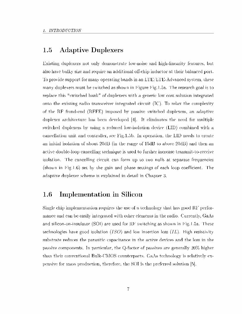
Existing duplexers not only demonstrate low-noise and high-linearity features, but
also have bulky size and require an additional o-chip inductor at their balanced port.
To provide support for many operating bands in an LTE/LTE-Advanced system, these
many duplexers must be switched as shown in Figure Fig.1.5a. The research goal is to
replace this "switched bank" of duplexers with a generic low cost solution integrated
onto the existing radio transceiver integrated circuit (IC). To relax the complexity
of the RF frond-end (RFFE) imposed by passive switched duplexers, an adaptive
duplexer architecture has been developed [4]. It eliminates the need for multiple
switched duplexers by using a reduced low-isolation device (LID) combined with a
cancellation unit and controller, see Fig.1.5b. In operation, the LID needs to create
an initial isolation of about 20dB (in the range of 15dB to above 20dB) and then an
active double-loop cancelling technique is used to further increase transmit-to-receive
isolation. The cancelling circuit can form up to two nulls at separate frequencies
(shown in Fig.1.6) set by the gain and phase settings of each loop coecient. The
adaptive duplexer scheme is explained in detail in Chapter 3.
1.6 Implementation in Silicon
Single chip implementation requires the use of a technology that has good RF perfor-
mance and can be easily integrated with other elements in the radio. Currently, GaAs
and silicon-on-insulator (SOI) are used for RF switching as shown in Fig.1.5a. These
technologies have good isolation (ISO) and low insertion loss (IL). High resistivity
substrate reduces the parasitic capacitance in the active devices and the loss in the
passive components. In particular, the Q-factor of passives are generally 20% higher
than their conventional Bulk-CMOS counterparts. GaAs technology is relatively ex-
pensive for mass production, therefore, the SOI is the preferred solution [5].
7
1. INTRODUCTION
BPFTx
BPFRx
Du
plexer 1
BPFTx
BPFRx
BPFTx
BPFRx
Du
plexer N
RF Switch Du
plexer 2
RF Switch
RF Switch
Tx
Rx
Rxf
Txf
(a)
RxfTxf
LIDCancellation
UnitCanceller
Control
Tx
Rx
Active C
ancellatio
n U
nit
(b)
Figure. 1.5: Multi-band RF front-end solution: (a) using number of switched duplex-ers (b) using an adaptive duplexer with a low-isolation device (LID) and an activecancellation unit.
1.7 Research Goals
The aim of this research is to study the feasibility of implementing the LID as tunable
lters in a variety of media, namely on-chip and discrete (PCB). Two simple band-pass
8
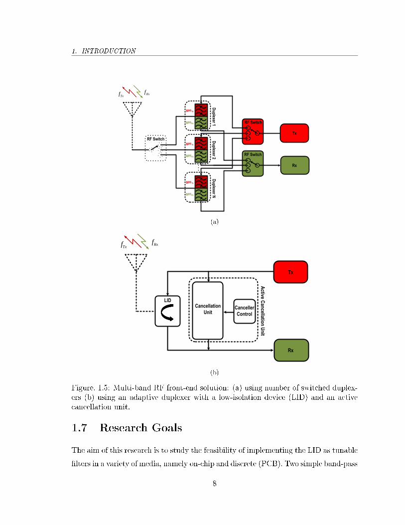
1. INTRODUCTION
Power
f
Tx Noise
Rx Noise
Rx Signal
Tx Leakage Signal
Txf
Rxf
Duplexing
Offset
Adaptive Duplexer
Frequency Response
Figure. 1.6: Spectrum of the transmitter output (red), the receiver input (green) andthe frequency response of the cancelling loops (black) required to cancel both thestrong Tx signal and Tx noise in the vicinity of the received signal.
band-stop structures will be considered, their performance in terms of Q-factor and
tunability will be analysed, and the pros and cons of the dierent implementation
alternatives will be discussed. More specically the main goals of this work are
summarised:
• To identify the specications and design requirements for the LID based on
existing cellular standards. This includes frequency range, channel bandwidth,
duplexing oset (Fig.1.6), power handling, isolation (ISO) and insertion loss
(IL).
• To demonstrate a proof of concept for a single cellular band. LTE band 1 is
targeted here.
• To extend the design for multi-band operation e.g. LTE 1, LTE 2, and LTE 3.
9

1. INTRODUCTION
• To fabricate the above on-chip designs using SOI technologies.
• To improve the performance by using a hybrid solution of high-Q inductors
combined with discreet tunable capacitors on a PCB.
1.8 Research Contributions
The research has led to the following publications:
1. M. Pourakbar, M. Törmänen, H. Sjöland, D. Nobbe, M. Faulkner, " Frequency-
Agile LC Duplex Filter for Adaptive CMOS Duplexer," Submitted to IEEE
Transaction on Circuits and Systems II: Express Briefs, Dec. 2014.
2. M. Pourakbar, R. Eslampanah, M. Faulkner, M. Törmänen, H. Sjöland, "An
SDR Duplex Filter in SOI Technology," in Proc. 1st Australian Microwave
Symposium (AMS), Jun. 2014.
3. R. Eslampanah, M. Pourakbar, S. Ahmed, J.M. Redoute, and M. Faulkner,
"RF Modulator Design for a Low Level Pilot Sub-System," in Proc. 1st Aus-
tralian Microwave Symposium (AMS), Jun. 2014.
4. M. Pourakbar, L. Linton, F. Rivet, M. Faulkner, "Studies on die-to-substrate
interconnects for High-Q PCB inductors," in Proc. IEEE 20th International
Conference on Electronics, Circuits, and Systems (ICECS), pp.633-636, Dec.
2013.
5. M. Pourakbar, M. Törmänen, M. Faulkner, H. Sjöland, "An LC-based tunable
low-isolation device for adaptive duplexers," in Proc. NORCHIP, 2013, pp.1-4,
Nov. 2013.
6. M. Pourakbar, L. Linton, M. Törmänen, and M. Faulkner, "Tunable duplex
lter for adaptive duplexers of advanced LTE handsets," in IEEE MTT-S In-
ternational Microwave Symposium Digest, pp.1-4, Jun. 2013.
10

1. INTRODUCTION
7. M. Pourakbar, R. Amirkhanzadeh, M. Törmänen, J. M. Redoute, and M.
Faulkner, "High Power and High Performance RF SOS FET Switches," in Proc.
GigaHertz Symposium, pp.65, Mar. 2012.
8. R. Amirkhanzadeh, M. Pourakbar, J. M. Redoute, and M. Faulkner, "De-
sign Considerations for Switched Passive Circuits on Silicon-on-Sapphire (SOS)
Process Technology," in Proc. 17th Asia and South Pacic Design Automation
Conference (ASP-DAC), Feb. 2012.
9. M. Pourakbar, J. M. Redoute, and M. Faulkner, "Design and implementation
of high power, high linearity stacked RF FET switches in a 250-nm silicon on
sapphire process," in Proc. IEEE Asia-Pacic Microw. Conference (APMC),
pp.299-302, Dec. 2011.
1.9 Contents and Organisation of the Thesis
This thesis is organised in seven chapters. A brief description of each chapter is
outlined below:
• Chapter 2 outlines the background of this research focusing on cellular standards
and the implications on the RF design aspects of FDD transceiver. It overviews
the key issues associated with the duplexing such as receiver desensitisation and
blocking.
• Chapter 3 surveys the current duplexer structures as used in today's handsets
based on RF ltering. The chapter then continues to overview the alternative
duplexing architectures proposed by the research community. Passive and adap-
tive techniques are emphasised. The latter concentrates on cancelling techniques
which require an LID, the main target of the thesis.
• Chapter 4 is the main theoretical contribution of the work. It introduces
11

1. INTRODUCTION
two types of notch lter so called "Low-Frequency Network (LFN) and High-
Frequency Network (HFN) lters", utilised in the LID.
• Chapter 5 briey reviews the Silicon-on-Insulator (SOI) and the Silicon-on-
Sapphire (SOS) processes, and their features as well as available active and
passive devices for Analog/RF functions. The chapter also briey explains the
RF switching performance of SOI/SOS process.
• Chapter 6 presents an on-chip silicon solution followed by the experimental
results of the SOS prototype. It is also concerned with improving the IL and
the ISO by employing the second proposed conguration of the LFN lter. An
o-the-shelf prototype of a tunable duplex lter is demonstrated as a proof of
concept. This is the main practical contribution of the thesis.
• Chapter 7 demonstrates two fully-integrated solutions for the LID. The lters
cover multiple LTE frequency bands. SOI and SOS processes are chosen for the
implementation. Simulation results are provided.
• Finally, Chapter 8 summarises the measured results for both integrated and
discrete duplex lter solutions. It also gives direction for potential future work.
12

Chapter 2
Background Information
In this Chapter, the RF design requirements and challenges of LTE transceivers in
handsets are presented. Section 2.1 contains a brief history of cellular systems and
their specications from 1G to 4G. LTE frequency bands and a simplied 4G/LTE
transceiver architecture are provided in Section 2.2 and Section 2.3, respectively. The
main RF requirements related to user equipment (UE) for an LTE transmitter and
receiver are described in Section 2.4. In Section 2.5, the minimum requirements
are employed to derive the minimum duplexer isolation for LTE-FDD transceivers.
Finally, a summary is provided in Section 2.6.
2.1 Cellular Systems
The rapid expansion of mobile communication has been hindered by the existence of
a variety of standards used in cellular systems as shown in Fig.2.1. The rst gener-
ation (1G) of cell phones was introduced by Motorola in mid-80's operating in the
450MHz frequency band. It was designed for voice communications which is essen-
tially an analogue system. Frequency Division Multiple Access (FDMA) was used
to provide a number of orthogonal channels for multiple access. The 1G system had
numerous issues such as lack of security in speech transmission, low quality speech
13
2. BACKGROUND INFORMATION
Year of availability
Max
.
Use
r D
ata
Rat
e
Early
1980s
10kbps
1G
AMPS, TACS
NMT450,
NMT 900
1992
14.4kbps
2G
GSM, IS-54
PDC, IS-95
1996
144kbps
2.5G
GSM-EDGE
1999
14Mbps
3G
UMTS
2010
20-100Mbps
4G
LTE
2020
will be
announced
5G
Figure. 2.1: History of cellular communication standards.
due to cross-talk between co-channel users, no roaming capability across the globe
because of hardware incompatibilities, and a limited number of users per communi-
cation channel. In 1992, digital transmission opened a new horizon and the second
generation (2G) was launched. Global System for Mobile potentially increased the
number of subscribers by reducing the reuse distance between co-channel users. GSM
(Global System for Mobile Communications) is a combined FDMA and TDMA (Time
Division Multiple Access) system. GSM is still in operation and uses three frequency
bands: 900 MHz (GSM900), 1800MHz (DCS1800) and 1900MHz (PCS1900). The
low data rate makes this standard suitable for voice, or simple services such as SMS
and MMS. However, demand for new and faster data services was soon acknowledged
and the GSM standard was equipped with new features like HSCSD (High Speed Cir-
cuit Switched Data), GPRS (General Packet Radio Service) and EDGE (Enhanced
14

2. BACKGROUND INFORMATION
Data Rates for GSM Evolution). In 1999, the third Generation Partnership Project
(3GPP) unied the telecommunication standards and released third generation (3G)
cellular network known as Universal Mobile Telecommunications System (UMTS) [6].
It was based on the spread spectrum approach and multiple access technology referred
to as Wideband Code Division Multiple Access (WCDMA), which allows all users of
the same network to use the same frequency band simultaneously. UMTS adjusts its
output power according to the distance between handset and base-station, in order
to reduce interference and save energy. Packet transmission techniques allow it to be
constantly connected to the Internet and its high spectral eciency makes it 2 to 3
times more ecient than GSM.
Further demand for mobile networks oering mobile Internet services as fast as
xed home internet services led to the introduction of the fourth generation (4G)
Long-Term Evolution (LTE) standard in 2010. It allows maximum user data rates of
100Mbps downstream and 50Mbps upstream, while reducing the cost per Megabit of
data transport. Recent achievements have demonstrated that greater data bandwidth
of 400Mbps could be obtained by aggregating up to three frequency bands simultane-
ously. LTE uses multicarrier transmission technology, Orthogonal Frequency-Division
Multiple Access (OFDMA) in the downlink, Single-Carrier Frequency-Division Mul-
tiple Access (SC-FDMA) in the uplink, and MIMO transmission. LTE includes the
previous 2G and 3G standards which allows network mobility with a single standard.
Thus, the communication data rate will be optimized depending on the standard im-
plemented within the user's geographic location. Beyond 4G will be 5G with trans-
mission speeds up to 10Gbps. The European Commission has committed to fund the
research with the aim of delivering 5G by 2020 [7].
15
2. BACKGROUND INFORMATION
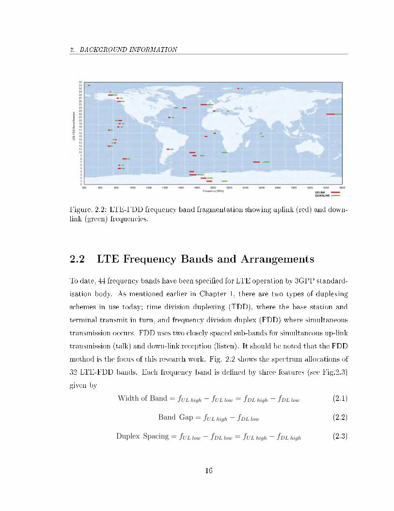
Figure. 2.2: LTE-FDD frequency band fragmentation showing uplink (red) and down-link (green) frequencies.
2.2 LTE Frequency Bands and Arrangements
To date, 44 frequency bands have been specied for LTE operation by 3GPP standard-
isation body. As mentioned earlier in Chapter 1, there are two types of duplexing
schemes in use today; time division duplexing (TDD), where the base station and
terminal transmit in turn, and frequency division duplex (FDD) where simultaneous
transmission occurs. FDD uses two closely spaced sub-bands for simultaneous up-link
transmission (talk) and down-link reception (listen). It should be noted that the FDD
method is the focus of this research work. Fig. 2.2 shows the spectrum allocations of
32 LTE-FDD bands. Each frequency band is dened by three features (see Fig.2.3)
given by
Width of Band = fUL high − fUL low = fDL high − fDL low (2.1)
Band Gap = fUL high − fDL low (2.2)
Duplex Spacing = fUL low − fDL low = fUL high − fDL high (2.3)
16
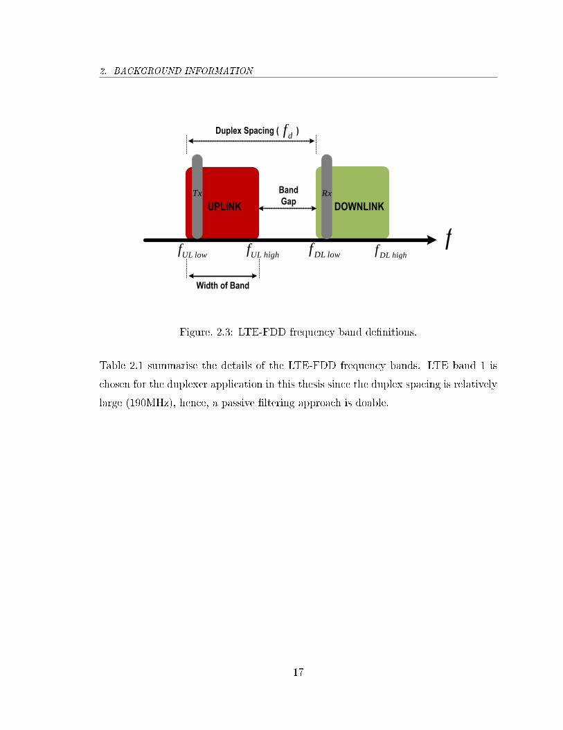
2. BACKGROUND INFORMATION
fDL low
fDL high
fUL lowf UL high
f
UPLINK DOWNLINK
Band
Gap
Width of Band
Duplex Spacing ( )d
f
Tx Rx
Figure. 2.3: LTE-FDD frequency band denitions.
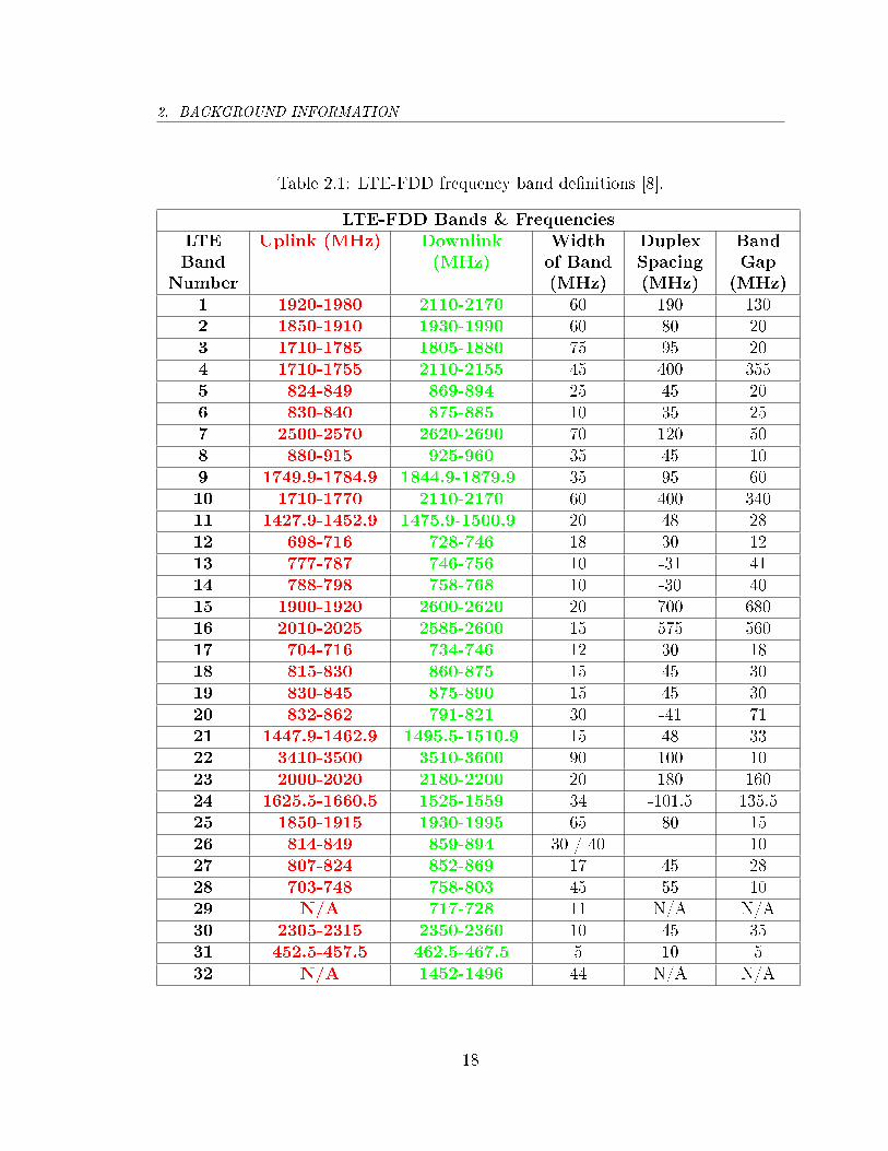
Table 2.1 summarise the details of the LTE-FDD frequency bands. LTE band 1 is
chosen for the duplexer application in this thesis since the duplex spacing is relatively
large (190MHz), hence, a passive ltering approach is doable.
17
2. BACKGROUND INFORMATION
Table 2.1: LTE-FDD frequency band denitions [8].
LTE-FDD Bands & FrequenciesLTEBand
Number
Uplink (MHz) Downlink(MHz)
Widthof Band(MHz)
DuplexSpacing(MHz)
BandGap(MHz)
1 1920-1980 2110-2170 60 190 1302 1850-1910 1930-1990 60 80 203 1710-1785 1805-1880 75 95 204 1710-1755 2110-2155 45 400 3555 824-849 869-894 25 45 206 830-840 875-885 10 35 257 2500-2570 2620-2690 70 120 508 880-915 925-960 35 45 109 1749.9-1784.9 1844.9-1879.9 35 95 6010 1710-1770 2110-2170 60 400 34011 1427.9-1452.9 1475.9-1500.9 20 48 2812 698-716 728-746 18 30 1213 777-787 746-756 10 -31 4114 788-798 758-768 10 -30 4015 1900-1920 2600-2620 20 700 68016 2010-2025 2585-2600 15 575 56017 704-716 734-746 12 30 1818 815-830 860-875 15 45 3019 830-845 875-890 15 45 3020 832-862 791-821 30 -41 7121 1447.9-1462.9 1495.5-1510.9 15 48 3322 3410-3500 3510-3600 90 100 1023 2000-2020 2180-2200 20 180 16024 1625.5-1660.5 1525-1559 34 -101.5 135.525 1850-1915 1930-1995 65 80 1526 814-849 859-894 30 / 40 1027 807-824 852-869 17 45 2828 703-748 758-803 45 55 1029 N/A 717-728 11 N/A N/A30 2305-2315 2350-2360 10 45 3531 452.5-457.5 462.5-467.5 5 10 532 N/A 1452-1496 44 N/A N/A
18
2. BACKGROUND INFORMATION
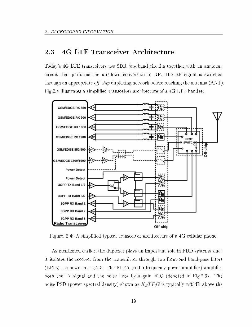
2.3 4G LTE Transceiver Architecture
Today's 4G LTE transceivers use SDR baseband circuits together with an analogue
circuit that performs the up/down conversion to RF. The RF signal is switched
through an appropriate o-chip duplexing network before reaching the antenna (ANT).
Fig.2.4 illustrates a simplied transceiver architecture of a 4G LTE handset.
PA
PA
PA
PA
PA
GSM/EDGE RX 850
GSM/EDGE RX 900
GSM/EDGE RX 1800
GSM/EDGE 850/900
GSM/EDGE 1800/1900
Power Detect
Power Detect
3GPP TX Band 1/2
3GPP TX Band 5/6
3GPP RX Band 1
3GPP RX Band 2
3GPP RX Band 5
PA
PA
PA
PA
LNA
LNA
LNA
LNA
LNA
LNA
SP9T
SWITCH
GSM/EDGE RX 1900 LNA
Off-chip
Off
-ch
ip
Radio Transceiver
Figure. 2.4: A simplied typical transceiver architecture of a 4G cellular phone.
As mentioned earlier, the duplexer plays an important role in FDD systems since
it isolates the receiver from the transmitter through two front-end band-pass lters
(BPFs) as shown in Fig.2.5. The RFPA (radio frequency power amplier) amplies
both the Tx signal and the noise oor by a gain of G (denoted in Fig.2.6). The
noise PSD (power spectral density) shown as KBTFtG is typically ≈35dB above the
19

2. BACKGROUND INFORMATION
receiver noise oor (KBTFr). BPFTx attenuates the transmitter wideband noise PSD
at the Rx frequency band which would eventually avoid the increase of receiver noise
gure, see Fig.2.6. On the other hand, BPFRx prevents the strong transmit signal
leaking into the Rx path causing receiver desensitisation and blocking the receive
signal as shown in Fig.2.7.
BPFTX
RFPA
RXfTX
f
Duplexer
BPFRXLNA
ʎ/4
TXf RX
fd
f
f
BPFTX BPFRX
Figure. 2.5: Conventional duplexer consists of two front-end BPFs.
PSD
G
B tK TF G
B tK TF
B rK TF
Txf
Rxf
BPFTx
f
BPFTx
BPFRx
G+Modulator
Upconverter
Rx
B tK T F
Du
plexer
Tx
Tx Noise
PSD: Power Spectral Density
KB: Boltzmann constant
T: Room temperature
Ft: Transmitter noise figure
Fr: Receiver noise figure
G: Amplifier gain
Figure. 2.6: Transmitter noise in the Rx band is attenuated by BPFTx.
20

2. BACKGROUND INFORMATION
BPFTx
BPFRx
+Rx
B rK T F
Du
plexer
Tx
Tx Leakage Signal
LNA
PSD
Max. Rx Signal (overload level)
B rK TF
Txf
Rxf
BPFRx
f
PSD: Power Spectral Density
KB: Boltzmann constant
T: Room temperature
Ft: Transmitter noise figure
DR: Dynamic Range
DR
Figure. 2.7: Receiver desensitisation due to overload by the Tx signal unless attenu-ated by BPFRx.
Rxf
Txf
BPFTx BPFRx
Duplexer
RFPA
Tx Signal
PTx
LNA
Tx Leakage
Desired
Signal
PRx
In-band
Jammer
Tx
Leakage
PTx,Leakage
Desired
Signal
PRx
In-band
JammerPJam
Cross-Modulation
Tx
Leakage
Desired
Signal
Figure. 2.8: Cross-modulation distortion eect due to the strong Tx leakage.
2.3.1 Impact of Tx Leakage on the Receiver
The high power Tx signal can desensitise the receiver through several mechanisms.
First, the transmitter noise leakage in the receive band is added to the Rx noise oor
unless adequate Tx-Rx isolation is obtained by the duplexer at the Rx band.
Second, cross-modulation distortion (XMD) between the transmitter leakage and
a jamming signal can potentially overlap in frequency with the wanted signal as shown
in Fig.2.8. Using the Taylor series power expansion for the receiver non-linearity, the
21

2. BACKGROUND INFORMATION
generated XMD can be calculated as
XMD(dBm) = PJam (dBm) + 2 PTx,Leakage (dBm)− 2 IIP3 (dBm) (2.4)
where IIP3 is the 3rd order input intercept point. (2.4) indicates that every 10dB
Rxf
Txf
BPFTx BPFRx
Duplexer
RFPA
Tx Signal
PTx Desired Signal
PRx
Tx
Leakage
PTx,Leakage
Desired
Signal
PRx
LNA
LO
0
2nd order
distortionTx Leakage
Figure. 2.9: Second-order nonlinearity eect due to the strong Tx leakage.
improvement in duplexer isolation results in a 20dB improvement of the XMD.
Third, in a direct conversion receiver (DCR), self-mixing of the Tx leakage signal
causes second-order non-linearity (IM2) products at baseband, see Fig.2.9. The IM2
can be characterised by the 2nd order intercept point (IP2). Two equal-amplitude RF
tones are applied at the input and the resultant IM2 products are observed at the
output. IP2 can then be obtained by extrapolating the plotted fundamental tone and
the IM2 product versus the input power. For instance, a two-tone Tx leakage signal
generates the IM2 product given by
IM2(dBm) ≈ 2 PTx,Leakage (dBm)− IIP2 (dBm)− 6 dB (2.5)
where IIP2 is the second order input intercept point and the 6dB factor is used when
two-tones with half of the Tx leakage power are applied.
Finally, LO phase noise can produce reciprocal mixing with the Tx leakage signal
that falls in the Rx band (particularly when the duplex oset is low) as illustrated
22
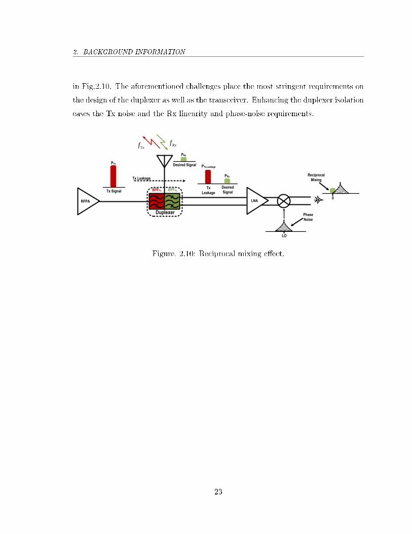
2. BACKGROUND INFORMATION
in Fig.2.10. The aforementioned challenges place the most stringent requirements on
the design of the duplexer as well as the transceiver. Enhancing the duplexer isolation
eases the Tx noise and the Rx linearity and phase-noise requirements.
Rxf
Txf
BPFTx BPFRx
Duplexer
RFPA
Tx Signal
PTx Desired Signal
PRx
Tx
Leakage
PTx,Leakage
Desired
Signal
PRx
LNA
Tx Leakage
LO
Phase
Noise
0
Reciprocal
Mixing
Figure. 2.10: Reciprocal mixing eect.
23

2. BACKGROUND INFORMATION
2.4 LTE UE Transceiver Design Requirements
In 4G handsets, LTE functionality is included into the existing the 2G GSM/EDGE
and 3.5G WCDMA/HSPA architecture. The main design requirements related to
the LTE UE transmitter and the receiver are described in this section. Further
information may be obtained from the 3GPP technical documents [8, 9].
2.4.1 RF Transmitter Requirements
LTE transmitters must satisfy two general sets of requirements: one related to the
power level and modulation accuracy of the intended transmitted signal (known as
signal quality), and the other related to the level of unwanted emissions.
2.4.1.1 Intended Transmission Requirements
• UE Transmit Output Power
The LTE UE power class depends on the operating band. It is dened as the
maximum output power for Quadrature Phase Shift Keying (QPSK) modulation
at the antenna port. The main UE power class is set to 23dBm with a tolerance
of ±2dB for all bands [8].
• Signal Quality
The transmitted UE signal deviates from an ideal modulated signal due to
RF imperfections in the transmitter mainly caused by the non-linearity of the
PA. The signal quality is measured by the Error Vector Magnitude (EVM)
of the modulated signal constellation. It fundamentally denes the maximum
SNR that can be achieved at the receiver when the channel is ideal and noise-
less. The EVM requirement in LTE relates to the modulation scheme. The
LTE 64 Quadrature Amplitude Modulation (64QAM) places the most stringent
requirement on the EVM budget being less than 8%. However, 16 Quadrature
24

2. BACKGROUND INFORMATION
Amplitude Modulation (16QAM) and QPSK are required to meet EVM budgets
of 12.5% and 17.5%, respectively [8].
2.4.1.2 Unwanted Emission Requirements
The ITU-R recommendation classies unwanted emissions from the transmitter into
two categories, Out-of-Band (OOB) emissions and spurious emissions as shown in
Fig.2.11. Intermodulation in the PA causes OOB emissions in adjacent channels,
while spurious emissions occur outside the RF carrier region. The boundary between
the OOB and spurious domains is dened by ITU-R at a frequency separation from
the RF carrier of 2.5 times channel bandwidths.
RBs
Channel
Bandwidth∆fOOB ∆fOOB
LTE Band
Spurious Emission
Region
Spurious Emission
Region
Frequency
Figure. 2.11: LTE transmitter spectrum [8]. (RBs: Resource Blocks).
• Out-of-Band Emissions
Since OOB emissions are generated by the PA non-linearity, decreasing the
transmit power will reduce these undesired signals. The bandwidth of LTE
system is not xed; it is more practical to consider the OOB requirement to
25

2. BACKGROUND INFORMATION
Figure. 2.12: SEM for a UE transmitter for various LTE channel bandwidths [8].
the edge of the channel bandwidth compared to that of measured to the centre
frequency of the channel in UMTS radio. Here, two overlapping requirements
are dened: Spectrum Emission Mask (SEM) and Adjacent Channel Leak-
age Ratio (ACLR). SEM species the maximum permissible OOB emissions
in dBm/MHz outside of the necessary channel bandwidth. Fig.2.12 illustrates
the SEMs for dierent LTE channel bandwidths. The ACLR measures the un-
wanted fraction of signal power falling in the neighbouring radio channel as
per Fig.2.13. It should be noted that the increase in ACLR is mostly due to
occupancy of the adjacent channel by the 3rd and 5th order intermodulation
distortion (IMD) products.
The ACLR of handsets is set to be <-30dBc for an adjacent 20MHz LTE
channel, and <-33dBc for adjacent UMTS channel measured at 5MHz of the
OBB spectrum and <-36dBc for the second adjacent UMTS channel found
10MHz separated from the desired channel.
26

2. BACKGROUND INFORMATION
Wanted
Signal
Frequency
Aggressor
Ratio defines the ACLR for
transmitted (aggressor) signal
Transmitter
unwanted emissions
Figure. 2.13: Illustration of ACLR for two nearby radio channels.
• Spurious Emissions
Spurious emissions are mainly due to unwanted transmitter eects such as har-
monic emissions, parasitic emissions, intermodulation and frequency conversion
products. Table 2.2 shows the spurious emission requirements for the UE. In
FDD systems, the spurious emissions can fall in the receive channel blocking the
weak wanted receive signal. Hence, the spurious requirement is very stringent in
this part of the spectrum. In LTE, the spurious emissions must be <-130dBc/Hz
at the maximum transmit power of 23dBm for a mobile terminal.
Table 2.2: UE LTE spurious emission requirements [9].
Frequency Range MaximumLevel
MeasurementBandwidth
Note
9kHz≤ f < 150kHz -36dBm 1kHz150kHz≤ f < 30MHz -36dBm 10kHz30MHz≤ f < 1000MHz -36dBm 100kHz1.0GHz≤ f < 12.75GHz -36dBm 1MHz12.75GHz≤ f < 5th
harmonic of the upperfrequency edge of the ULoperating band in GHz
-30dBm 1MHz 1
NOTE 1: Applies for Band 22, Band 42, and Band 43
27
2. BACKGROUND INFORMATION
2.4.2 RF Receiver Requirements
In this sub-section, two main requirements are highlighted: receiver sensitivity and
dynamic range, and receiver susceptibility to interfering signals.
2.4.2.1 Sensitivity Level and Dynamic Range
The LTE receiver should detect a weak wanted signal. The reference sensitivity (REF-
SENS) of a receiver is the minimum received signal strength required to guarantee
a throughput of 95% of maximum throughput (for a given modulation and coding
scheme). Practically, RFESENS is given by
REFSENS = kTB +NF + SINR + IM − 3 (dBm) (2.6)
where kTB is the thermal noise in the reference bandwidth, NF is maximum overall
noise gure of the receiver, SINR is selected based on the applied modulation and
coding scheme, IM is the implementation margin which is 2.5dB for QPSK 1/3 and
4dB for 64QAM 3/4, and -3dB is added for the diversity gain. Table.2.3 shows the
REFSENS requirement for a UE at dierent channel bandwidths. The measurement
assumes the FDD transmitter is at full power (23dBm).
Table 2.3: REFSENS of UE LTE receiver for Band 1.
ModulationScheme
ChannelBandwidth
kTB(dBm)
NF(dB)
SINR(dB)
IM(dB)
REFSENS(dBm)
QPSK 1/35MHz -107.5 9 -1 2.5 -10020MHz -101.4 9 -1 2.5 -94
64QAM* 3/45MHz -107.5 9 17.5 4 -8020MHz -101.4 9 17.5 4 -74
*The REFSENS is specied for QPSK modulation.
The dynamic range requirement for the receiver ensures that it can operate at an
Rx signal level considerably higher than REFSENS. For the UE, the dynamic range
is dened as the maximum signal level at which the required throughput is achieved
minus (dB scale) the minimum signal level at which the throughput is met [8].
28
2. BACKGROUND INFORMATION
2.4.2.2 Receiver Susceptibility to Interfering Signals
LTE requires handheld devices to receive the wanted signal in the presence of a strong
interfering signal. The receiver sensitivity should not be reduced by more than 0.5dB
when the transmitter operates simultaneously as required in FDD systems. The
receiver selectivity and blocking measures are briey explained below.
• Blocking
There are two types of blockers, one outside the operating band (out-of-band
blocker) and the other inside the operating band (in-band blocker). In both
cases, they are not adjacent to the wanted signal. In LTE, Out-band blockers
are positioned 15MHz or more from the band edge and must be suppressed to
>-44dBm. In-band blockers are severe issues because they cannot be removed by
ltering. Signals as high as -25dBm must be tolerated in the adjacent channel.
• Adjacent Channel Selectivity (ACS)
The ACS is a measure of the receiver's ability to reject signals in the adjacent
channel. It is basically dened by the ratio of the receive lter attenuation on
the assigned channel (passband) to the receive lter attenuation in the adjacent
channel (stopband). According to [9], the required ACS is 33dB for 5MHz
channels and 27dB for a 20MHz channels.
• Narrowband Blocking
Narrowband blockers are unwanted narrowband continuous waveform (CW)
interferers occurring at frequencies less than the nominated channel spacing.
They should be attenuated to -55dBm at least [9].
• Receiver Intermodulation
The intermodulation products are caused by non-linearities and can sometimes
fall in the desired receive band, therefore, they should be less than -94dBm to
be below the receiver sensitivity level of a 5MHz channel.
29

2. BACKGROUND INFORMATION
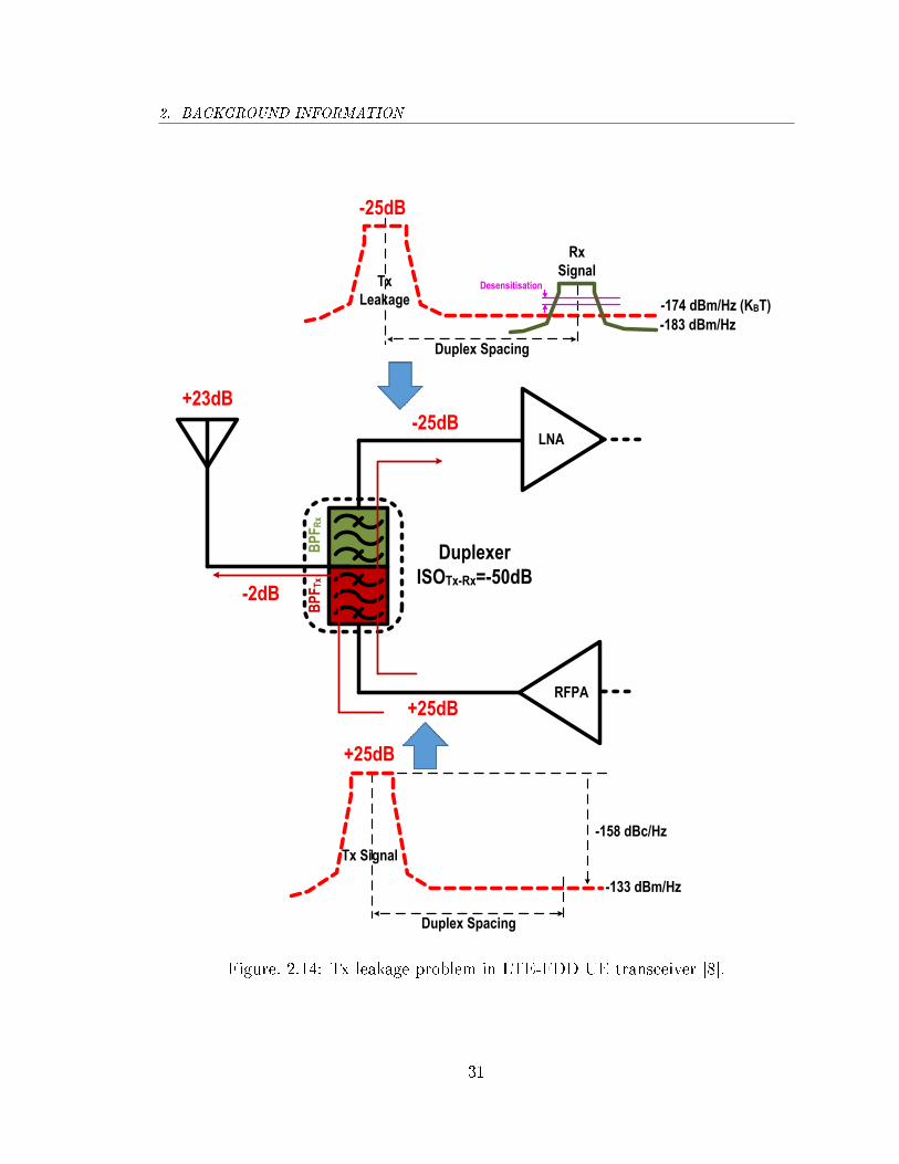
2.5 Typical Duplexer Requirements for LTE
As mentioned in Section 2.3.1, the Tx leakage signal and the Tx leakage noise are two
interferers that can potentially desensitise the receiver. LTE requires the Tx noise
leaking into the Rx band to be <-183dBm/Hz. The Tx leakage signal level is predom-
inantly determined by the ISOTx−Rx. Given the spurious emission level of -107dB/Hz
for the Rx band, the required duplexer isolation of 76dB and 59dB is obtained for LTE
and UMTS, respectively. However, today's RF mobile platform manufacturers have
improved their spurious emissions to a level of -133dBm/Hz resulting in a reduced
isolation requirement ISOTx−Rx ≈50dB. This scenario is illustrated in Fig.2.14. The
Tx leakage power at the receiver input is given by
PTx,Leakage(dBm) = PTx,ANT (dBm) + ILPA−to−ANT (dB)− ISOTx−Rx (dB) (2.7)
where ILPA−to−ANT is the insertion loss from the PA output to the ANT, which
includes the RF switch, duplexer and the PCB routing. ILPA−to−ANT can be as high
as 2dB. In LTE, the maximum PA output power can be 25dBm, resulting in a PTx,ANT
of 23dBm at the antenna port. Assuming a typical duplexer isolation of 50dB, the
receiver will face Tx leakage of -25dBm (23dBm+2dB-50dB), which is just below the
blocking limit of the receiver.
30
2. BACKGROUND INFORMATION
BP
FT
xB
PF
Rx
Duplexer
ISOTx-Rx=-50dB
RFPA
LNA
+25dB
-25dB
+23dB
-2dB
Tx Signal
+25dB
-133 dBm/Hz
-158 dBc/Hz
Duplex Spacing
Tx
Leakage
-25dB
-174 dBm/Hz (KBT)
-183 dBm/Hz
Duplex Spacing
Rx
SignalDesensitisation
Figure. 2.14: Tx leakage problem in LTE-FDD UE transceiver [8].
31

2. BACKGROUND INFORMATION
2.6 Summary
In this chapter, a brief history of cellular standards is given. Nowadays, LTE systems
known as 4G networks are commonly used operating in either the FDD or the TDD
modes. Here, the LTE-FDD is introduced and a simplied transceiver architecture is
shown. Duplexers are the key components used in the FDD transceivers to attenuate
the Tx leakage signal and the Tx leakage noise in the receiver chain. Therefore,
the impact of a high power Tx signal on the receiver are explained with particular
emphasis on cross-modulation, reciprocal mixing, and second-order non-linearities.
The UE RF requirements for the transmitter and the receiver are discussed. Finally,
typical requirements for an LTE duplexer are provided from which it is concluded
that the duplexer isolation must be at least 50dB in both Tx and Rx bands.
This Chapter introduced the basic requirements for the LTE-FDD system em-
phasising the duplexer. The next Chapter reviews the literature on duplexers and
adaptive duplexing methods.
32

Chapter 3
Duplexing Techniques: Literature
Survey
FDD systems use two closely spaced carriers for simultaneous uplink transmission
and downlink reception. We previously explained the potential desensitization of
the receiver by the two strong leakage signals (the Tx leakage and the Tx noise).
Therefore, a 3-terminal component was introduced known as a duplexer that isolates
the receiver from the strong transmitter while allowing them to share the same an-
tenna, see Fig.2.5. In that gure, it is shown that a conventional duplexer consists
of two xed frequency bandpass lters (BPFTx and BPFRx) and a transmission line
which acts as a matching network. As previously described, increasing the number
of operating frequency bands has resulted in the switching of multiple duplexers as a
feasible solution for current handset manufacturers. The duplexer is a bulky compo-
nent which means that putting an array of duplexers into a cellular phone will result
in increased size and cost of the handset. The theory of a circulator-based duplexer is
reviewed in Section 3.1. Section 3.2 introduces passive duplexing methods including
non-tunable lters, separated antennas, directional couplers and hybrid transformers
known as electrical balancing circuits. Active cancellation architectures are discussed
in Section 3.3 and a summary is given in Section 3.4.
33
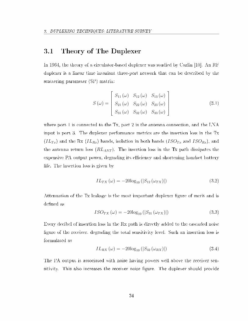
3. DUPLEXING TECHNIQUES: LITERATURE SURVEY
3.1 Theory of The Duplexer
In 1964, the theory of a circulator-based duplexer was studied by Carlin [10]. An RF
duplexer is a linear time invariant three-port network that can be described by the
scattering parameter (SP) matrix:
S (ω) =
S11 (ω) S12 (ω) S13 (ω)
S21 (ω) S22 (ω) S23 (ω)
S31 (ω) S32 (ω) S33 (ω)
(3.1)
where port 1 is connected to the Tx, port 2 is the antenna connection, and the LNA
input is port 3. The duplexer performance metrics are the insertion loss in the Tx
(ILTx) and the Rx (ILRx) bands, isolation in both bands (ISOTx and ISORx), and
the antenna return loss (RLANT ). The insertion loss in the Tx path dissipates the
expensive PA output power, degrading its eciency and shortening handset battery
life. The insertion loss is given by
ILTX (ω) = −20log10 (|S12 (ωTX)|) (3.2)
Attenuation of the Tx leakage is the most important duplexer gure of merit and is
dened as
ISOTX (ω) = −20log10 (|S31 (ωTX)|) (3.3)
Every decibel of insertion loss in the Rx path is directly added to the cascaded noise
gure of the receiver, degrading the total sensitivity level. Such an insertion loss is
formulated as
ILRX (ω) = −20log10 (|S32 (ωRX)|) (3.4)
The PA output is associated with noise having powers well above the receiver sen-
sitivity. This also increases the receiver noise gure. The duplexer should provide
34
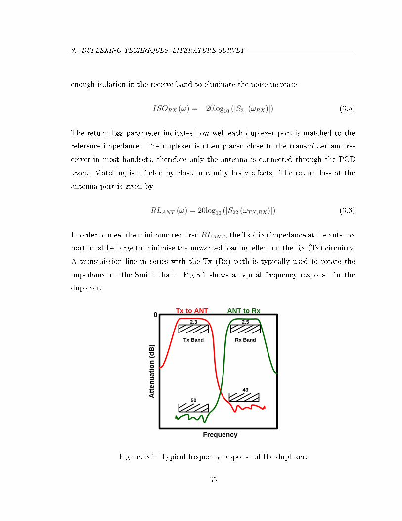
3. DUPLEXING TECHNIQUES: LITERATURE SURVEY
enough isolation in the receive band to eliminate the noise increase.
ISORX (ω) = −20log10 (|S31 (ωRX)|) (3.5)
The return loss parameter indicates how well each duplexer port is matched to the
reference impedance. The duplexer is often placed close to the transmitter and re-
ceiver in most handsets, therefore only the antenna is connected through the PCB
trace. Matching is eected by close proximity body eects. The return loss at the
antenna port is given by
RLANT (ω) = 20log10 (|S22 (ωTX,RX)|) (3.6)
In order to meet the minimum requiredRLANT , the Tx (Rx) impedance at the antenna
port must be large to minimise the unwanted loading eect on the Rx (Tx) circuitry.
A transmission line in series with the Tx (Rx) path is typically used to rotate the
impedance on the Smith chart. Fig.3.1 shows a typical frequency response for the
duplexer.
Tx to ANT ANT to Rx0
Att
en
uati
on
(d
B)
2.3 2.5
43
50
Frequency
Tx Band Rx Band
Figure. 3.1: Typical frequency response of the duplexer.
35
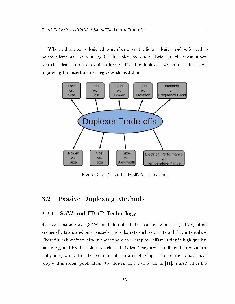
3. DUPLEXING TECHNIQUES: LITERATURE SURVEY
When a duplexer is designed, a number of contradictory design trade-os need to
be considered as shown in Fig.3.2. Insertion loss and isolation are the most impor-
tant electrical parameters which directly aect the duplexer size. In most duplexers,
improving the insertion loss degrades the isolation.
Duplexer Trade-offs
Loss
vs.
Size
Loss
vs.
Cost
Loss
vs.
Power
Loss
vs.
Isolation
Isolation
vs.
Frequency Band
Power
vs.
Size
Cost
vs.
size
Size
vs.
Bandwidth
Electrical Performance
vs.
Temperature Range
Figure. 3.2: Design trade-os for duplexers.
3.2 Passive Duplexing Methods
3.2.1 SAW and FBAR Technology
Surface-acoustic wave (SAW) and thin-lm bulk acoustic resonator (FBAR) lters
are usually fabricated on a piezoelectric substrate such as quartz or lithium-tantalate.
These lters have intrinsically linear phase and sharp roll-os resulting in high quality-
factor (Q) and low insertion loss characteristics. They are also dicult to monolith-
ically integrate with other components on a single chip. Two solutions have been
proposed in recent publications to address the latter issue. In [11], a SAW lter has
36

3. DUPLEXING TECHNIQUES: LITERATURE SURVEY
been mounted on top of a transceiver chip while in [12, 13], an FBAR has been inte-
grated at the wafer level (Fig.3.3). However, these congurations require additional
matching networks and expensive masks and costly procedures in the fabrication
process.
(a)
(b)
(c)
Figure. 3.3: Cross section of (a) stacked SAW lter on a transceiver [11] (b) FBARlter integrated above IC [12] (c) BAW resonator with solder bumps [13].
A low insertion loss and high rejection duplexer using FBAR technology was
developed by Feld et al. [14]. The ladder topologies for both transmitter and receiver
dice have been employed, which contain 3 series- 3 shunt and 3 series-4 shunt topol-
ogy respectively. In addition to the above technique, a quarter wavelength microstrip
transmission line (at the transmit frequency) was used as a phase shifter in the re-
ceiver path (see in Fig.3.4). Although this design approach can meet all the required
specications, the dimension of the chip (3.8mm x 3.8mm x 1.4mm) and cost were
37
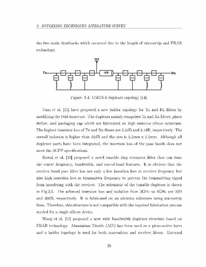
3. DUPLEXING TECHNIQUES: LITERATURE SURVEY
the two main drawbacks which occurred due to the length of microstrip and FBAR
technology.
FBARFBAR
FBAR
FBAR
FBAR
FBAR
FBAR FBARFBAR
FBAR FBAR
FBARFBAR
RxTx
-
-λ/4
Figure. 3.4: UMTS-1 duplexer topology [14].
Nam et al. [15] have proposed a new ladder topology for Tx and Rx lters by
modifying the Feld structure. The duplexer mainly comprises Tx and Rx lters, phase
shifter, and packaging cap which are fabricated on high resistive silicon substrate.
The highest insertion loss of Tx and Rx lters are 2.5dB and 3.1dB, respectively. The
overall isolation is higher than 42dB and the size is 2.5mm x 2.5mm. Although all
duplexer parts have been integrated, the insertion loss of the pass bands does not
meet the 3GPP specications.
Kawai et al. [16] proposed a novel tunable ring resonator lter that can tune
the centre frequency, bandwidth, and out-of-band features. It is obvious that the
receiver band pass lter has not only a low insertion loss at receiver frequency but
also high insertion loss at transmitter frequency to prevent the transmitting signal
from interfering with the receiver. The schematic of the tunable duplexer is shown
in Fig.3.5. The achieved insertion loss and isolation from 3GHz to 4GHz are 2dB
and 30dB, respectively. It is fabricated on an alumina substrate using microstrip
lines. Therefore, this structure is not compatible with the required fabrication process
needed for a single silicon device.
Wang et al. [17] proposed a new wide bandwidth duplexer structure based on
FBAR technology. Aluminium Nitride (AlN) has been used as a piezo-active layer
and a ladder topology is used for both transmitter and receiver lters. External
38
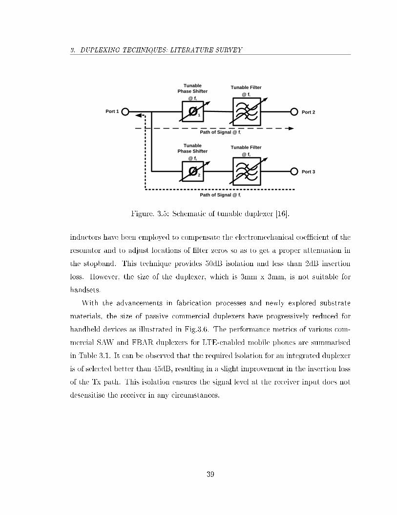
3. DUPLEXING TECHNIQUES: LITERATURE SURVEY
Path of Signal @ f2
Path of Signal @ f1
Tunable Filter
@ f2
Tunable
Phase Shifter
@ f2
Ø2
Tunable Filter
@ f1
Tunable
Phase Shifter
@ f1
Ø1 Port 2
Port 3
Port 1
Figure. 3.5: Schematic of tunable duplexer [16].
inductors have been employed to compensate the electromechanical coecient of the
resonator and to adjust locations of lter zeros so as to get a proper attenuation in
the stopband. This technique provides 50dB isolation and less than 2dB insertion
loss. However, the size of the duplexer, which is 3mm x 3mm, is not suitable for
handsets.
With the advancements in fabrication processes and newly explored substrate
materials, the size of passive commercial duplexers have progressively reduced for
handheld devices as illustrated in Fig.3.6. The performance metrics of various com-
mercial SAW and FBAR duplexers for LTE-enabled mobile phones are summarised
in Table 3.1. It can be observed that the required isolation for an integrated duplexer
is of selected better than 45dB, resulting in a slight improvement in the insertion loss
of the Tx path. This isolation ensures the signal level at the receiver input does not
desensitise the receiver in any circumstances.
39
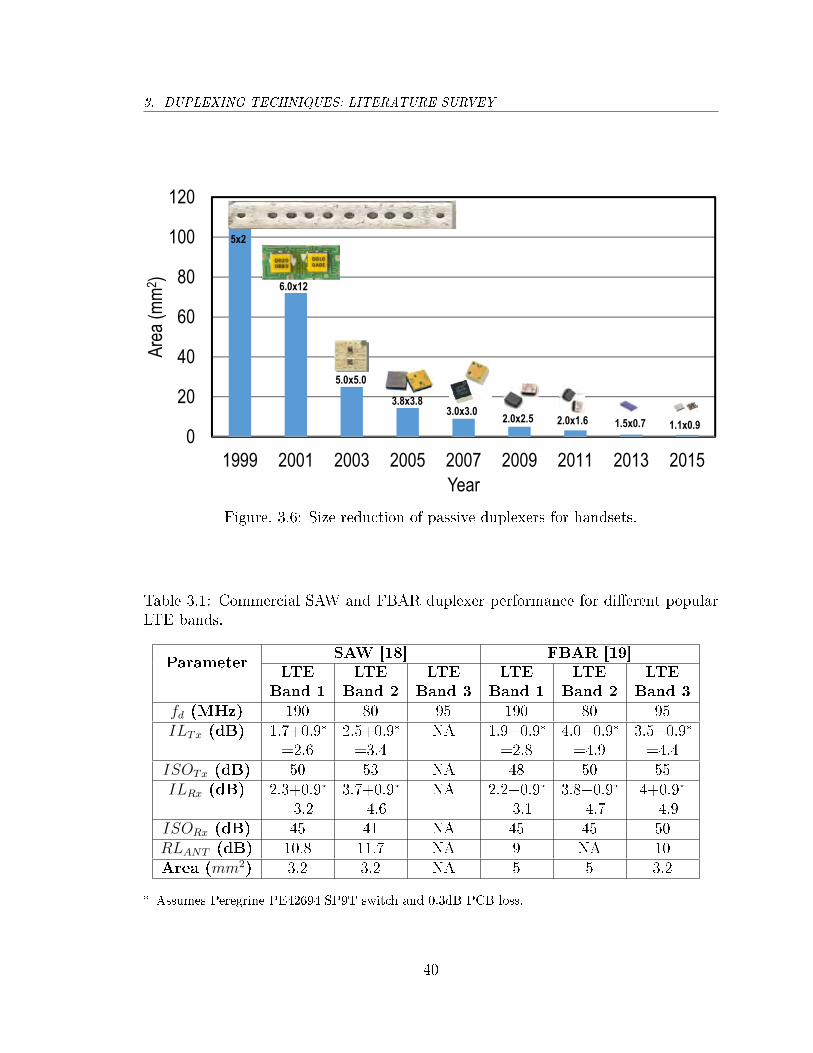
3. DUPLEXING TECHNIQUES: LITERATURE SURVEY
0
20
40
60
80
100
120
1999 2001 2003 2005 2007 2009 2011 2013 2015
Are
a (m
m2 )
Year
5x2
6.0x12
5.0x5.0
3.8x3.83.0x3.0
2.0x2.5 2.0x1.6 1.5x0.7 1.1x0.9
Figure. 3.6: Size reduction of passive duplexers for handsets.
Table 3.1: Commercial SAW and FBAR duplexer performance for dierent popularLTE bands.
ParameterSAW [18] FBAR [19]
LTEBand 1
LTEBand 2
LTEBand 3
LTEBand 1
LTEBand 2
LTEBand 3
fd (MHz) 190 80 95 190 80 95ILTx (dB) 1.7+0.9*
=2.62.5+0.9*
=3.4NA 1.9+0.9*
=2.84.0+0.9*
=4.93.5+0.9*
=4.4ISOTx (dB) 50 53 NA 48 50 55ILRx (dB) 2.3+0.9*
=3.23.7+0.9*
=4.6NA 2.2+0.9*
=3.13.8+0.9*
=4.74+0.9*
=4.9ISORx (dB) 45 41 NA 45 45 50RLANT (dB) 10.8 11.7 NA 9 NA 10Area (mm2) 3.2 3.2 NA 5 5 3.2
* Assumes Peregrine PE42694 SP9T switch and 0.3dB PCB loss.
40

3. DUPLEXING TECHNIQUES: LITERATURE SURVEY
3.2.2 Dual Antenna Scheme
The isolation between two antennas is important in mitigating self-interference. A
dual antenna approach is proposed in [20, 21] for full-duplex communication where
only cancellation at one frequency is required. Chen et al. [20] propose a decoupling
technique for enhancing the isolation between two closely spaced antennas. The tech-
nique contains two transmission lines and a shunt reactive component connected to
an impedance matching network at each port as shown in Fig.3.7a. Two miniaturised
monopole antennas (see Fig.3.7b) have been fabricated and an isolation of more than
20dB between the two antennas has been reported. However, the bandwidth is nar-
row. Larger spacing increases bandwidth and real-estate.
ANT.1
Z0, ø
ANT.2
jB
Matching
Network
Matching
Network
t1
t2
t3
t4
[SA]
[SA`
]
[SB]
[S]
Decoupling
Network
Port 1 Port 2
(a) (b)
Figure. 3.7: Decoupling technique for two antennas (a) function blocks (b) two closelyspaced miniaturised monopole antennas [20].
Kenworthy [21] presents a slightly dierent technique to improve the isolation
between two antennas. A dual antenna scheme (Tx and Rx) combined with an ana-
logue canceller and an adaptive digital baseband lter is utilised as illustrated in
41
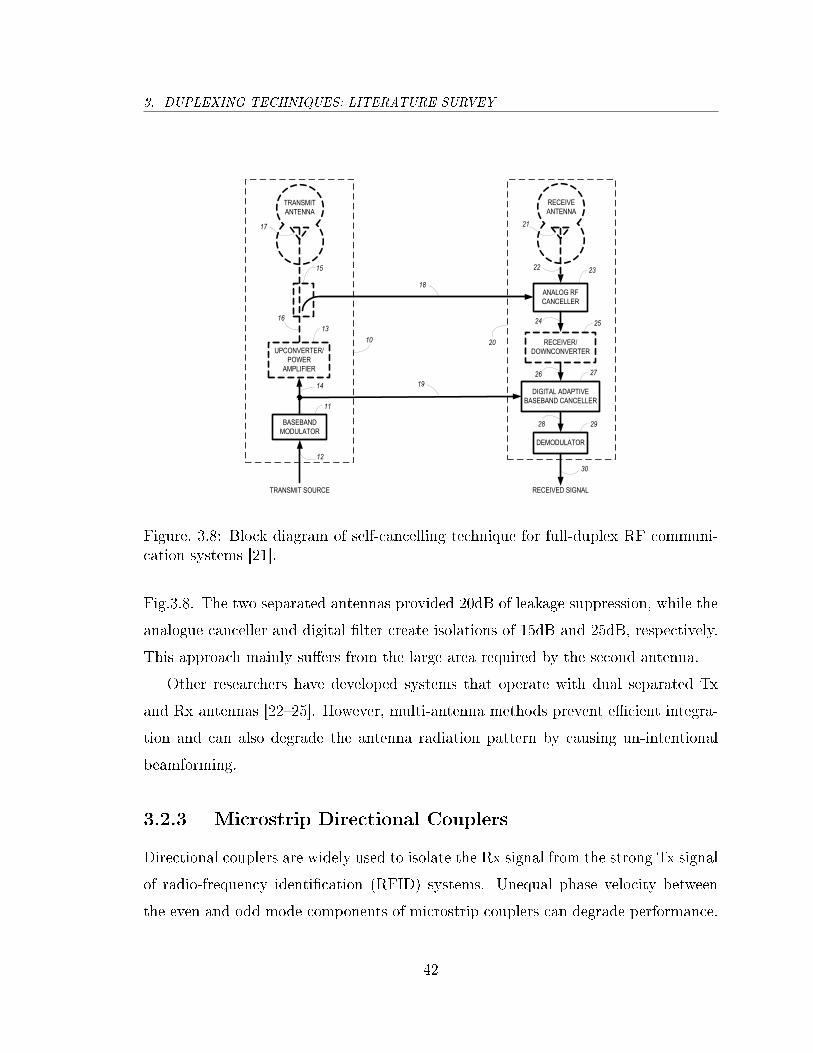
3. DUPLEXING TECHNIQUES: LITERATURE SURVEY
UPCONVERTER/
POWER
AMPLIFIER
BASEBAND
MODULATOR
TRANSMIT
ANTENNA
RECEIVER/
DOWNCONVERTER
DEMODULATOR
RECEIVE
ANTENNA
ANALOG RF
CANCELLER
DIGITAL ADAPTIVE
BASEBAND CANCELLER
RECEIVED SIGNALTRANSMIT SOURCE
12
11
13
10
16
15
17
14
18
19
21
20
22 23
24 25
26 27
28 29
30
Figure. 3.8: Block diagram of self-cancelling technique for full-duplex RF communi-cation systems [21].
Fig.3.8. The two separated antennas provided 20dB of leakage suppression, while the
analogue canceller and digital lter create isolations of 15dB and 25dB, respectively.
This approach mainly suers from the large area required by the second antenna.
Other researchers have developed systems that operate with dual separated Tx
and Rx antennas [2225]. However, multi-antenna methods prevent ecient integra-
tion and can also degrade the antenna radiation pattern by causing un-intentional
beamforming.
3.2.3 Microstrip Directional Couplers
Directional couplers are widely used to isolate the Rx signal from the strong Tx signal
of radio-frequency identication (RFID) systems. Unequal phase velocity between
the even and odd mode components of microstrip couplers can degrade performance.
42
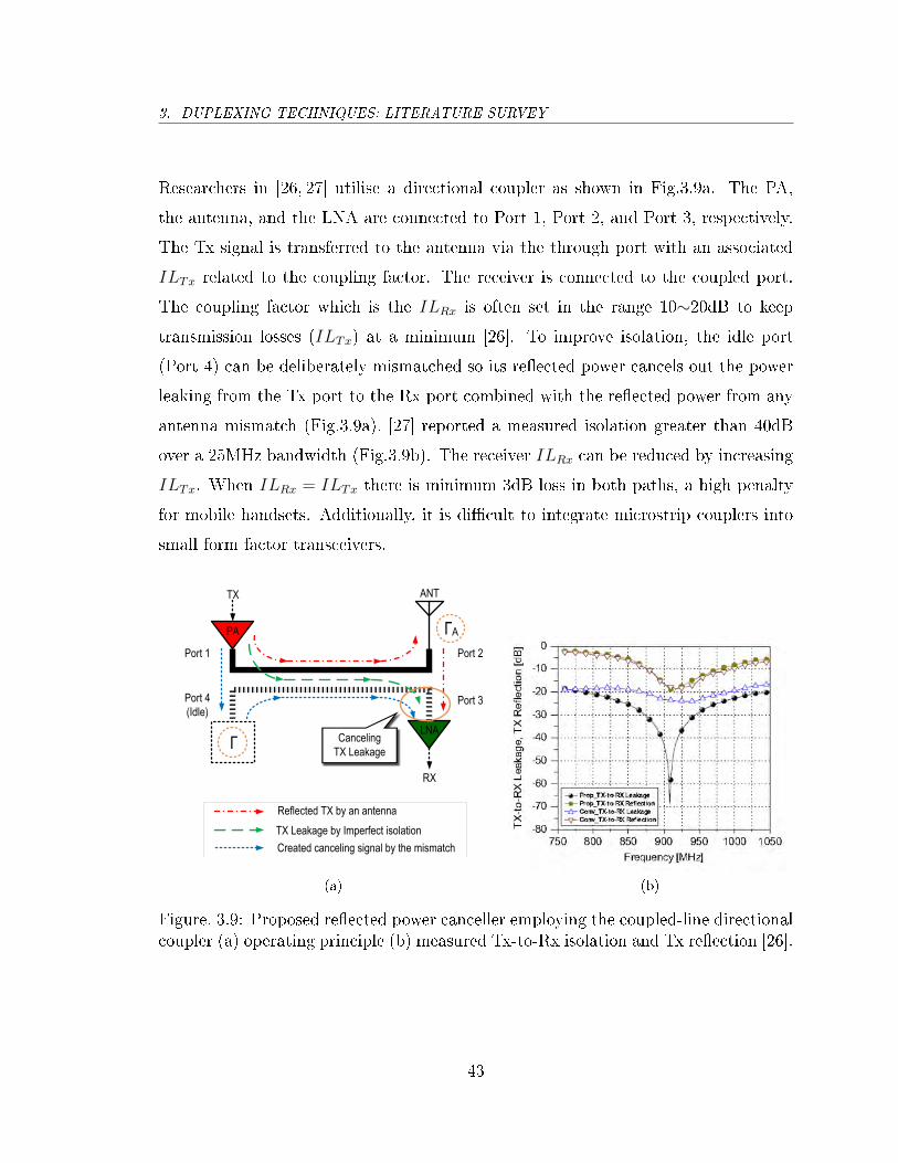
3. DUPLEXING TECHNIQUES: LITERATURE SURVEY
Researchers in [26, 27] utilise a directional coupler as shown in Fig.3.9a. The PA,
the antenna, and the LNA are connected to Port 1, Port 2, and Port 3, respectively.
The Tx signal is transferred to the antenna via the through port with an associated
ILTx related to the coupling factor. The receiver is connected to the coupled port.
The coupling factor which is the ILRx is often set in the range 10∼20dB to keep
transmission losses (ILTx) at a minimum [26]. To improve isolation, the idle port
(Port 4) can be deliberately mismatched so its reected power cancels out the power
leaking from the Tx port to the Rx port combined with the reected power from any
antenna mismatch (Fig.3.9a). [27] reported a measured isolation greater than 40dB
over a 25MHz bandwidth (Fig.3.9b). The receiver ILRx can be reduced by increasing
ILTx. When ILRx = ILTx there is minimum 3dB loss in both paths, a high penalty
for mobile handsets. Additionally, it is dicult to integrate microstrip couplers into
small form factor transceivers.
TX ANT
RX
PA
LNA
Port 1 Port 2
Port 3Port 4
(Idle)
Γ
ΓA
Canceling
TX Leakage
Reflected TX by an antenna
TX Leakage by Imperfect isolation
Created canceling signal by the mismatch
(a) (b)
Figure. 3.9: Proposed reected power canceller employing the coupled-line directionalcoupler (a) operating principle (b) measured Tx-to-Rx isolation and Tx reection [26].
43
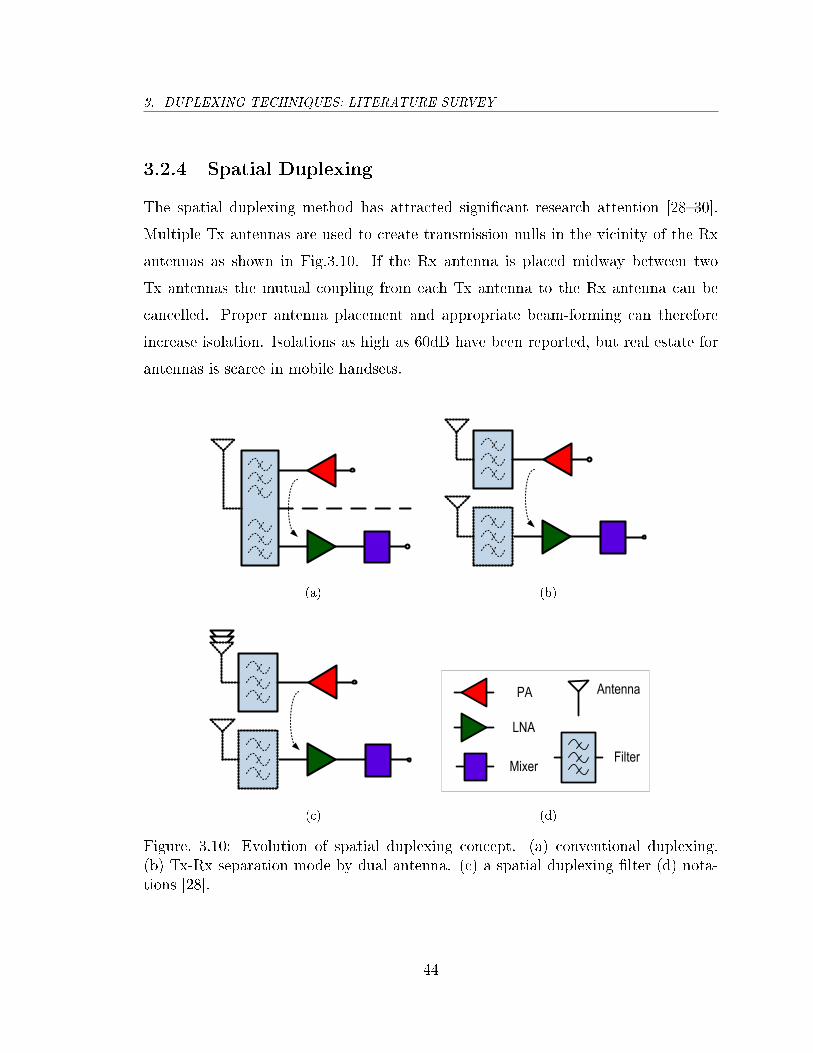
3. DUPLEXING TECHNIQUES: LITERATURE SURVEY
3.2.4 Spatial Duplexing
The spatial duplexing method has attracted signicant research attention [2830].
Multiple Tx antennas are used to create transmission nulls in the vicinity of the Rx
antennas as shown in Fig.3.10. If the Rx antenna is placed midway between two
Tx antennas the mutual coupling from each Tx antenna to the Rx antenna can be
cancelled. Proper antenna placement and appropriate beam-forming can therefore
increase isolation. Isolations as high as 60dB have been reported, but real estate for
antennas is scarce in mobile handsets.
(a) (b)
(c)
PA
LNA
Antenna
MixerFilter
(d)
Figure. 3.10: Evolution of spatial duplexing concept. (a) conventional duplexing.(b) Tx-Rx separation mode by dual antenna. (c) a spatial duplexing lter (d) nota-tions [28].
44

3. DUPLEXING TECHNIQUES: LITERATURE SURVEY
3.2.5 CMOS and Lumped Component Solutions
A bi-directional distributed amplier (DA) is a potential solution for single chip
Tx/Rx implementation. Leisten et al. [31] proposed the rst duplexer/circulator
structure using the versatile distributed amplier. This structure was non-tunable.
An electronically tunable active duplexer using DAs is shown in Fig.3.11 [32]. The
Tx/Rx DA module consisted of MESFET transistors [33], fabricated in a monolithic
microwave integrated circuit (MMIC). For mobile applications, the technique has
issues of noise, distortion and cost.
To Antenna or Termination
To Antenna or Termination
DA CELL
TPSN T
R
DA CELL
TPSNT
R
Tunable Active DuplexerTo Receiver
From Transmitter1
23
4
Figure. 3.11: Tx/Rx module schematic [31].
El.khatib et al. [34] proposed a CMOS based bi-directional DA as a tunable du-
plexer. This architecture achieves -26dB isolation and 10dB gain improvement by
using an on-chip dierential loop antenna, which is usually used at frequencies more
than 6GHz. This circuit is impractical at UMTS frequencies and also the duplexing
curve was not reported.
A lter based design employing bond wire inductors was proposed by Khatri
et al. [35]. The architecture included a dierential LNA with an integrated on-chip
passive lter to suppress the transmitter leakage in which the receiver signal is present.
To reduce packaging parasitics and chip area, a dierential conguration for the lter
was used as shown in Fig.3.12. In this structure the coupling capacitors are smaller
than the shunt capacitors. By using mode analysis [36], the mutual coupling eect
on lter response was considered. The results showed that closely placed bond wires
45

3. DUPLEXING TECHNIQUES: LITERATURE SURVEY
have a non-negligible mutual coupling eect, and as a result the ISOTx was only
10dB. The proposed circuit has been fabricated in 0.18µm CMOS technology and
C0
C0
C0
C0
0.5Ca 0.5Cb 0.5Cc
Vinp
Vinm
Voutp
Voutm
LBW LBW LBW
Figure. 3.12: Dierential lter with equal value bond wires as inductor replace-ments [35].
occupies 615µm2 chip area. The circuit has only a transmitter leakage suppression
of 10dB at 1920MHz and achieves a gain of 9.5dB at 2110MHz. However, the input
and output return losses are less than -13dB. Higher performance can be attained at
the expense of a higher noise gure and additional area for the lter itself.
The ninety-year-old hybrid transformer (HT) used to isolate the GO and RE-
TURN paths on a wired telephone line was recently implemented at RF [3740].
As presented in Fig.3.13a, the rst tunable integrated electrical balanced duplexer
(EBD) in CMOS technology is based on the hybrid autotransformer. The balance
network is tuned to the same impedance as the antenna at both Tx and Rx fre-
quencies, therefore, half of the Tx and Rx powers are dissipated in this network. The
implemented solution achieved an acceptable isolation of 50dB, although the insertion
loss of the Tx and Rx paths (4.2dB) would not attain the required UMTS duplexer
requirement. To address narrowband isolation and high insertion loss issues, a new
structure co-integrated with a noise matched LNA was proposed as per Fig.3.13b.
Isolation of 55dB over a 250MHz bandwidth and an insertion loss of 2.5dB were mea-
sured. Fig.3.13c presents a dierential implementation to address the common-mode
46

3. DUPLEXING TECHNIQUES: LITERATURE SURVEY
Tx-Rx rejection issue at the receiver port of the previous architecture. A peak isola-
tion of -70dB was measured over a bandwidth of 190MHz at a frequency of 1950MHz.
PA
LN
A
(a)
LN
AP
A
(b)
PA
Balun
PA
LNA
(c)
Figure. 3.13: Integrated electrical balance duplexers using (a) hybrid autotrans-former [38] (b) hybrid transformer [39] (c) dierential transformers [40].
47
3. DUPLEXING TECHNIQUES: LITERATURE SURVEY
In the previously discussed EBDs, the balancing load dissipates half the power
and needs to be adjusted to within 0.3% of the antenna impedance to meet the 50dB
isolation requirement; a very tough ask for the dynamically changing environment of
a mobile handset. However, the scheme does have a wide bandwidth and could be
useful in providing the rst 20dB of a two-stage isolation process.
3.3 Adaptive Duplexing Methods
3.3.1 Reducing Isolation Requirements
Improving transceiver performance can reduce the Tx noise and Rx tolerance to jam-
mers and therefore reduce the duplexer isolation requirements [41]. A feed-forward
loop around the PA can cancel the receive band noise [42]. The key problem is
eliminating the large Tx signal from the loop, without introducing more o-chip l-
ters [43]. Similarly, frequency translational feed-forward and feedback loops around
the receiver LNA can be used to remove strong blocking signals [44, 45]. Feedback
has stability and bandwidth issues while feed-forward has phase mismatching and LO
leak problems, but is still a viable option.
3.3.2 Cancelling Loops
Since the transmitter is the original source of the unwanted transmit signal and de-
sensitising noise signal, it should be possible to isolate these signals at the transmitter
and feed them into the receiver input appropriately scaled to cancel the Tx leakage.
In this way the Duplexer isolation requirements can be relaxed. A number of related
schemes have been reported.
Among them, a controlled amount of transmitter signal is bled into the receiver in
anti-phase to cancel the unwanted transmitter leakage [4648]. An integrated cancel-
lation system with an analogue control loop was demonstrated in [46] as illustrated in
Fig.3.14. The cancellation is applied at the LNA output to lower noise degradation
48
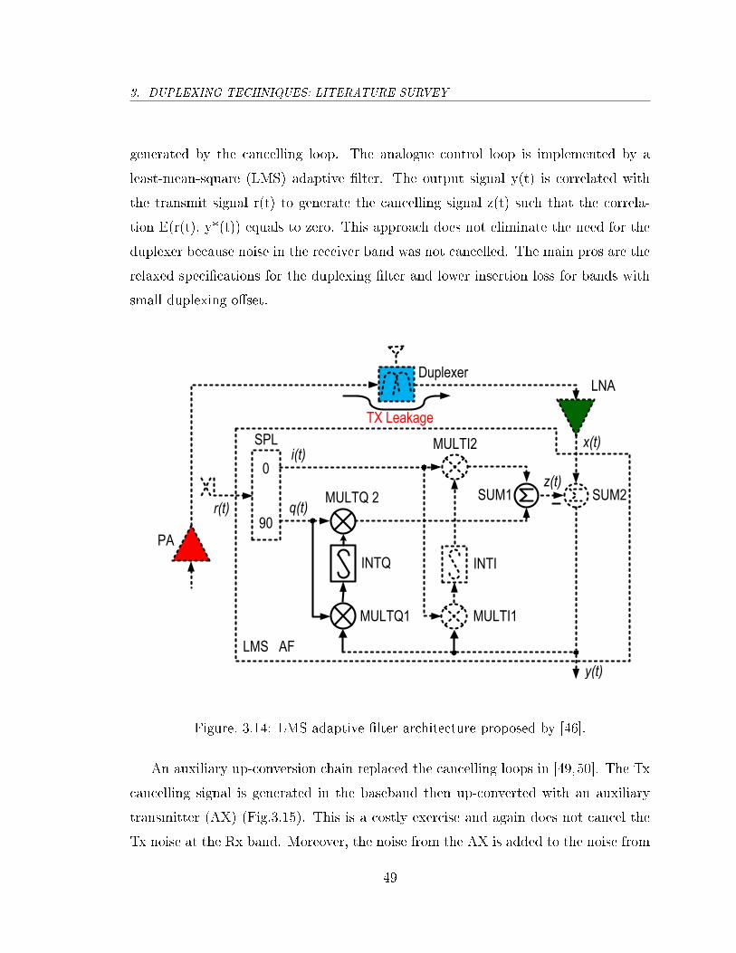
3. DUPLEXING TECHNIQUES: LITERATURE SURVEY
generated by the cancelling loop. The analogue control loop is implemented by a
least-mean-square (LMS) adaptive lter. The output signal y(t) is correlated with
the transmit signal r(t) to generate the cancelling signal z(t) such that the correla-
tion E(r(t), y*(t)) equals to zero. This approach does not eliminate the need for the
duplexer because noise in the receiver band was not cancelled. The main pros are the
relaxed specications for the duplexing lter and lower insertion loss for bands with
small duplexing oset.
Duplexer
SPL
PA
TX Leakage
MULTI2
MULTI1MULTQ1
MULTQ 2
INTQ INTI
SUM1 SUM2
LNA
0
90
LMS AF
r(t)
i(t)x(t)
q(t)
y(t)
z(t)
Figure. 3.14: LMS adaptive lter architecture proposed by [46].
An auxiliary up-conversion chain replaced the cancelling loops in [49,50]. The Tx
cancelling signal is generated in the baseband then up-converted with an auxiliary
transmitter (AX) (Fig.3.15). This is a costly exercise and again does not cancel the
Tx noise at the Rx band. Moreover, the noise from the AX is added to the noise from
49
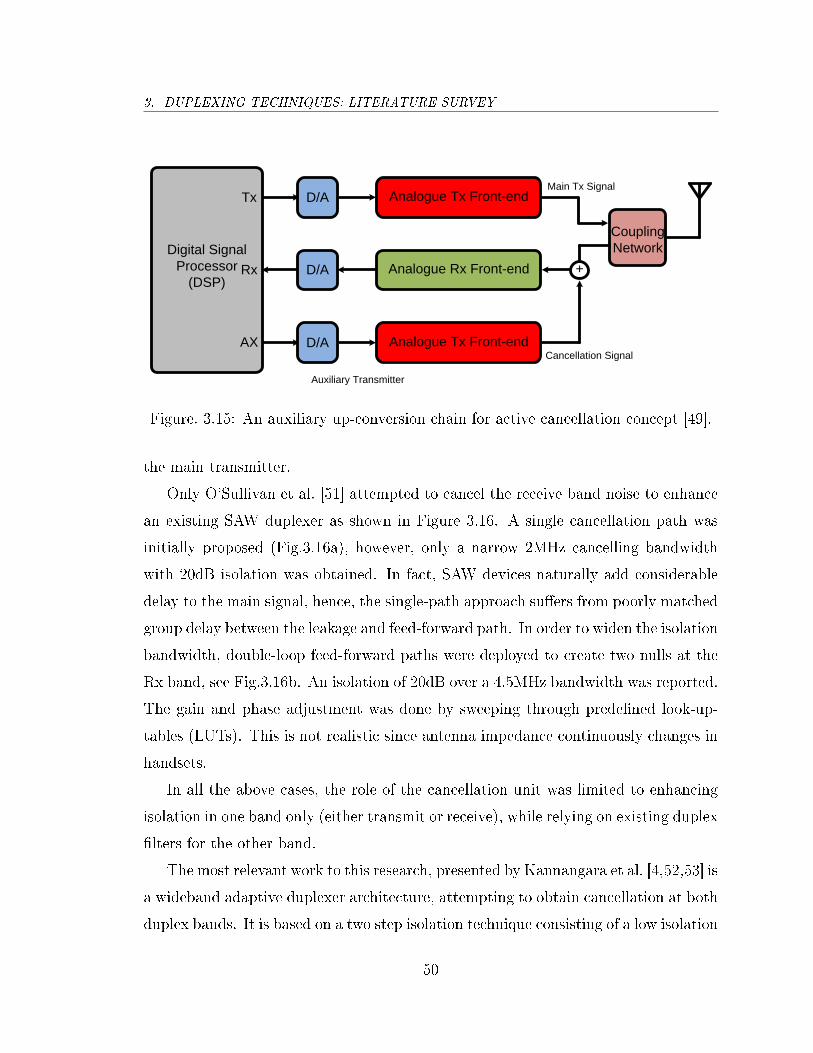
3. DUPLEXING TECHNIQUES: LITERATURE SURVEY
Digital Signal
Processor
(DSP)
Tx
Rx
AX
D/A Analogue Tx Front-end
D/A Analogue Rx Front-end
D/A Analogue Tx Front-end
Coupling
Network
+
Main Tx Signal
Cancellation Signal
Auxiliary Transmitter
Figure. 3.15: An auxiliary up-conversion chain for active cancellation concept [49].
the main transmitter.
Only O'Sullivan et al. [51] attempted to cancel the receive band noise to enhance
an existing SAW duplexer as shown in Figure 3.16. A single cancellation path was
initially proposed (Fig.3.16a), however, only a narrow 2MHz cancelling bandwidth
with 20dB isolation was obtained. In fact, SAW devices naturally add considerable
delay to the main signal, hence, the single-path approach suers from poorly matched
group delay between the leakage and feed-forward path. In order to widen the isolation
bandwidth, double-loop feed-forward paths were deployed to create two nulls at the
Rx band, see Fig.3.16b. An isolation of 20dB over a 4.5MHz bandwidth was reported.
The gain and phase adjustment was done by sweeping through predened look-up-
tables (LUTs). This is not realistic since antenna impedance continuously changes in
handsets.
In all the above cases, the role of the cancellation unit was limited to enhancing
isolation in one band only (either transmit or receive), while relying on existing duplex
lters for the other band.
The most relevant work to this research, presented by Kannangara et al. [4,52,53] is
a wideband adaptive duplexer architecture, attempting to obtain cancellation at both
duplex bands. It is based on a two step isolation technique consisting of a low isolation
50

3. DUPLEXING TECHNIQUES: LITERATURE SURVEY
EPCOS B4224
3rd Order
Notch Filter
Class A
Amplifier
BST
Phase Shifter
Variable
Attenuator
(a) (b)
EPCOS B4224
3rd Order
Notch Filter
Class A
Amplifier
BST
Phase Shifter
Variable
Attenuator
Class A
Amplifier
BST
Phase Shifter
Variable
Attenuator
(c) (d)
Figure. 3.16: Block diagram for the adaptive duplexer (a) single-path feed-forwardoperation. (b) dual-path feed-forward operation [51].
device (LID) providing approximately 20dB of initial isolation, followed by cancelling
loops providing the extra 30dB. Fig.3.17a shows the proposed conguration. A passive
wideband circulator is used as the LID. As discussed in Section 3.2, other alternatives
for the LID are separate antennas, directional couplers, and low selectivity strip-line
lters. All these devices cannot be integrated on a single chip. For further isolation,
two adaptive feed-forward cancellation loops control the amount of out-of-phase signal
needed to null out the remnants of the transmitter signal leaking through the LID.
The circuit has two degrees of freedom which enables the formation of two nulls
corresponding to the transmit and receive frequencies. The transmit signal, a low-
level pilot signal, and an adaptive algorithm are used to control the cancellation loop
51

3. DUPLEXING TECHNIQUES: LITERATURE SURVEY
Control Algonthm
Cist Function = E
Direct
Conversion
ReceiverTx
Pilot
Signal
RF Directional
CouplerRF Combiner
e1
e2
h1
h2A
Tx Leakage Signals
Rx SignalsTx Signals
Low Isolation
Device
Antenna
τa
τb
τc
(a)
(b)
Figure. 3.17: Adaptive duplexer (a) a dual-path feed-forward architecture. (b) thespectrum of the received signal [52].
nulls. A basic test bed showed 66dB of cancellation (including the 20dB circulator) in
the transmit band and 37dB in the receive band (Fig.3.17b); adequate for a CDMA
52
3. DUPLEXING TECHNIQUES: LITERATURE SURVEY
system [4]. The wideband circulator is only suitable for the base station when the
antenna is matched. However, this would not be suitable for handheld devices due to
the undetermined impedance of the antenna. A solution to the handheld problem is
the focus of this Thesis.
3.4 Summary
Passive and adaptive duplexing techniques are discussed in this chapter. Passive
duplexing methods include SAW and FBAR lters, dual antenna schemes, microstrip
directional couplers, spatial duplexing, and duplexers manufactured using CMOS and
lumped component technology. Electrical balancing duplexers are also reviewed in the
latter. Adaptive duplexing architectures are mainly based on two methods: reducing
the isolation requirements of transceiver and employing the cancelling loops. Both
methods use various feed forward techniques implemented in analogue and digital
domains, and with auxiliary transmitters.
The most relevant literature [4], presents active cancellation techniques for both
Tx leakage signals and Tx noise signals in the receiver, as is discussed in Section
3.3.2. Unfortunately, the proposed architecture cannot be integrated since the passive
circulator requires matched ports and is physically large in its wideband form. The
major aim of this research is to replace this bulky low isolation device (LID) by
tunable duplexing lters as discussed in the next chapter.
53

Chapter 4
Tunable Duplex Filter Design:
Theory
Mobile phones must support multiple frequency bands, requiring the handset industry
to include a set of RF switches and duplexers for each FDD frequency band, resulting
in substantial cost. With the growing number of frequency bands, the lack of a tunable
duplexer architecture is prominent. In the previous chapter, the two null adaptive
duplexing architecture uses a low isolation device (LID) to provide ≈20dB of initial
isolation over the target frequency range. The initial isolation is required to reduce
the signal level in the cancelling loops and minimise the insertion loss of the coupler
and combiner (Fig.3.17). As such it should be at least 10dB and preferably above
20dB. As mentioned, the LID is usually implemented using a circulator, a directional
coupler, or an L-C duplex lter. The latter could potentially be integrated on-chip. In
this chapter, the theory of such a lter is presented. It uses two dierent combinations
of notch lters which resonate at the Tx and the Rx frequencies. Tuning and losses
are key parameters to be addressed. RLC resonance theory is briey discussed in
Section 4.1. Two bandpass-bandstop lter topologies are analysed in Section 4.2, and
nally a summary is given in Section 4.3.
54
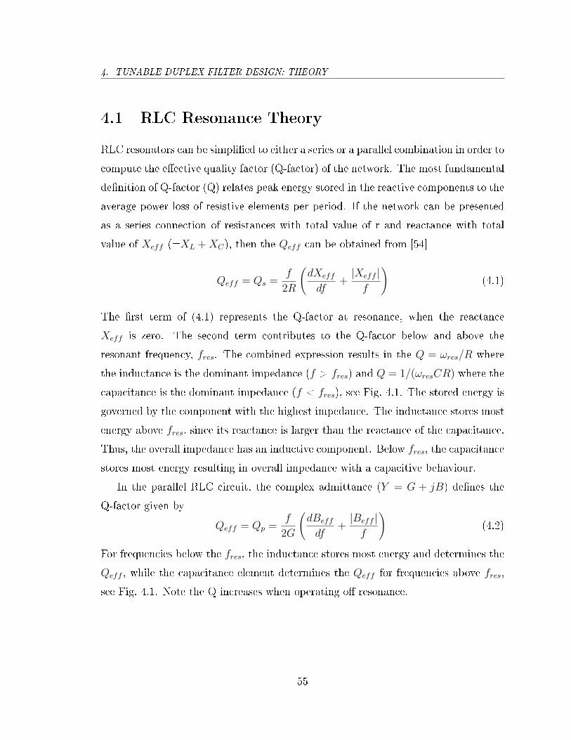
4. TUNABLE DUPLEX FILTER DESIGN: THEORY
4.1 RLC Resonance Theory
RLC resonators can be simplied to either a series or a parallel combination in order to
compute the eective quality factor (Q-factor) of the network. The most fundamental
denition of Q-factor (Q) relates peak energy stored in the reactive components to the
average power loss of resistive elements per period. If the network can be presented
as a series connection of resistances with total value of r and reactance with total
value of Xeff (=XL +XC), then the Qeff can be obtained from [54]
Qeff = Qs =f
2R
(dXeff
df+|Xeff |f
)(4.1)
The rst term of (4.1) represents the Q-factor at resonance, when the reactance
Xeff is zero. The second term contributes to the Q-factor below and above the
resonant frequency, fres. The combined expression results in the Q = ωres/R where
the inductance is the dominant impedance (f > fres) and Q = 1/(ωresCR) where the
capacitance is the dominant impedance (f < fres), see Fig. 4.1. The stored energy is
governed by the component with the highest impedance. The inductance stores most
energy above fres, since its reactance is larger than the reactance of the capacitance.
Thus, the overall impedance has an inductive component. Below fres, the capacitance
stores most energy resulting in overall impedance with a capacitive behaviour.
In the parallel RLC circuit, the complex admittance (Y = G + jB) denes the
Q-factor given by
Qeff = Qp =f
2G
(dBeff
df+|Beff |f
)(4.2)
For frequencies below the fres, the inductance stores most energy and determines the
Qeff , while the capacitance element determines the Qeff for frequencies above fres,
see Fig. 4.1. Note the Q increases when operating o resonance.
55
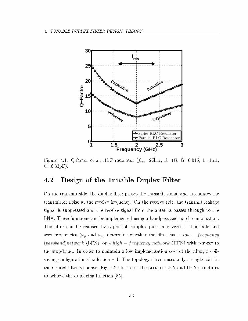
4. TUNABLE DUPLEX FILTER DESIGN: THEORY
1 1.5 2 2.5 30
5
10
15
20
25
30
Frequency (GHz)
Q−F
acto
r
Inductive
Capacitive Inductive
Capacitive
Series RLC ResonatorParallel RLC Resonator
fres
Figure. 4.1: Q-factor of an RLC resonator (fres=2GHz, R=1Ω, G=0.01S, L=1nH,C=6.33pF).
4.2 Design of the Tunable Duplex Filter
On the transmit side, the duplex lter passes the transmit signal and attenuates the
transmitter noise at the receive frequency. On the receive side, the transmit leakage
signal is suppressed and the receive signal from the antenna passes through to the
LNA. These functions can be implemented using a bandpass and notch combination.
The lter can be realised by a pair of complex poles and zeroes. The pole and
zero frequencies (ωp and ωz) determine whether the lter has a low − frequency
(passband)network (LFN), or a high − frequency network (HFN) with respect to
the stop-band. In order to maintain a low implementation cost of the lter, a coil-
saving conguration should be used. The topology chosen uses only a single coil for
the desired lter response. Fig. 4.2 illustrates the possible LFN and HFN structures
to achieve the duplexing function [55].
56
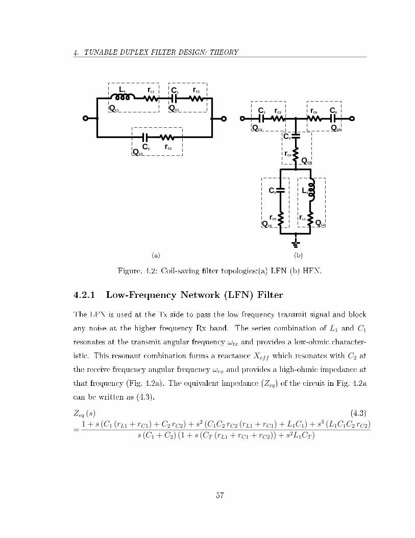
4. TUNABLE DUPLEX FILTER DESIGN: THEORY
L1 C1rL1 rC1
C2 rC2
QC2
QC1QL1
(a)
L2C5
C4
QC5
QC4
QL2
C3
QC3
C6
QC6
rC3 rC6
rC4
rL1rC5
(b)
Figure. 4.2: Coil-saving lter topologies:(a) LFN (b) HFN.
4.2.1 Low-Frequency Network (LFN) Filter
The LFN is used at the Tx side to pass the low frequency transmit signal and block
any noise at the higher frequency Rx band. The series combination of L1 and C1
resonates at the transmit angular frequency ωtx and provides a low-ohmic character-
istic. This resonant combination forms a reactance Xeff which resonates with C2 at
the receive frequency angular frequency ωrx and provides a high-ohmic impedance at
that frequency (Fig. 4.2a). The equivalent impedance (Zeq) of the circuit in Fig. 4.2a
can be written as (4.3).
(4.3)Zeq (s)
=1 + s (C1 (rL1 + rC1) + C2 rC2) + s2 (C1C2 rC2 (rL1 + rC1) + L1C1) + s3 (L1C1C2 rC2)
s (C1 + C2) (1 + s (CT (rL1 + rC1 + rC2)) + s2L1CT )
57

4. TUNABLE DUPLEX FILTER DESIGN: THEORY
For simplicity, we initially assume that the LFN network is perfectly lossless, i.e. all
the series resistances are equal to zero. As a result, the Zeq is simplied to (4.4).
Zeq (s) ' 1 + s2 (L1C1)
s (C1 + C2) (1 + s2L1CT )'
1 + s2
ω2z
s (C1 + C2)(
1 + s2
ω2p
) (4.4)
The latter expression has zero and pole complex pairs with angular frequencies
ωz '1√L1C1
ωp '1√L1CT
(4.5)
where CT = C1C2
C1+C2. If C1 << C2, the zero is directly adjacent to the pole creating a
steep transition region between them in the plot of Zeq. This is illustrated in Fig. 4.3
which plots |Zeq| of (4.3) versus frequency.
1.6 1.8 2 2.2 2.40
10
20
30
40
50
Frequency (GHz)
Imp
edan
ce M
agn
itu
de
(dB
Ω)
Figure. 4.3: Magnitude of Zeq vs frequency for 2% increments in the nominal valueof C1 (from the right). (Q = 100)
We now discuss the tuning and losses of the LFN network.
58
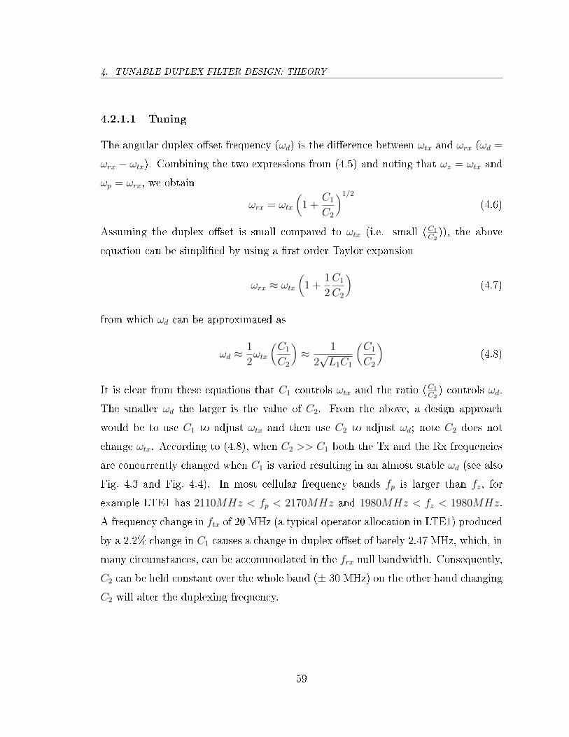
4. TUNABLE DUPLEX FILTER DESIGN: THEORY
4.2.1.1 Tuning
The angular duplex oset frequency (ωd) is the dierence between ωtx and ωrx (ωd =
ωrx − ωtx). Combining the two expressions from (4.5) and noting that ωz = ωtx and
ωp = ωrx, we obtain
ωrx = ωtx
(1 +
C1
C2
)1/2
(4.6)
Assuming the duplex oset is small compared to ωtx (i.e. small (C1
C2)), the above
equation can be simplied by using a rst order Taylor expansion
ωrx ≈ ωtx
(1 +
1
2
C1
C2
)(4.7)
from which ωd can be approximated as
ωd ≈1
2ωtx
(C1
C2
)≈ 1
2√L1C1
(C1
C2
)(4.8)
It is clear from these equations that C1 controls ωtx and the ratio (C1
C2) controls ωd.
The smaller ωd the larger is the value of C2. From the above, a design approach
would be to use C1 to adjust ωtx and then use C2 to adjust ωd; note C2 does not
change ωtx. According to (4.8), when C2 >> C1 both the Tx and the Rx frequencies
are concurrently changed when C1 is varied resulting in an almost stable ωd (see also
Fig. 4.3 and Fig. 4.4). In most cellular frequency bands fp is larger than fz, for
example LTE1 has 2110MHz < fp < 2170MHz and 1980MHz < fz < 1980MHz.
A frequency change in ftx of 20 MHz (a typical operator allocation in LTE1) produced
by a 2.2% change in C1 causes a change in duplex oset of barely 2.47 MHz, which, in
many circumstances, can be accommodated in the frx null bandwidth. Consequently,
C2 can be held constant over the whole band (± 30 MHz) on the other hand changing
C2 will alter the duplexing frequency.
59
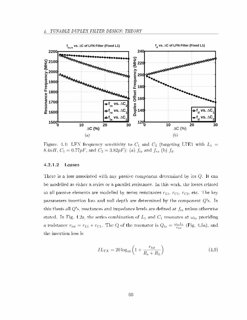
4. TUNABLE DUPLEX FILTER DESIGN: THEORY
0 10 20 301500
1600
1700
1800
1900
2000
2100
2200
ftx,rx
vs. ΔC of LFN Filter (Fixed L1)
ΔC (%)
Res
on
ance
Fre
qu
ency
(M
Hz)
frx
vs. ΔC2
frx
vs. ΔC1
ftx
vs. ΔC1
(a)
0 10 20 30120
140
160
180
200
220
240
fd vs. ΔC of LFN Filter (Fixed L1)
ΔC (%)
Du
ple
x O
ffse
t F
req
uen
cy (
MH
z)
fd vs. ΔC
1
fd vs. ΔC
2
(b)
Figure. 4.4: LFN frequency sensitivity to C1 and C2 (targeting LTE1 with L1 =8.4nH, C1 = 0.77pF , and C2 = 3.82pF ): (a) ftx and frx (b) fd.
4.2.1.2 Losses
There is a loss associated with any passive component determined by its Q. It can
be modelled as either a series or a parallel resistance. In this work, the losses related
to all passive elements are modelled by series resistances rL1, rC1, rC2, etc. The key
parameters insertion loss and null depth are determined by the component Q's. In
this thesis all Q's, reactances and impedance levels are dened at ftx unless otherwise
stated. In Fig. 4.2a, the series combination of L1 and C1 resonates at ωtx providing
a resistance rtot = rL1 + rC1. The Q of the resonator is Qtx = ωtxL1
rtot(Fig. 4.5a), and
the insertion loss is
ILTX = 20 log10
(1 +
rtotRs +RL
)(4.9)
60
4. TUNABLE DUPLEX FILTER DESIGN: THEORY
L1 C1
rL1 rC1
(a)
C2 p
Reff p
RC2 p
Xeff p
(b)
Figure. 4.5: LFN equivalent circuit resonating at: (a) ftx (b) frx.
When source and load resistances are equal (RS = RL), the insertion loss becomes
ILTX = 20 log10
1 +
(XL1
RL
)/QL1 +
(XC1
RL
)/QC1
2
(4.10)
At ωrx, which is above ωtx, the resonant combination L1,C1 provides an eective
reactance Xeff with an associated Qeff .
Xeff = ωrxL1 −1
ωrxC1
= ωrx
(L1C1ω
2rx − 1
C1ω2rx
)
Qeff =ωrx
rtot
(L1C1ω
2rx − 1
C1ω2rx
)(4.11)
Converting to a parallel circuit representation better suited to the evaluation of the
parallel resonance at ωrx yields
Xeff p = Xeff
(1 +Q2
eff
Q2eff
)
Reff p = Qeff Xeff (4.12)
61
4. TUNABLE DUPLEX FILTER DESIGN: THEORY
The eective parallel resistance is combined with the parallel resistance representation
of the lossy capacitor C2 (Fig. 4.5b), RC2 p = rC2(1 + Q2C2/(1 + ∆)2) where ∆ is the
fractional duplex frequency (∆ = fdftx) and the (1−∆)2 term converts QC2 (dened at
ftx) to frx. At ωrx, Xeff p resonates with C2 p giving a resistance between the ports
of Rtot. The null-depth becomes
ISORX = 20 log10
(1 +
Rtot
Rs +RL
)(4.13)
where 1Rtot
= 1Reff p
+ 1RC2 p
. Fig. 4.6a and Fig. 4.6b show the ILTX and ISORX for
dierent Q's of the inductance L1 and the capacitances C1 and C2. Component values
are the same as for Fig. 4.4. There is little to be gained by vastly increasing the Q
of one component over the other. The Q of C2 has little impact on the null-depth
indicating losses are heavily dependent on the primary resonant circuit (L1−C1). The
closer in frequency the null is to the passband, the lower the Qeff of the resonator;
setting ω2rx = 1/(L1C1) in (4.11) would result in Qeff equal to zero. There is also a
trade-o between null-depth and insertion loss. Choosing components with the higher
impedance (larger L and smaller C) will improve null-depth at the expense of insertion
loss. Fig. 4.6.c and Fig. 4.6.d show contours of ILTX and ISORX plotted against nor-
malised inductor impedance (XL
RL) for dierent Q; where all components have the same
Q. Note that the load impedance (RL) is not always 50Ω. The left hand plot is for
∆ of 10% and the right hand plot is for 5%. These two values cover most of the com-
mon LTE bands. The plots describe the trade-o between insertion loss and isolation.
For example, starting with the upper red curves, a specied null-depth (isolation) of
10dB with component Q's of 25 requires a normalised impedance of 8.5 (marked 1).
Using this value of normalised impedance and the lower blue curves (marked 2), the
resulting insertion loss of 2.7dB is obtained (marked 3). At the lower duplexing o-
set, the same Q and null-depth require a normalised impedance of 25 and results in
a somewhat degraded insertion loss of 6.0dB. Similarly, increasing the isolation to
20dB increases the impedance to 35 and the insertion loss to 7.9dB. Peak voltage
62
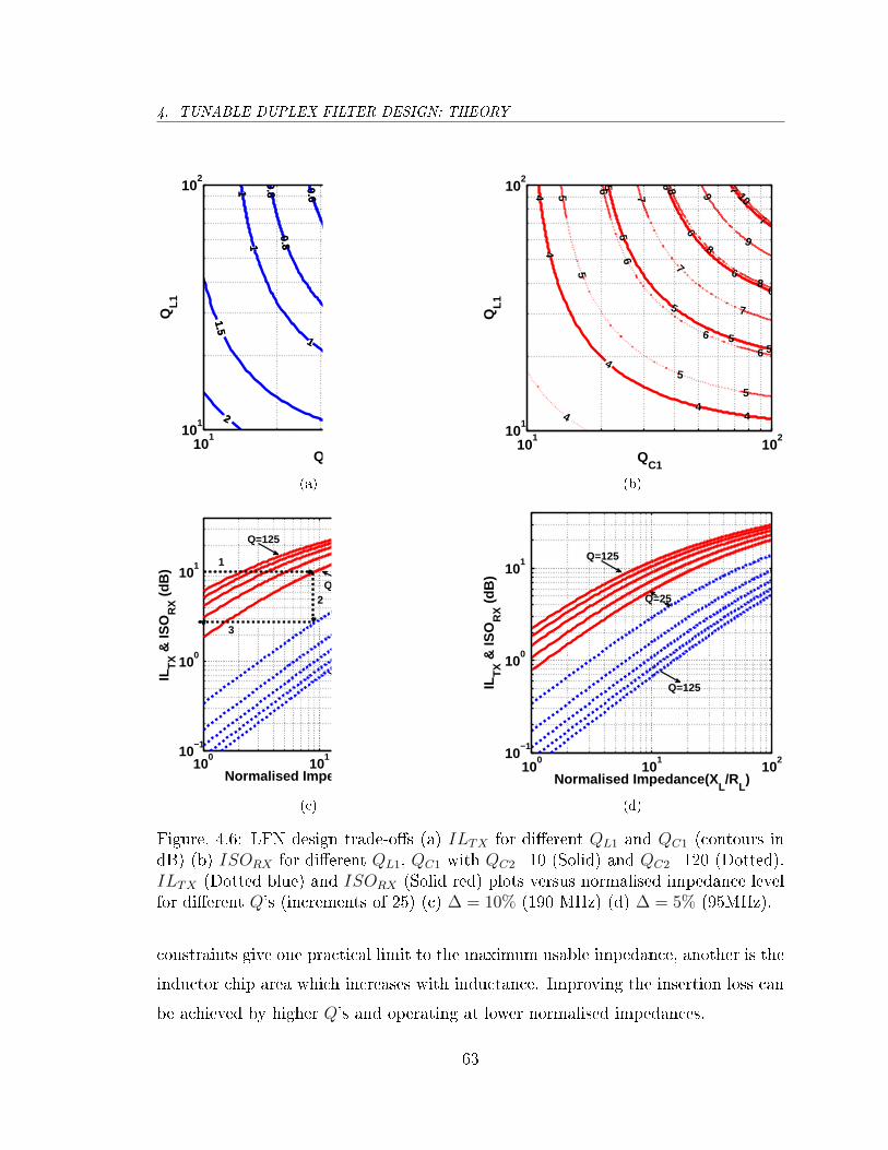
4. TUNABLE DUPLEX FILTER DESIGN: THEORY
0.4
0.4
0.4
0.6
0.6
0.6
0.6
0.80.8
0.8
0.80.8
11
1
11
1.5
1.5
2
QC1
QL
1
0.4
0.4
0.4
0.6
0.6
0.6
0.6
0.80.8
0.8
0.80.8
11
1
11
1.5
1.5
2
101
10210
1
102
(a)
44
4
44
55
5
55
6
6
6
6
7
7
QC1
QL
1
4
5
5
5
5
6
6
6
6
7
7
7
8
8
8
9
9
10
101
10210
1
102
(b)
100
101
10210
−1
100
101
ILT
X &
ISO
RX (
dB)
Normalised Impedance(XL/R
L)
Q=125
Q=125
Q=25
1
3
2
(c)
100
101
10210
−1
100
101
ILT
X &
ISO
RX (
dB)
Normalised Impedance(XL/R
L)
Q=25
Q=125
Q=125
(d)
Figure. 4.6: LFN design trade-os (a) ILTX for dierent QL1 and QC1 (contours indB) (b) ISORX for dierent QL1, QC1 with QC2=10 (Solid) and QC2=120 (Dotted).ILTX (Dotted blue) and ISORX (Solid red) plots versus normalised impedance levelfor dierent Q's (increments of 25) (c) ∆ = 10% (190 MHz) (d) ∆ = 5% (95MHz).
constraints give one practical limit to the maximum usable impedance, another is the
inductor chip area which increases with inductance. Improving the insertion loss can
be achieved by higher Q's and operating at lower normalised impedances.
63

4. TUNABLE DUPLEX FILTER DESIGN: THEORY
Table 4.1 summarises the ILTx versus ISORx trade-o. Typically the performance
at a Q of 25 is what might be hoped for in a fully integrated SOS solution which
benets from the improved inductors relative to bulk CMOS. Even so ILTx at 5dB
is a bit high at the minimum required 15dB isolation. In reality the all integrated
solution is limited to LTE band 1 (∆ = 10%). On the other hand, chip inductors now
have Q's above 100 and therefore a discrete solution would have insertion loss of less
than 0.5dB at the same isolation level. Even with a lower ∆ = 5% the insertion loss
is still a respectable 2.8dB.
Table 4.1: Summary of ILTx versus ISORx for three Q's in the LFN lter. (∆ = 10%)
ILTx (dB) ISORx=10dB ISORx=15dB ISORx=20dBQ=25 2.7 4.93 7.9Q=50 0.85 1.8 3.2Q=100 0.2 0.47 0.9
4.2.2 High-Frequency Network (HFN) Filter
The HFN network is on the receive side and blocks low frequency Tx and passes
the high frequency Rx signals. In Fig. 4.2b, the parallel combination of L2 and C5
resonates at ωrx providing a high-ohmic impedance. This resonant tank provides a
reactance Xeff that resonates with C4 at ωtx, resulting in a low impedance. For
simplicity, we initially assume that the HFN network is perfectly lossless and the
eects of C3 and C6 are also neglected. The zero and pole complex pairs are
ωz '1√L2CT
ωp '1√L2C5
(4.14)
where CT = C4 + C5. If C4 << C5, the pole is directly adjacent to the zero creating
a steep transition region in the plot of Zeq.
64

4. TUNABLE DUPLEX FILTER DESIGN: THEORY
4.2.2.1 Tuning
Setting ωz = ωtx and ωp = ωrx and assuming that the duplex oset is small compared
to ωtx (i.e. small (C4/C5)), ωd can be simplied similar to the LFN case
ωd ≈1
2ωrx
(C4
C5
)≈ 1
2√L2C5
(C4
C5
)(4.15)
It is clear that C5 controls ωrx and the ratio C4/C5 controls ωd. The smaller ωd the
smaller the value of C4. From the above, a design approach would be to use C5 to
adjust the notch to ωrx and then use C4 to adjust the passband. Fig. 4.7 shows that
when C4 << C5, a frequency change in frx of 20MHz produced by a 2% change in
C5 causes a change in duplex oset of 4.9MHz. Consequently, C4 can be adjusted to
compensate the fd change or held constant depending on the null bandwidth.
0 10 20 301600
1700
1800
1900
2000
2100
2200
ftx,rx
vs. ΔC of HFN Filter (Fixed L1)
ΔC (%)
Res
on
ance
Fre
qu
ency
(M
Hz)
frx
vs. ΔC5
ftx
vs. ΔC4
ftx
vs. ΔC5
(a)
0 10 20 30100
120
140
160
180
200
220
240
260
fd vs. ΔC of HFN Filter (Fixed L1)
ΔC (%)
Du
ple
x O
ffse
t F
req
uen
cy (
MH
z)
fd vs. ΔC
4
fd vs. ΔC
5
(b)
Figure. 4.7: HFN frequency sensitivity to C4 and C5 (targeting LTE1): (a) ftx andfrx (b) fd.
65
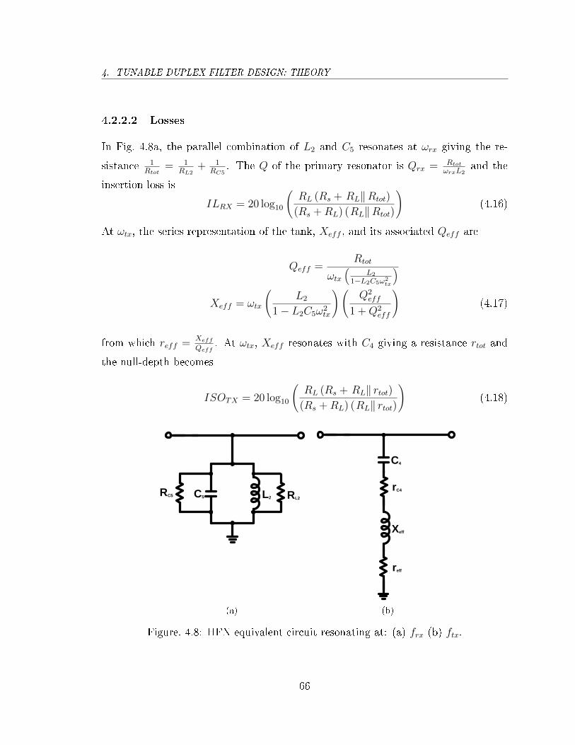
4. TUNABLE DUPLEX FILTER DESIGN: THEORY
4.2.2.2 Losses
In Fig. 4.8a, the parallel combination of L2 and C5 resonates at ωrx giving the re-
sistance 1Rtot
= 1RL2
+ 1RC5
. The Q of the primary resonator is Qrx = Rtot
ωrxL2and the
insertion loss is
ILRX = 20 log10
(RL (Rs + RL‖Rtot)
(Rs +RL) (RL‖Rtot)
)(4.16)
At ωtx, the series representation of the tank, Xeff , and its associated Qeff are
Qeff =Rtot
ωtx
(L2
1−L2C5ω2tx
)Xeff = ωtx
(L2
1− L2C5ω2tx
)(Q2
eff
1 +Q2eff
)(4.17)
from which reff =Xeff
Qeff. At ωtx, Xeff resonates with C4 giving a resistance rtot and
the null-depth becomes
ISOTX = 20 log10
(RL (Rs + RL‖ rtot)
(Rs +RL) (RL‖ rtot)
)(4.18)
L2C5RC5 RL2
(a)
Xeff
C4
reff
rC4
(b)
Figure. 4.8: HFN equivalent circuit resonating at: (a) frx (b) ftx.
66
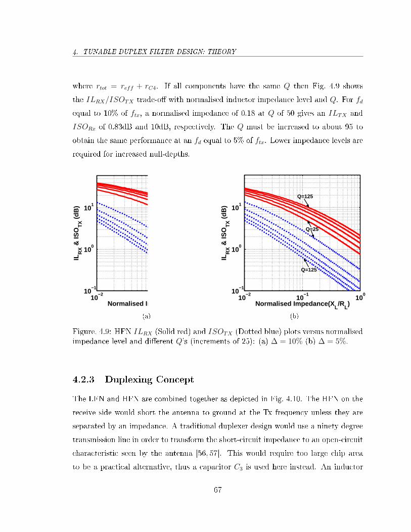
4. TUNABLE DUPLEX FILTER DESIGN: THEORY
where rtot = reff + rC4. If all components have the same Q then Fig. 4.9 shows
the ILRX/ISOTX trade-o with normalised inductor impedance level and Q. For fd
equal to 10% of ftx, a normalised impedance of 0.18 at Q of 50 gives an ILTX and
ISORx of 0.83dB and 10dB, respectively. The Q must be increased to about 95 to
obtain the same performance at an fd equal to 5% of ftx. Lower impedance levels are
required for increased null-depths.
10−2
10−1
10010
−1
100
101
ILR
X &
ISO
TX (
dB)
Normalised Impedance(XL/R
L)
Q=125
Q=125
Q=25
(a)
10−2
10−1
10010
−1
100
101
ILR
X &
ISO
TX (
dB)
Normalised Impedance(XL/R
L)
Q=125
Q=125
Q=25
(b)
Figure. 4.9: HFN ILRX (Solid red) and ISOTX (Dotted blue) plots versus normalisedimpedance level and dierent Q's (increments of 25): (a) ∆ = 10% (b) ∆ = 5%.
4.2.3 Duplexing Concept
The LFN and HFN are combined together as depicted in Fig. 4.10. The HFN on the
receive side would short the antenna to ground at the Tx frequency unless they are
separated by an impedance. A traditional duplexer design would use a ninety degree
transmission line in order to transform the short-circuit impedance to an open-circuit
characteristic seen by the antenna [56, 57]. This would require too large chip area
to be a practical alternative, thus a capacitor C3 is used here instead. An inductor
67

4. TUNABLE DUPLEX FILTER DESIGN: THEORY
C
L
CL
C
Tx (PA)
PORT 1
ANT
PORT 2
Rx (LNA)
PORT 3
1 1
2
3
2
C6
C4
C5
LANT
Figure. 4.10: Proposed tunable duplex lter conguration.
(Lant) resonates with C3 to present an open-circuit. Such an inductance can be
absorbed into an antenna-tuning unit (ATU), which is common in mobile phones.
These components introduce a penalty in ILRX of about 1.5dB. The capacitances C1
and C5 are adjusted to give channel-tuning range of 80MHz in eight steps using a
binary weighted digitally switched capacitor bank (DSCB). Resonance can produce
high voltages, which prevents the possibility of using varactor devices. A feasible
solution is to use a switched capacitor bank with a number of stacked transistors for
handling higher voltages. It is possible to estimate a worst-case voltage by assuming
lossless components. The LFN resonant circuit on the transmit side (L1-C1) must
pass a current equal to that passing through the load IL =√
PRL. The voltage across
C1 (VC1) has the same amplitude as that across L1, equal to ILXL1. This leads to
the following equation for VC1
log10
(VC1√RL
)= log10
(XL
RL
)+PdBm
20− 1.5 + log10
(√2)
(4.19)
68
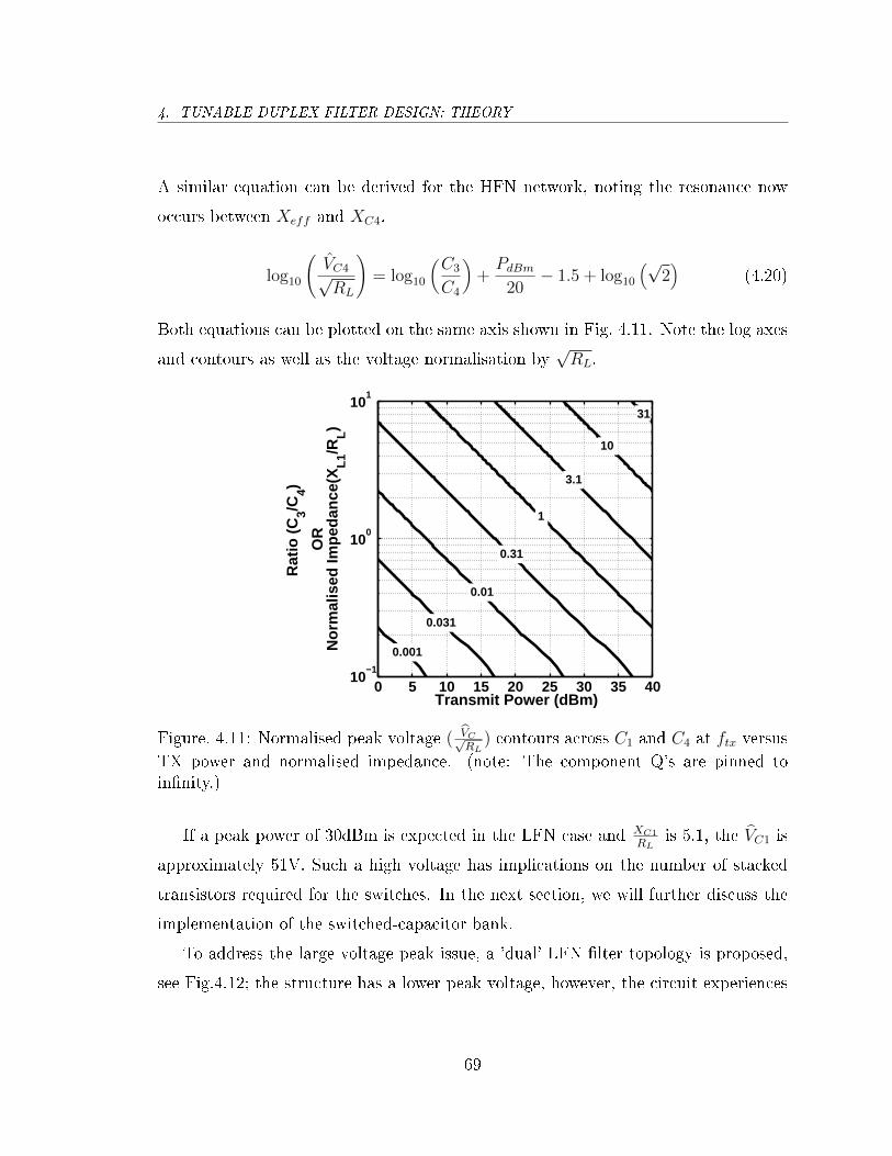
4. TUNABLE DUPLEX FILTER DESIGN: THEORY
A similar equation can be derived for the HFN network, noting the resonance now
occurs between Xeff and XC4,
log10
(VC4√RL
)= log10
(C3
C4
)+PdBm
20− 1.5 + log10
(√2)
(4.20)
Both equations can be plotted on the same axis shown in Fig. 4.11. Note the log axes
and contours as well as the voltage normalisation by√RL.
Transmit Power (dBm)
R
atio
(C
3/C4)
OR
Nor
mal
ised
Impe
danc
e(X
L1/R
L)
0 5 10 15 20 25 30 35 4010
−1
100
101
0.001
0.031
0.01
0.31
1
3.1
10
31
Figure. 4.11: Normalised peak voltage ( VC√RL
) contours across C1 and C4 at ftx versusTX power and normalised impedance. (note: The component Q's are pinned toinnity.)
If a peak power of 30dBm is expected in the LFN case and XC1
RLis 5.1, the VC1 is
approximately 51V. Such a high voltage has implications on the number of stacked
transistors required for the switches. In the next section, we will further discuss the
implementation of the switched-capacitor bank.
To address the large voltage peak issue, a 'dual' LFN lter topology is proposed,
see Fig.4.12; the structure has a lower peak voltage, however, the circuit experiences
69

4. TUNABLE DUPLEX FILTER DESIGN: THEORY
QC7
L3 rL3
C8 rC8
C7 rC7QL3
QC8
Figure. 4.12: Proposed coil-saving (dual) LFN lter topology.
a higher peak current at resonance. It is worthwhile to highlight that since the max-
imum voltage level is lower, less transistors are stacked in a switched capacitor unit,
increasing Q-factor. Assuming lossless components, the ftx and the frx, and con-
sequently fd vary with C7 and C8 as per Fig. 4.13a and Fig. 4.13b. The parallel
combination of L3 and C8 resonates at ωrx producing a high impedance. This res-
onant combination forms a reactance Xeff which resonates with C7 and creates a
low impedance at ωtx. The ILTX and ISORX versus normalised inductance value
(XL3/RL) and Q are plotted in Fig. 4.13c and Fig. 4.13d. The circuit operates at
much lower impedance levels, which reduces footprint, but can make the circuit sensi-
tive to small resistances in the interconnect between components. Again with ∆ = fdftx
as the fractional duplex frequency, the Xeff at the ftx is given by
Xeff =XL3
2∆
(1 + ∆)2
1 + ∆/2
(4.21)
which is equal to XC7 at resonance ωtx. The worse-case peak voltage across C7 (VC7)
and Xeff is equal to√
PRLXC7, leading to
log10
(VC7√RL
)= log10
(XC7
RL
)+PdBm
20− 1.5 + log10
(√2)
(4.22)
which is the same as (4.19) with XL1 replaced by XC7(= Xeff ). The peak current in
70
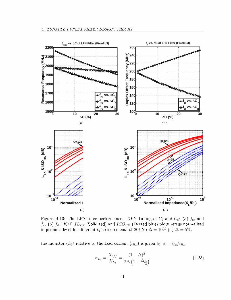
4. TUNABLE DUPLEX FILTER DESIGN: THEORY
0 10 20 301500
1600
1700
1800
1900
2000
2100
2200ftx,rx
vs. ΔC of LFN Filter (Fixed L3)
ΔC (%)
Res
on
ance
Fre
qu
ency
(M
Hz)
frx
vs. ΔC8
ftx
vs. ΔC7
ftx
vs. ΔC8
(a)
0 10 20 30100
120
140
160
180
200
220
240
260fd vs. ΔC of LFN Filter (Fixed L3)
ΔC (%)
Du
ple
x O
ffse
t F
req
uen
cy (
MH
z)
fd vs. ΔC
7
fd vs. ΔC
8
(b)
10−2
10−1
10010
−1
100
101
ILT
X &
ISO
RX (
dB)
Normalised Impedance(XL/R
L)
Q=125
Q=25
Q=125
(c)
10−2
10−1
10010
−1
100
101
ILT
X &
ISO
RX (
dB)
Normalised Impedance(XL/R
L)
Q=25
Q=125
Q=125
(d)
Figure. 4.13: The LFN lter performance- TOP: Tuning of C7 and C8: (a) ftx andfrx (b) fd. BOT: ILTX (Solid red) and ISORX (Dotted blue) plots versus normalisedimpedance level for dierent Q's (increments of 20) (c) ∆ = 10% (d) ∆ = 5%.
the inductor (L3) relative to the load current (iRL) is given by α = iL3/iRL
.
αL3 =Xeff
XL3
=(1 + ∆)2
2∆(1 + ∆/2
) (4.23)
71

4. TUNABLE DUPLEX FILTER DESIGN: THEORY
10−2
10−1
10010
0
101
102
(αL
3) an
d (α
C8)
Fractional Duplex Frequency ( ∆)
αL
3
αC
8
Figure. 4.14: Peak Current through L3 (Solid blue) and C8 (Dotted red) normalisedto the load current versus ∆ for Fig. 4.12.
similarly for capacitor C8
αC8 =Xeff
XC8
=(1 + ∆)
2∆(1 + ∆/2
) (4.24)
which is plotted in Fig. 4.14. The peak current increases as the fractional duplex
frequency reduces. For a 10dB null-depth with a Q of 50 at LTE1, a normalised
impedance level of 0.158 is required and this gives an ILTX of 0.83dB (Fig. 4.13c).
Xeff (obtained from (4.21)) can be used in (4.22) or Fig.4.11 to calculate a peak
voltage across C7 of 9.1V. This is about 18% of that experienced by C1 in the rst
circuit. However, the peak current is considerably increased with the inductor expe-
riencing 1.15A, or αL3 = 5.7 times the load current, compared with αL1 = 1 for the
original LFN circuit. The capacitor C8 carries slightly less current with αC8 = 5.2,
which is close to the voltage magnication of the rst LFN circuit (as would be ex-
pected considering the dual nature of the circuits). The large current magnication
72
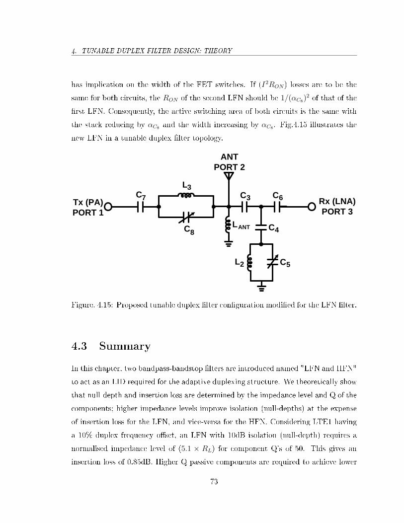
4. TUNABLE DUPLEX FILTER DESIGN: THEORY
has implication on the width of the FET switches. If (I2RON) losses are to be the
same for both circuits, the RON of the second LFN should be 1/(αC8)2 of that of the
rst LFN. Consequently, the active switching area of both circuits is the same with
the stack reducing by αC8 and the width increasing by αC8 . Fig.4.15 illustrates the
new LFN in a tunable duplex lter topology.
C
L
CL
C
Tx (PA)
PORT 1
ANT
PORT 2
Rx (LNA)
PORT 3
3
7
8
3
2
C6
C4
C5
LANT
Figure. 4.15: Proposed tunable duplex lter conguration modied for the LFN lter.
4.3 Summary
In this chapter, two bandpass-bandstop lters are introduced named "LFN and HFN"
to act as an LID required for the adaptive duplexing structure. We theoretically show
that null-depth and insertion loss are determined by the impedance level and Q of the
components; higher impedance levels improve isolation (null-depths) at the expense
of insertion loss for the LFN, and vice-versa for the HFN. Considering LTE1 having
a 10% duplex frequency oset, an LFN with 10dB isolation (null-depth) requires a
normalised impedance level of (5.1 × RL) for component Q's of 50. This gives an
insertion loss of 0.85dB. Higher Q passive components are required to achieve lower
73
4. TUNABLE DUPLEX FILTER DESIGN: THEORY
insertion loss and higher isolation.
There are two possible LFN networks, which are duals of each other. For in-
put powers of 30dBm, one suers from enhanced peak voltages (≈51V), while the
other has enhanced current (≈1.15A) in the resonant circuits. The choice of network
depends on the implementation technology.
If the proposed tunable duplex lters are to be integrated on-chip it is important
to employ a silicon-based technology compatible with existing wireless systems. For
example, wireless front-end modules are implemented on Silicon-on-Sapphire (SOS) or
Silicon-on-Insulator (SOI) technologies due to the low parasitic eect of the substrate
as well as relatively high-Q passive components. These technologies were therefore
chosen.
The next chapter compares Peregrine 0.25µm UltraCMOS and STMicroelectron-
ics 0.13µm HR-SOI processes in terms of process ow, available devices, and RF
switching performance.
74

Chapter 5
Silicon-on-Insulator Technologies
The ever-increasing demand for wireless data bandwidth and the development of the
LTE-Advanced standard has increased the push for higher levels of integration of the
wireless's radio frequency functions. All the while, the ever increasing number of
bands the RF circuits must contend with leads to toughening specications. Today,
the entire radio is contained in a few devices (chips) with some external passive
components. There are two major silicon technologies found in every corner of a
mobile handset, Bulk CMOS (Complementary Metal-Oxide Semiconductor) and SOI
(Silicon-on-Insulator).
SOI technology has been around since the 1960s when the rst so-called silicon-on-
sapphire (SOS) process was introduced. It diers from the traditional bulk CMOS
process due to the presence of a buried oxide layer under the active area of the
silicon substrate, which forms a dielectric-ally isolated transistor [58]. This oxide
layer has a very important impact on the physical behaviour of MOS transistors
and the provided benets are numerous such as improved immunity to radiation and
latch-up phenomena, lower leakage currents and lower junction capacitances.
SOI was rst studied for hardening circuits such as spacecraft electronics and
devices operating in a radiative nuclear environment. However, the poor quality of
SOI materials had long limited its industrial development for the electronics consumer
75
5. SILICON-ON-INSULATOR TECHNOLOGIES
market. Improving the quality of the buried oxide of thin silicon lms on top of an
insulator recently revived interest in the technology [59]. In the eyes of industry, it has
many advantages in terms of integration, power consumption and immunity to soft
errors. Unlike the Bulk CMOS process, it is only in recent years that SOI technology
has found its pathway into cellular phones. The low parasitics of SOI have recently
been exploited as a switching technology for RF signals. It is now replacing GaAs
technology in the RF front-end of mobile phones.
This chapter focuses on SOI/SOS technology and its properties. Section 5.1 ad-
dresses the realization of SOI materials, giving the main fabrication methods and
the latest technology. Section 5.2 briey compares Bulk CMOS technology with the
SOI/SOS processes. Peregrine UltraCMOS and STMicroelectronics HR-SOI process
features are briey discussed in Section 5.3 and Section 5.4, respectively. Section
5.5 presents the basic theory and resulting design compromises regarding RF FET
switches. The trade-o between the latter's power handling capability, linearity and
insertion loss is provided for the SOS case. The gure of merit (FOM) for a FET
switch is dened, then SOS and SOI structures are compared. Keysight ADS software
and SOI/SOS PDKs are used to obtain the simulation results. A summary in Section
5.6 concludes the chapter.
5.1 SOI Fabrication Process: Background
The SOI substrate has a tri-layer structure, consisting of thick silicon, an insulator
(note BOX for "Buried Oxide") and the active silicon layer [60]. The last layer forms
the conduction area on which the transistors are dened. In practice, the SOI term
is usually reserved for a substrate consisting of a layer of silicon over a silicon-oxide
(SiO2) layer, itself located on a silicon substrate. This structure is most common
because it is the easiest to make, and the more economical to produce.
The presence of an insulating buried layer under the silicon lm induces signicant
dierences between the operation of the transistor on bulk silicon and the transistor
76

5. SILICON-ON-INSULATOR TECHNOLOGIES
on SOI. The rst commercial use of the latter was motivated by the need to obtain
more resistant devices to radiation [61,62] for space and military applications. These
radiations can excite the atoms of silicon and generate latch-up in standard CMOS
processes. In SOI, only the thin top layer of silicon (lm or active area) of the wafer
is used. Insulation made by the BOX, between the active region and the rest of the
substrate, minimizes the risk of malfunction of the circuit by the excitation of atoms,
under the transitory eect of radiation. SOI entered the world of commercial micro-
electronics because of increased performance compared to the bulk silicon technology.
This is evident at high frequencies where reduced parasitics and reduced substrate
losses improve performance. Table 5.1 summarises the main pros and cons of SOI
devices.
Table 5.1: Summary of SOI process features.
Advantages Disadvantages+ Isolation between the devices - Floating substrate eect+ Reduction of parasitic capacitances - Self-heating eect+ Less parasitic leakage currents ofjunction substrate
- Existence of the parasitic lateralbipolar transistor
+ Reduction of the short channel eect- Relatively large contact resistance(for thin STI layer)
+ Decreasing the polarization eect ofthe substrate
- Reduced drain breakdown voltage
+ Limited vertical area of theSource/Drain+ Tolerance to radiation and relativelyhigh temperature
In the past ve years, the semiconductor industry has seen dierent SOI substrate
avours such as silicon-on-insulator, silicon-on-sapphire (SOS) and high-resistivity
SOI substrates (HR-SOI). These enable higher performance at reduced overall sys-
tem cost and footprint. SOI substrates can be manufactured by three techniques,
oxygen implant/anneal (SIMOX) method, bonding-and-etched-back-SOI (BESOI),
and UNIBOND (Smart-Cut).
77

5. SILICON-ON-INSULATOR TECHNOLOGIES
5.1.1 The SIMOX Method
The SIMOX ("Separation by IMplantation of OXygen") method [6] consists of two
steps. First, oxygen ions are implanted in the substrate surface, and thereafter,
annealing at high temperature (1300-1350°C) forms the BOX. The BOX thickness
is determined by the implanted dose and its energy. Although this method was
developed in the late 1970s [63], the rst SIMOX substrate were marketed in 2000.
Mass production was linked to the development of a machine capable of implanting
oxygen ions without contaminating the substrate at very high energy and dose. For
instance, forming a 400nm BOX and a silicon (Si) lm of 200nm requires oxygen
implantation of 2× 10¹⁸ /cm3 at an energy of 180keV. Since the demand for thinner
BOX layer of 80nm were placed in 1990s, the implantation dose were decreased to
4×10¹⁷ /cm3. Furthermore, the implantation energy was lowered to 70KeV to obtain a
thin active lm of 50nm for fully-depleted transistors. Currently, the SIMOX method
provides SOI substrate with uniform thickness of ±10nm for the BOX and ±5nm for
the Si lm.
5.1.2 The BESOI Method
The bonding-and-etched-back-SOI (BESOI) technique, as an alternative to SIMOX,
has the advantage of a cleaner interface between the silicon and oxide layers with less
defects and charge-up eects at the buried oxide [64]. The above fabrication uses
a material which is generated by oxidizing the seed and/or handle wafers, followed
by bonding the two wafers. The active device region is created on the seed wafer by
lapping and etching to the desired lm thickness. Even though this method is suitable
for the fabrication of 600nm SOI, the presence of an etch stop layer is essential to
achieve SOI wafers with a nominal thickness of 500nm or less [60].
78
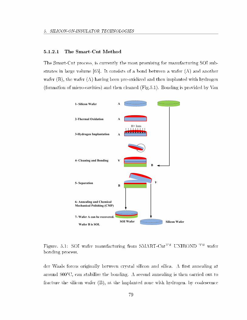
5. SILICON-ON-INSULATOR TECHNOLOGIES
5.1.2.1 The Smart-Cut Method
The Smart-Cut process, is currently the most promising for manufacturing SOI sub-
strates in large volume [65]. It consists of a bond between a wafer (A) and another
wafer (B), the wafer (A) having been pre-oxidized and then implanted with hydrogen
(formation of micro-cavities) and then cleaned (Fig.5.1). Bonding is provided by Van
H+ Ions
A
A
A
A
B
B
A
SOI Wafer Silicon Wafer
1- Silicon Wafer
2-Thermal Oxidation
3-Hydrogen Implantation
4- Cleaning and Bonding
5- Separation
6- Annealing and Chemical Mechanical Polishing (CMP)
7- Wafer A can be recovered. Wafer B is SOI.
Figure. 5.1: SOI wafer manufacturing from SMART-CutTM UNIBOND TM waferbonding process.
der Waals forces originally between crystal silicon and silica. A rst annealing at
around 800°C, can stabilize the bonding. A second annealing is then carried out to
fracture the silicon wafer (B), at the implanted zone with hydrogen, by coalescence
79
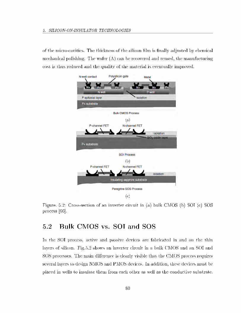
5. SILICON-ON-INSULATOR TECHNOLOGIES
of the micro-cavities. The thickness of the silicon lm is nally adjusted by chemical
mechanical polishing. The wafer (A) can be recovered and reused, the manufacturing
cost is thus reduced and the quality of the material is eventually improved.
(a)
(b)
(c)
Figure. 5.2: Cross-section of an inverter circuit in (a) bulk CMOS (b) SOI (c) SOSprocess [66].
5.2 Bulk CMOS vs. SOI and SOS
In the SOI process, active and passive devices are fabricated in and on the thin
layers of silicon. Fig.5.2 shows an inverter circuit in a bulk CMOS and an SOI and
SOS processes. The main dierence is clearly visible that the CMOS process requires
several layers to design NMOS and PMOS devices. In addition, these devices must be
placed in wells to insulate them from each other as well as the conductive substrate.
80
5. SILICON-ON-INSULATOR TECHNOLOGIES
Eventually, the wells need to be biased to a reverse potential in order to reduce
the parasitics. The SOI/SOS process takes advantage of its simplicity to reduce the
number of fabrication masks for the same inverter circuit. It is noteworthy to mention
that the SOS active devices are developed in an ultra-thin (100nm) silicon (UTSi)
lm grown on top of a crystallised sapphire (Al2O3) substrate. The method has been
patented by Peregrine Semiconductor Corp. [67]. The work in this thesis uses the
250nm SOS Peregrine process and the 130nm SOI process of STMicroelectronics.
5.3 Peregrine SOS Process Features
Peregrine oers several varieties of UltraCMOS processes targeting wireless infrastruc-
ture, land-mobile-radios, automotive, military, radar and space. Each process option
includes three aluminium metallisations, where the top metal thickness is 3.1 µm for
FC, GC, and PC processes. This top conductor is often used to design relatively
low-ESR interconnects and inductors. Metal-Insulator-Metal (MIM) capacitors are
also formed between the two top metallisations. Table 5.2 summarises key features
of the process options.
Since shorter gate lengths are preferable in the design of any switching application,
the UltraCMOS GC process is chosen for this research work. There are 9 types of eld-
eect transistors (FET) in that process variant: 5 dierent N-channel and 4 dierent
P-channel transistors covering three Vt settings and a thick oxide variant. These
devices could potentially be used for RF and high-performance digital low-leakage
applications. The transistor types and their specications are shown in Table 5.3.
TIN devices were used in this work because the thick oxide increased the voltage
breakdown. The near zero Vt lowered the Ron but necessitated the use of a −ve gatevoltage to switch the device o.
81
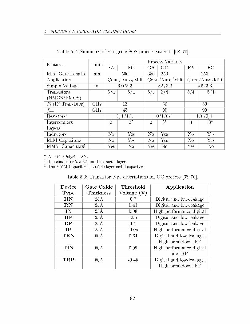
5. SILICON-ON-INSULATOR TECHNOLOGIES
Table 5.2: Summary of Peregrine SOS process variants [6870].
Features UnitsProcess Variants
FA FC GA GC PA PCMin. Gate Length nm 500 350 250 250Application Com./Auto/Mili. Com./Auto/Mili. Com./Auto/Mili.Supply Voltage V 3.0/3.3 2.5/3.3 2.5/3.3Transistors(NMOS/PMOS)
5/4 5/4 5/4 5/4 5/4 5/4
Ft (IN Transistor) GHz 15 30 30fmax GHz 45 90 90Resistors* 1/1/1/1 0/1/0/1 1/0/0/1InterconnectLayers
3 3 3 3* 3 3*
Inductors No Yes No Yes No YesMIM Capacitors No Yes No Yes No YesMMM Capacitors Yes No Yes No Yes No
* N+/P+/Polycide/SN. Top conductor is a 3.1 µm thick metal layer. The MMM Capacitor is a triple layer metal capacitor.
Table 5.3: Transistor type descriptions for GC process [6870].
DeviceType
Gate OxideThickness
ThresholdVoltage (V)
Application
HN 25Å 0.7 Digital and low-leakageRN 25Å 0.43 Digital and low-leakageIN 25Å 0.08 High-performance digitalHP 25Å -0.6 Digital and low-leakageRP 25Å -0.41 Digital and low-leakageIP 25Å -0.05 High-performance digital
TRN 50Å 0.64 Digital and low-leakage,High breakdown RF
TIN 50Å 0.09 High-performance digitaland RF
TRP 50Å -0.45 Digital and low-leakage,High breakdown RF
82
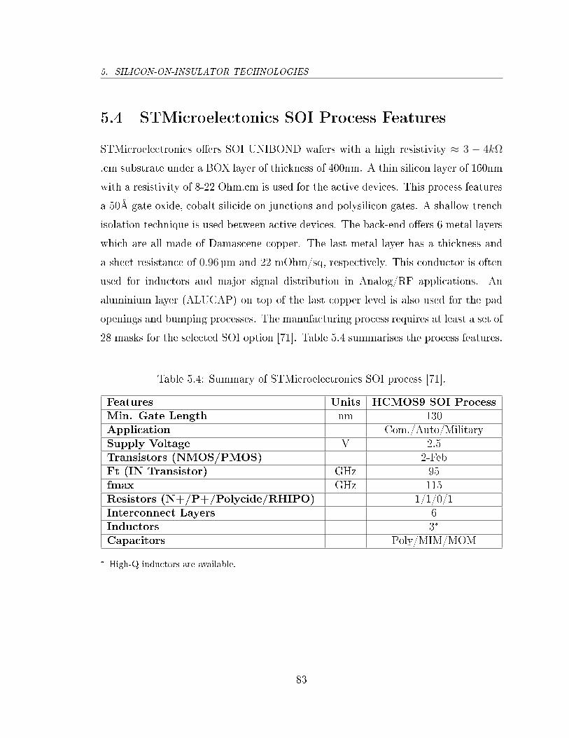
5. SILICON-ON-INSULATOR TECHNOLOGIES
5.4 STMicroelectonics SOI Process Features
STMicroelectronics oers SOI UNIBOND wafers with a high resistivity ≈ 3 − 4kΩ
.cm substrate under a BOX layer of thickness of 400nm. A thin silicon layer of 160nm
with a resistivity of 8-22 Ohm.cm is used for the active devices. This process features
a 50Å gate oxide, cobalt silicide on junctions and polysilicon gates. A shallow trench
isolation technique is used between active devices. The back-end oers 6 metal layers
which are all made of Damascene copper. The last metal layer has a thickness and
a sheet resistance of 0.96µm and 22 mOhm/sq, respectively. This conductor is often
used for inductors and major signal distribution in Analog/RF applications. An
aluminium layer (ALUCAP) on top of the last copper level is also used for the pad
openings and bumping processes. The manufacturing process requires at least a set of
28 masks for the selected SOI option [71]. Table 5.4 summarises the process features.
Table 5.4: Summary of STMicroelectronics SOI process [71].
Features Units HCMOS9 SOI ProcessMin. Gate Length nm 130Application Com./Auto/MilitarySupply Voltage V 2.5Transistors (NMOS/PMOS) 2-FebFt (IN Transistor) GHz 95fmax GHz 115Resistors (N+/P+/Polycide/RHIPO) 1/1/0/1Interconnect Layers 6Inductors 3*
Capacitors Poly/MIM/MOM
* High-Q inductors are available.
83

5. SILICON-ON-INSULATOR TECHNOLOGIES
5.5 SOI/SOS FET Switch Performance
When a FET operates as a switch, it is biased in strong inversion, and is characterised
by its on-resistance (Ron) and o-capacitance (Coff ). Fig.5.3 shows an RF FET
switch with its equivalent circuit in ON and OFF states. The gate bias resistance
G
D
S
RGRDS
VBias
RF+
RF-
(a)
G
D
S
RonCGS
CGD
(b)
G
D
S
CoffCGS
CGD
RDS
(c)
Figure. 5.3: Circuit model of (a) switch (SW) FET (b) FET equivalent model in theON-state (c) FET equivalent model in the OFF-state.
(RG) should be much higher than the parasitic capacitances of the transistor, (Coff ),
dened as the series combination of CGS and CGD in parallel with CDS. In the on-
state of a series connected (oating) device, a small value of RG would cause loss due
to a large current owing through the parasitic capacitances to AC ground [72]. In
addition, small RG prevents the proper voltage division in o-state across CGS and
CGD, resulting in a reduction in the 1dB compression point and sacricing the switch
linearity. The importance of this gate resistor RG will be covered in detail in Section
5.5.1.
Insertion loss and isolation are key parameters that indicate the eciency of a
single FET switch which can be approximated by the Ron × Coff gure of merit
(FOM) [73]. Nowadays, the SOI manufacturers put much eort into scaling down
this gure. The smaller FOM the better RF switching performance. The rst task
of this research was to investigate the Ron and the Coff per millimetre FET gate
84

5. SILICON-ON-INSULATOR TECHNOLOGIES
AC
50Ω G
D
SDC
W=1000µm
L=0.25µm
Z11
AC
50Ω G
D
SDC
W=1000µm
L=0.28µm
Z11
Figure. 5.4: A switch FET test circuit: SOI process (left) and SOS process (right).
width at cellular frequencies. Fig.5.4 shows the test circuit in a 50Ω system. The
aforementioned fundamental parameters of a switch FET are given by
Ron = Re (Z11) |ON−state (5.1)
Coff =1
2πf × Im (Z11) |OFF−state(5.2)
Table 5.5 compares the (Ron ×Coff ) FOM from the 130nm SOI and the 250nm SOS
process technologies at 2GHz. The improved FOM of the more modern 130nm SOI
technology is predominantly due to a lower on-resistance. The work in this thesis
used both technologies.
Table 5.5: Survey of FOM from the SOI and the SOS technologies at 2GHz.
Process Technology Ron (Ω/mm) Coff (fF/mm) Ron × Coff (fs)130nm SOI 1.0 278 278250nm SOS 1.6 280 448
A small FOM results in less insertion loss and a higher linearity. The insertion
loss of a switch is given by:
IL (dB) = 20 log10
(1 +
Ron
2R0
)(5.3)
Where R0 is the impedance of the source and load in a 50Ω system. Using 250nm SOS
85

5. SILICON-ON-INSULATOR TECHNOLOGIES
Figure. 5.5: The on-resistance of a 58 nger device as a function of the gate voltage(VBias) and FET periphery (nger width).
technology with an oxide thickness (tox) of 50Å and W = 2.75mm, a single optimised
switch has an Ron equal to 1.55Ω and Coff to 782.5fF , resulting in an insertion loss
of 0.133dB at V g = 2V . The Ron is varied by the applied DC gate voltage (VBias)
and the periphery (W) of the switch. Fig.5.5 illustrates the reduction of Ron as a
function of increasing VBias and W with an identical number of 58 ngers.
There are two common measures of distortion, third order intercept point (IP3)
and the 1dB compression point (P1dB). The former is measured by applying two
closely spaced tones to the switch under test and measuring the generated third and
higher order products. The third order intercept point (IP3) is dened where the
input and distortion powers are equal [74]. The latter is the measured output level
where it is a 1dB deviated from the linear gain.
86
5. SILICON-ON-INSULATOR TECHNOLOGIES
Intermodulation products (IMP) are created due to the non-linearity of the switch.
In order to guarantee the performance in wireless applications, the transmitted power
via a turned-on switch should not be distorted. The third order intermodulation
harmonic power should be 60dB less than the power of the desired signal for a typical
handheld device [75].
Two compression points can be distinguished for a switch. The rst (P1dBV th)
results from high power transmissions through an ON device. The second (P1dBbk)
occurs when the drain and the source voltages exceed the breakdown conditions in the
OFF state. For the given periphery and biasing voltage of the above switch, P1dBV th
and P1dBbk are 25.81dBm and 18.78dBm, respectively.
5.5.1 Biasing Considerations
The bias network determines ve important operating features of an RF FET switch,
which are the minimum operating frequency (fmin) of the switch, the switching time
(τ), ohmic losses in the bias network, the maximum power handling (Pmax), and the
uniformity of distributed voltage across the transistor during switching states. Among
dierent bias network topologies fabricated on silicon substrates, the resistive one is
the most suitable network in terms of high yield and compactness. SOS technology
provides a diusion resistor with large sheet resistance of 2500 Ωsqr, enabling a large
resistance value occupying a small area. The switching time for the above FET tran-
sistor (Fig.5.3) is given by τ = RCg where Cg is the eective capacitance connected
to the gate node, dened as the parallel value of CGS and CGD in the o-state. This
time constant establishes the simultaneous switching condition in stacked transistors.
The bias resistor plays a vital role in aecting the minimum operating frequency
(fmin) of the switch, estimated as:
fmin ≈7
πRCg
(5.4)
As described earlier, the OFF state voltage swing should be divided equally between
87

5. SILICON-ON-INSULATOR TECHNOLOGIES
drain-to-gate (VDG), and drain-to-source (VDS). For a single FET, this voltage swing
is derived as [76]:
VDG
VDS
=
(1 + (πf RCg)
2
1 + 4 (πf RCg)2
) 12
(5.5)
Where f is the frequency at which the switch operates. Note that VDG cannot exceed
its breakdown value which is dened as (VDGbk−Vth)/2, where VDGbk and Vth are the
drain-to-gate breakdown and threshold voltages, respectively. This limitation for a
SOS transistor (tox = 50Å) with intrinsic threshold voltage is 1.33V . In practice, the
maximum voltage across the drain-to-source (VDSM) must be less than the (VDSbk −Vth), so that the gate resistor value can be derived from:
R =1
πf Cg
1− 4(VDSM
VDSbk− Vth
)2
4[(
VDSM
VDSbk− Vth
)2− 1
]
12
(5.6)
The gate voltage swings superposed on the gate DC supply voltage can reach
up to half of VDSM because the gate-to-source and gate-to-drain impedances are
equal. During the rst half of the period, the gate voltage should not fall below the
threshold voltage. Moreover, the drain-gate voltage should not exceed its breakdown
value during the whole cycle. These two constraints lead to:
VDSM = VDGbk − Vth (5.7)
VBias(max) =VDGbk + Vth
2(5.8)
The maximum power handling capability of a single FET switch is given by:
Pmax =(VDSbk − Vth)2
2R0
(5.9)
For a given SOS transistor, the power magnitude of 139mW can be handled by a
single transistor. The dissipated power in the bias network is inversely related to the
88

5. SILICON-ON-INSULATOR TECHNOLOGIES
gate resistor: a larger value reduces the power dissipation but degrades the switching
speed.
G
D S
RG
RDS
G
D S
RG
RDS
G
D S
RG
RDS
G
D S
RG
RDS
G
D S
RG
RDS
G
D S
RG
RDS
G
D S
RG
RDS
G
D S
RG
RDS
RF+ RF-
VBias
M1M2M3M4M5M6M7M8
Figure. 5.6: Stacking FET's approch.
5.5.2 Stacking FET's Approach
To achieve the required high power handling in cellular systems such as GSM (35dBm),
a stacked conguration of n FETs can be used. While this improves the switch's abil-
ity to handle power as well as increases the 1dB compression point, the total insertion
loss is degraded. The following expressions apply for eight (n = 8) stacked transistors
with the above periphery (Fig.5.6). The periphery is dened as the number of gate
ngers times the unit gate width.
IL (dB) = 20 log10
(1 +
nRon
2R0
)−→ ILn=8 = 1 dB (5.10)
P1dBVth(dBm) = 10 log10
(2(n(Vth−VOFF ))2
R0
)+ 30
−→ P1dBVth= 38.74 dBm
(5.11)
P1dBbk (dBm) = 10 log10
((nVbk)2
2R0
)+ 30
P1dBbk = 36.84 dBm(5.12)
When stacking n identical FET switches, the minimum value of the combined gate
resistor (Rmin) is a function of the individual gate resistors (R), and can be calculated
89

5. SILICON-ON-INSULATOR TECHNOLOGIES
by:
Rmin =R (2n− 1)
n(5.13)
Therefore, the minimum time constant that turns on all the stacked FET's simul-
taneously can be derived from:
τmin = (2n− 1)RCg (5.14)
ON-OFF transient characteristics were simulated to guarantee breakdown compliance
when switching at dierent phases of the RF carrier. Fig.5.7 illustrates the simulated
o-state voltages of the drain node, drain-to-source, gate-to-source, and gate-to-drain
of M1-M8 at a maximum input power of 39.5dBm. The maximum drain voltage in
the o-state [with the gate bias of −1.5V ] translates to 21.1V . Regardless of this; the
peak voltage drops across each transistor's terminals should remain below 2.6V to
avoid breakdown phenomena, allowing the whole stack to withstand a large voltage
swing before any switch breaks down. The number of stacked transistors can be
obtained from the peak RF voltage across the switch divided by the drain-source
breakdown voltage (suciently de-rated for safety margin). The gate voltage of 2.5V
combined with the periphery (width) of each transistor keeps the total on-resistance
as low of 1.55Ω/transistor in the saturation regime [76].
Fig.5.8 shows the compression behaviour of the ON current through the stacked
transistors at 2GHz. As can be observed in this gure, a 1dB gain compression point
of 49.2dBm is achieved. At this power level the switches would be operating above
their breakdown voltage if taken to the OFF condition. A two-tone test signal with
a frequency spacing of 10MHz resulted in an extrapolated input IP3 measurement
of 54.3dBm.
Fig.5.9 illustrates the linearity and intermodulation trend of the conguration.
The above (P1dB) measurement appears too high for the IP3 result; (as a rule of thumb
the P1dB measurement is ≈ 15dB below the IP3). Discussions with the Engineers at
90

5. SILICON-ON-INSULATOR TECHNOLOGIES
(a) (b)
(c) (d)
Figure. 5.7: Voltage distribution for eight stacked SOS FET's switches when theinput power hits 39.5dBm. (a) Voltage waveforms at dierent drain nodes (VD)of transistors M1-M8, (b) Drain-to-source Voltages (VDS1 ∼ VDS8). (c) Gate-to-source voltages (VGS1 ∼ VGS8). (d) Gate-to-drain voltage waveforms (VGD1 ∼ VGD8).Simulations in ADS (Advanced Design System) using TIN device models.
Peregrine indicated that the cause was most likely due to poor non-linearity models
in the Peregrine PDK at high power levels.
91
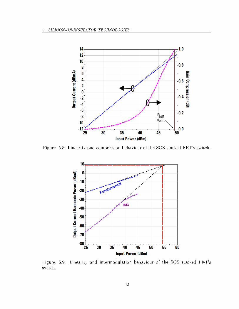
5. SILICON-ON-INSULATOR TECHNOLOGIES
Figure. 5.8: Linearity and compression behaviour of the SOS stacked FET's switch.
Figure. 5.9: Linearity and intermodulation behaviour of the SOS stacked FET'sswitch.
92
5. SILICON-ON-INSULATOR TECHNOLOGIES
5.6 Summary
In this chapter, we presented the materials and industrial techniques for manufac-
turing SOI substrates. This eliminates the intrinsic parasitic eects of the silicon
substrate for RF applications. SOI technology has superior features such as immu-
nity to coupled noise and a reduction in the short channel eect [60]. The technology
is therefore a prime candidate to continue the downscaling of RF passive compo-
nents with the goal of a single chip RF front-end solution. Two world leading SOI
technologies, 130nm SOI and 250nm SOS processes, were compared. Both processes
oer relatively high quality-factor (Q) inductors and capacitors as a result of the high
resistivity substrate [66,77].
We chose the above processes to investigate their RF switching performance for the
described tunable duplex lters of the previous chapter. As mentioned in Chapter 4,
FET switches are the key elements of a digital switched capacitor bank. Therefore, the
design fundamentals of a FET switch was explained, emphasising the on-resistance,
o-capacitance, insertion loss, linearity and biasing. High power handling requires
a stacked conguration. Keysight ADS software with a Peregrine PDK are used to
simulate the operation of a switch with eight stacked FETs, with a transmitter power
of 36.5dBm. The simulated P1dB and IIP3 were somewhat approximate at 49.2dBm
and 54.3dBm respectively, due to poor simulation models at these powers.
The remainder of the Thesis describes four implementations of the LID circuit:
three fully integrated solutions as well as a discreet solution with o-the-shelf com-
ponents. The next Chapter describes single band LID solutions.
93
Chapter 6
Single-Band Tunable Duplex Filter:
Implementation
A low isolation device is an essential building block of the adaptive duplexer. This
chapter studies the feasibility of implementing channel selectable lters in a fully in-
tegrated Silicon-on-Sapphire (SOS) solution and a partially integrated solution using
o-chip PCB components. Digitally switched capacitor banks (DSCBs) are employed
to tune the LID to the desired channel of LTE band 1. The tunable capacitor is part
of the resonant circuit, therefore, a large peak voltage appears across the FET device.
Since the FET switch has a breakdown voltage of less than 3V, FETs are stacked to
handle the higher peak voltages.
Section 6.1 describes an integrated solution for a single-band tunable LID. Impor-
tant design aspects of the DSCB are highlighted. The Peregrine SOS process is used
for fabrication. A discrete solution is provided in section 6.2 using high-Q compo-
nents on a multilayer FR-4 PCB. The performance of these solutions are compared.
A summary (section 6.3) concludes the chapter.
94

6. SINGLE-BAND TUNABLE DUPLEX FILTER: IMPLEMENTATION
0
1
2
h1
Canceller
Control
h2
Duplexing Filter
Gain &
Phase Adj.
Time
Delay
Time
Delay
Antenna
Error Signal e1Error Signal e2
Cross
Correlation
Cross
Correlation
Data
Enc.Rx Data
Dec.Tx
Tx RxPilot
Gen.Tx Residue
ReceiverPilot Tx
(Very Low
Power)
Txf
Txf
Rxf
Rxf
Pilot Reference (@ )Rxf
Tx Reference (@ )Txf
Pilot Residue (@ )Rxf
Tx Residue (@ )Txf
Mobile Station
(MS) Tx Chain
Mobile Station
(MS) Rx Chain
Base
Station
(BS)
Tx (@ )
MS -> BSTx
f
Rx (@ )
BS -> MSRx
f
This Work
Figure. 6.1: Adaptive duplexer architecture. (The wideband circulator is replaced byL-C duplexing lters.)
6.1 SOS Duplex Filters: Overview
Fig.6.1 illustrates a detailed block diagram of the adaptive duplexer for a two loop
cancellation path described in Chapter 3. In this work, the circulator is replaced
by a tunable set of L-C duplex lters which enable the scheme to cover multiple
channels and bands. The duplex lter (Fig.6.2) was designed to operate at LTE1,
which has a relatively large duplex oset of 190 MHz. According to (4.8) and (4.15),
the selected capacitance ratios (C1/C2) and (C4/C5) for this frequency band are 0.191
and 0.175, respectively. The Peregrine 0.25-µm UltraCMOS SOS process was chosen
for implementation due to the low parasitic capacitances, relatively high-Q inductors
95

6. SINGLE-BAND TUNABLE DUPLEX FILTER: IMPLEMENTATION
Figure. 6.2: Single-band tunable SOS duplex lter.
and a high linearity performance. Since the purpose of this implementation was
to study the limitations of an on-chip solution for a duplex lter; on-chip passive
elements were used. SOS metal-oxide-metal (MIM) capacitors can tolerate a peak
voltage of 15V. Therefore, both capacitors as well as FET's need to be stacked.
6.1.1 Digitally Switched Capacitor Bank (DSCB)
A series connection of a xed MIM capacitor and NMOS switch forms a switched
capacitor (SC). The main performance metrics of the SC are the Q in both OFF and
ON states, and the achievable capacitance ratio (Con/Coff ). A simplied model of a
3-bit DSCB is shown in Fig.6.3. The MIM capacitor values and the FET transistor
sizes are weighted in a binary manner. For instance, the least-signicant capacitor C1
is designed to have the lowest capacitance of CLSB. The next capacitor, C2, should
have a capacitance value of twice CLSB. In general, each signicant capacitor has
96

6. SINGLE-BAND TUNABLE DUPLEX FILTER: IMPLEMENTATION
C1
SW FET1
C2
SW FET2
C3
SW FET3
RF+
RF-
(a)
Coff Ron/4 4Coff
Bit2
4C MIM
Ron/2 2Coff
Bit1
2C MIM
Ron
Bit0
C MIM
RF-
RF+
(b)
Figure. 6.3: 3-bits DSCB (a) simplied model (b) model in ON and OFF conditions.
a value that is twice that of the previous signicant capacitor. Finally, the most
signicant capacitor should have a value of 2(b−1) × CLSB, where b is the number
of bits. The size of FET's are accordingly binary weighted to the respective series
MIM capacitor. Assuming that CMIM is much larger than Coff and its parasitic
resistance is not also comparable with the Ron, the (Con/Coff ) and the Qmin of the
least-signicant bit (LSB) are given by
Con
Coff
=Cmax
Cmin
= 1 +CMIM
Coff
(6.1)
Qmin =1
ωCMIMRon
=1
ω(Cmax
Cmin− 1
)RonCoff
(6.2)
where ω is the operating frequency of the DSCB. Generally, the capacitance ratio is
set by a desired Qmin and vice versa per the following equations.
Con
Coff
= 1 +1
ωQminFOM(6.3)
97

6. SINGLE-BAND TUNABLE DUPLEX FILTER: IMPLEMENTATION
Qmin =1
ω × FOM ×(
Con
Coff− 1
) (6.4)
The two above equations indicate the limitation of the (Con/Coff ) based on process
and the Q requirement. Considering the 250nm SOS process, Table.6.1 summarises
the (Con/Coff ) for dierent Qmin at four common LTE frequencies.
Table 6.1: Required (Con/Coff ) for dierent Qmin across four common LTE frequen-cies.
Frequency(MHz)
(Con/Coff)Qmin = 50
(Con/Coff)Qmin = 70
(Con/Coff)Qmin = 100
900 8.89 6.64 4.951800 4.95 3.82 2.972200 4.23 3.31 2.613700 2.92 2.37 1.96
The DSCB is usually used in series or parallel with an inductor. Therefore, its
Q-factor becomes prominent and has a major impact on the total Q of the tank
resonator. On the other hand, the above results clearly indicate that the (Con/Coff )
shrinks when frequency increases at constant Qmin. A rational trade-o is a must
when larger (Con/Coff ) is required i.e. switch between frequency bands.
The peak voltage across the FET switch could be much higher than the rated
voltage at the resonance. Consequently, stacking n number of FET's could prevent
breakdown. The eective number of FET's in the stack is determined by
neff = n+Coff
CMIM
(6.5)
The simulated performance of a 3-bit DSCB is shown in Fig. 6.4. The device
widths are scaled to maintain the same (Con/Coff ) ratio for each bit. The RonCoff
gure of merit for this process is 448fs. The leakage capacitance Coff in series with
the MIM capacitor reduces the voltage across the stack in the OFF state. In this case,
the SC peak voltage can be increased by 27to 24 V when a stack of seven TIN thick-
oxide (tox = 50Å, BVDS = 2.75V ) transistors is used [78]. The series MIM capacitors
98

6. SINGLE-BAND TUNABLE DUPLEX FILTER: IMPLEMENTATION
B0B1B2
Rgate
Rgate
Rgate
Rgate
Rgate
Rgate
Rgate
Rgate
Rgate 1X 2X 4X
RF IN
RF OUT
M1
M6
M7
M1
M6
M7
M1
M6
M7
4C2C1C
(a)
0
10
20
30
40
50
0.7
0.8
0.9
1.0
1.1
0 2 4 6 8
To
tal
Qu
ali
ty-F
ac
tor
To
tal
Ca
pa
cit
an
ce
(p
F)
Cap Setting
Total Capacitance
Total Quality-Factor
Slope = 31fF/step
(b)
Figure. 6.4: 3-bit DSCB: (a) 7 FET stack (b) capacitance control range and Q.
99
6. SINGLE-BAND TUNABLE DUPLEX FILTER: IMPLEMENTATION
are used for the 1C, 2C, and 4C in the DSCB for similar voltage reasons. The gate
bias resistor should be much larger than the resistance of the leakage capacitances
(Rgate >> XCGD) for uniform voltage division across the stack and good Qoff and
Qon performance (section 5.6). However, Rgate should also be small for high switching
speed and low footprint. An Rgate of 20kΩ was chosen, resulting in a Qoff , Qon, and
(Con/Coff ) of 42, 32, and 1.3, respectively. A negative gate control voltage improved
linearity in the o condition due to the near zero threshold voltage of the transistor,
but was limited to the -2.75V NMOS breakdown.
6.1.2 Pad-based ESD Protection Circuitry
An Electrostatic Discharge (ESD) device protects the circuit from any unwanted large
pulse from environmental or peripheral sources. Generally, the principle behind ESD
protection is to create a low-impedance discharge path between any two pins. This
shunts ESD current and clamps the pad voltages to a suciently low level [79,80].
The protection performance is impacted by the particular mechanism, process
technology, parasitic eects, and resistance of the ESD device. The protection device
introduces parasitic eects that degrade the normal operation of the circuit, in par-
ticular at RF. Parasitics are often due to inappropriate layout design such as spacing
between the tracks and so forth. If the impedance of the ESD discharge path is not
signicantly lower than that of the main circuit path, the voltage strike might not
have enough suppression. It is therefore vital to have a wide metal track to take the
ESD current and a low resistance ESD protection device. Larger device sizes lower
the resistance but increase the parasitics. Therefore, there is a trade-o between the
parasitic eect and ESD current handling capability.
To protect the DSCBs from any unforeseen electrostatic charge, a special pad-
based ESD protection was designed, due to the passive nature of the LID circuit (no
supply voltages). The traditional diode clamps to Vdd and ground cannot be used.
The control voltages must swing to both +ve and -ve values during normal operation.
100

6. SINGLE-BAND TUNABLE DUPLEX FILTER: IMPLEMENTATION
Fig.6.5 shows the proposed ESD protection circuitry. It includes two current paths,
each one composed of large ESD diodes (160 µm) connected to a clamp (480µm),
which ensures protection during negative and positive ESD events.
+V0V
Clamp
Clamp
RESD
Diode
ESD Diode
PAD Internal Circuit
IESD
IESD
(a)
Clamp
Clamp
RESD
Diode
ESD Diode
-V
0V
PAD Internal Circuit
IESD
IESD
(b)
(c)
Figure. 6.5: Pad-based ESD protection circuitry: the path of ESD current pulseduring a (a) positive (b) negative ESD event, (c) ESD layout.
6.1.3 Simulation Results
RF circuit design for cellular frequencies requires fairly accurate modelling of active
and passive devices as well as interconnects. In this work, parasitics of FET switches
are extracted by Cadence software. Scattering parameters for the interconnects are
extracted by ADS momentum and are then included into the nal simulation in
Cadence. Fig.6.6 shows the nal layout and the frequency response of the duplex
lter with all passive components and the layout extracted DSCB's. The Tx null of
101

6. SINGLE-BAND TUNABLE DUPLEX FILTER: IMPLEMENTATION
(a)
-20
-18
-16
-14
-12
-10
-8
-6
-4
-2
0
1.0 1.2 1.4 1.6 1.8 2.0 2.2 2.4 2.6 2.8 3.0
|S21
| & |S
32| &
|S13
| (d
B)
Frequency (GHz)
IL(TX)IL(RX)ISO(TX-RX)
(b)
Figure. 6.6: Single-band tunable duplex lters: (a) nal layout (b)post-layout simu-lation when DSCB's are OFF.
17.5dB is close to the required specs but the Rx null is 14dB. However, the latter
is a less critical specication compared to the Tx null-depth [8]. Insertion losses are
3.8dB and 4.8dB for the Tx and Rx, respectively. The circuit appears to marginally
102

6. SINGLE-BAND TUNABLE DUPLEX FILTER: IMPLEMENTATION
outperform the the calculated values in Table 4.1, with Q=25. The simulated Rx
isolation is 1dB worse but the Tx insertion loss is 1dB lower than the calculated
4.9dB. The analysis assumed all components had the same Q which is clearly not the
case for the circuit, where each component is designed to have as high a Q as possible
within the constraints of chip area and process characteristics.
103
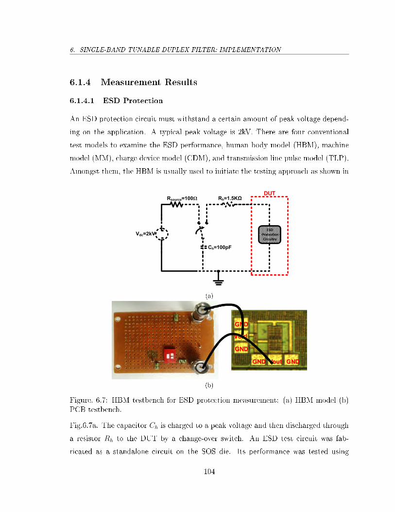
6. SINGLE-BAND TUNABLE DUPLEX FILTER: IMPLEMENTATION
6.1.4 Measurement Results
6.1.4.1 ESD Protection
An ESD protection circuit must withstand a certain amount of peak voltage depend-
ing on the application. A typical peak voltage is 2kV. There are four conventional
test models to examine the ESD performance, human body model (HBM), machine
model (MM), charge device model (CDM), and transmission line pulse model (TLP).
Amongst them, the HBM is usually used to initiate the testing approach as shown in
DCVdc=2kV
Rsource=100Ω Rh=1.5KΩ
Ch=100pF
DUT
ESD Protection
Circuitry
(a)
(b)
Figure. 6.7: HBM testbench for ESD protection measurement: (a) HBM model (b)PCB testbench.
Fig.6.7a. The capacitor Ch is charged to a peak voltage and then discharged through
a resistor Rh to the DUT by a change-over switch. An ESD test circuit was fab-
ricated as a standalone circuit on the SOS die. Its performance was tested using
104

6. SINGLE-BAND TUNABLE DUPLEX FILTER: IMPLEMENTATION
a HBM built on a dot matrix board (Fig.6.7b). Connections to the chip were via
a CASCADE probe station (not shown). Charging the Ch to a large voltage was
not practical in the lab, thus, the capacitor was only charged to 30V. Two possible
ESD strikes as well as a ramp voltage were generated and the measured results show
that the ESD output voltage does not exceed ±4V under any of these circumstances
(Fig.6.8).
(a) (b)
(c)
Figure. 6.8: Measurement results of the output voltage of the ESD protection circuitfor an input: (a) positive ESD strike (b) negative ESD strike (c) ramp voltage up to30V.
105

6. SINGLE-BAND TUNABLE DUPLEX FILTER: IMPLEMENTATION
6.1.4.2 Tunable Duplex Filter
The fabricated duplex lter chip has an active area including ESD protections and
pads of 2.42mm2. Fig.6.9 shows the micro-photograph of the chip. The die was
Figure. 6.9: Die micro-photograph of the duplex lter.
directly measured by CASCADE GSG RF micro-probes for three RF pads, and a
multi-nger DC probe supplied the required control voltages for the DSCB's. Since
the DSCB requires a negative voltage to turn o the FET switches, a PCB was
designed to provide adjustable bipolar control voltages to cover all possible 64 states
of the DSCB (Fig.6.10).
Fig.6.11a illustrates the measured Tx to Rx isolation with Tx powers up to 28dBm.
The measured null frequencies are approximately 10% below the post-layout simu-
lation results, with the lower null shifting more than the upper null producing an
unwanted increase in the frequency oset. However, the critical Tx isolation of 19dB
and Rx isolation of 13-14dB at the specied fd = 190MHz are close to simulations.
106
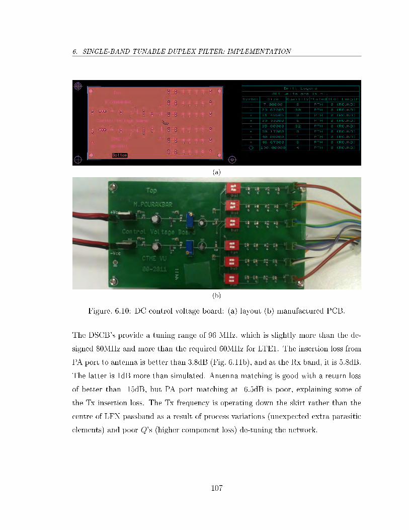
6. SINGLE-BAND TUNABLE DUPLEX FILTER: IMPLEMENTATION
(a)
(b)
Figure. 6.10: DC control voltage board: (a) layout (b) manufactured PCB.
The DSCB's provide a tuning range of 96 MHz, which is slightly more than the de-
signed 80MHz and more than the required 60MHz for LTE1. The insertion loss from
PA port to antenna is better than 3.8dB (Fig. 6.11b), and at the Rx band, it is 5.8dB.
The latter is 1dB more than simulated. Antenna matching is good with a return loss
of better than -15dB, but PA port matching at -6.5dB is poor, explaining some of
the Tx insertion loss. The Tx frequency is operating down the skirt rather than the
centre of LFN passband as a result of process variations (unexpected extra parasitic
elements) and poor Q's (higher component loss) de-tuning the network.
107

6. SINGLE-BAND TUNABLE DUPLEX FILTER: IMPLEMENTATION
-25
-20
-15
-10
-5
0
1.6 1.8 2.0 2.2 2.4
|S1
3|
(dB
)
Frequency (GHz)
000 001010 011100 101110 111
(a)
-40
-35
-30
-25
-20
-15
-10
-5
0
-40
-35
-30
-25
-20
-15
-10
-5
0
1.6 1.8 2.0 2.2 2.4
|S22
| (dB
)
|S21
| (dB
)
Frequency (GHz)
IL(TX) 000IL(TX) 111RL(ANT) 000RL(ANT) 111
TX-to-ANT
ANT PORT
(b)
Figure. 6.11: Measured frequency response: (a) Tx-to-Rx isolation for dierent DSCBsettings (b) Tx insertion loss and the return loss at antenna port for two major states(000-111).
A post-measurement study shown in Fig. 6.12 varied the inductance Q in the
post-layout simulation. It indicated that an inductor with a minimum Q of 43 results
108
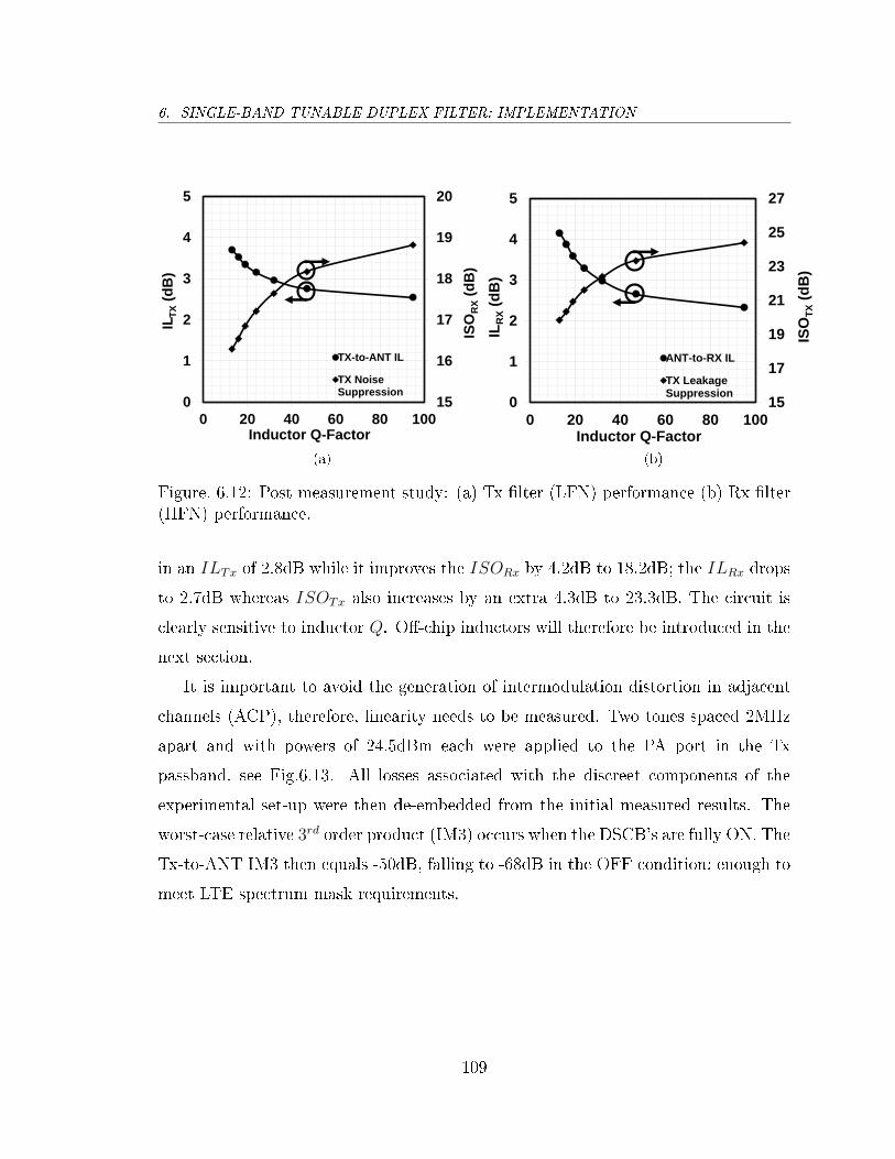
6. SINGLE-BAND TUNABLE DUPLEX FILTER: IMPLEMENTATION
15
16
17
18
19
20
0
1
2
3
4
5
0 20 40 60 80 100
ILT
X (
dB
)
Inductor Q-Factor
TX-to-ANT IL
TX NoiseSuppression
ISO
RX (
dB
) (a)
15
17
19
21
23
25
27
0
1
2
3
4
5
0 20 40 60 80 100
ILR
X (
dB
)
Inductor Q-Factor
ANT-to-RX IL
TX LeakageSuppression
ISO
TX (
dB
)
(b)
Figure. 6.12: Post-measurement study: (a) Tx lter (LFN) performance (b) Rx lter(HFN) performance.
in an ILTx of 2.8dB while it improves the ISORx by 4.2dB to 18.2dB; the ILRx drops
to 2.7dB whereas ISOTx also increases by an extra 4.3dB to 23.3dB. The circuit is
clearly sensitive to inductor Q. O-chip inductors will therefore be introduced in the
next section.
It is important to avoid the generation of intermodulation distortion in adjacent
channels (ACP), therefore, linearity needs to be measured. Two tones spaced 2MHz
apart and with powers of 24.5dBm each were applied to the PA port in the Tx
passband, see Fig.6.13. All losses associated with the discreet components of the
experimental set-up were then de-embedded from the initial measured results. The
worst-case relative 3rd order product (IM3) occurs when the DSCB's are fully ON. The
Tx-to-ANT IM3 then equals -50dB, falling to -68dB in the OFF condition; enough to
meet LTE spectrum mask requirements.
109

6. SINGLE-BAND TUNABLE DUPLEX FILTER: IMPLEMENTATION
PA
COMBINER/SPILITER
CIRCULATOR
50 Ω PA
CIRCULATOR
50 Ω
ATTENUATOR20dB
CIRCULATOR
50 Ω
POWER SUPPLY
OUTPUT 2OUTPUT 1
DC CONTROL VOLTAGE BOARD
POSITIVE VOLTAGE
NEGATIVE VOLTAGE
AC
P RF PR
OB
E TX
G
G
S
ACP RF PROBE ANTENNA
G S G
COUPLER
GGB MULTI-WEDGES DC PROBE
VCT3 VCT2 VCT1 VCR3 VCR2 VCR1G G G G
ATTENUATOR10dB
ATTENUATOR6dB
ATTENUATOR10dB
ATTENUATOR6dB
S
G
G
AC
P R
F PR
OB
E
R
X
RF ASIC
SIGNAL GENERATOR
RF OUT
FREQUENCY MHz
POWER dBm
SPECTRUM ANALYZER
RF INPUT
SPECTRUM ANALYZER
RF INPUT
SPECTRUM ANALYZER
RF INPUTSIGNAL GENERATOR
RF OUT
FREQUENCY MHz
POWER dBm
(a)
(b)
Figure. 6.13: Measurement set-up for the IMDs analysis: (a) building blocks (b)experimental set-up.
110

6. SINGLE-BAND TUNABLE DUPLEX FILTER: IMPLEMENTATION
PA
ATTENUATOR20dB
POWER SUPPLY
OUTPUT 2OUTPUT 1
DC CONTROL VOLTAGE BOARD
POSITIVE VOLTAGE
NEGATIVE VOLTAGE
AC
P RF PR
OB
E TX
G
G
S
ACP RF PROBE ANTENNA
G S G
COUPLER
GGB MULTI-WEDGES DC PROBE
VCT3 VCT2 VCT1 VCR3 VCR2 VCR1G G G G
ATTENUATOR10dB
ATTENUATOR6dB
S
G
G
AC
P R
F PR
OB
E
R
X
RF ASICDIE
ATTENUATOR10dB
ATTENUATOR6dB
SPECTRUM ANALYZER
RF INPUT
SPECTRUM ANALYZER
RF INPUT
SPECTRUM ANALYZER
RF INPUT
SIGNAL GENERATOR
RF OUT
FREQUENCY MHz
POWER dBm
Figure. 6.14: Measurement set-up for the P1dB analysis.
Fig.6.14 shows the experimental set-up to obtain the P1dB points when the DSCB's
are fully OFF (000) and fully ON (111). The measured results indicate that both
lters have relatively linear response until the input power hits to 27dBm, see Fig.6.15.
However, measurements at higher power are not valid since the output power starts to
expand due to the compression of the spectrum analyser measuring the input signal
power.
111

6. SINGLE-BAND TUNABLE DUPLEX FILTER: IMPLEMENTATION
(a) (b)
(c) (d)
Figure. 6.15: Measured compression behaviour of the lters for Tx-to-Ant (a) Txupper band edge (000) (b) Tx lower band edge (111), and for Ant-to-Rx (c) Rx upperband edge (000) (d) Rx lower band edge (111).
6.2 PCB Duplex Filters: Proof of Concept
The previous section indicates the need for high-Q inductors.This section describes a
PCB variant with high-Q components. The switches and capacitors are commercial
o-the-shelf products. Due to voltage limitations on the switches, the 'dual' LFN lter
topology described in Chapter 4 is employed. This addresses the large peak voltage
112

6. SINGLE-BAND TUNABLE DUPLEX FILTER: IMPLEMENTATION
issue associated with its counterpart. The structure has a lower peak voltage, however,
the circuit experiences a higher peak current at resonance. The post-measurement
study in the previous section indicates that the inductor Q-factor must be increased.
Since on-chip inductors have a relatively low-Q, a high-Q PCB inductor was fabricated
on a four-layer FR4 substrate as depicted in Fig. 6.16. In order to obtain a high Q,
all the metallizations underneath the inductor loop were etched away. After SOLT
(Short-Open-Load-Thru) de-embedding, the measured inductance and Q at 2GHz
was 1.19nH and 125, respectively.
FR4 Core
FR4 Prepreg
FR4 Prepreg
AIR
AIR
CU CU
CU CU
CU CU
CU CU1oz. 1oz.
150µm
150µm
380µm
(a) (b)
Geometrical Data
Parameter InductorWidth/Spacing 0.5 mm /0.389 mmOuter Diameter 1.490 mmInd. Length 2.723 mm
De-embedded Interco. Length 5.37 mm
(c)
Figure. 6.16: Laminated inductor: (a) Cross-section (b) layout from bottom: DUT,Short, Open, Thru, Load (c) Geometry.
113
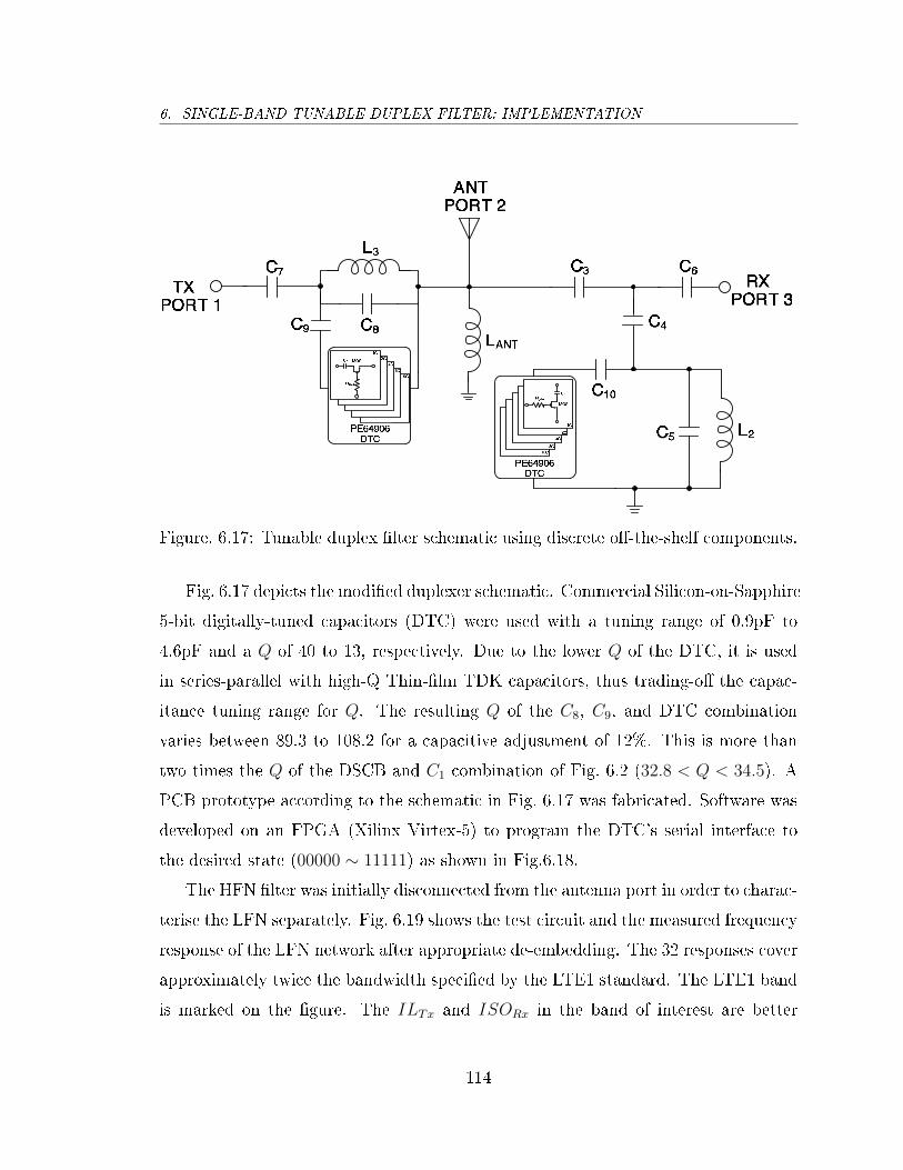
6. SINGLE-BAND TUNABLE DUPLEX FILTER: IMPLEMENTATION
Figure. 6.17: Tunable duplex lter schematic using discrete o-the-shelf components.
Fig. 6.17 depicts the modied duplexer schematic. Commercial Silicon-on-Sapphire
5-bit digitally-tuned capacitors (DTC) were used with a tuning range of 0.9pF to
4.6pF and a Q of 40 to 13, respectively. Due to the lower Q of the DTC, it is used
in series-parallel with high-Q Thin-lm TDK capacitors, thus trading-o the capac-
itance tuning range for Q. The resulting Q of the C8, C9, and DTC combination
varies between 89.3 to 108.2 for a capacitive adjustment of 12%. This is more than
two times the Q of the DSCB and C1 combination of Fig. 6.2 (32.8 < Q < 34.5). A
PCB prototype according to the schematic in Fig. 6.17 was fabricated. Software was
developed on an FPGA (Xilinx Virtex-5) to program the DTC's serial interface to
the desired state (00000 ∼ 11111) as shown in Fig.6.18.
The HFN lter was initially disconnected from the antenna port in order to charac-
terise the LFN separately. Fig. 6.19 shows the test circuit and the measured frequency
response of the LFN network after appropriate de-embedding. The 32 responses cover
approximately twice the bandwidth specied by the LTE1 standard. The LTE1 band
is marked on the gure. The ILTx and ISORx in the band of interest are better
114

6. SINGLE-BAND TUNABLE DUPLEX FILTER: IMPLEMENTATION
Figure. 6.18: FPGA Virtex-5 interface with a high-speed VHDC port and real-timedisplay of decimal DTC state.
(a)
1.8 1.9 2 2.1 2.2 2.3−40
−35
−30
−25
−20
−15
−10
−5
0
|S21
| (d
B)
Frequency (GHz)
Measured TX−to−ANT (S21
)
RXBand
TXBand
(b)
Figure. 6.19: The LFN lter: (a) Top:FPGA interface. Bot LHS:PCB. BotRHS:SOLT calibration-kit (b) measured frequency response for 32 DTC settings.
115

6. SINGLE-BAND TUNABLE DUPLEX FILTER: IMPLEMENTATION
than 3.3dB and 26dB, respectively. The frequency response curves between the thick
highlighted traces provide optimum ISO performance, (but not optimum IL). It is
possible to trade-o isolation and insertion loss by not selecting the exact null position
and operating on the null skirt. Moving the left hand boundary four traces to the
right reduces isolation to 23.5dB (still better thatn the 20dB target) but improves IL
to 2.9dB.
Figure. 6.20: Measurement set-up for PCB duplex lter: Bot LHS: PCB. Bot RHS:SOLT calibration-kit.
The complete tunable duplex lter was then measured (see Fig.6.20) with results
shown in Fig. 6.21. The isolation is better than 25dB at Tx and 31dB at Rx frequen-
cies, an improvement of 7dB and 18dB, respectively on the fully integrated circuit.
EM-simulations predicted 10dB and 14 dB improvements. Worst-case Tx and Rx
insertion loss is 3.6dB and 3.7dB, an improvement of 0.2dB and 2.1dB respectively.
A lower than predicted 1.1dB improvement in ILTx occurs at one end of the band
only and is due to a combination of passband frequency shift (see section 4.2) and the
predicted fd variation which could be compensated by making C7 and C4 tunable.
116
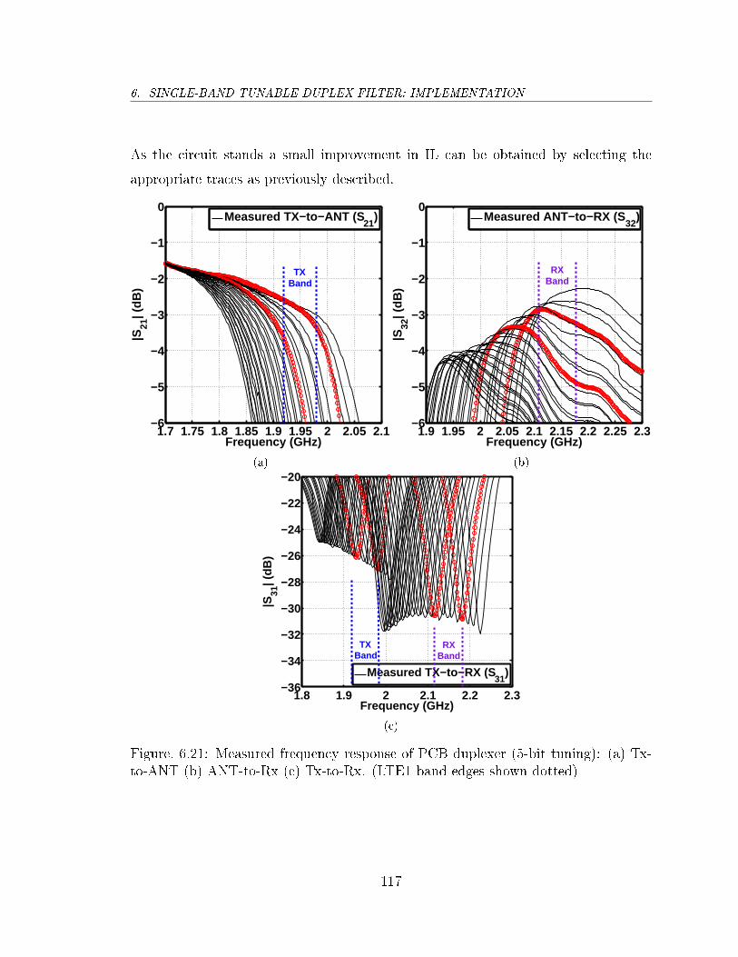
6. SINGLE-BAND TUNABLE DUPLEX FILTER: IMPLEMENTATION
As the circuit stands a small improvement in IL can be obtained by selecting the
appropriate traces as previously described.
1.7 1.75 1.8 1.85 1.9 1.95 2 2.05 2.1−6
−5
−4
−3
−2
−1
0
|S21
| (d
B)
Frequency (GHz)
Measured TX−to−ANT (S21
)
TXBand
(a)
1.9 1.95 2 2.05 2.1 2.15 2.2 2.25 2.3−6
−5
−4
−3
−2
−1
0
|S32
| (d
B)
Frequency (GHz)
Measured ANT−to−RX (S32
)
RXBand
(b)
1.8 1.9 2 2.1 2.2 2.3−36
−34
−32
−30
−28
−26
−24
−22
−20
|S31
| (d
B)
Frequency (GHz)
Measured TX−to−RX (S31
)
RX Band
TX Band
(c)
Figure. 6.21: Measured frequency response of PCB duplexer (5-bit tuning): (a) Tx-to-ANT (b) ANT-to-Rx (c) Tx-to-Rx. (LTE1 band edges shown dotted)
117
6. SINGLE-BAND TUNABLE DUPLEX FILTER: IMPLEMENTATION
6.3 Summary
This chapter contains two implementations on the single-band tunable duplex lters
for the LID. The fully integrated solution was developed on the SOS process. The
obtained isolation is 19dB and 13-14dB for ISOTx and ISORx, respectively. It is
close to the minimum specication of 15dB for the LID. However, the insertion loss
is still not competitive with the existing duplexers.
The o-the-shelf solution with PCB high-Q inductors improved the isolation per-
formance to well above 20dB for both bands and reduced the insertion loss to 3.6dB
and 3.7dB for ILTx and ILRx, respectively. These results are within 1dB and 0.5dB
for the commercial SAW/BAW duplexers (Table 3.1). Further improvement is still
necessary and can be addressed by improving the DTC using a combination of cus-
tom designs and modern SOI technologies with lower FOM. A recent announcement
indicates three times improvement in FOM is now available [81].
The next chapter considers a multi-band solution by expanding the tuning range
and controlling the duplex oset.
118

Chapter 7
Multi-band Tunable Duplex Filters:
Simulation
High-Q passives are essential to increase the isolation and reduce the insertion loss of
the LID. On the other hand, more tunable capacitors are needed to tune the structure
to dierent LTE bands with dierent duplex osets (Chapter 4). The previous chapter
demonstrated high-Q inductors can be fabricated on laminates with small footprints.
Therefore, multiple DSCBs connected to high-Q laminate inductors via interconnects
is a potential solution to the LID problem.
Wire-bond, solder ball, and copper pillar are generally utilised as chip-to-substrate
interconnects. In this chapter, the impact of these joints on the achievable quality
factor of a planar inductor is investigated. Each joint is mathematically analysed using
a simple pi-model in Section 7.1. Results show good agreement between model and
EM-simulation results (within 10%). Two multi-band LTE duplex lter prototypes
are presented in Section 7.2 and Section 7.3. The work in Section 7.2 was completed
while on an internship at Ericsson and Lund University, Sweden where access to the
SOI process and fabrication was provided. A summary concludes in Section 7.4.
119

7. MULTI-BAND TUNABLE DUPLEX FILTERS: SIMULATION
7.1 Die-to-Substrate Interconnects for High-Q PCB
Inductors
Inductors have a direct impact on the duplex lters circuit performance. Since the
silicon inductors possess a low quality factor, high-Q inductors can be realised either
by discrete surface mount devices or by ceramic or organic substrates. Wire-bonding
or ip-chip processing are common integration methods. These processes aect the
overall performance by adding extra parasitic elements to the nominal value of the
inductor [82]. This section addresses the impact of chip-to-substrate interconnections
on high-Q inductors in organic substrates.
7.1.1 Chip-to-Substrate Interconnections
7.1.1.1 Wire-bond Connection Model
The wire bonding process generally uses gold (Au) or aluminium (Al) wires due to
their high electrical conductivity and resistance to oxidation. However, the bond wire
and its large pad size introduces parasitics that substantially degrade the electrical
characteristics of the designed circuit at GHz frequencies. Thus, it is necessary that
the electrical parameters of the wire-bond be extracted and modelled properly. A
wire bond trace is normally characterised by its inductance (LWB), series resistance
(RWB), and the parasitic capacitance (CWB) to the ground of the substrate. Fig. 7.1
shows the layout and the equivalent scalable π-model of a wire-bond. The inductance
is mainly dominated by length (l) and radius (r) of the wire, and can be approximated
as
LWB 'µl
2π(ln(
2l
r− 0.75)) (7.1)
where µ is the permeability in free space. At frequencies in the GHz region, the
skin and proximity eects become severe resulting in the series resistance of the wire
bond being frequency dependent. In order to accurately model the skin eect, the
120

7. MULTI-BAND TUNABLE DUPLEX FILTERS: SIMULATION
skin depth (δ ' 0.075√f) and the conductivity (σ) of the material must be considered.
Therefore, RWB can be estimated by
RWB 'l
πr2σ+
l
2πrδσ(7.2)
The parasitic capacitance between the wire-bond and the substrate ground (CWB)
can be estimated as follows [83]
CWB '2πεl
arctan(dr)
(7.3)
where ε and d are the permittivity, and the distance between the centre of the wire-
bond and the substrate ground metallisations, respectively. It should be noted that
the eect of fringing capacitances is neglected in order to simplify the total capacitance
expression.
(a)
WB
WB WB
WB
(b)
Figure. 7.1: Wire-bond Interconnection: (a) 3D structure of a wire-bond (b) Equiva-lent circuit of a wire-bond.
7.1.1.2 Flip-chip Connection Model
A ip-chip solution oers several bumping options including solder ball, gold stud
bump, micro bump, and copper pillar [84]. Among these type of connections, the
solder and copper pillar bumps are normally used due to their low cost, short elec-
trical connection length, and high reliability. A ip-chip contact is generally formed
121

7. MULTI-BAND TUNABLE DUPLEX FILTERS: SIMULATION
by a ball of solder paste (SB), or a copper pillar (CP ), as shown in Fig. 7.2. Flip-
chip contacts can be modelled as a transmission line. Considering the structure of a
circular cylinder, the transition signal from die to the board is aected by the para-
sitic elements of the connections which are self-inductance (LSB &LCP ), capacitance
(CSB &CCP ), and resistance (RSB &RCP ) of the bump. For operating frequencies in
the GHz region, the impact of these parasitic eects becomes severe. The Pi-model
can be used to predict the behaviour of the ip-chip connections. A scalable model of
a bump and a copper pillar is illustrated in Fig. 7.3. The inductance of the ip-chip
connection is proportional to the bump height, radius, and overlap of the top and
bottom pads. The self-inductance of a cylindrical bump is given by [85]
LSB &CP =µh
2π[lnh
a+
√(1 +
h2
a2)−
√(1 +
a2
h2) +
a
h] (7.4)
where a is the bump radius and h is the bump height. By taking the skin eect into
account, the resistance of the bump can also be estimated as follows
RSB &CP '√µπσf
σπah (7.5)
The parasitic capacitance from the ip-chip to the substrate, or chip ground metalli-
sation, is also given by
CSB = 4πεa CCP =2πεh
ln(1 + da)
(7.6)
where ε is the relative permittivity of the dielectric; and d is the distance between
the copper pillar and the substrate/chip ground. Simulations using Matlab and ADS
Momentum were used to verify the accuracy of the models. Scattering parameters
were extracted by the EM-simulator and the admittance matrix generated. The series
inductance, series resistance, and shunt capacitance, of the model are computed.
Table 7.1 summarises the values of the model elements at frequency of 2GHz for
122
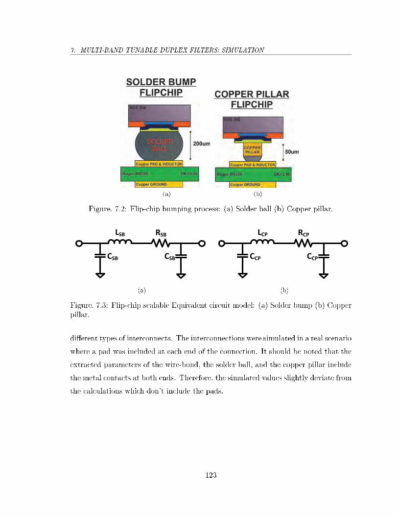
7. MULTI-BAND TUNABLE DUPLEX FILTERS: SIMULATION
(a) (b)
Figure. 7.2: Flip-chip bumping process: (a) Solder ball (b) Copper pillar.
CSB
LSB RSB
CSB
(a)
CCP
LCP RCP
CCP
(b)
Figure. 7.3: Flip-chip scalable Equivalent circuit model: (a) Solder bump (b) Copperpillar.
dierent types of interconnects. The interconnections were simulated in a real scenario
where a pad was included at each end of the connection. It should be noted that the
extracted parameters of the wire-bond, the solder ball, and the copper pillar include
the metal contacts at both ends. Therefore, the simulated values slightly deviate from
the calculations which don't include the pads.
123

7. MULTI-BAND TUNABLE DUPLEX FILTERS: SIMULATION
Table 7.1: Summary of Interconnect Modelling Parameters
Equivalent Circuit Parameters
Method Leff (pH) Rseries(mΩ) Cshunt(fF )Cal. Sim. Cal. Sim. Cal. Sim.
Wire-Bond 1005 1031 326 437 20.37 35Solder Bump 50.82 56.46 34.04 31.95 10.84 6.87Copper Pillar 25.41 26.44 23.03 24.52 7.33 8.72
7.1.2 Planar Laminate Inductor Design
7.1.2.1 Theoretical Consideration
Planar inductors are commonly used in most radio frequency integrated circuits
(RFICs). Their performance is generally assessed by the eective inductance per
unit area (Leff ), the quality factor (Q), self-resonance frequency (fres), and maxi-
mum current rating. Depending on design requirements, several other temperature
dependent parameters should be considered. Inductors are often constructed in dif-
ferent geometric shapes such as rectangular, square or circular spiral, meander, and
simple stub lines. The Leff depends on the inductor geometry and consists of two
components given by
Leff = Ls ±M (7.7)
where Ls is self-inductance, and M is mutual inductance. Ls is dominated by the
conductor trace length (l), width (W ), and thickness (t), while M is caused by the
coupling between the adjacent conductor tracks. The mutual inductance can be either
positive, where the current vectors are in the same direction, or negative if the current
vectors are in opposite directions. The meander inductor is a good example of a design
with negative M as the current ows as shown in Fig. 7.4. Therefore, this particular
shape has a lower inductance compared to a spiral inductor with the same area. In
order to calculate the Leff of an arbitrary shape, [86] introduced an expression based
on current sheet approximation that applies the concepts of geometry mean distance
124
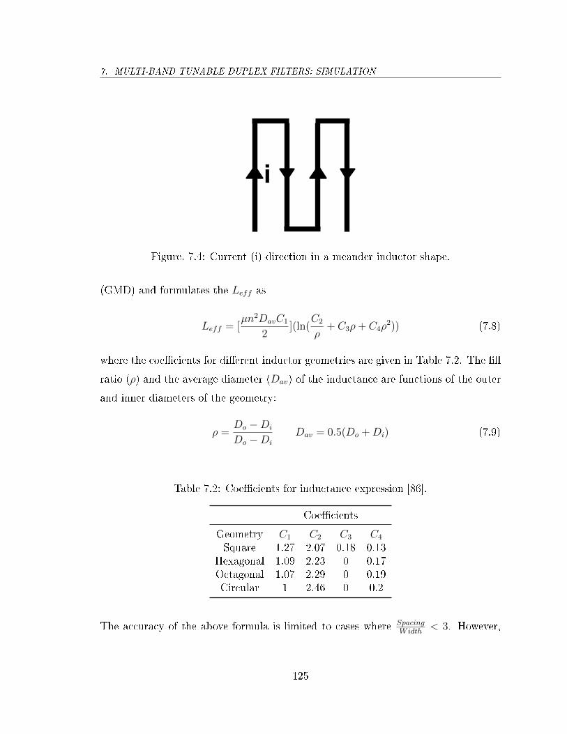
7. MULTI-BAND TUNABLE DUPLEX FILTERS: SIMULATION
Figure. 7.4: Current (i) direction in a meander inductor shape.
(GMD) and formulates the Leff as
Leff = [µn2DavC1
2](ln(
C2
ρ+ C3ρ+ C4ρ
2)) (7.8)
where the coecients for dierent inductor geometries are given in Table 7.2. The ll
ratio (ρ) and the average diameter (Dav) of the inductance are functions of the outer
and inner diameters of the geometry:
ρ =Do −Di
Do −Di
Dav = 0.5(Do +Di) (7.9)
Table 7.2: Coecients for inductance expression [86].
Coecients
Geometry C1 C2 C3 C4
Square 1.27 2.07 0.18 0.13Hexagonal 1.09 2.23 0 0.17Octagonal 1.07 2.29 0 0.19Circular 1 2.46 0 0.2
The accuracy of the above formula is limited to cases where SpacingWidth
< 3. However,
125

7. MULTI-BAND TUNABLE DUPLEX FILTERS: SIMULATION
practical inductors can be designed with a smaller spacing that improves the inter-
winding magnetic coupling as well as reducing the inductor footprint. Leff is depen-
dent on the inductor shape. Fig. 7.5 compares dierent shapes with the same track
width, spacing, and various number of turns. Increasing n adds additional conductor
trace length translating to higher Leff and also lower fres. Equation (7.8) gives a
good initial prediction for the required n. Generally, the Leff is more dependent on
geometry than sheet resistance and conductor trace width. The Q-factor is closely
1 1.5 2 2.5 3 3.5 40
2
4
6
8
10
12
14
16
18
20
Number of Turns (n)
Effe
ctiv
e In
duct
ance
(nH
)
SquareHexagonalOctagonalCircular
Figure. 7.5: Eective inductance value for dierent inductance geometries (Do =1.5mm).
coupled to the loss mechanisms in a planar inductor, which are mainly dominated by
parasitic resistance and capacitance. In other words, the eddy current, skin eect, and
proximity, limit the achievable Q-factor. At DC and low frequencies, the Q-factor
is determined by the series resistance of the conductor turns. At RF frequencies,
current cannot deeply ow into the conductor trace due to the skin eect, therefore,
126
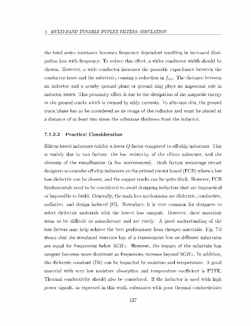
7. MULTI-BAND TUNABLE DUPLEX FILTERS: SIMULATION
the total series resistance becomes frequency dependent resulting in increased dissi-
pation loss with frequency. To reduce this eect, a wider conductor width should be
chosen. However, a wide conductor increases the parasitic capacitance between the
conductor trace and the substrate, causing a reduction in fres. The distance between
an inductor and a nearby ground plane or ground ring plays an important role in
inductor losses. This proximity eect is due to the dissipation of the magnetic energy
in the ground tracks which is created by eddy currents. To alleviate this, the ground
trace/plane has to be considered as an image of the inductor and must be placed at
a distance of at least two times the substrate thickness from the inductor.
7.1.2.2 Practical Consideration
Silicon-based inductors exhibit a lower Q-factor compared to o-chip inductors. This
is mainly due to two factors: the low resistivity of the silicon substrate, and the
thinness of the metallisation (a few micrometres). Both factors encourage circuit
designers to consider o-chip inductors on the printed circuit board (PCB) where a low
loss dielectric can be chosen, and the copper tracks can be quite thick. However, PCB
fundamentals need to be considered to avoid designing inductors that are impractical
or impossible to build. Generally, the main loss mechanisms are dielectric, conductive,
radiative, and design induced [87]. Nowadays, it is very common for designers to
select dielectric materials with the lowest loss tangent. However, these materials
seem to be dicult to manufacture and are costly. A good understanding of the
loss factors may help achieve the best performance from cheaper materials. Fig. 7.6
shows that the simulated insertion loss of a transmission line on dierent substrates
are equal for frequencies below 3GHz. However, the impact of the substrate loss
tangent becomes more dominant as frequencies increase beyond 9GHz. In addition,
the dielectric constant (Dk) can be impacted by moisture and temperature. A good
material with very low moisture absorption and temperature coecient is PTFE.
Thermal conductivity should also be considered. If the inductor is used with high
power signals, as expected in this work, substrates with poor thermal conductivities
127

7. MULTI-BAND TUNABLE DUPLEX FILTERS: SIMULATION
will degrade the overall performance. For this reason PTFE was not chosen for the
LID. Roger core material of R4350 has better thermal conductivity compared to the
FR4, therefore, it was chosen here.
( H ) sc yc
qIucc6
q)ucc6
qzucc6
qHucc6
qGucc6
q(ucc6
qyucc6
qsucc6
cuccc
653
6653
Figure. 7.6: Insertion Loss of a transmission line simulated on dierent laminatematerials.
The conductor loss is proportional to the resistance of the metal trace, therefore
the surface nish is very crucial due to the skin eect phenomena. A smooth nish
would substantially decrease the loss.
Transmission lines are widely used in PCBs and are a source of radiation loss.
Generally, microstrip traces on the outer layers of the PCB radiate more energy,
than striplines on the inner layers. Also, discontinuities in the signal traces cause
improper transitions (matching) between dierent transmission lines. Other PCB
design factors such as, a practical PCB stack-up, proper selection of the via type, and
process tolerance specication can aect the quality factor of the inductor.
128
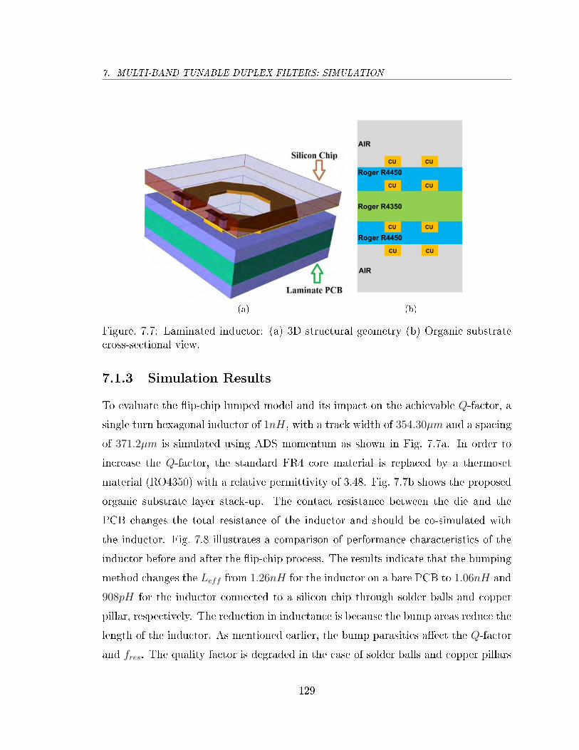
7. MULTI-BAND TUNABLE DUPLEX FILTERS: SIMULATION
(a) (b)
Figure. 7.7: Laminated inductor: (a) 3D structural geometry (b) Organic substratecross-sectional view.
7.1.3 Simulation Results
To evaluate the ip-chip lumped model and its impact on the achievable Q-factor, a
single turn hexagonal inductor of 1nH, with a track width of 354.30µm and a spacing
of 371.2µm is simulated using ADS momentum as shown in Fig. 7.7a. In order to
increase the Q-factor, the standard FR4 core material is replaced by a thermoset
material (RO4350) with a relative permittivity of 3.48. Fig. 7.7b shows the proposed
organic substrate layer stack-up. The contact resistance between the die and the
PCB changes the total resistance of the inductor and should be co-simulated with
the inductor. Fig. 7.8 illustrates a comparison of performance characteristics of the
inductor before and after the ip-chip process. The results indicate that the bumping
method changes the Leff from 1.26nH for the inductor on a bare PCB to 1.06nH and
908pH for the inductor connected to a silicon chip through solder balls and copper
pillar, respectively. The reduction in inductance is because the bump areas reduce the
length of the inductor. As mentioned earlier, the bump parasitics aect the Q-factor
and fres. The quality factor is degraded in the case of solder balls and copper pillars
129

7. MULTI-BAND TUNABLE DUPLEX FILTERS: SIMULATION
H ) f i G(( GH
cG(y
cEy(
(y((
Ey(
G(y
cGEy
GEy
6Fr
6 6Fr
(a)
G z Q l (yy (G
Hynyy6
Qynyy6
iynyy6
(Gyny6
()yny6
(lyny6
ynyyyy
Gyyny6
65F
6
(b)
Figure. 7.8: EM-simulation results of a laminated inductor with dierent intercon-nections: (a) Eective inductance (Leff ) (b) Q-factor.
by 35% and 38.7%, respectively. Additionally, both cases reduce the fres as shown in
Fig. 7.8a. For our LID application, solder bumps are preferred. They have slightly
better performance and lower manufacturing cost. Copper pillars lead to a higher
density of interconnects with a smaller pitch which is not required for the LID.
7.2 Quad-band SOI Duplex Filter
The previous chapter described two solutions for the single-band LID. This section
is devoted to an integrated SOI solution of the multi-band low-isolation device using
the ST Microelectronics 130nm process. A passive ltering approach, relying on
small footprint inductance and capacitance elements is used. Since silicon inductors
are generally low Q, high-Q PCB inductors are employed. We choose a ip-chip
integration approach that provides low-ohmic contacts between the silicon die and
the PCB.
130

7. MULTI-BAND TUNABLE DUPLEX FILTERS: SIMULATION
L1
Figure. 7.9: Multi-band tunable SOI duplex lter.
The low-isolation device was designed to cover LTE band 1,2,3, and 7, for which
the duplex distance is 190MHz, 80MHz, 95MHz, and 120MHz, respectively (Table 7.3).
Fig. 7.9 shows the schematic of the combined LFN and HFN lters. A 130nm Silicon-
on-Insulator (SOI) process was chosen due to its lower FOM of 280fs. The LTE UE
transmitter power (class 3) is currently specied at 23dBm ± 2dBm. Since no DC
current ows through the duplex lters, SOI passive components can easily tolerate
such a power. A number of FET devices are stacked to accommodate the power level.
131
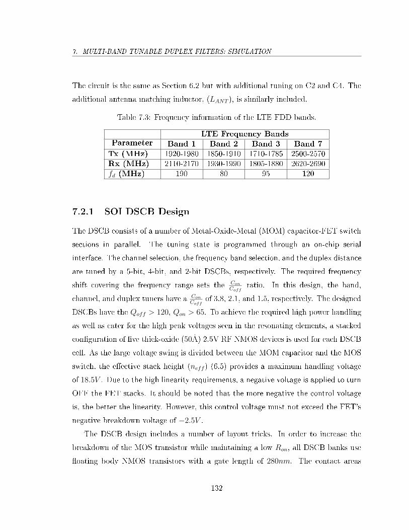
7. MULTI-BAND TUNABLE DUPLEX FILTERS: SIMULATION
The circuit is the same as Section 6.2 but with additional tuning on C2 and C4. The
additional antenna matching inductor, (LANT ), is similarly included.
Table 7.3: Frequency information of the LTE FDD bands.
ParameterLTE Frequency Bands
Band 1 Band 2 Band 3 Band 7Tx (MHz) 1920-1980 1850-1910 1710-1785 2500-2570Rx (MHz) 2110-2170 1930-1990 1805-1880 2620-2690fd (MHz) 190 80 95 120
7.2.1 SOI DSCB Design
The DSCB consists of a number of Metal-Oxide-Metal (MOM) capacitor-FET switch
sections in parallel. The tuning state is programmed through an on-chip serial
interface. The channel selection, the frequency band selection, and the duplex distance
are tuned by a 5-bit, 4-bit, and 2-bit DSCBs, respectively. The required frequency
shift covering the frequency range sets the Con
Coffratio. In this design, the band,
channel, and duplex tuners have a Con
Coffof 3.8, 2.1, and 1.5, respectively. The designed
DSCBs have the Qoff > 120, Qon > 65. To achieve the required high power handling
as well as cater for the high peak voltages seen in the resonating elements, a stacked
conguration of ve thick-oxide (50Å) 2.5V RF NMOS devices is used for each DSCB
cell. As the large voltage swing is divided between the MOM capacitor and the MOS
switch, the eective stack height (neff ) (6.5) provides a maximum handling voltage
of 18.5V . Due to the high linearity requirements, a negative voltage is applied to turn
OFF the FET stacks. It should be noted that the more negative the control voltage
is, the better the linearity. However, this control voltage must not exceed the FET's
negative breakdown voltage of −2.5V .
The DSCB design includes a number of layout tricks. In order to increase the
breakdown of the MOS transistor while maintaining a low Ron, all DSCB banks use
oating body NMOS transistors with a gate length of 280nm. The contact areas
132
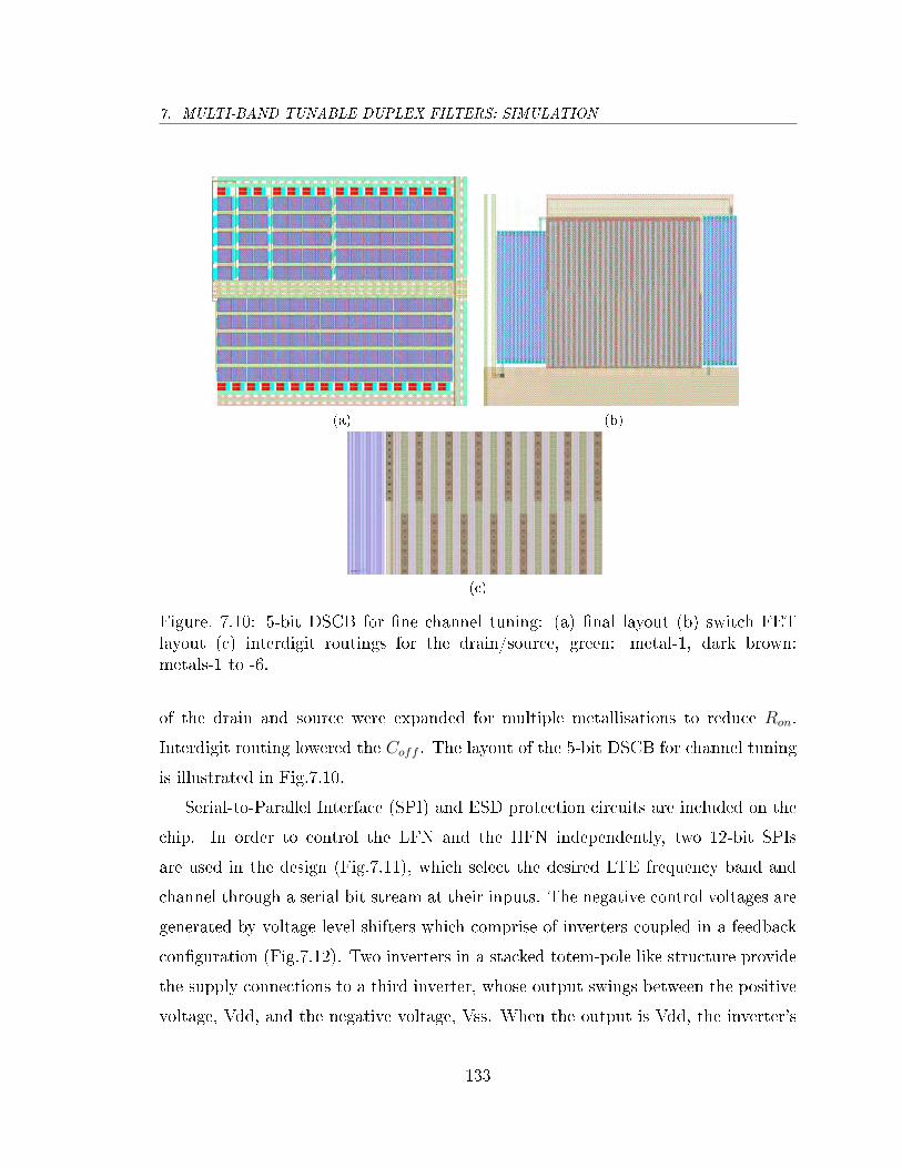
7. MULTI-BAND TUNABLE DUPLEX FILTERS: SIMULATION
(a) (b)
(c)
Figure. 7.10: 5-bit DSCB for ne channel tuning: (a) nal layout (b) switch FETlayout (c) interdigit routings for the drain/source, green: metal-1, dark brown:metals-1 to -6.
of the drain and source were expanded for multiple metallisations to reduce Ron.
Interdigit routing lowered the Coff . The layout of the 5-bit DSCB for channel tuning
is illustrated in Fig.7.10.
Serial-to-Parallel Interface (SPI) and ESD protection circuits are included on the
chip. In order to control the LFN and the HFN independently, two 12-bit SPIs
are used in the design (Fig.7.11), which select the desired LTE frequency band and
channel through a serial bit stream at their inputs. The negative control voltages are
generated by voltage level shifters which comprise of inverters coupled in a feedback
conguration (Fig.7.12). Two inverters in a stacked totem-pole like structure provide
the supply connections to a third inverter, whose output swings between the positive
voltage, Vdd, and the negative voltage, Vss. When the output is Vdd, the inverter's
133
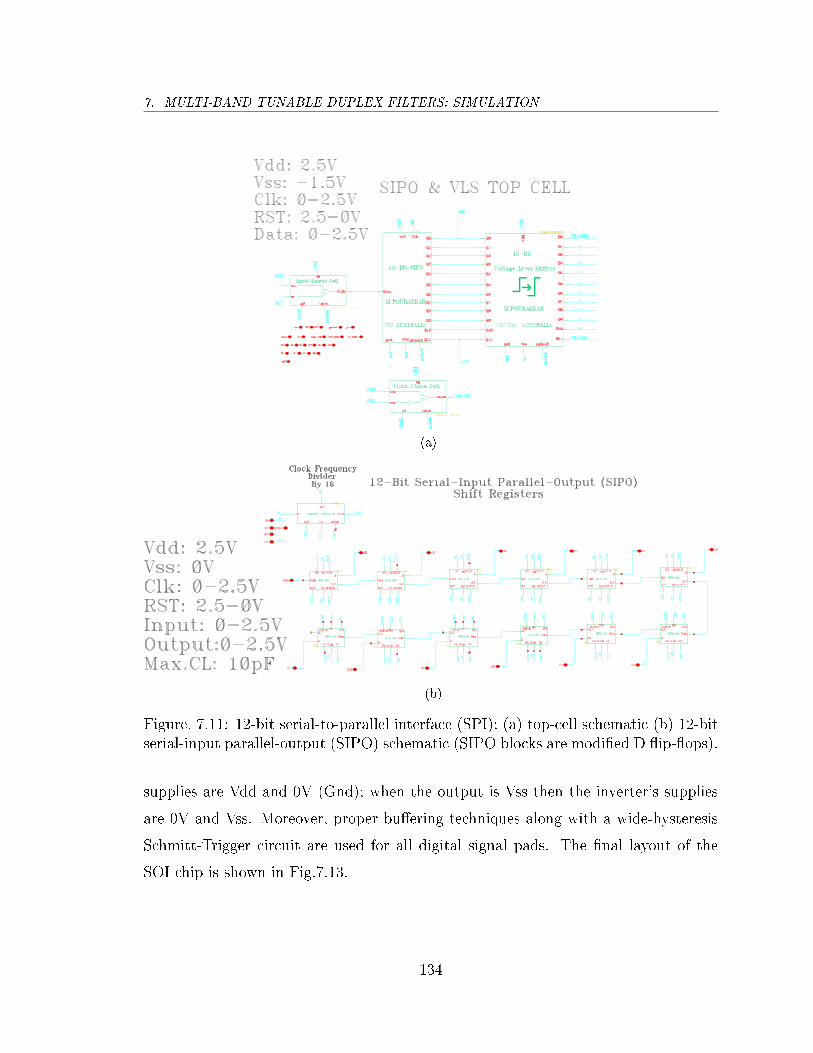
7. MULTI-BAND TUNABLE DUPLEX FILTERS: SIMULATION
(a)
(b)
Figure. 7.11: 12-bit serial-to-parallel interface (SPI): (a) top-cell schematic (b) 12-bitserial-input parallel-output (SIPO) schematic (SIPO blocks are modied D ip-ops).
supplies are Vdd and 0V (Gnd); when the output is Vss then the inverter's supplies
are 0V and Vss. Moreover, proper buering techniques along with a wide-hysteresis
Schmitt-Trigger circuit are used for all digital signal pads. The nal layout of the
SOI chip is shown in Fig.7.13.
134
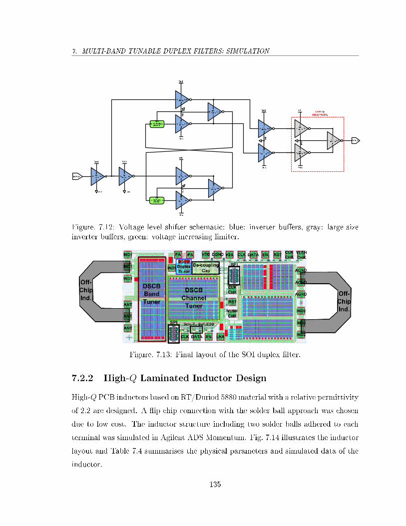
7. MULTI-BAND TUNABLE DUPLEX FILTERS: SIMULATION
1
Figure. 7.12: Voltage level shifter schematic: blue: inverter buers, gray: large sizeinverter buers, green: voltage increasing limiter.
Figure. 7.13: Final layout of the SOI duplex lter.
7.2.2 High-Q Laminated Inductor Design
High-Q PCB inductors based on RT/Duriod 5880 material with a relative permittivity
of 2.2 are designed. A ip chip connection with the solder ball approach was chosen
due to low cost. The inductor structure including two solder balls adhered to each
terminal was simulated in Agilent ADS Momentum. Fig. 7.14 illustrates the inductor
layout and Table 7.4 summarises the physical parameters and simulated data of the
inductor.
135
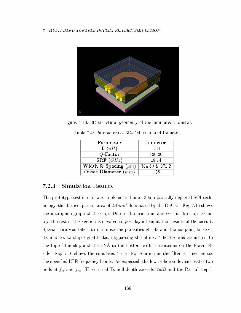
7. MULTI-BAND TUNABLE DUPLEX FILTERS: SIMULATION
Figure. 7.14: 3D structural geometry of the laminated inductor.
Table 7.4: Parameters of 3D-EM simulated Inductor.
Parameter InductorL (nH) 1.34Q-Factor 120.20
SRF (GHz) 18.74Width & Spacing (µm) 354.30 & 371.2Outer Diameter (mm) 1.58
7.2.3 Simulation Results
The prototype test circuit was implemented in a 130nm partially-depleted SOI tech-
nology, the die occupies an area of 2.4mm2 dominated by the DSCBs. Fig. 7.15 shows
the microphotograph of the chip. Due to the lead time and cost in ip-chip assem-
bly, the rest of this section is devoted to post-layout simulation results of the circuit.
Special care was taken to minimise the parasitics eects and the coupling between
Tx and Rx to stop signal leakage bypassing the lters. The PA was connected to
the top of the chip and the LNA to the bottom with the antenna on the lower left
side. Fig. 7.16 shows the simulated Tx to Rx isolation as the lter is tuned across
the specied LTE frequency bands. As expected, the low-isolation device creates two
nulls at ftx and frx. The critical Tx null depth exceeds 35dB and the Rx null depth
136
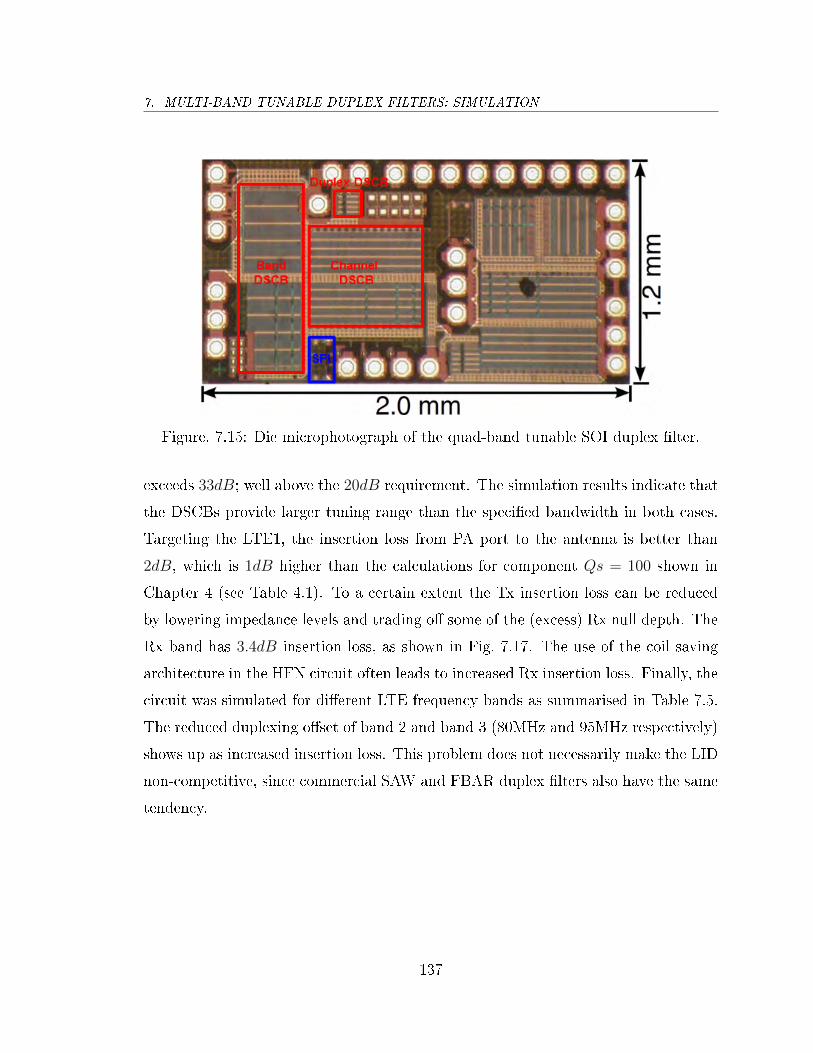
7. MULTI-BAND TUNABLE DUPLEX FILTERS: SIMULATION
Figure. 7.15: Die microphotograph of the quad-band tunable SOI duplex lter.
exceeds 33dB; well above the 20dB requirement. The simulation results indicate that
the DSCBs provide larger tuning range than the specied bandwidth in both cases.
Targeting the LTE1, the insertion loss from PA port to the antenna is better than
2dB, which is 1dB higher than the calculations for component Qs = 100 shown in
Chapter 4 (see Table 4.1). To a certain extent the Tx insertion loss can be reduced
by lowering impedance levels and trading o some of the (excess) Rx null depth. The
Rx band has 3.4dB insertion loss, as shown in Fig. 7.17. The use of the coil saving
architecture in the HFN circuit often leads to increased Rx insertion loss. Finally, the
circuit was simulated for dierent LTE frequency bands as summarised in Table 7.5.
The reduced duplexing oset of band 2 and band 3 (80MHz and 95MHz respectively)
shows up as increased insertion loss. This problem does not necessarily make the LID
non-competitive, since commercial SAW and FBAR duplex lters also have the same
tendency.
137
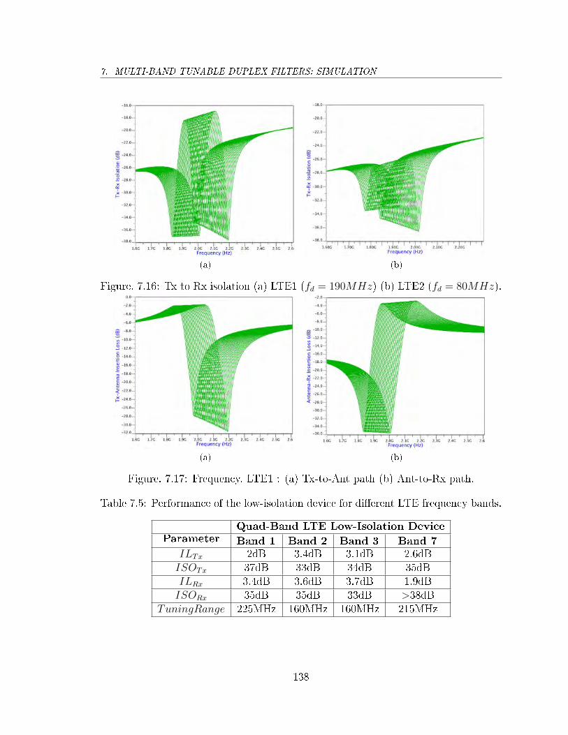
7. MULTI-BAND TUNABLE DUPLEX FILTERS: SIMULATION
(a) (b)
Figure. 7.16: Tx to Rx isolation (a) LTE1 (fd = 190MHz) (b) LTE2 (fd = 80MHz).
(a) (b)
Figure. 7.17: Frequency, LTE1 : (a) Tx-to-Ant path (b) Ant-to-Rx path.
Table 7.5: Performance of the low-isolation device for dierent LTE frequency bands.
ParameterQuad-Band LTE Low-Isolation Device
Band 1 Band 2 Band 3 Band 7ILTx 2dB 3.4dB 3.1dB 2.6dBISOTx 37dB 33dB 34dB 35dBILRx 3.4dB 3.6dB 3.7dB 1.9dBISORx 35dB 35dB 33dB >38dB
TuningRange 225MHz 160MHz 160MHz 215MHz
138

7. MULTI-BAND TUNABLE DUPLEX FILTERS: SIMULATION
7.3 Triple-band SOS Duplex Filter
A triple-band low-isolation device to cover LTE band 1,2, and 3 was designed. Fig.7.18
illustrates the building blocks of the chip. A 250nm Silicon-on-Sapphire (SOS) process
L1
Figure. 7.18: Multi-band tunable SOS duplex lter.
was chosen due to a generously free access by Peregrine Semiconductor. The FOM is
480fs for this process, almost two times higher than the SOI process of the previous
139
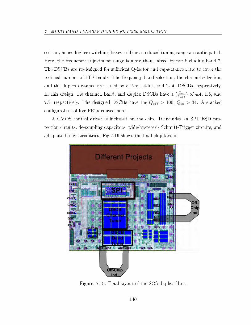
7. MULTI-BAND TUNABLE DUPLEX FILTERS: SIMULATION
section, hence higher switching losses and/or a reduced tuning range are anticipated.
Here, the frequency adjustment range is more than halved by not including band 7.
The DSCBs are re-designed for sucient Q-factor and capacitance ratio to cover the
reduced number of LTE bands. The frequency band selection, the channel selection,
and the duplex distance are tuned by a 2-bit, 4-bit, and 2-bit DSCBs, respectively.
In this design, the channel, band, and duplex DSCBs have a ( Con
Coff) of 4.4, 1.8, and
2.7, respectively. The designed DSCBs have the Qoff > 100, Qon > 34. A stacked
conguration of ve FETs is used here.
A CMOS control driver is included on the chip. It includes an SPI, ESD pro-
tection circuits, de-coupling capacitors, wide-hysteresis Schmitt-Trigger circuits, and
adequate buer circuitries. Fig.7.19 shows the nal chip layout.
Figure. 7.19: Final layout of the SOS duplex lter.
140

7. MULTI-BAND TUNABLE DUPLEX FILTERS: SIMULATION
7.3.1 Simulation Results
The triple-band duplex lter was fabricated in SOS 250nm Peregrine process, the
die occupies an area of 6mm2 dominated by the DSCBs and wide track routings
to accommodate more bond pads. Fig.7.20 displays the die photograph. The chip
was dened for ip-chip mounting, however, the multi-project silicon wafer (MPW)
was not post-processed for solder bumping. This was found to be too costly at the
University since the die needs to be singulated rst then gold stud bumps are manually
placed by a third-party company. No experimental work could therefore be done for
the chip. An attempt at wire bonding was unsuccessful due to the small area of the
pads. Only post-layout simulation results are given.
Figure. 7.20: Die microphotograph of the triple-band tunable SOS duplex lter.
Fig.7.21 shows the simulated frequency response of the lters tuned for the LTE1.
Two null-depths of 29dB and 32dB were achieved. These are well above the target
141
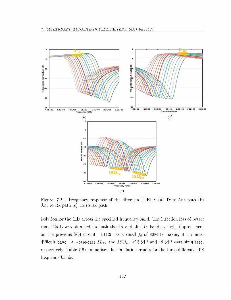
7. MULTI-BAND TUNABLE DUPLEX FILTERS: SIMULATION
(a) (b)
(c)
Figure. 7.21: Frequency response of the lters in LTE1 : (a) Tx-to-Ant path (b)Ant-to-Rx path (c) Tx-to-Rx path.
isolation for the LID across the specied frequency band. The insertion loss of better
than 2.5dB was obtained for both the Tx and the Rx band, a slight improvement
on the previous SOI circuit. LTE2 has a small fd of 80MHz making it the most
dicult band. A worse-case ILTx and ISORx of 3.8dB and 19.3dB were simulated,
respectively. Table 7.6 summarises the simulation results for the three dierent LTE
frequency bands.
142

7. MULTI-BAND TUNABLE DUPLEX FILTERS: SIMULATION
Table 7.6: Performance of the LID for dierent LTE frequency bands.
ParameterTriple-Band LTE LID
Band 1 Band 2 Band 3ILTx 2.1dB 3.8dB 3.2dBISOTx 29dB 19.3dB 20dBILRx 2.4dB 2.8dB 2.6dBISORx 32dB 25.5dB 27.7dB
TuningRange 320MHz 250MHz 250MHz
7.4 Summary
In this chapter, the impacts of die-to-substrate interconnections on a laminated
inductor are investigated. Solder ball and copper pillar signicantly reduce the con-
tact resistance between the silicon die and the PCB substrate. The simulation results
show that an inductor of 1.06nH designed on a thermoset substrate material and
adhered to a silicon chip via a couple of solder bumps, can achieve the quality factor
of 100. This inductor might be directly used inside a package for the tunable LIDs.
Two LC-based multi-band tunable low-isolation devices were presented. The rst
prototype was implemented in a 130nm SOI process and provides an isolation exceed-
ing 30dB at both Tx and Rx frequencies for each of four specied LTE bands (1, 2,
3, and 7). The fabricated circuit occupies an area of 2.0mm×1.2mm.The second prototype was demonstrated in an older technology, 250nm SOS. The
FET switch FOM eectively reduces the tuning range by one band. Simulations
show that the circuit can meet the isolation requirement of an LID covering three
LTE bands (1, 2, and 3). The insertion loss was better than 2.5dB across LTE1. The
size of the fabricated circuit is 3.0mm×2.0mm.The reported isolations can be further improved by applying an additional can-
cellation technique in an adaptive duplex solution. A summary of the measurement
and simulation results for the described LIDs are compared with some alternative
duplexer technologies in the next chapter.
143
Chapter 8
Conclusion
Nowadays, the LTE mobile communication standard is widely adopted throughout
the world. This new standard creates more design challenges for handset manufac-
turers in order to oer compatible mobile phones while maintaining low build cost.
Currently, the handset industry uses xed frequency bandwidth components for each
of the supported bands. In frequency division duplexing (FDD) systems, one such
component is the duplexer. This is a series of highly frequency selective SAW/FBAR
band-pass lters that are designed to isolate the sensitive receiver circuits from the
high-power transmitter output. These not only demonstrate low-noise, high-linearity
features but also have bulky size and require an additional o-chip inductor at their
balanced port. As indicated in Chapter 2 there are now 32 FDD bands in operation
somewhere in the world. To provide support for the many operating bands in the LTE
system, a set of duplexing lters and an RF switch are required for each frequency
band. In addition, a duplexer is required for each antenna in a MIMO system. These
drawbacks in traditional handset design provide the motivation to develop alternate
wideband tunable adaptive duplexer solutions for LTE handsets.
Chapter 3 reviewed current and proposed duplexer structures concluding with
the the wideband adaptive architecture of [53]. The need for multiple switched
duplexers is eliminated by using a low isolation device (LID) combined with a double
144

8. CONCLUSION
loop cancellation process. The goal of this Thesis was to develop a suitable LID. In
operation, the LID needs to create an initial isolation of about 15∼20dB and then an
active double-loop cancelling technique is used to further increase transmit-to-receive
isolation. The cancelling circuit can form up to two nulls at separate frequencies by
controlling the gain and phase settings of the loop coecients. The transmit data
and a pilot signal are used to control the cancelling loops. The original work used
a wideband circulator to create the initial isolation. Such a device is suitable for a
base station when the antenna system is always matched. However, this would not be
suitable for hand-held devices due to the undetermined impedance of the antenna. In
this work, the circulator is replaced by a tunable set of duplexing lters which enable
the scheme to cover multiple channels and frequency bands.
This thesis investigated two possible bandpass-bandstop networks, a low frequency
(passband) network (LFN) and a high frequency network (HFN). The theory devel-
oped in Chapter 4 showed the performance of the two networks is dominated by the
impedance level of the network elements and the Q of the primary resonant circuit
which must be high particularly when the duplexing oset is small. The impedance
level of the components determines the trade o between stop-band isolation and pass-
band insertion loss. It also determines the voltage enhancement, caused by network
resonances, which has a major impact on the switch design for the fabricated so-
lutions. High voltages in the OFF state require a large number of stacked devices
to share the voltage, which is signicantly easier when the devices are implemented
on an insulating substrate, such as Silicon-on-Sapphire (SOS) or Silicon-on-Insulator
(SOI). The use of dual circuits provides more impedance level choices and therefore
trade-os between voltage and current levels within the components.
Chapter 5 briey described the SOI and SOS processes and compared them to
normal bulk CMOS. The Ron × Coff gure of merit (FOM) for a FET switch was
introduced as was the biasing and stacking operation required for high voltage op-
eration. Low FOM's are preferable and the SOI process had the best performance.
Simulations of an eight transistor stack illustrated voltage sharing in the OFF state
145
8. CONCLUSION
and distortion generation in the ON state.
In Chapter 6, both a fully-integrated LID and a discrete LID were designed and
tested, targeting LTE band 1. The former is a digitally tunable LC-based duplex
lter fabricated in 250-nm SOS process; it measured 19dB of isolation at the transmit
frequency and 14dB of isolation at the receive frequency while achieving the required
tuning range of 60MHz for LTE1. However the insertion loss was poor particularly
on the receiver side (≈ 5dB). SOI/SOS inductors have higher Q than their CMOS
counterparts, but in this application the Q's are far short of what is needed. O-chip
inductors are thus necessary to reach targeted performance. The discrete solution
used o-chip passives and commercial o-the-shelf digitally tuned capacitors (DTC)
mounted on a PCB. The null-depths were improved to below −25dB and the insertion
loss reduced to 3.6dB. The commercial DTCs were not optimised for this application
and further improvements can be expected by custom designing the switches and
using good Figure of Merit Transistors.
Today's smart phones need to operate in dierent operating bands and standards
due to roaming purpose. Therefore, multi-band duplexers are fruitful. In Chapter 7,
two partially-integrated solutions for multi-band tunable LIDs were proposed. The
rst prototype is a quad-band tunable LID which supports four common LTE bands
(1,2,3, and 7). It was implemented using a 130-nm partially-depleted SOI process.
The simulation results showed that the isolation exceeded 30dB at both Tx and Rx
frequencies for each intended LTE band. The circuit was fabricated and occupies
an area of 2.4mm2. The second prototype was a cut-down version of the previous
chip (only triple-band) which covered LTE 1,2,3. The 250-nm SOS process used for
implementation had a poorer FOM which restricted the tuning range. The simulated
isolation was almost 30dB for LTE1. However, it was degraded to about 19dB for
LTE2 with the smaller duplex oset of 85MHz.
Table 8.1 compares some alternative duplexer technologies. The circulator used
in [53] is wideband (1 octave) but is very bulky. Small circulators such as in [88]
have a narrow bandwidths (7%) making them unsuitable for the larger duplex osets
146
8. CONCLUSION
(10%). Couplers have a wide bandwidth but suer from a high insertion loss on
the coupled port [89], reducing this is at the expense of increasing the loss on the
direct port. A 3dB coupler has a minimum of 3dB loss on both ports. Hybrid
balancing networks have a wide bandwidth [40]. However, like couplers, there is a
3dB loss in the balancing network. There is also the problem of maintaining balance at
both Tx and Rx frequencies concurrently. Dual antennas, if they are closely spaced,
have narrow bandwidths [20]. Larger spacing increases bandwidth and real-estate.
Filtering techniques are less aected by antenna mismatch compared to couplers
and circulators. SAW devices have good isolation and insertion loss but are not
tunable [90]. The solutions proposed here are tunable, but have higher insertion loss
than the SAW devices they are meant to replace. The PCB solution is competitive
in terms of IL as predicted by EM-simulations, but the measured results missed the
target by 1dB on the Tx side.
147

8. CONCLUSION
Table8.1:
Perform
ance
summaryandcomparison.
Ref.
Circulator
[88]
Coupler
[89]
EBD
[40]
Dual
Ant.[20]
SAW
Dup.[90]
Thiswork
Tec h.
Ferrite
0.18-um
CMOS
90-nm
CMOS
LC
Matching
FR4PCB
Surface
Acoustic
Wave
Lumped
LC250-nm
SOS
Lumped
LCFR4
PCB
Quad-
band
SOI
Triple-
band
SOS
Freq.
Range
(MHz)
1880-2025
600-1300
1700-2200
2420-2500
1950-2140
1920-
2170
1830-2220
1710-2170
1710-2690
ILTx
0.25dB
0.8dB
4.7dB†
0dB
1.8+0.9*=
2.7dB
Sim
.Meas.
Sim
.Meas.
Sim
.‡Sim
.‡
3.8dB
3.8dB
2.6dB
3.7dB
2.0dB
2.1dB
Rx
16dB
>3.8dB†
2.4+0.9*=
3.3dB
4.8dB
5.8dB
3.5dB
3.8dB
3.4dB
2.4dB
ISO
Tx
23dB
>20dB
70dB
>15dB
50dB
17.5dB
19dB
28dB
25dB
35dB
29dB
Rx
40dB
42dB
13.5dB
14dB
28dB
31dB
37dB
32dB
Tuning
Range(%
)NO
NO
29.4
NO
NO
3.0
4.8
8.2-11
12
11.5
16.4
Size
(mm
2)
412
0.09§
2.52
1155
3.2
2.42
121¶
2.4
6
∗ Assumes
PeregrinePE42694SP9Tswitch
and0.3dBPCBloss.
† Assumes
antennabalunwith0.8dBloss.
§ Core
size
withoutthecapacitorsin
PCB.
¶Core
size
withde-em
bedded
SMAlaunches
andtraces.
‡ SimulationresultsforLTEband1.
148
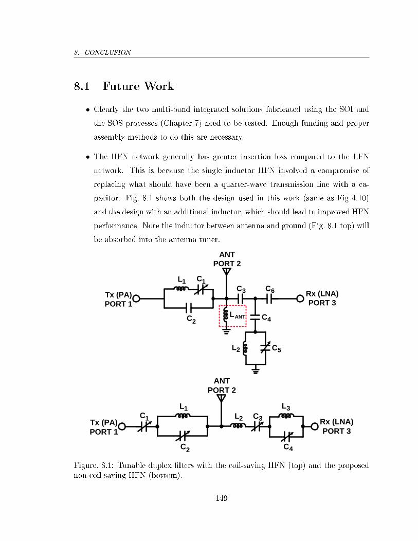
8. CONCLUSION
8.1 Future Work
• Clearly the two multi-band integrated solutions fabricated using the SOI and
the SOS processes (Chapter 7) need to be tested. Enough funding and proper
assembly methods to do this are necessary.
• The HFN network generally has greater insertion loss compared to the LFN
network. This is because the single inductor HFN involved a compromise of
replacing what should have been a quarter-wave transmission line with a ca-
pacitor. Fig. 8.1 shows both the design used in this work (same as Fig 4.10)
and the design with an additional inductor, which should lead to improved HFN
performance. Note the inductor between antenna and ground (Fig. 8.1 top) will
be absorbed into the antenna tuner.
C
L
CL
C
Tx (PA)
PORT 1
ANT
PORT 2
Rx (LNA)
PORT 3
1 1
2
3
2
C6
C4
C5
LANT
L
C
L
Tx (PA)
PORT 1
ANT
PORT 2
Rx (LNA)
PORT 3
1
1
3
L2 C3
C2 C4
Figure. 8.1: Tunable duplex lters with the coil-saving HFN (top) and the proposednon-coil saving HFN (bottom).
149

8. CONCLUSION
• More isolation nulls are needed to accommodate dierent carrier-aggregation
(CA) scenarios. A possible solution is to cascade more LFN/HFN networks in
each transmission path. For instance, a tunable duplex lter topology for a CA
scenario with two transmit and two receive frequencies is shown in Fig. 8.2. The
structure creates two isolation nulls in both the Tx and the Rx bands.
C
L
CL
C
Tx (PA)
PORT 1
ANT
PORT 2
Rx (LNA)
PORT 3
2
1
3
4
3
C9
C5
C6
LANT
L4
C7
C
L
C
1
2
8
Figure. 8.2: Proposed tunable duplex lters structure to support a carrier-aggregationscenarios ((fTx1, fTx2) and (fRx1, fRx2)).
• Other Ph.D. students have designed the gain-phaser adjusters for the cancelling
loops and the pilot sub-system for the adaptive duplexer. Integration of these
with the LID in a single silicon chip is the ultimate aim.
150
References
[1] Ericsson, Ericsson Mobility Report, Ericsson, Tech. Rep., June 2014.
[2] N. Netwroks, LTE-Advanced Carrier Aggregation Optimization, Nokia
Netwroks, Tech. Rep., 2015.
[3] J. Mitola, The software radio architecture, IEEE Communication Magazine,
vol. 33, no. 5, pp. 2638, May 1995.
[4] S. Kannangara and M. Faulkner, Adaptive duplexer for multiband transre-
ceiver, Proceedings of IEEE Radio and Wireless Conference (RAWCON), pp.
381384, August 2003.
[5] A. Rao and G. Crupi, Microwave Wireless Communications: From
Transistor to System Level. Elsevier Science, 2016. [Online]. Available:
https://books.google.com.au/books?id=J\_IQCgAAQBAJ
[6] Third-Generation Partnership Project (3GPP), Online, 2015. [Online].
Available: http://www.3gpp.org/about-3gpp
[7] E. Commission, Mobile communications: Fresh 50 million EU research grants
in 2013 to develop '5G' technology, Europa.eu, Tech. Rep., February 2013.
[8] S. Sesia, I.Touk, and M. Baker, LTE - The UMTS Long Term Evolution: From
Theory to Practice, 2nd ed. John Wiley, 2011, vol. 6.
151
REFERENCES
[9] 3GPP, LTE; Evolved Universal Terrestrial Radio Access (E-EUTRA); User
Equipment (UE) Radio Transmission and Reception, 3GPP, 2015.
[10] H. J. Carlin and A. B. Giordano, Network theory: an introduction to reciprocal
and non-reciprocal circuits. Prentice-Hall, 1964.
[11] R. E. Jones, C. Ramiah, T. Kamgaing, S. K. Banerjee, C.-T. Tsai, H. G. Hughes,
A. P. D. Silva, J. Drye, L. Li, W. Blood, Q. Li, C. R. Vaughan, R. Miglore, D. Pe-
nunuri, R. Lucero, D. R. Frear, and M. F. Miller, System-in-a-package Integra-
tion of SAW RF RX Filter stacked on a Transceiver Chip, IEEE Transactions
on Advanced Packaging, vol. 28, no. 2, pp. 310319, February 2005.
[12] M.Dubois, C.Billard, C.Muller, G.Parat, and P.Vincent, Integration of High-
Q BAW Resonators and Filters above IC, IEEE ISSCC Techical Digest, pp.
392394, February 2005.
[13] J.-W. Lobeek and A. Smolders, Design and Industrialisation of Solidly-Mounted
BAW lters, IEEE MTT-S International Microwave Symposium Digest, pp.
386389, June 2006.
[14] D.Feld, T.Jamneala, C.Wade, S.Fazzio, D.Hula, and A.Chien, Low Insertion
Loss, High Rejection Handsets Duplexer for UMTS-1 (WCDMA) Band, IEEE
International Ultrasonics Symposium Proceedings, vol. 1, pp. 101104, September
2005.
[15] K.Nam, Y.Park, B.Ha, C.Kim, J.Shin, S.Yun, J.Pak, G.Park, and I.Song, Mono-
lithic 1-Chip FBAR Duplexer for WCDMA Handsets, Journal of Sensors and
Actuators A: Physical, vol. 143, no. 1, pp. 162168, May 2008.
[16] K.Kawai, H.Okazaki, and S.Narahashi, Tunable Ring Resonator Filter for Du-
plexer, Proceedings of the 38th European Microwave Conference (EuMC), pp.
603606, October 2008.
152

REFERENCES
[17] K.Wang, D.Clark, L.H.Camnitz, and P.Bradley, A UMTS-900 Duplexer, IEEE
International Ultrasonics Symposium Proceedings, vol. 1, pp. 899902, November
2008.
[18] Murata. (2015) SAW Duplexer. [Online]. Available: http://www.Murata.co.jp
[19] A. Technologies. (2015) FBAR Duplexer. [Online]. Available: http://www.
avagotech.com/products/wireless/fbar/duplexers
[20] S. Chen, Y. Wang, and S. Chung, A Decoupling Technique for Increasing the
Port Isolation Between Two Strongly Coupled Antennas, IEEE Transaction
Antennas Propagation, vol. 56, no. 2, pp. 36503658, December 2008.
[21] G. R. Kenworthy, Self-cancelling full-duplex RF communication system, Patent
5,691,978, November, 1997.
[22] M. Duarte, Full-duplex wireless: design, implementation and characterization,
Ph.D. dissertation, Rice University, 2010.
[23] A. K. Khandani, Methods for spatial multiplexing of wireless two-way channels,
Patent 7,817,641, 2010.
[24] K. Haneda, E. Kahra, S. Wyne, C. Icheln, and P. Vainikainen, Measurement of
loop-back interference channels for outdoor-to-indoor full-duplex radio relays,
European Conference on Antennas and Propagation, pp. 15, April 2010.
[25] A. Chebihi, C. Luxey, A. Diallo, P. Thuc, and R. Staraj, A novel isolation
technique for closely spaced PIFAs for UMTS mobile phones, IEEE Antennas
and Wireless Propagation Letters, vol. 7, pp. 665668, November 2008.
[26] W. Kim, M. Lee, J. Kim, H. Lim, J. Yu, B. Jang, and J. Park, A passive
circulator for RFID application with high isolation using a directional coupler,
36th IEEE European Microwave Conference (EuMC), pp. 196199, September
2006.
153
REFERENCES
[27] M. Koller and R. Kung, Adaptive carrier supression for UHF RFID using dig-
itally tunable capacitors, IEEE European Microwave Conference (EuMC), pp.
943946, October 2013.
[28] O. Alrabadi, A. Tatomirescu, M. Knudsen, M. Pelosi, and G. Pedersen, Break-
ing the Transmitter-Receiver Isolation Barrier in Mobile Handsets With Spatial
Duplexing, IEEE Transactions on Antennas and Propagation, vol. 61, no. 4, pp.
22412251, April 2013.
[29] E. Tsakalaki, O. Alrabadi, A. Tatomirescu, E. d. Carvalho, and G. Pedersen,
Concurrent Communication and Sensing in Cognitive Radio Devices: Chal-
lenges and an Enabling Solution, IEEE Transactions on Antennas and Propa-
gation, vol. 62, no. 3, pp. 11251137, March 2014.
[30] M. Pelosi, O. Alrabadi, A. Tatomirescu, and G. Pedersen, Isolation potential
of Capacitive Coupling Elements for smartphones using spatial duplexing, 7th
European Conference on Antennas and Propagation (EuCAP), pp. 20612062,
April 2013.
[31] O. Leisten, R. Collier, and R. Bates, Distributed ampliers as duplexer/low
crosstalk bidirectional elements in S-band, Electronics Letters, vol. 24, no. 5,
pp. 264265, March 1988.
[32] S. Balamurugan and P. N. Shastry, A Novel Electronically Tunable Active Du-
plexer for Wireless Transceiver Applications, IEEE Transactions on Microwave
Theory and Techniques, vol. 54, no. 6, pp. 25842592, June 2006.
[33] J. B. Beyer, S. N. Prasad, J. E. Nordman, R. C. Becker, and G. Hohenwarter,
MESFET Distributed Amplier Design guidelines, IEEE Transactions on Mi-
crowave Theory and Techniques, vol. 32, no. 3, pp. 268275, March 1984.
[34] Z.El.Khatib, L.MacEachern, and S.A.Mahmoud, Fully-Integrated CMOS Bidi-
rectional Distributed Amplier as Tunable Active Duplexer For Wireless
154
REFERENCES
Transceiver Applications, Proceedings of the 1st Microsystems and Nanoelec-
tronics Research Conference (MNRC), pp. 58, October 2008.
[35] H.Khatri, P.S.Gudem, and L.E.Larson, Integrated RF Interference Suppression
Filter Design Using Bond-Wire Inductors, IEEE Transactions on Microwave
Theory and Techniques, vol. 56, no. 5, pp. 10241034, May 2008.
[36] T.H.Lee, Planar Microwave Engineering. Cambridge, U.K.: Cambridge Uni-
versity Press, 2004.
[37] E. Sartori, Hybrid Transformers, IEEE Transactions on Parts, Materials and
Packaging, vol. 4, no. 3, September 1968.
[38] M.Mikhemar, H.Darabi, and A.Abidi, A Tunable Integrated Duplexer with
50dB Isolation in 40nm CMOS, IEEE International Solid-State Circuits Con-
ference Digest, pp. 386388, February 2009.
[39] M. Mikhemar, H. Darabi, and A. Abidi, A Multiband RF Antenna Duplexer on
CMOS: Design and Performance, IEEE Journal of Solid-State Circuits, vol. 48,
no. 9, pp. 20672077, September 2013.
[40] S. H. Abdelhalem, P. S. Gudem, and L. E. Larson, Hybrid Transformer-Based
Tunable Dierential Duplexer in a 90-nm CMOS Process, IEEE Transactions
on Microwave Theory and Techniques, vol. 61, no. 3, pp. 13161326, 2013.
[41] I. Lu, Y. Chi-Yao, C. Yen-Horng, C. Lan-Chou, C. Sun, T. Chih-Chun, and
G. Chien, A SAW-less GSM/GPRS/EDGE receiver embedded in a 65nm CMOS
SoC, IEEE Solid-State Circuits Conference Digest of Technical Papers (ISSCC),
pp. 364366, February 2011.
[42] A. Roussel, C. Nicholls, and J. Wight, Frequency agile RF feedforward noise
cancellation system, IEEE Radio and Wireless Symposium, pp. 109112, Jan-
uary 2008.
155

REFERENCES
[43] , Frequency agile bandstop lter (FABSF), IEEE MTT-S International
Microwave Symposium Digest, pp. 10991102, June 2008.
[44] H. Darabi, A. Mirzaei, and M. Mikhemar, Highly Integrated and Tunable
RF Front Ends for Recongurable Multiband Transceivers: A Tutorial, IEEE
Transactions on Circuits and Systems I: Regular Papers, vol. 58, no. 9, pp. 2038
2050, September 2011.
[45] S. Heinen and R. Wunderlich, High dynamic range RF frontends from multiband
multistandard to Cognitive Radio, Semiconductor Conference Dresden (SCD),
pp. 18, September 2011.
[46] V. Aparin, G. Ballantyne, and C. J. Persico, An Integrated LMS Adaptive Filter
of TX Leakage for CDMA Receiver Front Ends, IEEE Journal of Solid State
Circuits, vol. 41, no. 5, pp. 117182, May 2006.
[47] T. Harald, K. Walter, D. Herbart, and G. Roman, Transmitter leakage cancel-
lation circuit for co-located GPS receiver, Patent 1 091 497, April, 2001.
[48] E. M. S. K. D.Bharadia, Full-duplex radios, ACM Special Interest Group on
Data Communication (SIGCOMM), pp. 375386, August 2013.
[49] W. Schacherbauer, A. Springer, T. Ostertag, C. C. W. Ruppel, and R. A. Weigel,
A exible multi band front end for software radios using high IF and active
interference cancellation, IEEE MTT-S International Microwave Symposium
Digest, vol. 2, pp. 10851088, 2001.
[50] A. Masmoudi and T. Le-Ngoc, Residual Self-Interference after Cancellation in
Full-Duplex Systems, IEEE International Conference on Communications, pp.
375386, June 2014.
[51] T. O'Sullivan, R. York, B. Noren, and P. Asbeck, Adaptive duplexer imple-
mented using single-path and multipath feedforward techniques with BST phase
156

REFERENCES
shifters, IEEE Transactions on Microwave Theory and Techniques, vol. 53,
no. 1, pp. 106114, January 2005.
[52] S. Kannanagara, Adaptive Duplexer for Software Radio, Ph.D. dissertation,
Victoria University, Melbourne, Australia, 2006.
[53] S.Kannangara and M.Faulkner, Analysis of an Adaptive Wideband Duplexer
With Double-Loop Cancellation, IEEE Transactions on Vehicular Technology,
vol. 56, no. 4, pp. 19711982, July 2007.
[54] P. Vizmuller, RF Design Guide systems, circuits, and equations. Boston: Artech
House, 1954, pp. 233-237.
[55] M. Pourakbar, L. Linton, M. Tormanen, and M. Faulkner, Tunable duplex lter
for adaptive duplexers of advanced LTE handsets, IEEE MTT-S International
Microwave Symposium Digest, pp. 14, June 2013.
[56] T. Onzuka, K. Noguchi, S. Yoshimoto, and Y. Yamamoto, SAW duplexers with-
out lambda/4 phase shifter for CDMA cellular phone systems, Proceedings of
IEEE Ultrasonics Symposium, vol. 2, pp. 966969, August 2004.
[57] H. K. Yang, H.-M. Cho, and J.-C. Park, The eects of stripline geometries
for phase shifting on SAW antenna duplexer, Proceedings of IEEE Ultrasonics
Symposium, vol. 1, pp. 115118, October 1998.
[58] J.-P. Colinge and R. W. Bower, Silicon-on-lnsulator Technology, Bulletin of
the Material Research Society (MRS), vol. 23, no. 12, pp. 1315, December 1998.
[59] J.-P. Colinge, Silicon-on-lnsulator Technology: Past Achievements and Future
Prospects, Bulletin of the Material Research Society (MRS), vol. 23, no. 12, pp.
1619, December 1998.
[60] , Silicon-on-Insulator Technology: Materials to VLSI, 2nd ed. Springer
Science and Business Media, 2013.
157

REFERENCES
[61] J. L. Leray, E. Dupont-Nivet, J. F. Pere, Y. M. Coic, M. Raaelli, A. J. Auberton-
Herve, M. Bruel, B. Giard, and J. Margail, CMOS/SOI hardening at 100 Mrad
(SiO2), IEEE Transactions on Nuclear Science, vol. 37, no. 6, pp. 20132019,
December 1990.
[62] L. Hite, H. Lu, T. Houston, D. Hurta, and W. Bailey, An seu resistant 256k soi
sram, IEEE Transaction on Nuclear Science, vol. 39, p. 2121, 1992.
[63] K. Izumi, SIMOX (Separation by Implantation of Oxygen), Bulletin of the
Material Research Society, vol. 23, no. 12, pp. 2024, 1998.
[64] D. J. Godbey, H. L. Hughes, and F. J. Kub, Method of producing a thin silicon-
on-insulator layer, Patent US5 013 681 A, May, 1991.
[65] M. Bruel, Silicon on insulator material technology, IEEE Electronics Letters,
vol. 31, no. 14, pp. 12011202, 1995.
[66] E. Culurciello, Silicon-on-Sapphire Circuits and Systems. McGraw Hill, 2010.
[67] G. Imthurn, The History of Silicon-on-Sapphire, Peregrine Semiconductor Cor-
poration, Tech. Rep., 2007.
[68] Peregrine, Ultra CMOS 0.5um design manual, Peregrine Semiconductor
Corporation, 2010. [Online]. Available: htpp://www.psemi.com
[69] , UGX rev. 1.9 UltraCMOS 0.25um spice models, Peregrine Semiconductor
Corporation, 2010.
[70] R. Amirkhanzadeh, H.Sjoland, A. Tikka, and M. Faulkner, Comparative analy-
sis of switching performance of transistors in SOS process for RF applications,
IEEE Asia-Pacic Conference on Circuits and Systems, pp. 11111114, Decem-
ber 2010.
[71] STMicroelectronics, HCMOS9 SOI Design Rules Manual, STMicroelectronics,
2013.
158
REFERENCES
[72] M. Burgener, CMOS SOS Switches Oer Useful Features, High Integration,
Microwave and RF Magazine, pp. 107118, August 2001.
[73] D. Kelly, C. Brindle, C. Kemerling, and M. Stuber, The state-of-the-art of
silicon-on-sapphire CMOS RF switch, IEEE Compound Semiconductor Inte-
grated Circuit Symposium (CSIC), pp. 48, November 2005.
[74] B. Razavi, RF Microelectronics, 2nd ed. Prentice Hall, 2011.
[75] C. W. Liu and M. Damgaard, IP2 and IP3 nonlinearity specications for
3G/WCDMA receivers, High Frequency Electronics, pp. 110, June 2009.
[76] M. B. Shifrin, P. J. Katzin, and Y. Ayasli, Monolithic FET structures for high-
power control component applications, IEEE Transaction on Microwave Theory
and Technique, vol. 37, no. 12, pp. 21342141, December 1989.
[77] C. Tinella, F. Gianesello, D. Gloria, C. Raynaud, P. Delatte, A. Engelstein,
J. Fournier, P. Benech, and J. Jomaah, Partially depleted CMOS SOI tech-
nology for low power RF applications, European Gallium Arsenide and Other
Semiconductor Application Symposium (EGAAS), pp. 101104, November 2005.
[78] T. Ranta, Method and apparatus for use in digitally tuning a capacitor in
an integrated circuit device, Patent US 20 110 002 080A1, January 06, 2011.
[Online]. Available: https://www.google.com/patents/US20110002080
[79] E. A. Standard, ESD Sensitivity Testing: Human Body Model (HBM)-
Component Level, ESD Association Standard, Tech. Rep., 1993.
[80] , ESD Sensitivity Testing: Machine Model (MM)-Component Level, ESD
Association Standard, Tech. Rep., 1994.
[81] J. L. Hilbert, Tunable RF Components and Circuits: Applications in Mobile
Handsets. CRC Press, 2015.
159
REFERENCES
[82] J. Zeng, C. Wang, and A. Sangster, Theoretical and Experimental Studies of
Flip-Chip Assembled High- Q Suspended MEMS Inductors, IEEE Transactions
on Microwave Theory and Techniques, vol. 55, no. 6, pp. 11711181, June 2007.
[83] A. Nazarian, L. Tiemeijer, D. John, J. van Steenwijk, M. de Langen, and R. M. T.
Pijper, A Physics-Based Causal Bond-Wire Model for RF Applications, IEEE
Transactions on Microwave Theory and Techniques, vol. 60, no. 12, pp. 1171
1181, December 2012.
[84] J. H. Lau, Flip Chip Technologies, McGraw-Hill, p. 560, 1996.
[85] R. Pratap, D. Staiculescu, S. Pinel, J. Laskar, and G. May, Modeling and sen-
sitivity analysis of circuit parameters for ip-chip interconnects using neural
networks, IEEE Transactions on Advanced Packaging, vol. 28, no. 1, pp. 7178,
February 2005.
[86] S. S. Mohan, M. Hershenson, S. Boyd, and T. Lee, Simple Accurate Expressions
for Planar Spiral inductances, IEEE Journal of Solid-State Circuits, vol. 34,
no. 10, pp. 14191424, October 1999.
[87] J. Warner, C. Savalia, and M. Ingham, High Performance Multilayer PCBs
Design and Manufacturability, Electronics Manufacturing Technical Articles,
October 2013. [Online]. Available: http://www.smtnet.com/library/index.cfm?
fuseaction=view_article&article_id=1942
[88] Skyworks. (2011) Circulator MAFR-000618-000001 datasheet. Woburn,
USA. [Online]. Available: http://www.skyworksinc.com/uploads/documents/
201561A.pdf
[89] L. Ye, Y. Zheng, J. Wang, H. Liao, and R. Huang, Miniature CMOS Stacked
Spiral-Coupled Directional Coupler With -67-dB Isolation and -0.8-dB Insertion
Loss, IEEE Electron Device Letter, vol. 33, no. 7, pp. 919921, July 2012.
160
REFERENCES
[90] EPCOS. (2013) SAW Duplexer B8510 datasheet. Munich, Germany. [Online].
Available: http://en.tdk.eu/inf/40/ds/mc/B8510.pdf
161