
Copyright by Jacob S. Schneider 2005users.ece.utexas.edu/~adnan/comm/js_ms_05.pdf · 2006-04-20 ·...
83
Copyright by Jacob S. Schneider 2005
Transcript of Copyright by Jacob S. Schneider 2005users.ece.utexas.edu/~adnan/comm/js_ms_05.pdf · 2006-04-20 ·...

Copyright
by
Jacob S. Schneider
2005
Error Correction Logic for Wireless USB
by
Jacob S. Schneider, B.S.
Report
Presented to the Faculty of the Graduate School of
The University of Texas at Austin
in Partial Fulfillment
of the Requirements
for the Degree of
Masters of Science in Engineering
The University of Texas at Austin
December 2005

Error Correction Logic for Wireless USB
Approved by Supervising Committee:

Dedication
To my wife Anne, who moved to the great city of Austin and always supported me
through the trials and tribulations of juggling school and work.

v
Acknowledgements
The author would like to acknowledge the significant guidance received from
Adnan Aziz, Mark McDermott, and Saf Asghar, as well as the contributions of project
members Dan Dankert, Sanjeev Gokhale, and Dimitry Patent. Finally, he would like to
give special recognition to Intel Corporation for providing the opportunity to pursue this
degree.
December 2005
vi
Abstract
Error Correction Logic for Wireless USB
Jacob S. Schneider, M.S.E.
The University of Texas at Austin, 2005
Supervisor: Adnan Aziz
This paper will present the motivations behind and actions taken to create a
wireless device compatible with Universal Serial Bus 2.0 (USB). This device is intended
to be used in portable devices needing a USB link to a host controller, serving as a
replacement for the normal wired transceiver. Integrating a small wireless transceiver
with standard USB 2.0 host, hub, and function controllers in lieu of the standard wired
connection would help to eliminate nests of wires without compromising the usefulness
of the broad range of designs that already conform to the USB specifications. Wireless
mice and keyboards can already be purchased that can connect to USB, but these devices
are all low speed human interface devices. The proposed transceivers would extend this
wireless capability to full-speed and high-speed USB 2.0 protocols; allowing for devices
such as disk drives, digital cameras, and others to connect wirelessly to a PC while still
utilizing the robustness of the USB protocol.
vii
Area and power savings were the two main focal points in implementing this
transceiver. A unique protocol layer was developed for this application to aid the
transmission and reception of various analog USB states. Both digital and analog clock
recovery systems were employed as well as an error correction block to aid in bit error
rate minimization. A simple ROM based CORDIC sine wave generation scheme was
employed for the reference clocks in the local oscillators. Emphasis was placed in the RF
front end to limit the number of discrete components needed to transmit and receive.
Finally, a combination of MatLab, Hspice, and VCS simulations were used to determine
and fine tune operation of both the digital and analog components.
This specific report will focus on the top level architecture and error correction
that was employed in this design. The error correction helps reduce the bit error rate that
occurs due to the wireless channel and noise from the various system components. It
does require some additional circuitry to perform the encoding and decoding, as well as a
few other design features to enable the use of desirable clock frequencies. The encoding
scheme employed here is a 1/3 convolutional code with Viterbi decoding.

viii
Table of Contents
List of Tables ...................................................................................................... x
List of Figures .................................................................................................... xi
ERROR CORRECTION LOGIC FOR WIRELESS USB 1
Chapter 1: Introduction....................................................................................... 1
1.1 Design Space ..................................................................................... 1
1.2 Overall Design Problem..................................................................... 1
1.3 Specific Design Problem.................................................................... 3
Chapter 2: Top-Level Architecture ...................................................................... 5
2.1 Desired Characteristics and Features: ................................................. 5
2.2 USB 2.0 Requirements....................................................................... 6
2.3 Transceiver Requirements.................................................................. 7
2.4 Clocking and Wireless Requirements ................................................. 8
2.5 USB Interface .................................................................................... 8
2.6 Top Level Details............................................................................. 10
2.7 Transmit and Receive Details ........................................................... 14
2.8 Clocking Details .............................................................................. 17
Chapter 3: Error Correction .............................................................................. 19
3.1 Introduction ..................................................................................... 19
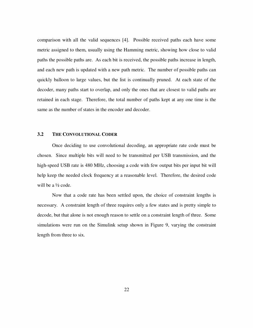
3.2 The Convolutional Coder ................................................................. 22
3.3 The Viterbi Decoder......................................................................... 29
Chapter 4: Error Correction Simulation Results ................................................ 31
4.1 Matlab Simulation Results ............................................................... 31
4.2 Verilog Simulation Results............................................................... 36
4.2.1 Encoder Testing ...................................................................... 37
4.2.2 Encoder/Decoder Pair Test Results.......................................... 38
4.2.3 Decoder Error Correction Test Results .................................... 40
4.2.4 Encoder/Decoder Summary..................................................... 44
ix
Chapter 5: Project Integration and Conclusion.................................................. 45
5.1 Digital USB Interface and Error Correction Circuitry....................... 46
5.2 Clock Recovery Mechanism............................................................. 47
5.3 Low-Noise Amplifier, Power Amplifier, and Antenna...................... 49
5.4 Frequency Synthesizer ..................................................................... 50
5.5 Summary ......................................................................................... 51
Appendices........................................................................................................... i
A1 Acronym Definitions........................................................................... i
A2 Matlab Convolutional Code and Viterbi Decoding Source Code ........ ii
A3 Verilog Code for the Convolutional Encoder...................................... v
A4 Verilog Code for the Viterbi Decoder............................................... xii
Works Cited ................................................................................................... xviii
Vita .................................................................................................................. xix
x
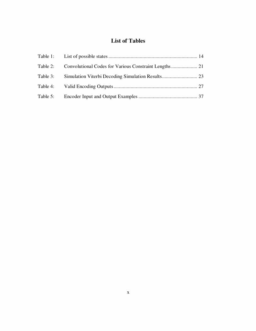
List of Tables
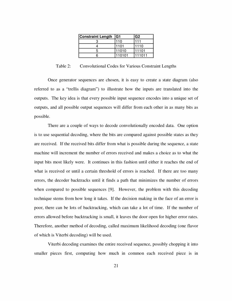
Table 1: List of possible states .................................................................... 14
Table 2: Convolutional Codes for Various Constraint Lengths .................... 21
Table 3: Simulation Viterbi Decoding Simulation Results........................... 23
Table 4: Valid Encoding Outputs ................................................................ 27
Table 5: Encoder Input and Output Examples ............................................. 37
xi
List of Figures
Figure 1: System-Level Block Diagram.......................................................... 6
Figure 2: USB Transceiver Details [5]............................................................ 9
Figure 3: Wireless USB Transceiver Top Level Diagram ............................. 11
Figure 4: Encoder Block Diagram ................................................................ 16
Figure 5: Decoder Block Diagram................................................................ 16
Figure 6: Clock Selection Circuitry .............................................................. 17
Figure 7: Reset Detection Circuitry .............................................................. 18
Figure 8: Sample Convolutional Coder......................................................... 20
Figure 9: Simulink Viterbi Decoding Simulation.......................................... 23
Figure 10: Wireless USB Convolutional Coder .............................................. 24
Figure 11: Convolutional Coder State Machine .............................................. 25
Figure 12: Convolutional Coder Trellis Diagram............................................ 25
Figure 13: Example of Convolutional Encoding ............................................. 27
Figure 16: Encoding example......................................................................... 32
Figure 17: Encoded symbols modulated by QPSK ......................................... 33
Figure 18: Transmitted vs. Received Data ...................................................... 34
Figure 19: Original vs. Decoded symbols ....................................................... 35
Figure 20: First Packet Encoding ................................................................... 38
Figure 21: Second Packet Encoding ............................................................... 38
Figure 22: First Packet Decoding ................................................................... 39
Figure 23: Second Packet Decoding ............................................................... 40
Figure 24: Correcting a Single Error .............................................................. 41
Figure 25: Two Non-Simultaneous Errors ...................................................... 42

xii
Figure 26: Correcting Two Simultaneous Errors............................................. 43
Figure 27: Two Simultaneous Errors That Are Not Correctable...................... 43
1
ERROR CORRECTION LOGIC FOR WIRELESS USB
Chapter 1: Introduction
1.1 DESIGN SPACE
The design space that this project focuses on is the Universal Serial Bus (USB)
2.0 domain. More specifically, it focuses on the implementation of a wireless transmit
and receive scheme that adheres to all USB 2.0 protocols as defined in the Universal
Serial Bus Specification Revision 2.0 [5]. Additional efforts were made to incorporate
some power reduction techniques to broaden the range of products that might use it.
Furthermore, efforts were made to simplify the device interface with the host controller
so that future changes to the protocol would result in minimal changes to the interface.
1.2 OVERALL DESIGN PROBLEM
As with any design, it is important to step back and identify the problem that is
being solved. The problem was first identified when looking at the computer setup in one
of the designer’s houses. The spider web of USB cables running between the CPU box
and peripheral devices had expanded beyond control. The need for a solution quickly
became apparent; a generic wireless USB device that could be substituted for cables.
After doing some preliminary research, it became apparent that a generic wireless USB
solution did not exist in the marketplace. Several questions came to light. First, how
would this device need to function? How would this device be powered? How could this
device be made desirable in the marketplace? What wireless transmission scheme would
2
be best suited for this device? Answering these questions and more is the basis for this
report.
First and foremost, the device needs to adhere to the USB 2.0 protocol [5].
Additionally, the device would need to use a limited amount of power so that it could
either be powered by the USB power bus (ideally) or by a single AA sized lithium ion
battery. Any additional power needs would require a more bulky power supply or wires;
both of which would decrease its popularity in the marketplace.
This device also requires a transmitter, receiver, antenna, clock recovery
mechanism, error correcting scheme, low noise amplifier (LNA), and an algorithm for
sine wave generation. This set of devices would be the minimum required regardless of
the transmission scheme that was used. Once a transmission scheme has been chosen, the
above devices can be designed to best fit the system.
Since this device will be wireless, it needs a modulation scheme and quadrature
phase shift keying (QPSK) will be used for this solution. Why was QPSK chosen as the
modulation scheme over other schemes? The answer is that QPSK offers a good balance
between the number of symbols it can transmit at a time and the modulation complexity
required to implement it. While binary phase shift keying (BPSK) offers a large amount
of distance between the symbols it transmits and is a very simple modulation scheme, it
can only transmit one symbol per period. QPSK, on the other hand, can transmit two
symbols per period with only a slightly more complex modulator, essentially halving the
clock speed needed to transmit a given chunk of data compared with BPSK. There are
other modulation schemes that can transmit more symbols per period, but they come with
added modulator complexity. Also, the frequency reduction achieved by transmitting
three symbols per period compared with two is only 33%, whereas going from one
symbol to two offered a frequency decrease of 50%. The frequency reduction percentage
3
only decreases as more symbols are transmitted per period, while the complexity of the
modulator increases and the distances between distinct symbols decreases. As the
distance between symbols decreases, the probability of channel noise causing a different
symbol than the one transmitted to be received increases. Hence, QPSK was chosen as it
offers an optimal balance between modulation complexity, number of symbols
transmitted per period, and distance between distinct symbols [2].
The design needs an upper level protocol that would adhere to the host controller
specifications. By choosing to implement this in a simple digital controller, the design
can be completed using simple digital building blocks, aiding the speed of design and
validation. In addition, prior to the wire in a current USB transceiver, all of the signals
are digital. By eliminating the wire and utilizing the USB controller’s digital signals, the
use of analog-to-digital converters (ADCs) and digital-to-analog converters (DACs) can
be avoided, as can the added complexity that they create. One other advantage to the
digital controller is that it can easily be updated should any future USB protocols require
different specifications, providing a quick path to creating future product iterations.
Each of the above requirements presents a different challenge to the design team.
By attacking these problems from many different angles, solutions were found to each of
these problems that were tailored to best suit the design. Additionally, by providing
innovative and unique solutions to these problems, the design could be marketed as an
attractive solution in the market place.
1.3 SPECIFIC DESIGN PROBLEM
Claude Shannon described the basis of modern communication systems as a
system composed of an information source, a transmitter, a channel, a receiver, and a
destination [3]. The main requirement of this system is that the symbol at the source and
4
the destination match. This channel has some maximum transmission rate based on the
probability of an information symbol passing through it. If this channel is noisy, errors
can occur as the noise can cause the probability of two symbols occurring to overlap at
the receiver. By changing the channel to a correction channel that provides an encoder
prior to the transmitter and a decoder after the receiver, the probabilities of two distinct
symbols occurring can be pushed apart, lowering the error rate seen by the system.
The device presented in this report will be assailed by noise from many sources:
noise from the power amplifier on the transmit path and the low noise amplifier on the
receive path, jitter from the clocking domains, phase mismatches in the clock recovery
scheme, noise from the QPSK modulator and demodulator, quantization error on the sine
wave generation, multi-path signals, interference, and others. On the average, these noise
sources may not affect the sequences that are being transmitted and received, but
occasionally they may cause an error to occur, resulting in some portion of the sequence
being received incorrectly. By adding some error correction to this system, essentially
the channel is converted into a correction channel, allowing for some of these noise-
related errors to be eliminated. The error correction in this device will be accomplished
through convolutional encoding with Viterbi decoding.
5
Chapter 2: Top-Level Architecture
2.1 DESIRED CHARACTERISTICS AND FEATURES:
The wireless transceiver serves as an interpreter; translating the outputs of a USB
device into the desired wireless protocol for transmission and performing the opposite
translation during reception. Ideally, the transceiver simply replaces the wired
transceiver utilized in USB 2.0. It bolts onto the USB function, hub, or host controller
with minimal integration. Another solution would allow for the transceiver to simply
plug into the USB receptacles on the host and functional devices. The device supports all
forms of USB transmission, including low, full, and high speed data rates. It utilizes the
power of the USB bus wherever possible to minimize the use of external power sources.
Ideally, the transceiver would support numerous functional devices when attached
to a hub or a host, but this is not a requirement of this first pass system. Each of the
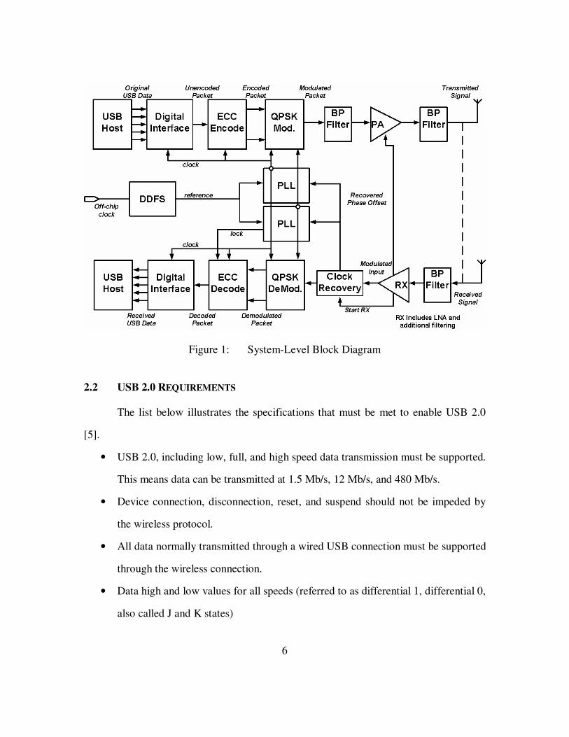
components in this system has its own requirements. Figure 1 details some of the major
sub-blocks of this system. The USB interface is represented by the host controller. The
transceiver contains the digital interface, the error correction blocks, and QPSK blocks.
The clocking block consists of the clock recovery, direct digital frequency synthesizer,
and the phase-locked loops. The wireless block consists of the two power and low noise
amplifiers, filters, and the antenna. The bulleted lists below mention the requirements
briefly, and they will be expanded upon later.
6
Figure 1: System-Level Block Diagram
2.2 USB 2.0 REQUIREMENTS
The list below illustrates the specifications that must be met to enable USB 2.0
[5].
• USB 2.0, including low, full, and high speed data transmission must be supported.
This means data can be transmitted at 1.5 Mb/s, 12 Mb/s, and 480 Mb/s.
• Device connection, disconnection, reset, and suspend should not be impeded by
the wireless protocol.
• All data normally transmitted through a wired USB connection must be supported
through the wireless connection.
• Data high and low values for all speeds (referred to as differential 1, differential 0,
also called J and K states)
7
• Single-ended zero values for all speeds which are used to indicate a reset
condition.
• Chirp J and Chirp K states utilized during reset to reset devices into the high
speed mode
• Squelching of invalid data when in high speed mode
• Device disconnection in high speed mode
• Total delay from USB transmit to USB receive (through the wireless protocol)
cannot exceed the maximum allowable USB cable delay of 30nanoseconds
• Total current consumption of wireless transceiver plus the attached function
controller cannot exceed a current of 200mA drawn from the USB controller.
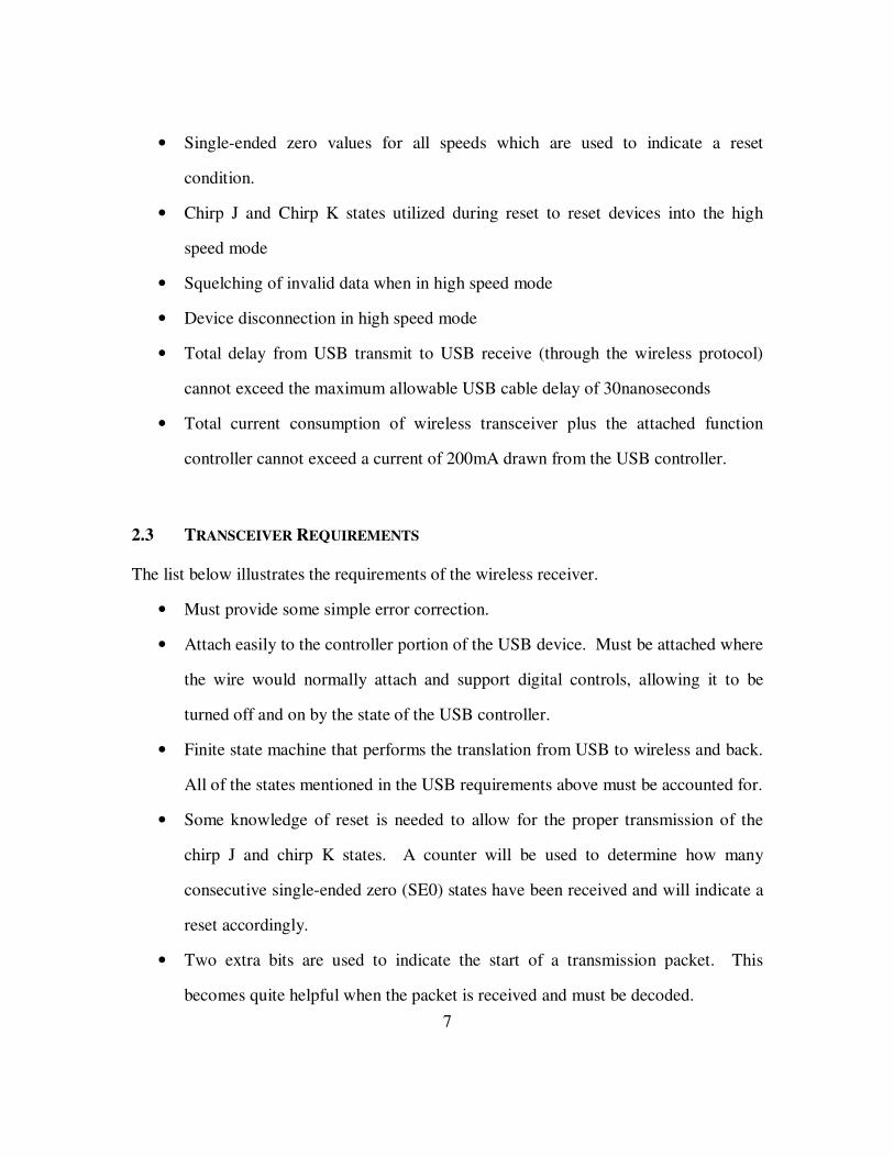
2.3 TRANSCEIVER REQUIREMENTS
The list below illustrates the requirements of the wireless receiver.
• Must provide some simple error correction.
• Attach easily to the controller portion of the USB device. Must be attached where
the wire would normally attach and support digital controls, allowing it to be
turned off and on by the state of the USB controller.
• Finite state machine that performs the translation from USB to wireless and back.
All of the states mentioned in the USB requirements above must be accounted for.
• Some knowledge of reset is needed to allow for the proper transmission of the
chirp J and chirp K states. A counter will be used to determine how many
consecutive single-ended zero (SE0) states have been received and will indicate a
reset accordingly.
• Two extra bits are used to indicate the start of a transmission packet. This
becomes quite helpful when the packet is received and must be decoded.
8
• Should take care of switching between full speed and high speed transmission
rates. Low speed devices cannot connect as high speed devices but high speed
devices need to connect as full speed before indicating it can utilize high speed
data rates.
2.4 CLOCKING AND WIRELESS REQUIREMENTS
The list below illustrates the clocking and carrier frequency requirements.
• Must support clock synchronization through the wireless channel
• Need to support 1.5 Mb/s 12 Mb/s, and 480 Mb/s transmission rates, as well the
wireless carrier wave, ideally 3.6 GHz.
• If utilizing current state transmission and start/end of packet transmission, clock
speeds of 3 times the various transmission rates must be supported/generated.
• Use some sort of digital frequency synthesis for carrier frequency generation.
Otherwise, use a PLL or off-chip crystal to generate the carrier frequency.
2.5 USB INTERFACE
The USB interface shown in Figure 2 below is taken from the USB 2.0
specification [5] and it was the starting point for interfacing the transceiver with USB.
The transceiver design basically removes the wire and the various resistors, but still has
to look functionally similar to the USB host controller. The USB signals that must be
accounted for are below the figure, and these signals must be accounted for in the
wireless transceiver.
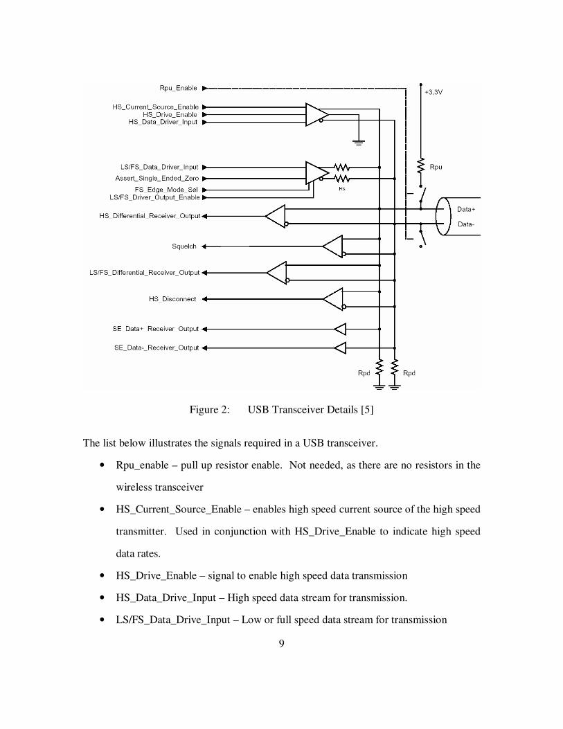
9
Figure 2: USB Transceiver Details [5]
The list below illustrates the signals required in a USB transceiver.
• Rpu_enable – pull up resistor enable. Not needed, as there are no resistors in the
wireless transceiver
• HS_Current_Source_Enable – enables high speed current source of the high speed
transmitter. Used in conjunction with HS_Drive_Enable to indicate high speed
data rates.
• HS_Drive_Enable – signal to enable high speed data transmission
• HS_Data_Drive_Input – High speed data stream for transmission.
• LS/FS_Data_Drive_Input – Low or full speed data stream for transmission
10
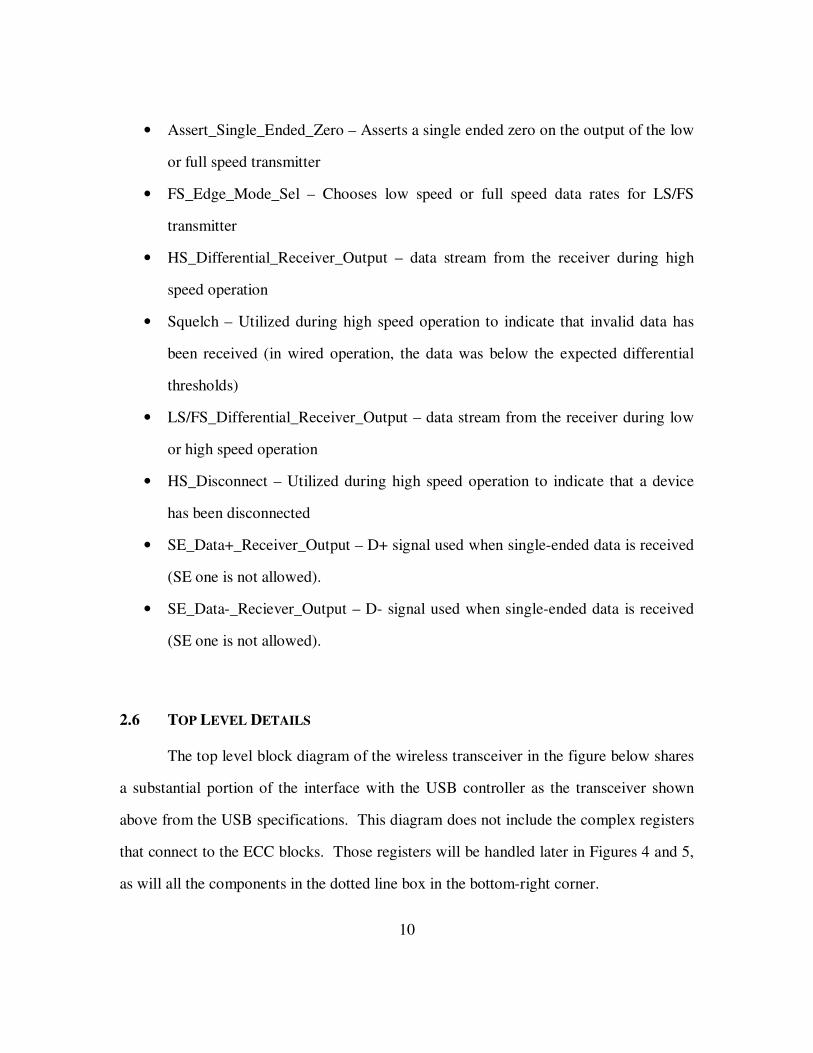
• Assert_Single_Ended_Zero – Asserts a single ended zero on the output of the low
or full speed transmitter
• FS_Edge_Mode_Sel – Chooses low speed or full speed data rates for LS/FS
transmitter
• HS_Differential_Receiver_Output – data stream from the receiver during high
speed operation
• Squelch – Utilized during high speed operation to indicate that invalid data has
been received (in wired operation, the data was below the expected differential
thresholds)
• LS/FS_Differential_Receiver_Output – data stream from the receiver during low
or high speed operation
• HS_Disconnect – Utilized during high speed operation to indicate that a device
has been disconnected
• SE_Data+_Receiver_Output – D+ signal used when single-ended data is received
(SE one is not allowed).
• SE_Data-_Reciever_Output – D- signal used when single-ended data is received
(SE one is not allowed).
2.6 TOP LEVEL DETAILS
The top level block diagram of the wireless transceiver in the figure below shares
a substantial portion of the interface with the USB controller as the transceiver shown
above from the USB specifications. This diagram does not include the complex registers
that connect to the ECC blocks. Those registers will be handled later in Figures 4 and 5,
as will all the components in the dotted line box in the bottom-right corner.
11
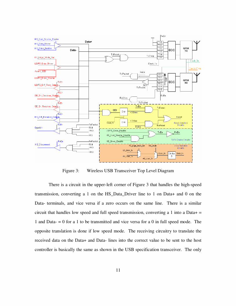
Figure 3: Wireless USB Transceiver Top Level Diagram
There is a circuit in the upper-left corner of Figure 3 that handles the high-speed
transmission, converting a 1 on the HS_Data_Driver line to 1 on Data+ and 0 on the
Data- terminals, and vice versa if a zero occurs on the same line. There is a similar
circuit that handles low speed and full speed transmission, converting a 1 into a Data+ =
1 and Data- = 0 for a 1 to be transmitted and vice versa for a 0 in full speed mode. The
opposite translation is done if low speed mode. The receiving circuitry to translate the
received data on the Data+ and Data- lines into the correct value to be sent to the host
controller is basically the same as shown in the USB specification transceiver. The only
12
addition is the RxEn gating signal that enables the output of the receiving circuitry only
when a valid packet reception has occurred.
There are a number of signals in the wireless transceiver that are not in the USB
specification transceiver.
• RxEn – Indicates that the receiver and receiver buffer should be enabled. This
occurs when none of the transmitter drivers are enabled by the USB controller.
• TxEn – Indicates that the transmitter and transmission buffer should be enabled.
This occurs when the USB controller indicates that either the HS or LS/FS driver
should be enabled. This also causes deactivation of the receiving circuitry.
• TxReset – Detects a reset state during transmission of 3.0 ms or more of state
SE0. Note that the counters that indicate the duration must have knowledge of the
current transmission speed to accurately detect this 3.0 ms.
• RxReset – Detects a reset state during reception of 2.5 us or more of SE0
• Reset – Indicates a reset state (either transmit reset or receive reset)
• LS_Clock_3x – Clock running at 3x the speed of LS transmission (4.5 MHz)
• FS_Clock_3x – Clock running at 3x the speed of FS transmission (36 MHz)
• HS_Clock_3x – Clock running at 3x the speed of HS transmission (1.44 GHz)
• Clock_3x – Clock running at 3x the speed of the current USB mode clock. This
is chosen based on what speed the USB controller is transmitting with.
• Clock_1x – Clock running at the speed of the current USB mode clock. This is
derived from the Clock_3x signal using a divide by 3 clock divider.
• TxChirp – Indicates that the J or K state being sent is actually a chirp signal, as
the device is in reset.
• RxChirp – Indicates that a chirp has been detected.
13
• RxPacket – Indicates that a packet has been successfully received, due to the
presence of a 1 in both the RX0 and RX1 flops in addition to the receiver being
enabled due to the assertion of RxEn.
Many of the signals in the transceiver are dependent upon the states being
transmitted or received. There are numerous states possible in the USB 2.0 architecture.
In low speed and full speed, there are 2 main states, the J and K state, which correspond
to either 01 or 10 on the Data+ and Data- lines. There is also a single-ended zero state
(SE0), which is denoted by zeros on both data lines. The high-speed state also has J, K,
and SE0 states. Since there are 3 main states for all transmission modes, it makes sense
to use 2 bits to denote the state transmitted. However, the high-speed mode also has
some extraneous states that are possible. When coming out of reset in high speed mode,
the host controller will broadcast chirp J and chirp K states, which in a wired solution
have a larger voltage swing than normal, but in the wireless solution will require an extra
bit to be sent, indicating that the device is chirping. Also in the high-speed state, the
transceiver must also indicate that data was being squelched, or that a device is
disconnecting. Between chirping, squelch, and disconnect, there are an additional three
states that must be accounted for.
To allow for error correction to work without increasing the clock frequency, six
USB transmissions are buffered together before transmission. This means that there are
twelve bits of USB data that need to be transmitted in each packet. To account for the
squelch, disconnect and chirp states, it would seem that there should be an additional 12
bits transmitted to indicate whether any of these states occurred during the transmission
of the USB data. However, since these states are all persistent states, meaning they most
likely occurred for a long string of USB states, only two bits are sent. If a squelch,
14
disconnect, or chirp occurred in any of the six USB transmissions, these bits are set
appropriately. Therefore, each packet will consist of sixteen bits: two header bits to
indicate start of transmission, twelve USB data information bits, and two chirp,
squelch/disconnect bits. The header consists of two consecutive ones, and the rest of the
bits are guaranteed to never repeat that sequence (once the data stream is partitioned for
QPSK modulation). This feature is to help the receiver realize when the start of a packet
occurs.
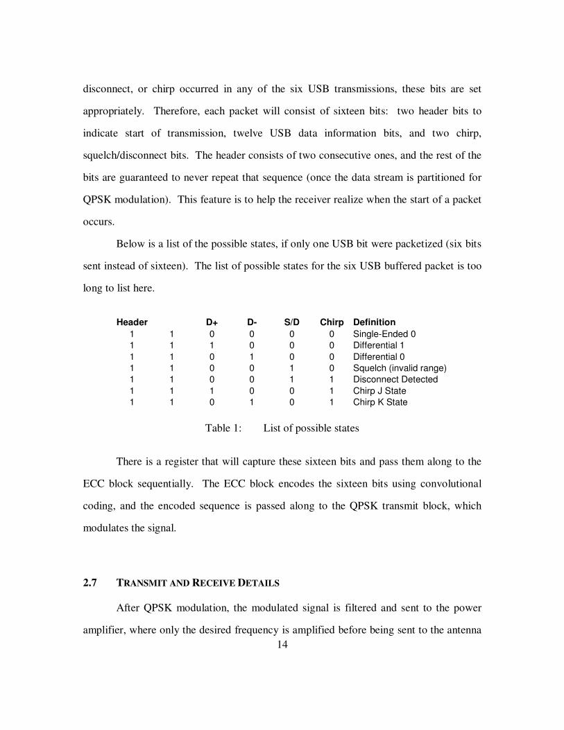
Below is a list of the possible states, if only one USB bit were packetized (six bits
sent instead of sixteen). The list of possible states for the six USB buffered packet is too
long to list here.
Header D+ D- S/D Chirp Definition
1 1 0 0 0 0 Single-Ended 01 1 1 0 0 0 Differential 11 1 0 1 0 0 Differential 01 1 0 0 1 0 Squelch (invalid range)1 1 0 0 1 1 Disconnect Detected1 1 1 0 0 1 Chirp J State1 1 0 1 0 1 Chirp K State
Table 1: List of possible states
There is a register that will capture these sixteen bits and pass them along to the
ECC block sequentially. The ECC block encodes the sixteen bits using convolutional
coding, and the encoded sequence is passed along to the QPSK transmit block, which
modulates the signal.
2.7 TRANSMIT AND RECEIVE DETAILS
After QPSK modulation, the modulated signal is filtered and sent to the power
amplifier, where only the desired frequency is amplified before being sent to the antenna

15
for transmission. On the receiving side, the encoded packet will pass through a filter, a
low noise amplifier, and then pass through the QPSK demodulator, which passes the
received sequence on to the ECC decoder (Viterbi decoder). The Viterbi decoder will
reconstruct the original packet from the received packet. When the packet is received,
the various bits will be used to create the RxPacket, squelch, disconnect, and data signals,
which will be passed on to the USB controller on the receive side.
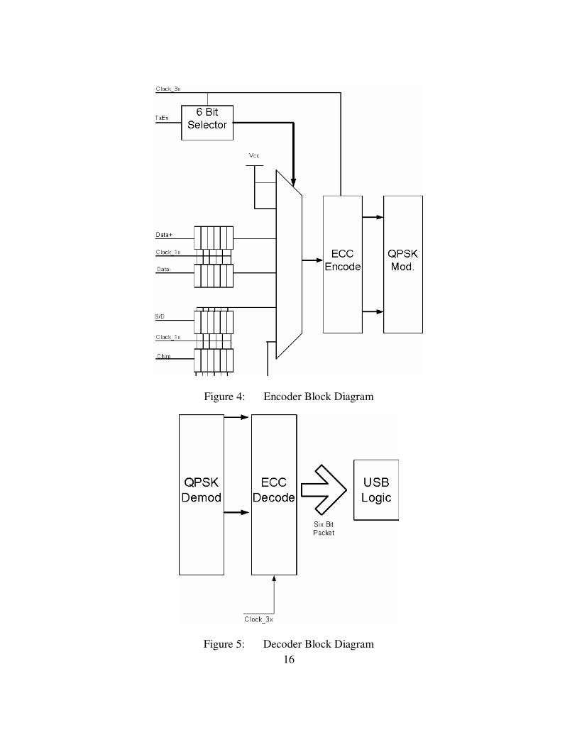
Figure 4 focuses on the register shown in the top-level diagram that precedes the
ECC block on the transmit path. This register packetizes the data that needs to be
encoded. There are four six-bit shift registers that capture the information on the Data+,
Data-, S/D, and Chirp lines on the 1x clock. These registers are enabled only when the
device is transmitting, and the various clocks will be discussed later. The outputs of the
data shift registers are fed sequentially to two inputs of a six-input multiplexor. The
logical OR of the outputs of the S/D shift register is sent to another input of the six-input
multiplexor, as is the logical OR of the outputs of the Chirp shift register. The final two
bits of the six-input multiplexor are tied to logic one, and represent the start of packet
information.
There is a small state machine that iterates through which multiplexor input drives
the output to the ECC encoder. This state machine is triggered on rising edges of the 3x
clock, ensuring all eighteen bits (sixteen data bits and two flush bits) are encoded in six
1x clock cycles. The eighteen bit input packet is encoded into a 36 bit packet. The
encoder also partitions the data into two data streams of 18 bits that are sent into the I and
Q inputs of the QPSK modulator.
16
Figure 4: Encoder Block Diagram
Figure 5: Decoder Block Diagram

17
On the receive side, the two outputs of the QPSK demodulator are sent straight to
the Viterbi decoder on the 3x clock. The Viterbi decoder takes these two 18-bit
sequences and decodes them into a single 16-bit sequence that contains all of the original
data. It then sends this data to the USB logic in packets of six bits that look like those
shown in Table 1. Not shown in Figure 5 are the filter and LNA that precede the
demodulator, nor the details of the Viterbi decoder, which is covered later.
2.8 CLOCKING DETAILS
Figure 6: Clock Selection Circuitry
USB 2.0 requires support of three different data speeds: 1.5 Mb/s, 12 Mb/s, and
480 Mb/s (Compaq). For purposes of this project, these are defined as the 1x clocks.
The transmit and receive registers as well as the ECC blocks require a clock that is three
times this frequency. All of these clocks are generated off of the same, high frequency
clock that is synthesized by a phase-locked loop, or PLL. This PLL clock is then divided
down to the 3 possible 3x clock frequencies (4.5 MHz, 36 MHz, and 1.44 GHz). As
portrayed in Figure 6, one system level 3x clock is chosen depending on the mode of
operation, and this system level 3x clock is passed through a divide by three circuit that
creates the system level 1x clock, which is the same speed as the USB data rate.
18
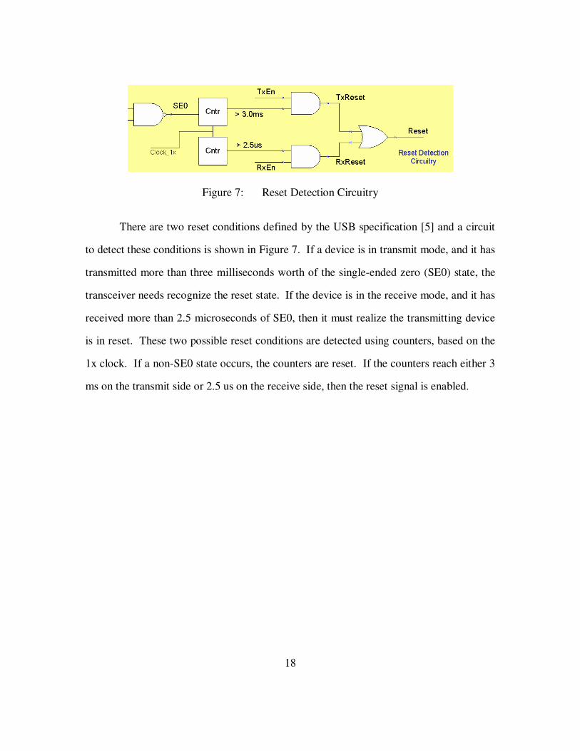
Figure 7: Reset Detection Circuitry
There are two reset conditions defined by the USB specification [5] and a circuit
to detect these conditions is shown in Figure 7. If a device is in transmit mode, and it has
transmitted more than three milliseconds worth of the single-ended zero (SE0) state, the
transceiver needs recognize the reset state. If the device is in the receive mode, and it has
received more than 2.5 microseconds of SE0, then it must realize the transmitting device
is in reset. These two possible reset conditions are detected using counters, based on the
1x clock. If a non-SE0 state occurs, the counters are reset. If the counters reach either 3
ms on the transmit side or 2.5 us on the receive side, then the reset signal is enabled.
19
Chapter 3: Error Correction
3.1 INTRODUCTION
In the realm of wireless communications, one of the most difficult challenges is
minimizing the effects of noise throughout the solution. Noise can be contributed in
many aspects of a design; from thermal noise to channel noise to interference to multi-
path and others. There are various ways to minimize the effects of these noise sources,
including the use of carefully designed low noise amplifiers to limit the noise to only a
small region around the desired frequency of operation as well as transmitting numerous
carrier frequency periods per transmitted bit. One other common feature to prevent these
errors is the use of error-correcting codes (ECC), with one of the most common ECCs
being convolutional coding with Viterbi decoding.
Convolutional codes generate some n number of output bits, based on a stream of
k input bits. The n output bits are generated from a combination of the current k input
bits and L previous sets of input bits. L is referred to as the constraint length, and it
represents how many time steps of inputs are convolved. For example, if the constraint
length is three, and the number of input bits per time step is two (k = 2), the number of
bits that need to be saved is four. The bits that combine to produce the output bits in this
case are the two current bits, the two bits from the previous time step, and the two bits
from two time steps previous. Convolutional coding schemes are generally referred to as
k/n codes. If the number of output bits generated in the example above is three, the code
would be referred to as a 2/3 code, as there are three output bits generated per two input
bits.
20
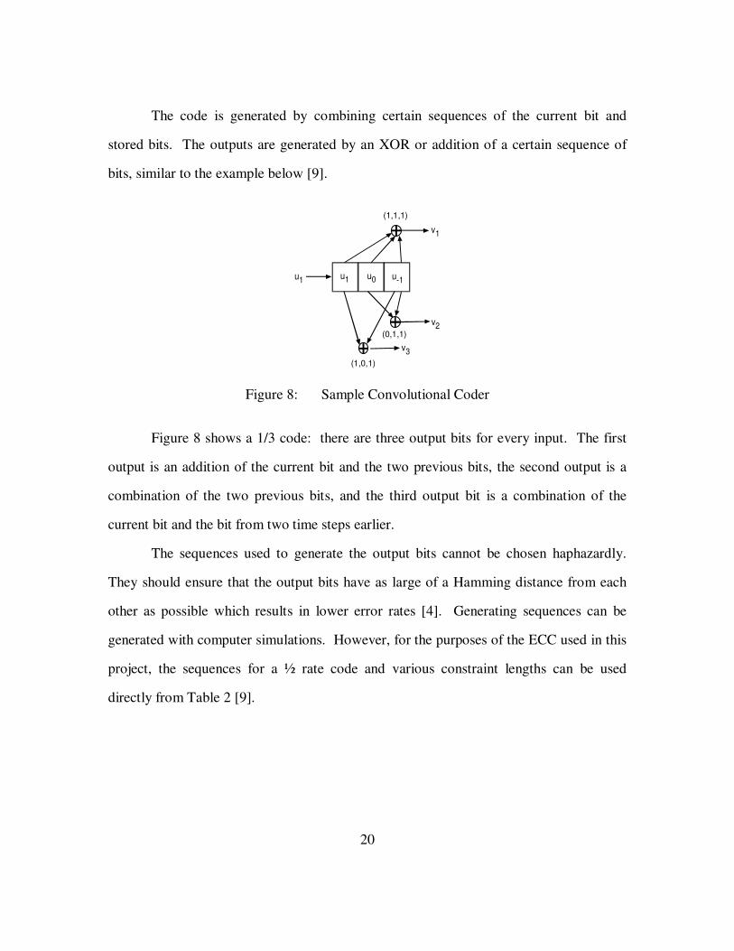
The code is generated by combining certain sequences of the current bit and
stored bits. The outputs are generated by an XOR or addition of a certain sequence of
bits, similar to the example below [9].
u1
v1
v2
u1 u0 u-1
v3
(1,1,1)
(1,0,1)
(0,1,1)
Figure 8: Sample Convolutional Coder
Figure 8 shows a 1/3 code: there are three output bits for every input. The first
output is an addition of the current bit and the two previous bits, the second output is a
combination of the two previous bits, and the third output bit is a combination of the
current bit and the bit from two time steps earlier.
The sequences used to generate the output bits cannot be chosen haphazardly.
They should ensure that the output bits have as large of a Hamming distance from each
other as possible which results in lower error rates [4]. Generating sequences can be
generated with computer simulations. However, for the purposes of the ECC used in this
project, the sequences for a ½ rate code and various constraint lengths can be used
directly from Table 2 [9].
21
Constraint Length G1 G23 110 1114 1101 11105 11010 111016 110101 111011
Table 2: Convolutional Codes for Various Constraint Lengths
Once generator sequences are chosen, it is easy to create a state diagram (also
referred to as a “trellis diagram”) to illustrate how the inputs are translated into the
outputs. The key idea is that every possible input sequence encodes into a unique set of
outputs, and all possible output sequences will differ from each other in as many bits as
possible.
There are a couple of ways to decode convolutionally encoded data. One option
is to use sequential decoding, where the bits are compared against possible states as they
are received. If the received bits differ from what is possible during the sequence, a state
machine will increment the number of errors received and makes a choice as to what the
input bits most likely were. It continues in this fashion until either it reaches the end of
what is received or until a certain threshold of errors is reached. If there are too many
errors, the decoder backtracks until it finds a path that minimizes the number of errors
when compared to possible sequences [9]. However, the problem with this decoding
technique stems from how long it takes. If the decision making in the face of an error is
poor, there can be lots of backtracking, which can take a lot of time. If the number of
errors allowed before backtracking is small, it leaves the door open for higher error rates.
Therefore, another method of decoding, called maximum likelihood decoding (one flavor
of which is Viterbi decoding) will be used.
Viterbi decoding examines the entire received sequence, possibly chopping it into
smaller pieces first, computing how much in common each received piece is in
22
comparison with all the valid sequences [4]. Possible received paths each have some
metric assigned to them, usually using the Hamming metric, showing how close to valid
paths the possible paths are. As each bit is received, the possible paths increase in length,
and each new path is updated with a new path metric. The number of possible paths can
quickly balloon to large values, but the list is continually pruned. At each state of the
decoder, many paths start to overlap, and only the ones that are closest to valid paths are
retained in each stage. Therefore, the total number of paths kept at any one time is the
same as the number of states in the encoder and decoder.
3.2 THE CONVOLUTIONAL CODER
Once deciding to use convolutional decoding, an appropriate rate code must be
chosen. Since multiple bits will need to be transmitted per USB transmission, and the
high-speed USB rate is 480 MHz, choosing a code with few output bits per input bit will
help keep the needed clock frequency at a reasonable level. Therefore, the desired code
will be a ½ code.
Now that a code rate has been settled upon, the choice of constraint lengths is
necessary. A constraint length of three requires only a few states and is pretty simple to
decode, but that alone is not enough reason to settle on a constraint length of three. Some
simulations were run on the Simulink setup shown in Figure 9, varying the constraint
length from three to six.

23
Figure 9: Simulink Viterbi Decoding Simulation
The results of the simulations are summarized in Table 3:
Constraint Length G1 G2 BER
3 110 111 0.006174 1101 1110 0.003235 11010 11101 0.004346 110101 111011 0.00061
Table 3: Simulation Viterbi Decoding Simulation Results
The channel used in this case essentially just adds white, Gaussian noise to the
input, and the modulation scheme used was BPSK. As the chart shows, using constraint
length of 3 provides a BER of 0.6%. It decreases going to four and six, although
interestingly, the length of five is actually higher than a constraint length of four. The
minimum BER occurs, not surprisingly, with a constraint length of six that proves a BER
of 0.06%. So, choosing a constraint length of three is not the best option, but still
provides a pretty viable alternative, as the project will actually be using QPSK, which
should cut the BER in half. The SNR in this case was 5 dB, so it was a pretty small
signal-to-noise ratio (probably more noise than the environment this device will be used
24
in). There are higher level protocols that could be used for retransmission should BER
prove problematic, although they are not included in this design.
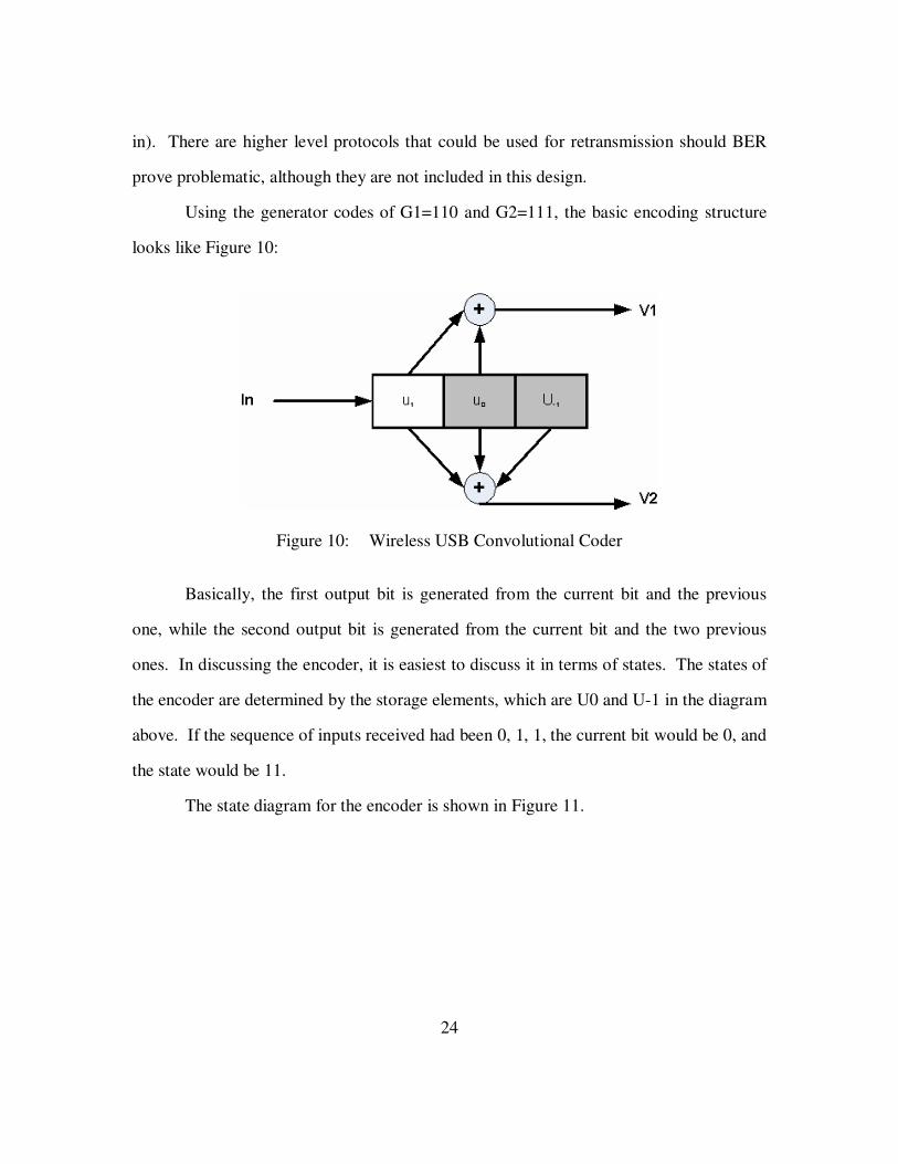
Using the generator codes of G1=110 and G2=111, the basic encoding structure
looks like Figure 10:
Figure 10: Wireless USB Convolutional Coder
Basically, the first output bit is generated from the current bit and the previous
one, while the second output bit is generated from the current bit and the two previous
ones. In discussing the encoder, it is easiest to discuss it in terms of states. The states of
the encoder are determined by the storage elements, which are U0 and U-1 in the diagram
above. If the sequence of inputs received had been 0, 1, 1, the current bit would be 0, and
the state would be 11.
The state diagram for the encoder is shown in Figure 11.
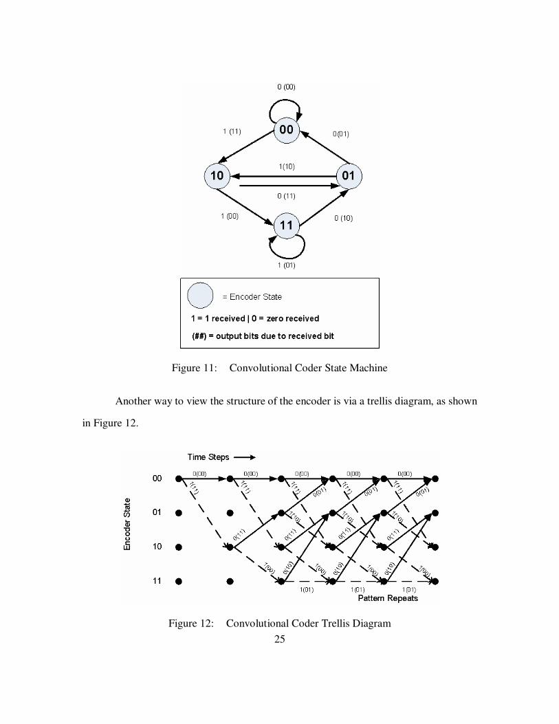
25
Figure 11: Convolutional Coder State Machine
Another way to view the structure of the encoder is via a trellis diagram, as shown
in Figure 12.
Figure 12: Convolutional Coder Trellis Diagram

26
The structure of the encoder ensures that the two outputs generated from each
input bit will differ in both bits: 11 vs. 00 or 01 vs. 10. This creates a greater Hamming
distance between the possible outputs, lowering the error rate [4].
Walking through either the state diagram beginning in state 00, if a 0 is received,
all of the stored bits and current bits are 0, so the output bits are 00: V1 = 0 + 0 + 0 and
V2 = 0 + 0 and the next state is state 00. Similarly, if a 1 is received while in state 00, the
output bits are 11: V1 = 1 + 0 + 0 and V2 = 1 + 0 and the next state is state 10. State 00
will always have the same behavior as mentioned above, so assuming a 1 is received, the
current state is 10. Now, if a 0 is received, the output bits are 11: V1 = 0 + 1 + 0 and V2
= 0 + 1, and the state machine progresses to state 01. However, if a 1 were received, the
output bits would be 00, as in modulo 2 arithmetic V1 = 1 + 1 + 0 = 0 and V2 = 1 + 1 = 0
and the state machine progresses to state 11. It should be easy to follow the trellis
diagram now, starting from state 00. The dotted lines indicate that a 1 was received while
in the current state while the solid lines indicate the input bit was 0. The text above the
lines show the bit received and, in parentheses, the corresponding output bits.
To show an example of encoding, the information in Table 1 will be used, even
though the actual packets will be 16 bits, not the 6 from the table. Although there are six
bits that are sent from the USB/logic interface per USB transmission, in reality there are
only nine possible values that this six bit packet could be. The first two bits will always
be ones, indicating the start of a packet, and the next two pairs have the limitation on
them that they cannot be all ones. The nine possible input packets and the encoded
outputs are shown in Table 4.
27
Valid Input Sequence
Encoded Output Flush Bits
110000 110010010000 0000110001 110010010011 1101110010 110010011111 0100110100 110010101101 0000110101 110010101110 1101110110 110010100010 0100111000 110001100100 0000111001 110001100111 1101111010 110001101011 0100
Table 4: Valid Encoding Outputs
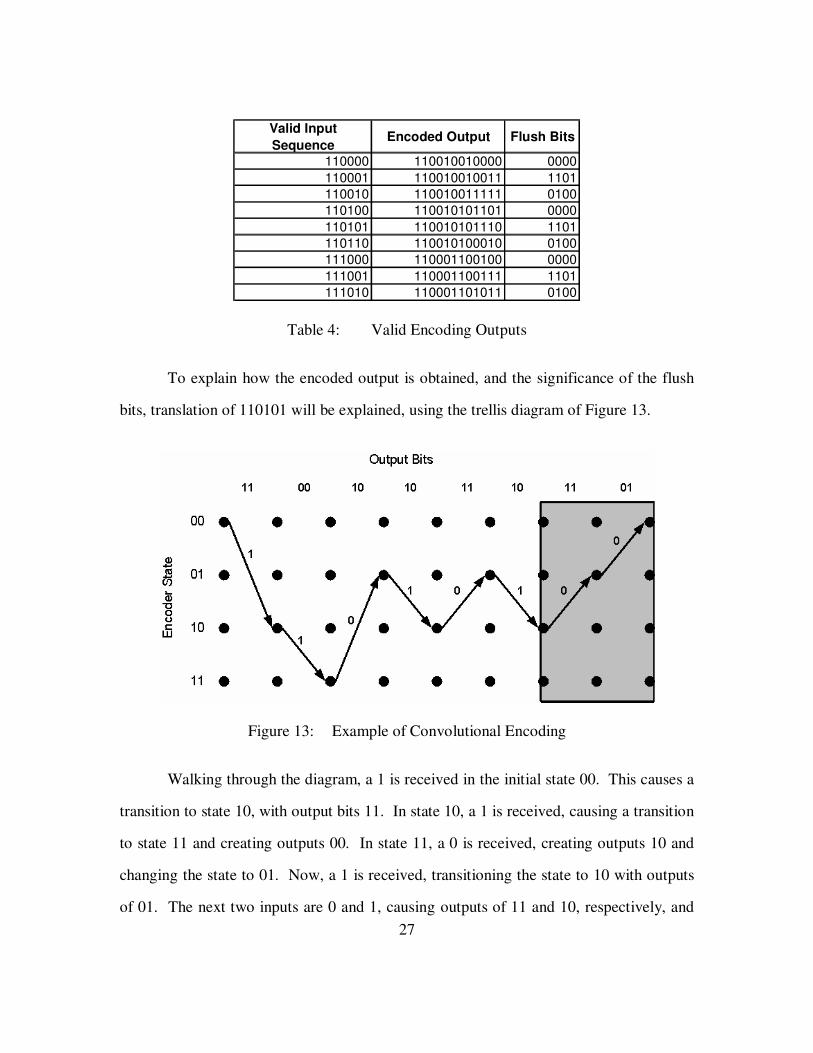
To explain how the encoded output is obtained, and the significance of the flush
bits, translation of 110101 will be explained, using the trellis diagram of Figure 13.
Figure 13: Example of Convolutional Encoding
Walking through the diagram, a 1 is received in the initial state 00. This causes a
transition to state 10, with output bits 11. In state 10, a 1 is received, causing a transition
to state 11 and creating outputs 00. In state 11, a 0 is received, creating outputs 10 and
changing the state to 01. Now, a 1 is received, transitioning the state to 10 with outputs
of 01. The next two inputs are 0 and 1, causing outputs of 11 and 10, respectively, and
28
the sequence has reached the grey box. So far, the input sequence 110101 has created
outputs of 110010101110, which matches the table above. The grey box represents the
outputs that are generated as the state machine is flushed. After the last input bit (a one
in this case) is received, it is moved into the state machine. To flush any residual data
from the packet from the state machine, 2 zeros are passed into the state machine. The
purpose of these zeros is to reset the state machine to state 00, but as each zero moves
through, they create more output bits [9].
Are these flush output bits worth transmitting, or should they just be discarded?
Well, in order to correct all patterns that contain n or fewer errors, each code must differ
from all other codes by greater than 2n+1 or more positions [4]. Without the flush bits,
the encoded outputs only differ from each other by 2 or more bits. That means that
without the flush bits, the encoding scheme cannot guarantee correcting ANY error, it
can only detect them. With the flush bits, all codes differ from each other by at least 4
bits, meaning that the scheme can guarantee to correct all single bit errors and detect all
double bit errors. These details are for hard-decision decoding, which uses absolute
voltage thresholds to determine the bit received. With soft-decision decoding, which uses
conditional probabilities depending on the magnitude of the voltage received and the
previous bit received [9] and is not used in this project, the scheme could come very close
to fixing most 2 bit errors. So, the flush bits are worth keeping around, even in the
project case, where 16 bits are already in each packet. In addition, by adding the 2 flush
bits, the total number of encoded bits to transmit jumps from 32 to 36, which is divisible
by three, and easily transmitted using the 3x clock.
29
3.3 THE VITERBI DECODER
At first glance, there are an overwhelming number of possible paths to compare
the input to. For the 36 bit packets that are transmitted, there would be 236 possible
packets (more than 68 billion possibilities). However, with the constraints that have been
put on the possible inputs to the encoder (the first 2 bits are always one, each USB packet
only has 3 states instead of 4, etc.), the number of valid packets is still 37, which is still
over 2000 valid packets. Comparing the values to these 2000+ valid packets could get
overwhelming very quickly. Fortunately, the Viterbi decoder is designed to avoid this
blowup. As each pair of bits is received, it prunes down the number of possible
sequences to one per encoder/decoder state: the most likely received packet per state [4].
Since there are only four possible encoder/decoder states in this solution, the decoder cuts
the 2000+ possible packets down to the four most likely received codes. Once the full
packet has been received, the decoder can quickly choose the most likely received packet
from these four possible packets and pass on the result to the rest of the receiver.
There are three main sub-blocks to the Viterbi decoder used in this project: the
path-decision block, the path and error updating block, and the path-output block. The
path-decision block is responsible for deciding what the two bits received from the QPSK
demodulator on every 3x clock cycle were supposed to be. It has a decision-making unit
for each state. For two bits, there are four possibilities for each QPSK output. However,
only two of those four represent a sequence that could put the state machine into a given
state. For example, from Figure 11, only states 00 and 01 could result in the next state
being state 00, and those transitions would have produced bit sequences of 00 or 01,
respectively. So, the decision-making unit of state 00 compares the two bit input to 00
and 01, and decides which one causes fewer errors. If the 00 sequence is more similar to
the received bits, it decides that state 00 was most likely the preceding state, so it shifts

30
the 00 values into the LSBs of the state 00 path register. If 01 is deemed more correct,
then state 01 was most likely the preceding state. Therefore, the path from state 01 is
shifted into the MSBs of state 00, while 01 is shifted into the LSBs. There is a similar
path-decision block for each of the four states. For state 01, it compares the input stream
to 10 and 11, for state 10 it compares it to 10 and 11, and for state 11 it compares it to 00
and 01. The registers are updated in a similar manner for all states as explained for state
00.
The path updating mentioned above takes place as part of the path and error
update block. Once the paths for each state have been updated, the errors must be
updated. The decoder already has computed how many errors occurred for the given two
bit input that is shifted into a state’s path, so it just adds that to the running total of errors
for that state. The other thing that happens in this block is on-the-fly decoding of the
input sequence according to a state’s current path. Since the decoder knows which state
the input sequence is coming from, and knows the bits, it can easily determine what the
input bit was that generated those bits. So, the decoded output for each state is computed
during path updating as well.
Finally, once the whole packet has been received, there are four paths from which
to choose the output; one from each state. The choice is made by comparing the error
totals that have accumulated for each state. Obviously, the one with the fewest errors is
chosen, and the decoded data that corresponds to the chose state is sent out in six bit
parcels to the receiver. The six bits consist of the header bits, the D+ and D- bits, and the
S/D and Chirp bits. The full 16 bits of original data is sent in six 1x clock cycles,
matching the speed at which it was created by the transmitter and encoder.
31
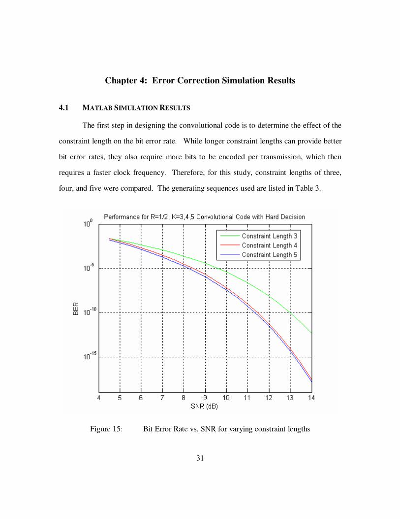
Chapter 4: Error Correction Simulation Results
4.1 MATLAB SIMULATION RESULTS
The first step in designing the convolutional code is to determine the effect of the
constraint length on the bit error rate. While longer constraint lengths can provide better
bit error rates, they also require more bits to be encoded per transmission, which then
requires a faster clock frequency. Therefore, for this study, constraint lengths of three,
four, and five were compared. The generating sequences used are listed in Table 3.
Figure 15: Bit Error Rate vs. SNR for varying constraint lengths
32
The bit error rate for lengths four and five are almost identical, while that of the
length three is a little worse. However, the benefits of the length three code supersedes
the fact that it has a little higher bit error rate. Using the length three code allows for a
slower clock speed, and allows for a simpler decoder, saving both power and area.
Besides, the error rate at high SNR values, most like the operating region of this device,
are still quite miniscule for the length three code.
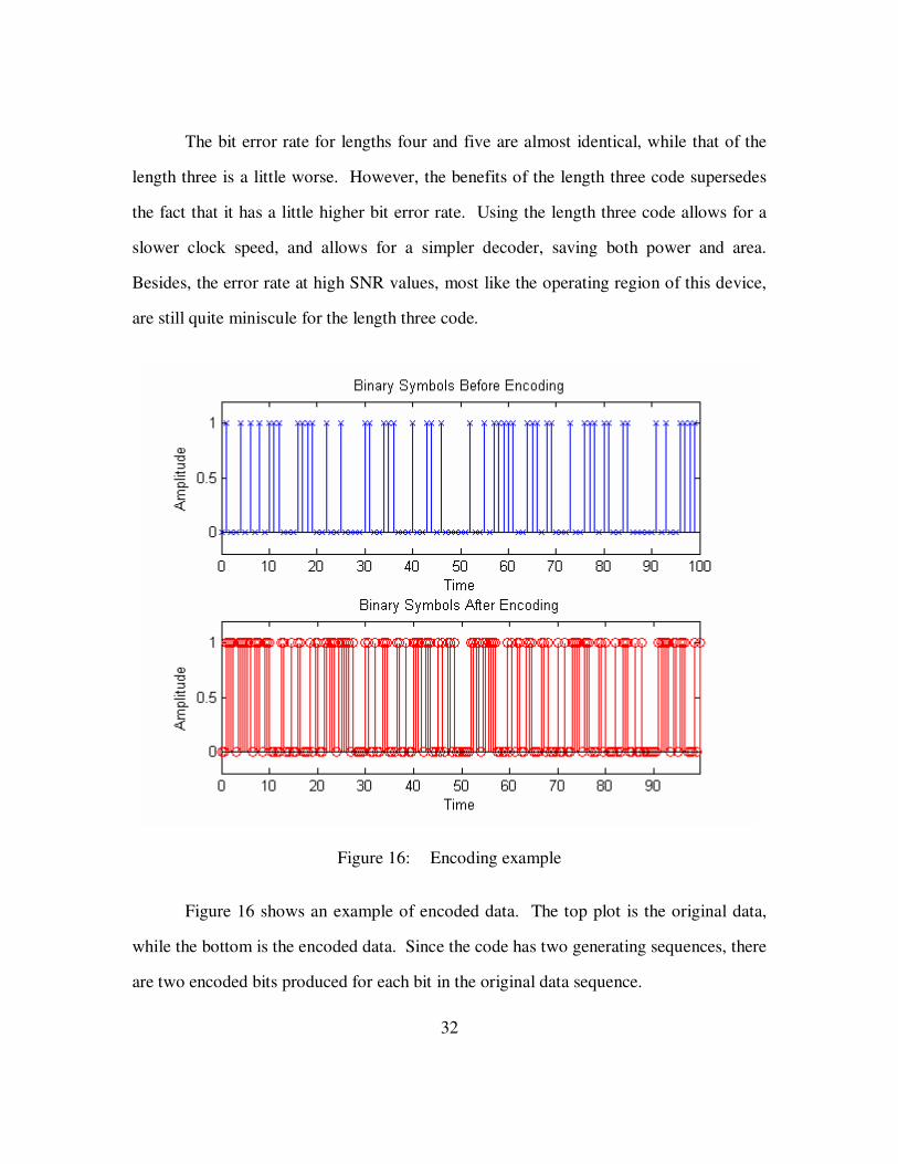
Figure 16: Encoding example
Figure 16 shows an example of encoded data. The top plot is the original data,
while the bottom is the encoded data. Since the code has two generating sequences, there
are two encoded bits produced for each bit in the original data sequence.
33
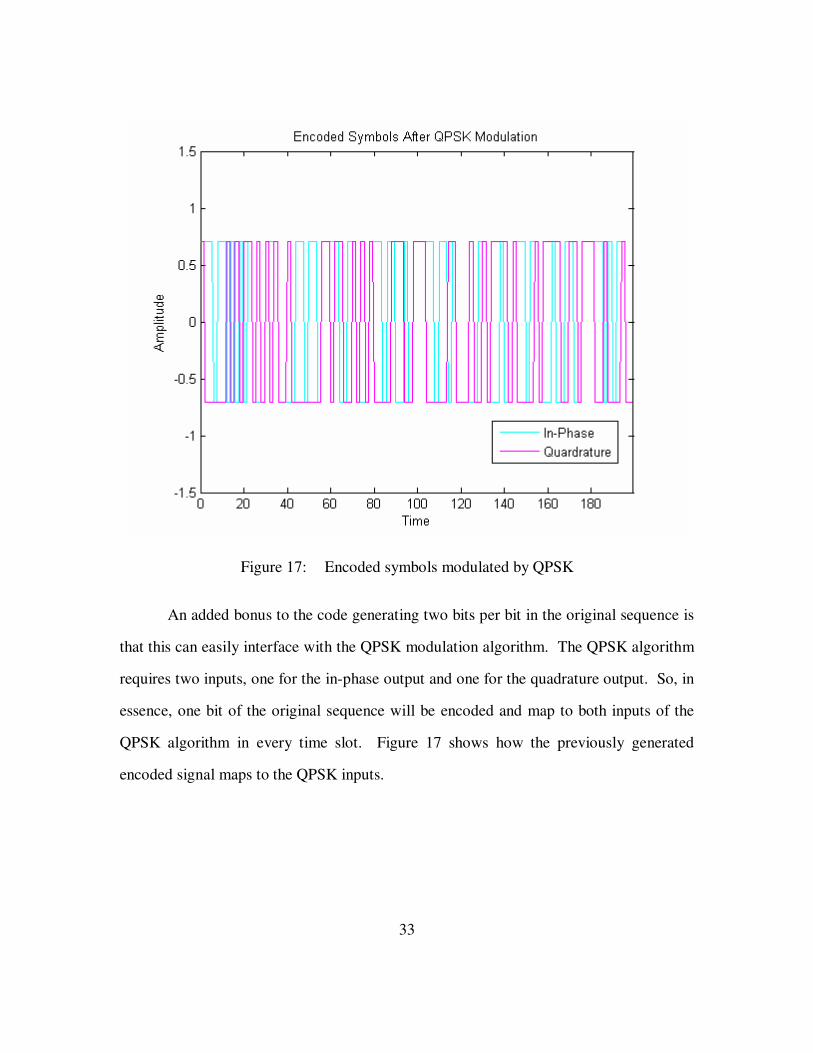
Figure 17: Encoded symbols modulated by QPSK
An added bonus to the code generating two bits per bit in the original sequence is
that this can easily interface with the QPSK modulation algorithm. The QPSK algorithm
requires two inputs, one for the in-phase output and one for the quadrature output. So, in
essence, one bit of the original sequence will be encoded and map to both inputs of the
QPSK algorithm in every time slot. Figure 17 shows how the previously generated
encoded signal maps to the QPSK inputs.

34
Figure 18: Transmitted vs. Received Data
The channel noise in these Matlab simulations is modeled as simple, white
Gaussian noise. Figure 18 shows the differences between the data that was transmitted
through the channel and the data that was received after the channel. Since such a short
time period is shown, a low SNR (5 dB in this case) was used to show what happens
when errors occur. The transmitted bits are marked by an ‘x’ , while the received are
marked by an ‘o’ . Three total errors occur in this sample: a single error at time 6, and
consecutive errors around time 43.
35
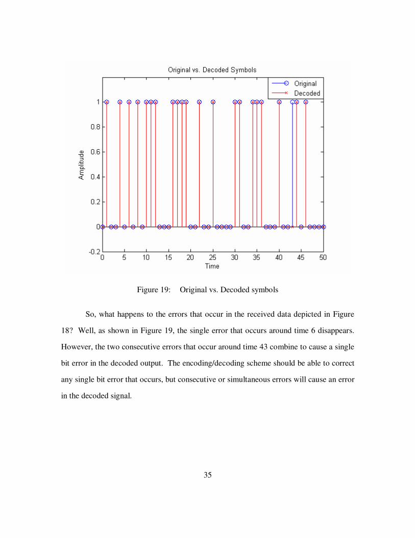
Figure 19: Original vs. Decoded symbols
So, what happens to the errors that occur in the received data depicted in Figure
18? Well, as shown in Figure 19, the single error that occurs around time 6 disappears.
However, the two consecutive errors that occur around time 43 combine to cause a single
bit error in the decoded output. The encoding/decoding scheme should be able to correct
any single bit error that occurs, but consecutive or simultaneous errors will cause an error
in the decoded signal.
36
4.2 VERILOG SIMULATION RESULTS
After defining the specifications for the encoder and decoder and then simulating
them in Matlab, they were ported to Verilog. The verification of the Verilog
implementation of the encoder/decoder pair was accomplished in three parts. First, the
encoder was coded and tested by first passing through a single packet of data, and then by
sending through a string of packets. Once the encoder was working, it was used to
generate encoded data streams for testing of the decoder. The inputs to the decoder were
connected directly to the outputs of the encoder. In similar fashion to the encoder, it was
tested by sending first a single packet through, and then a string of packets. This set of
tests could prove that data can be encoded and decoded, but does not test out the error
correction of the decoder. The data stream to the decoder contained no errors. To test
the error correction capabilities of the decoder, it was disconnected from the encoder.
The decoder then received inputs that were the same as the ones the encoder generated,
but some of the bits were flipped. Codes were sent through with a single bit error, then
with a couple widely-spaced bit errors, and then with consecutive bit errors. The results
from these tests are discussed here.
37
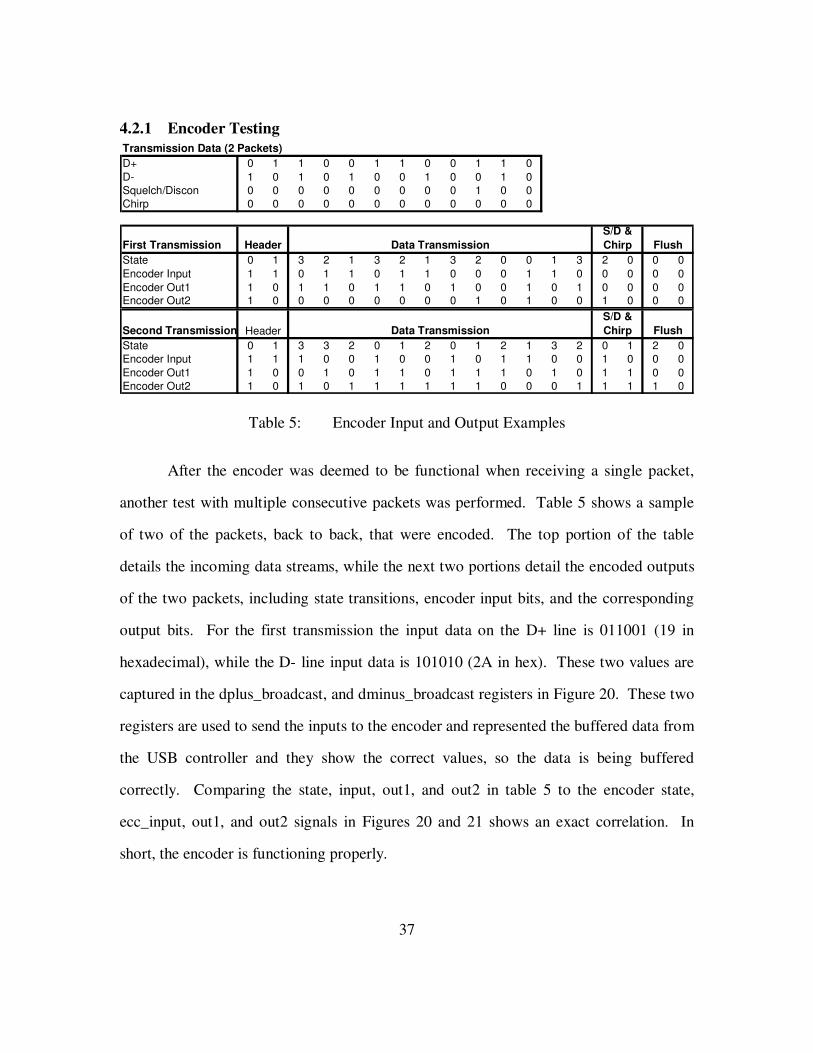
4.2.1 Encoder Testing Transmission Data (2 Packets)D+ 0 1 1 0 0 1 1 0 0 1 1 0D- 1 0 1 0 1 0 0 1 0 0 1 0Squelch/Discon 0 0 0 0 0 0 0 0 0 1 0 0Chirp 0 0 0 0 0 0 0 0 0 0 0 0
First TransmissionState 0 1 3 2 1 3 2 1 3 2 0 0 1 3 2 0 0 0Encoder Input 1 1 0 1 1 0 1 1 0 0 0 1 1 0 0 0 0 0Encoder Out1 1 0 1 1 0 1 1 0 1 0 0 1 0 1 0 0 0 0Encoder Out2 1 0 0 0 0 0 0 0 0 1 0 1 0 0 1 0 0 0
FlushS/D & ChirpData TransmissionHeader
Second TransmissionState 0 1 3 3 2 0 1 2 0 1 2 1 3 2 0 1 2 0Encoder Input 1 1 1 0 0 1 0 0 1 0 1 1 0 0 1 0 0 0Encoder Out1 1 0 0 1 0 1 1 0 1 1 1 0 1 0 1 1 0 0Encoder Out2 1 0 1 0 1 1 1 1 1 1 0 0 0 1 1 1 1 0
Data TransmissionHeaderS/D & Chirp Flush
Table 5: Encoder Input and Output Examples
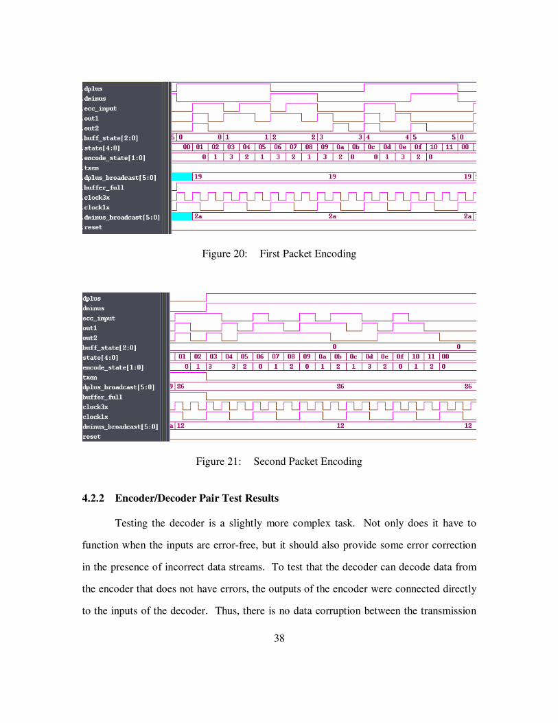
After the encoder was deemed to be functional when receiving a single packet,
another test with multiple consecutive packets was performed. Table 5 shows a sample
of two of the packets, back to back, that were encoded. The top portion of the table
details the incoming data streams, while the next two portions detail the encoded outputs
of the two packets, including state transitions, encoder input bits, and the corresponding
output bits. For the first transmission the input data on the D+ line is 011001 (19 in
hexadecimal), while the D- line input data is 101010 (2A in hex). These two values are
captured in the dplus_broadcast, and dminus_broadcast registers in Figure 20. These two
registers are used to send the inputs to the encoder and represented the buffered data from
the USB controller and they show the correct values, so the data is being buffered
correctly. Comparing the state, input, out1, and out2 in table 5 to the encoder state,
ecc_input, out1, and out2 signals in Figures 20 and 21 shows an exact correlation. In
short, the encoder is functioning properly.
38
Figure 20: First Packet Encoding
Figure 21: Second Packet Encoding
4.2.2 Encoder/Decoder Pair Test Results
Testing the decoder is a slightly more complex task. Not only does it have to
function when the inputs are error-free, but it should also provide some error correction
in the presence of incorrect data streams. To test that the decoder can decode data from
the encoder that does not have errors, the outputs of the encoder were connected directly
to the inputs of the decoder. Thus, there is no data corruption between the transmission

39
and reception. The same packets that are shown in Table 5 are the ones that are tracked
in Figures 22 and 23 below. The correct path can be followed through the various states
by looking at the state##_err signals. Since there is no noise, the correct path will have
no errors. So the err signal that has 00 for its value is the correct path as it passes through
the decoder. It starts at state 00 and moves to 10, 11, 01, etc. At the end of the packet
reception, when the packet_received signal goes high, the correct data is chosen from the
four state data options. In this case, the correct value is 36C60 (hex) and is residing in
state 00, which can be derived from the first transmission portion of table 5.
Figure 22: First Packet Decoding
The second packet that is decoded is the one from the second transmission portion
of Table 5. Similar to the previous figure, the correct path can be followed through the
decoder by following 00 as it traverses through the state##_err signals. In this case the
correct data to be captured is 392C8 which, again, can be computed from Table 5.
However, the other interesting thing shown in Figure 23 is the transmission of the data
from the previous packet to the rest of the receiver. It is represented by the rx[5:0] signal
below. The correct sequence of six six-bit packets to send for the 36C60 data that was
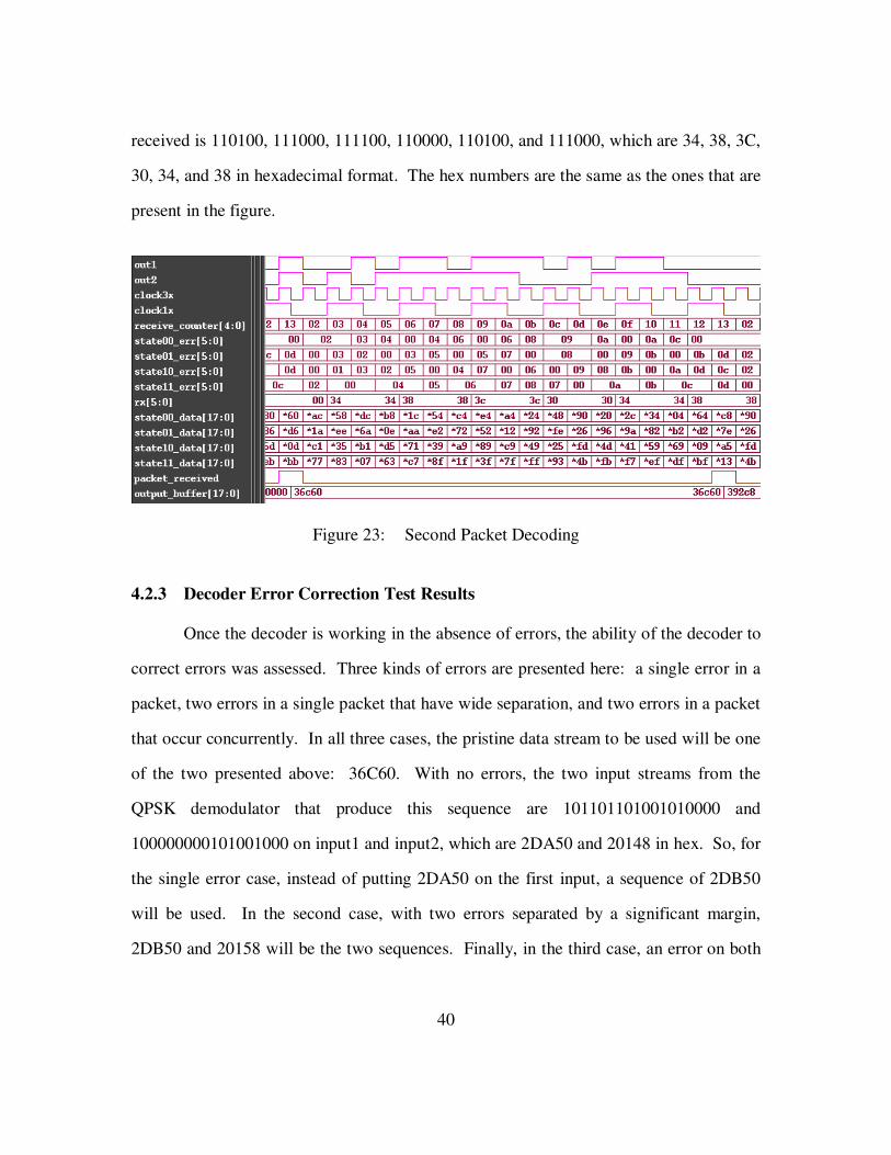
40
received is 110100, 111000, 111100, 110000, 110100, and 111000, which are 34, 38, 3C,
30, 34, and 38 in hexadecimal format. The hex numbers are the same as the ones that are
present in the figure.
Figure 23: Second Packet Decoding
4.2.3 Decoder Error Correction Test Results
Once the decoder is working in the absence of errors, the ability of the decoder to
correct errors was assessed. Three kinds of errors are presented here: a single error in a
packet, two errors in a single packet that have wide separation, and two errors in a packet
that occur concurrently. In all three cases, the pristine data stream to be used will be one
of the two presented above: 36C60. With no errors, the two input streams from the
QPSK demodulator that produce this sequence are 101101101001010000 and
100000000101001000 on input1 and input2, which are 2DA50 and 20148 in hex. So, for
the single error case, instead of putting 2DA50 on the first input, a sequence of 2DB50
will be used. In the second case, with two errors separated by a significant margin,
2DB50 and 20158 will be the two sequences. Finally, in the third case, an error on both
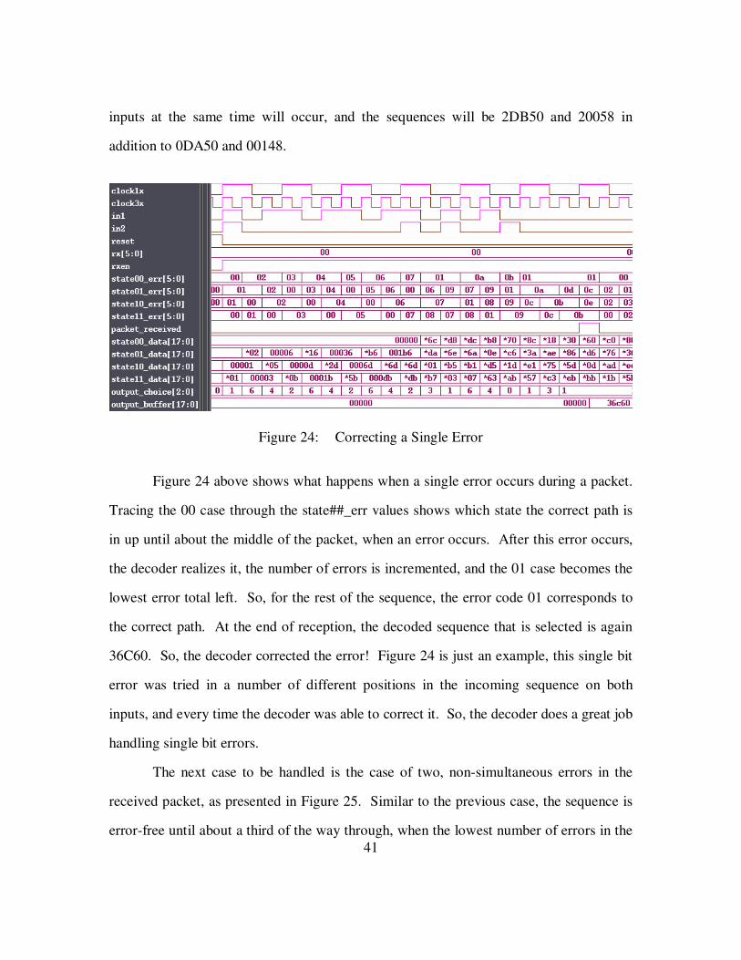
41
inputs at the same time will occur, and the sequences will be 2DB50 and 20058 in
addition to 0DA50 and 00148.
Figure 24: Correcting a Single Error
Figure 24 above shows what happens when a single error occurs during a packet.
Tracing the 00 case through the state##_err values shows which state the correct path is
in up until about the middle of the packet, when an error occurs. After this error occurs,
the decoder realizes it, the number of errors is incremented, and the 01 case becomes the
lowest error total left. So, for the rest of the sequence, the error code 01 corresponds to
the correct path. At the end of reception, the decoded sequence that is selected is again
36C60. So, the decoder corrected the error! Figure 24 is just an example, this single bit
error was tried in a number of different positions in the incoming sequence on both
inputs, and every time the decoder was able to correct it. So, the decoder does a great job
handling single bit errors.
The next case to be handled is the case of two, non-simultaneous errors in the
received packet, as presented in Figure 25. Similar to the previous case, the sequence is
error-free until about a third of the way through, when the lowest number of errors in the
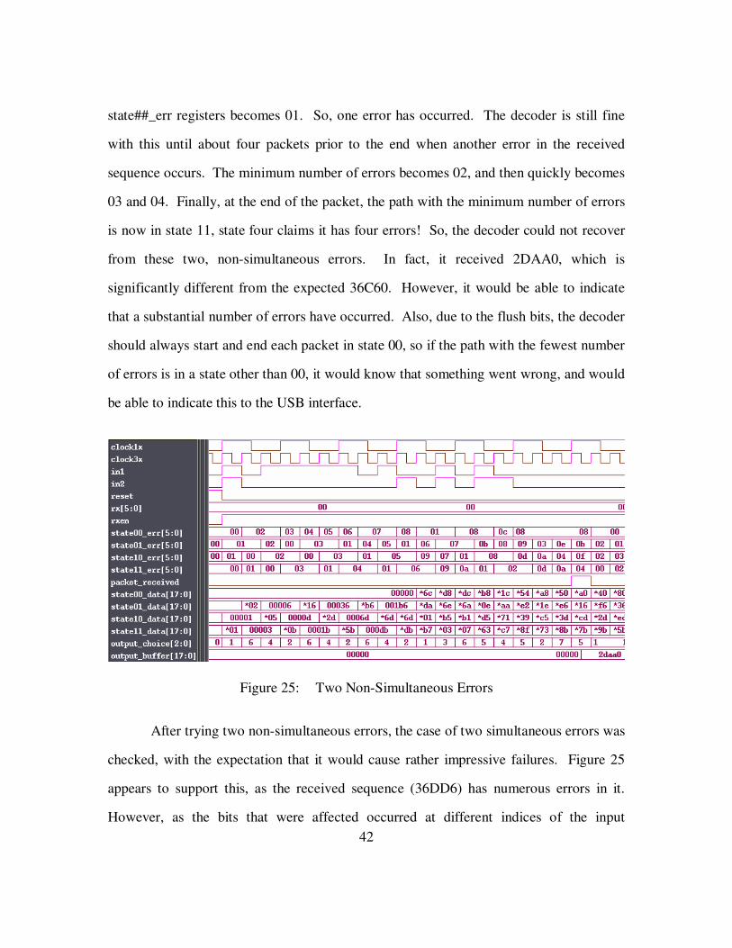
42
state##_err registers becomes 01. So, one error has occurred. The decoder is still fine
with this until about four packets prior to the end when another error in the received
sequence occurs. The minimum number of errors becomes 02, and then quickly becomes
03 and 04. Finally, at the end of the packet, the path with the minimum number of errors
is now in state 11, state four claims it has four errors! So, the decoder could not recover
from these two, non-simultaneous errors. In fact, it received 2DAA0, which is
significantly different from the expected 36C60. However, it would be able to indicate
that a substantial number of errors have occurred. Also, due to the flush bits, the decoder
should always start and end each packet in state 00, so if the path with the fewest number
of errors is in a state other than 00, it would know that something went wrong, and would
be able to indicate this to the USB interface.
Figure 25: Two Non-Simultaneous Errors
After trying two non-simultaneous errors, the case of two simultaneous errors was
checked, with the expectation that it would cause rather impressive failures. Figure 25
appears to support this, as the received sequence (36DD6) has numerous errors in it.
However, as the bits that were affected occurred at different indices of the input

43
sequence, the results changed. In some cases, such as shown in Figure 26 which had the
first bit of both input streams flipped, the decoder was still able to recover 36C60, which
was the original sequence. It also indicates that two errors occurred. In some cases, the
decoder is able to recover from 2 errors.
Figure 26: Correcting Two Simultaneous Errors
Figure 27: Two Simultaneous Errors That Are Not Correctable

44
4.2.4 Encoder/Decoder Summary
The encoder-decoder pair should be able to correct any single bit error that occurs
during the transmission of a packet. Also, it may be able to correct some two bit errors,
but will not be able to do so all the time. The decoder would know that errors have
occurred and, although not implemented in this project, could indicate to the host
controller that it could not correct the errors in the transmission, so the data could be
squelched or it could ask for retransmission. The single bit error correction is sufficient
for this project as the packets are small enough to avoid most bundles of errors. In order
to increase the number of bits to be corrected, a larger constraint length or a larger k value
would need to have been chosen for the encoder.
45
Chapter 5: Project Integration and Conclusion
A systematic approach has been presented for the design of a wireless USB
transceiver, from a problem statement to the realization of the low-power monolithic IC
design for a wireless USB transceiver. The first chapter goes through the overall design
problem and proposed solution; to replace the complex tangle of wiring used to connect
consumer electronics, computer peripheral, and mobile devices with a high-bandwidth
wireless, low-power, low-cost wireless links. The second chapter goes through high-level
details for the wireless USB device: how the transceiver communicates with the USB
physical interface, how the device is going to package the data for wireless
communication and obviously the wireless transmission itself. The USB wireless
transceiver would need to transmit 4 bits, to cover all the USB states. This would imply
that a packet of 6 bits, including headers, would be needed to transmit at USB data
speeds. However, to enable the use of error correction, six USB transmissions are
buffered together prior to encoder, and 18 bits are encoded into 36 bits for each wireless
packet. Since a QPSK transmission scheme was chosen for the USB Wireless Device,
which in effect doubles the data that can be transmitted, in essence 18 bits are sent during
the course of six USB transmissions, so three QPSK symbols per USB transmission.
Therefore, the data for high-speed USB would need to be transmitted at 1.44 GHz
(480Mb/sec*3). The frequency of the carrier waves to carry these data packets was set to
3.6 GHz.
The wireless USB project then diverged into the design of 4 major components
for the wireless USB design: 1) USB Interface, Packet Generation, and Error Correction
Scheme 2) Clock Recovery Mechanism between the Transmitter and Receiver [6] 3) low
noise amplifier (LNA), power amplifier (PA), and antenna [13] and 4) Frequency

46
Synthesizer for sine and cosine wave generation for the QPSK transmission scheme [8].
Emphasis was made on each of these major components to reduce the power dissipation
and area.
5.1 DIGITAL USB INTERFACE AND ERROR CORRECTION CIRCUITRY
A method to provide a simple interface with basic error correction between a USB
2.0 device and the QPSK wireless transmission algorithm has been presented. The
interface takes inputs from an attached USB host controller that are generated at a
maximum frequency of 480 MHz and creates buffers of six USB transmissions to be
encoded via a convolutional coder that employs a 1/3 rate code. The two outputs of the
convolutional coder are the inputs to the QPSK, which modulates the data, which is
generated with a maximum frequency of 1.44 GHz, with a 3.6 GHz carrier wave. On the
receiving end, the decoder receives two streams of data from the QPSK demodulator.
The decoder decodes the data using the Viterbi algorithm, eventually choosing the most-
likely received data from four sets of saved data. The selected data stream is then
broadcast to the receiving end of the USB interface in six bit parcels, which are generated
off the 1x clock which has a maximum frequency of 480 MHz. These parcels contain
two header bits, data + and data – bits, as well as the s/d and chirp bits. These are
converted inside the interface to the correct format and then sent on to the host controller.
The overall interface is quite simple from a digital circuit standpoint. It consists
mostly of small pieces of logic to do the data conversion and determine when a packet is
received or transmitted. The largest portion of it is the counters used to detect a reset
condition. To do this, there must be one counter that can detect 2.5 us of a certain state
and another that detects 3 ms of the state. These can be done with a 13-bit counter and a
47
2-bit counter, if the low speed 1x clock with a frequency of 1.5 MHz is used. In total, the
digital interface consumes about 1 mW of power during transmit or receive.
The transmit register is more complex than the top interface, but still rather
simple. It consists of 9 flip-flops running on the 3x clock (1.44 GHz), and 41 flip-flops
running on the 1x clock (480 MHz). It also contains 2 single bit precision adders to
perform the convolutional encoding. From simulations, this results in a power
consumption of 4.2 mW during transmit for the transmit register.
The receive register is the most complex portion of the digital interface. It
contains 253 flip-flops operating on the 3x clock which store the various paths, the
number of errors they contain, and the like. It also contains 11 flops that operate on the
1x clock and 18 flip-flops that essentially operate at 80 MHz which take care of the
interface between the top interface and the decoder. Finally, it contains five 6-bit adders
to update the number of errors found in the stored paths, and three 5-bit comparators to
decide with of the paths contain the fewest errors. From simulations, a power
consumption 63 mW is seen during reception in the receive register.
The encoder and decoder’ s primary interface is with the top level interface and
the QPSK modulator and demodulator as mentioned above. However, it also will not
perform any encoding nor decoding until it has received a signal from the clock recovery
mechanism that the PLL has locked.
5.2 CLOCK RECOVERY MECHANISM
The clock recovery scheme takes a very straight forward approach to solving this
problem. Using a QPSK transmit and receive scheme allows for the easy recovery of the
clock using standard analog integration techniques. By starting out with a receive clock
48
that is “close” to the same frequency that was transmitted, the clock recovery circuitry
can recover the data and the phase offset using integrators and mixers. The frame
recovery can also be realized using a standard integrator.
The phase offset recovered from the incoming wave can then be fed back to the
PLLs for use in helping the PLL to lock onto the transmitted frequency. There are two
PLLs used in this system, one to generate sine terms and one to generate cosine terms [6].
Each PLL receives a reference clock from the frequency synthesizer (One sine and one
cosine) that is used as a direct input into the phase detector. The phase detector then
compares the frequency and phase of the reference clock to the phase term generated by
the clock recovery circuitry and controls the VCO appropriately. The system requires a
start signal form the LNA circuitry that enables the PLL to start the locking sequence.
The transmitter will begin transmitting random data upon power up, so there will be
sufficient time to achieve lock.
Once the PLL has locked on frequency, the clock recovery circuitry will begin
transmitting data to the ECC block. Prior to that, the clock recovery circuitry will
transmit an enable signal to the ECC block letting it know that the incoming data stream
is valid and that the PLL is locked.
Since QPSK is fairly tolerant to jitter on the clock, the response time of the PLL is
not absolutely critical. This clock recovery mechanism will adjust to phase shifts every
cycle, but is limited by the response time of the PLL. Overall, the system will be able to
correct for phase shifts and large amounts of jitter while continuing to align to the frame
boundary [6].
49
5.3 LOW-NOISE AMPLIFIER, POWER AMPLIFIER, AND ANTENNA
The straightforward approach of the single ended low noise amplifier (LNA)
allowed for clean and simple input mechanism to receive the transmitted signal from the
antenna [13]. By using a single ended LNA, it was able to produce a signal output that
met the requirements for noise rejection as well as utilize a low power implementation.
The use of a direct down conversion scheme on the input architecture can keep the
number of off chip components to a minimum, continuing the trend of low power, low
cost implementation. The single ended LNA was critical to realizing these constraints.
The single ended LNA front end architecture consists of the antenna followed by
the off chip channel select bandpass filter. The signal gets received by the LNA on die
and further bandpass filtered to hone in on the fundamental 3.6 GHz signal. The main
mechanism through which the LNA achieves its gain at a given frequency while at the
same time attenuating other frequencies is tuned inductive resonance. The LNA tries to
minimize the amount of noise injected into the system at 3.6 GHz and minimize noise at
other frequencies. In that manner, it can achieve a very high signal to noise ratio with a
small, single stage of amplification. The overall LNA solution should also include sine
wave input detection circuitry to notify downstream components like the clock recovery
block that it is receiving a signal.
The power amplifier is essentially the reverse of the LNA. It tries to transmit a
given amount of power to the antenna at a desired frequency and not transmit at any other
frequencies. The necessity to deliver power to a load drives the amount of power
consumed. The design goals called for minimizing power consumed as well as off die
components needed. Again, the direct up conversion architecture enables the ease of
lowering component count helping us meet our constraints [13].
50
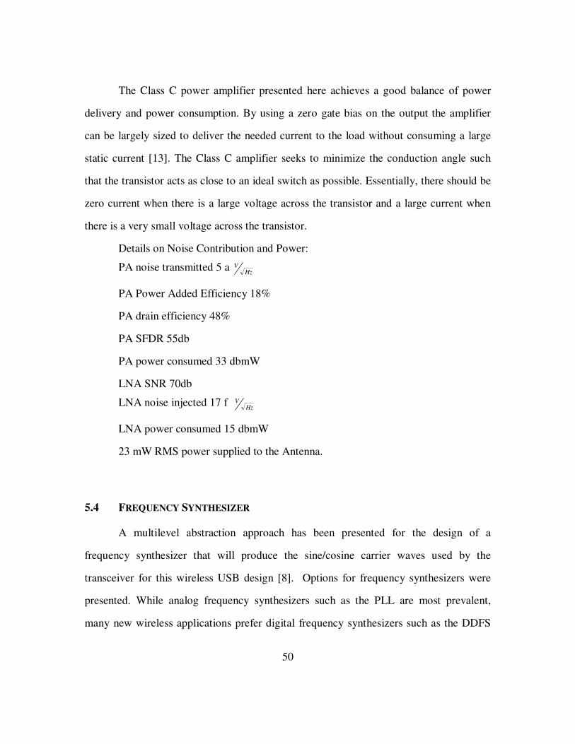
The Class C power amplifier presented here achieves a good balance of power
delivery and power consumption. By using a zero gate bias on the output the amplifier
can be largely sized to deliver the needed current to the load without consuming a large
static current [13]. The Class C amplifier seeks to minimize the conduction angle such
that the transistor acts as close to an ideal switch as possible. Essentially, there should be
zero current when there is a large voltage across the transistor and a large current when
there is a very small voltage across the transistor.
Details on Noise Contribution and Power:
PA noise transmitted 5 a HzV
PA Power Added Efficiency 18%
PA drain efficiency 48%
PA SFDR 55db
PA power consumed 33 dbmW
LNA SNR 70db
LNA noise injected 17 f HzV
LNA power consumed 15 dbmW
23 mW RMS power supplied to the Antenna.
5.4 FREQUENCY SYNTHESIZER
A multilevel abstraction approach has been presented for the design of a
frequency synthesizer that will produce the sine/cosine carrier waves used by the
transceiver for this wireless USB design [8]. Options for frequency synthesizers were
presented. While analog frequency synthesizers such as the PLL are most prevalent,
many new wireless applications prefer digital frequency synthesizers such as the DDFS

51
because they provide high frequency accuracy, temperature and time stability, as well as
being frequency agile and phase continuous. The best feature that is most often forgotten
is that digital frequency synthesizers do not need to be tuned, and hence could provide
lower test time and potentially lower costs.
Reference [8] also illustrates the system level consideration about which design of
digital frequency synthesizers to choose and analysis on optimal settings for the DDFS to
meet specifications for the design. The analysis shows that a 64 entry LUT, with 5 bits
output (excluding 1 bit for sign), can produce a SQNR of greater than 30dB and SFDR of
greater than 55dBc.
At a 100MHz operating frequency, at room temperature and using TSMC 0.18u
3.3V technology, each ROM for the folded ROM architecture produce an average power
of 3.5 mW, the 8-bit RCA adder produce an average power of 1.2 mW and the 2 8-bit
registers that store the phase offset produce an average power of 0.7 mW. Excluding the
power consumption of DAC, the total power consumption of the digital frequency
synthesizer is less than 10 mW [8].
5.5 SUMMARY
The transceiver presented can be used in two configurations: it can be attached to
a USB host that has its own power supply, or it can be attached to a device that is
powered by batteries. In the first case, the device must draw less than 200 mA of current
in order to be powered by the USB bus [5]. However, in the second case, when the
transceiver would be connected to battery powered devices such as digital cameras, it
would be nice if it could function continuously on a single AA lithium battery for an
entire day. In battery connected mode, the transceiver should only draw current during
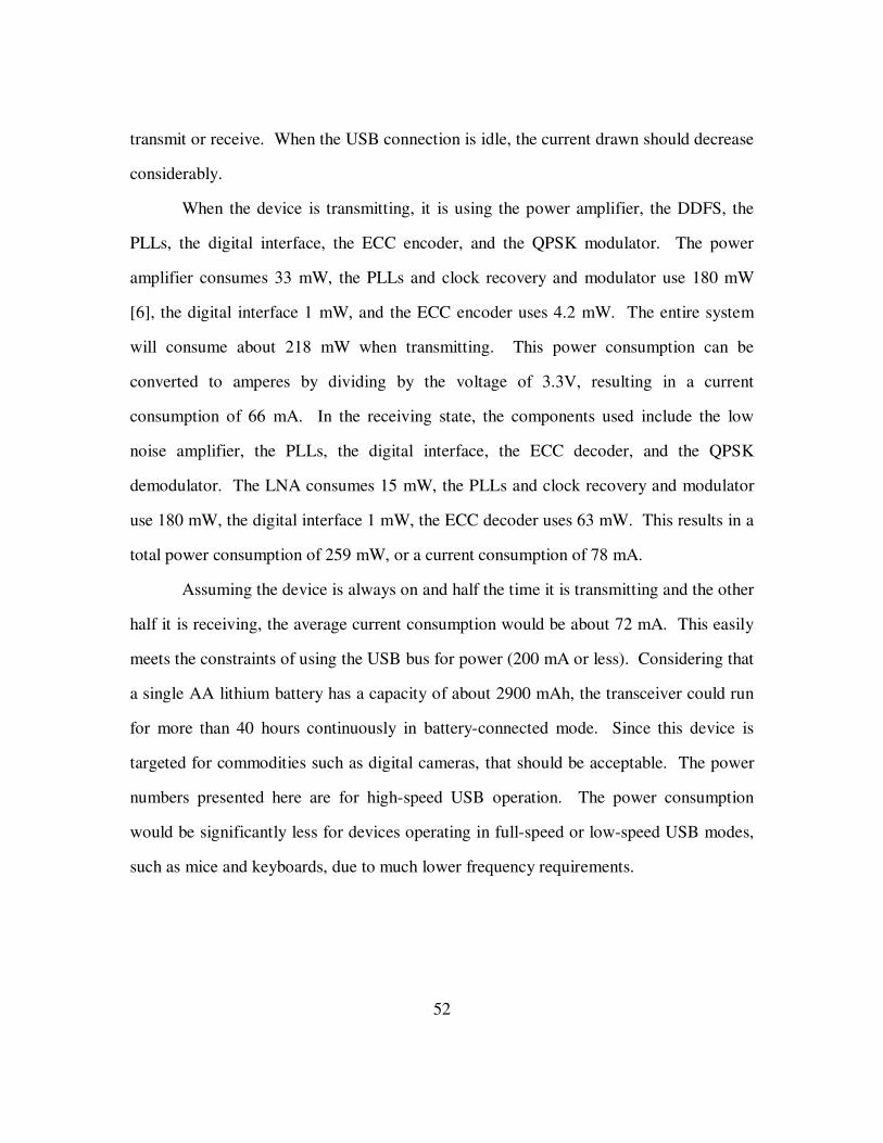
52
transmit or receive. When the USB connection is idle, the current drawn should decrease
considerably.
When the device is transmitting, it is using the power amplifier, the DDFS, the
PLLs, the digital interface, the ECC encoder, and the QPSK modulator. The power
amplifier consumes 33 mW, the PLLs and clock recovery and modulator use 180 mW
[6], the digital interface 1 mW, and the ECC encoder uses 4.2 mW. The entire system
will consume about 218 mW when transmitting. This power consumption can be
converted to amperes by dividing by the voltage of 3.3V, resulting in a current
consumption of 66 mA. In the receiving state, the components used include the low
noise amplifier, the PLLs, the digital interface, the ECC decoder, and the QPSK
demodulator. The LNA consumes 15 mW, the PLLs and clock recovery and modulator
use 180 mW, the digital interface 1 mW, the ECC decoder uses 63 mW. This results in a
total power consumption of 259 mW, or a current consumption of 78 mA.
Assuming the device is always on and half the time it is transmitting and the other
half it is receiving, the average current consumption would be about 72 mA. This easily
meets the constraints of using the USB bus for power (200 mA or less). Considering that
a single AA lithium battery has a capacity of about 2900 mAh, the transceiver could run
for more than 40 hours continuously in battery-connected mode. Since this device is
targeted for commodities such as digital cameras, that should be acceptable. The power
numbers presented here are for high-speed USB operation. The power consumption
would be significantly less for devices operating in full-speed or low-speed USB modes,
such as mice and keyboards, due to much lower frequency requirements.
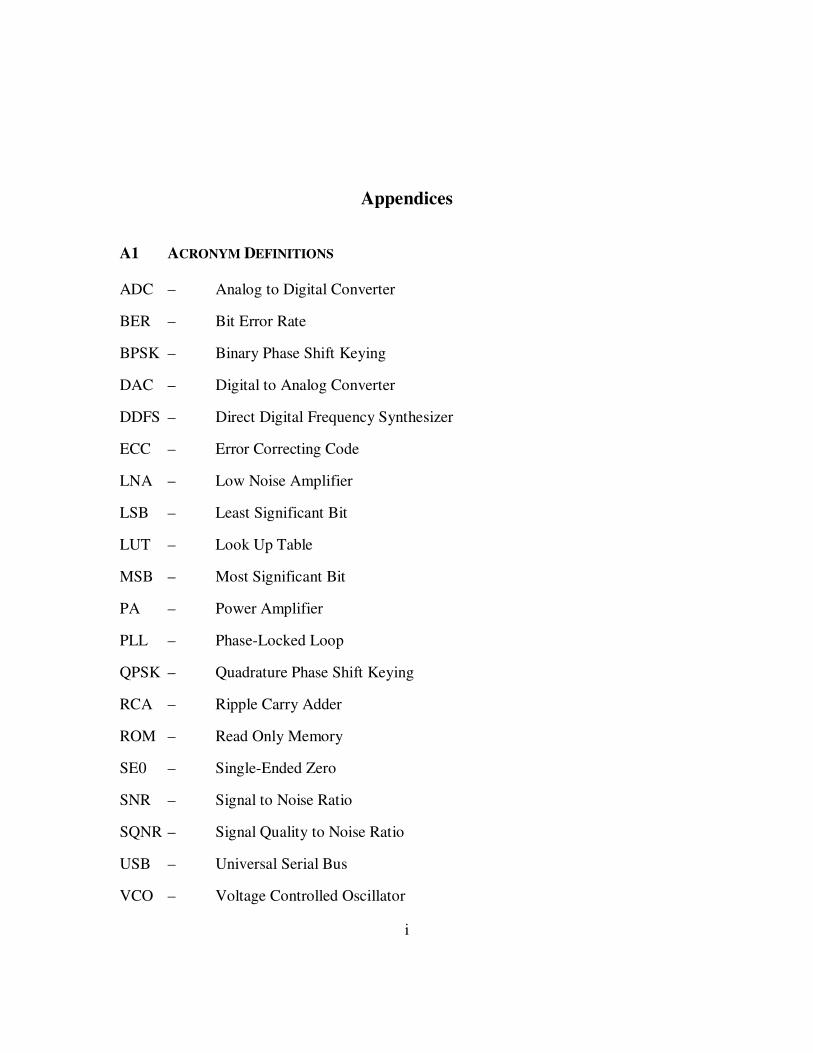
i
Appendices
A1 ACRONYM DEFINITIONS
ADC – Analog to Digital Converter
BER – Bit Error Rate
BPSK – Binary Phase Shift Keying
DAC – Digital to Analog Converter
DDFS – Direct Digital Frequency Synthesizer
ECC – Error Correcting Code
LNA – Low Noise Amplifier
LSB – Least Significant Bit
LUT – Look Up Table
MSB – Most Significant Bit
PA – Power Amplifier
PLL – Phase-Locked Loop
QPSK – Quadrature Phase Shift Keying
RCA – Ripple Carry Adder
ROM – Read Only Memory
SE0 – Single-Ended Zero
SNR – Signal to Noise Ratio
SQNR – Signal Quality to Noise Ratio
USB – Universal Serial Bus
VCO – Voltage Controlled Oscillator
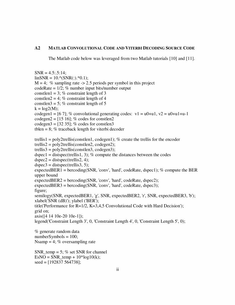
ii
A2 MATLAB CONVOLUTIONAL CODE AND VITERBI DECODING SOURCE CODE
The Matlab code below was leveraged from two Matlab tutorials [10] and [11].
SNR = 4.5:.5:14; linSNR = 10.^(SNR(:).*0.1); M = 4; % sampling rate -> 2.5 periods per symbol in this project codeRate = 1/2; % number input bits/number output constlen1 = 3; % constraint length of 3 constlen2 = 4; % constraint length of 4 constlen3 = 5; % constraint length of 5 k = log2(M); codegen1 = [6 7]; % convolutional generating codes: v1 = u0+u1, v2 = u0+u1+u-1 codegen2 = [15 16]; % codes for constlen2 codegen3 = [32 35]; % codes for constlen3 tblen = 8; % traceback length for viterbi decoder trellis1 = poly2trellis(constlen1, codegen1); % create the trellis for the encoder trellis2 = poly2trellis(constlen2, codegen2); trellis3 = poly2trellis(constlen3, codegen3); dspec1 = distspec(trellis1, 3); % compute the distances between the codes dspec2 = distspec(trellis2, 4); dspec3 = distspec(trellis3, 5); expectedBER1 = bercoding(SNR, 'conv', 'hard', codeRate, dspec1); % compute the BER upper bound expectedBER2 = bercoding(SNR, 'conv', 'hard', codeRate, dspec2); expectedBER3 = bercoding(SNR, 'conv', 'hard', codeRate, dspec3); figure; semilogy(SNR, expectedBER1, 'g', SNR, expectedBER2, 'r', SNR, expectedBER3, 'b'); xlabel('SNR (dB)'); ylabel ('BER'); title('Performance for R=1/2, K=3,4,5 Convolutional Code with Hard Decision'); grid on; axis([4 14 10e-20 10e-1]); legend('Constraint Length 3', 0, 'Constraint Length 4', 0, 'Constraint Length 5', 0); % generate random data numberSymbols = 100; Nsamp = 4; % oversampling rate SNR_temp = 5; % set SNR for channel EsNO = SNR_temp + 10*log10(k); seed = [192837 564738];
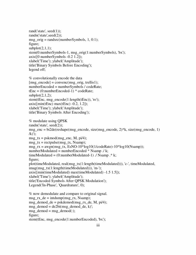
iii
rand('state', seed(1)); randn('state',seed(2)); msg_orig = randsrc(numberSymbols, 1, 0:1); figure; subplot(2,1,1); stem(0:numberSymbols-1, msg_orig(1:numberSymbols), 'bx'); axis([0 numberSymbols -0.2 1.2]); xlabel('Time'); ylabel('Amplitude'); title('Binary Symbols Before Encoding'); legend off; % convolutionally encode the data [msg_encode] = convenc(msg_orig, trellis1); numberEncoded = numberSymbols / codeRate; tEnc = (0:numberEncoded-1) * codeRate; subplot(2,1,2); stem(tEnc, msg_encode(1:length(tEnc)), 'ro'); axis([min(tEnc) max(tEnc) -0.2, 1.2]); xlabel('Time'); ylabel('Amplitude'); title('Binary Symbols After Encoding'); % modulate using QPSK randn('state', seed(2)); msg_enc = bi2de(reshape(msg_encode, size(msg_encode, 2)*k, size(msg_encode, 1) /k)'); msg_tx = pskmod(msg_enc, M, pi/4); msg_tx = rectpulse(msg_tx, Nsamp); msg_rx = awgn(msg_tx, EsNO-10*log10(1/codeRate)-10*log10(Nsamp)); numberModulated = numberEncoded * Nsamp ./ k; timeModulated = (0:numberModulated-1) ./ Nsamp .* k; figure; plot(timeModulated, real(msg_tx(1:length(timeModulated))), 'c-', timeModulated, imag(msg_tx(1:length(timeModulated))), 'm-'); axis([min(timeModulated) max(timeModulated) -1.5 1.5]); xlabel('Time'); ylabel('Amplitude'); title('Encoded Symbols After QPSK Modulation'); Legend('In-Phase', 'Quardrature', 0); % now demodulate and compare to original signal. msg_rx_de = intdump(msg_rx, Nsamp); msg_demod_de = pskdemod(msg_rx_de, M, pi/4); msg_demod = de2bi(msg_demod_de, k)'; msg_demod = msg_demod(:); figure; stem(tEnc, msg_encode(1:numberEncoded), 'bx');
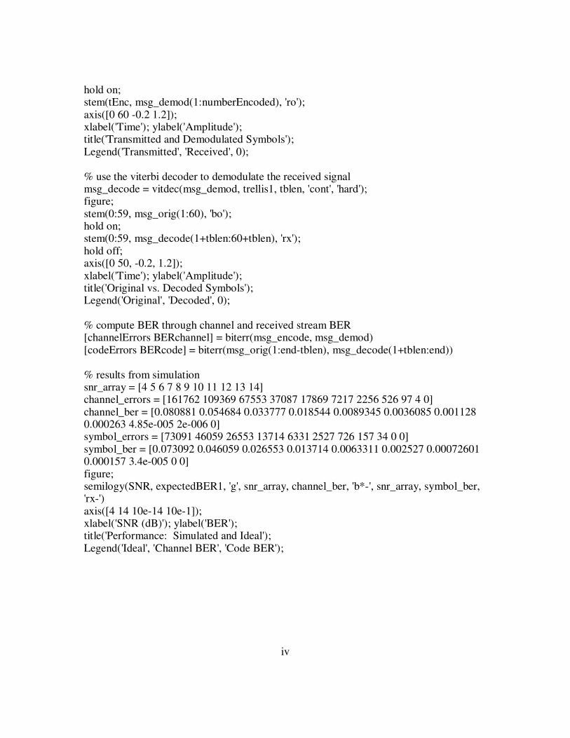
iv
hold on; stem(tEnc, msg_demod(1:numberEncoded), 'ro'); axis([0 60 -0.2 1.2]); xlabel('Time'); ylabel('Amplitude'); title('Transmitted and Demodulated Symbols'); Legend('Transmitted', 'Received', 0); % use the viterbi decoder to demodulate the received signal msg_decode = vitdec(msg_demod, trellis1, tblen, 'cont', 'hard'); figure; stem(0:59, msg_orig(1:60), 'bo'); hold on; stem(0:59, msg_decode(1+tblen:60+tblen), 'rx'); hold off; axis([0 50, -0.2, 1.2]); xlabel('Time'); ylabel('Amplitude'); title('Original vs. Decoded Symbols'); Legend('Original', 'Decoded', 0); % compute BER through channel and received stream BER [channelErrors BERchannel] = biterr(msg_encode, msg_demod) [codeErrors BERcode] = biterr(msg_orig(1:end-tblen), msg_decode(1+tblen:end)) % results from simulation snr_array = [4 5 6 7 8 9 10 11 12 13 14] channel_errors = [161762 109369 67553 37087 17869 7217 2256 526 97 4 0] channel_ber = [0.080881 0.054684 0.033777 0.018544 0.0089345 0.0036085 0.001128 0.000263 4.85e-005 2e-006 0] symbol_errors = [73091 46059 26553 13714 6331 2527 726 157 34 0 0] symbol_ber = [0.073092 0.046059 0.026553 0.013714 0.0063311 0.002527 0.00072601 0.000157 3.4e-005 0 0] figure; semilogy(SNR, expectedBER1, 'g', snr_array, channel_ber, 'b*-', snr_array, symbol_ber, 'rx-') axis([4 14 10e-14 10e-1]); xlabel('SNR (dB)'); ylabel('BER'); title('Performance: Simulated and Ideal'); Legend('Ideal', 'Channel BER', 'Code BER');
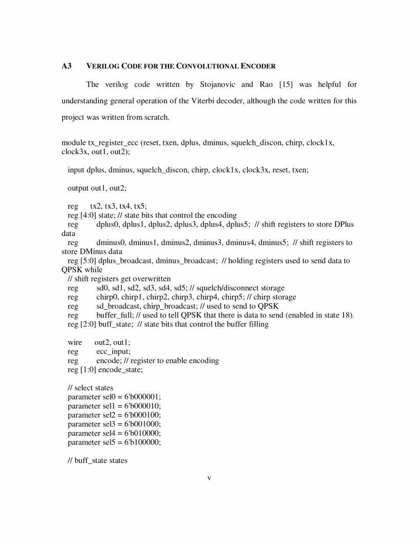
v
A3 VERILOG CODE FOR THE CONVOLUTIONAL ENCODER
The verilog code written by Stojanovic and Rao [15] was helpful for
understanding general operation of the Viterbi decoder, although the code written for this
project was written from scratch.
module tx_register_ecc (reset, txen, dplus, dminus, squelch_discon, chirp, clock1x, clock3x, out1, out2); input dplus, dminus, squelch_discon, chirp, clock1x, clock3x, reset, txen; output out1, out2; reg tx2, tx3, tx4, tx5; reg [4:0] state; // state bits that control the encoding reg dplus0, dplus1, dplus2, dplus3, dplus4, dplus5; // shift registers to store DPlus data reg dminus0, dminus1, dminus2, dminus3, dminus4, dminus5; // shift registers to store DMinus data reg [5:0] dplus_broadcast, dminus_broadcast; // holding registers used to send data to QPSK while // shift registers get overwritten reg sd0, sd1, sd2, sd3, sd4, sd5; // squelch/disconnect storage reg chirp0, chirp1, chirp2, chirp3, chirp4, chirp5; // chirp storage reg sd_broadcast, chirp_broadcast; // used to send to QPSK reg buffer_full; // used to tell QPSK that there is data to send (enabled in state 18). reg [2:0] buff_state; // state bits that control the buffer filling wire out2, out1; reg ecc_input; reg encode; // register to enable encoding reg [1:0] encode_state; // select states parameter sel0 = 6'b000001; parameter sel1 = 6'b000010; parameter sel2 = 6'b000100; parameter sel3 = 6'b001000; parameter sel4 = 6'b010000; parameter sel5 = 6'b100000; // buff_state states
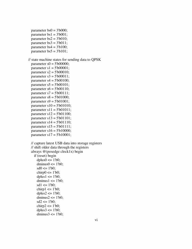
vi
parameter bs0 = 3'b000; parameter bs1 = 3'b001; parameter bs2 = 3'b010; parameter bs3 = 3'b011; parameter bs4 = 3'b100; parameter bs5 = 3'b101; // state machine states for sending data to QPSK parameter s0 = 5'b00000; parameter s1 = 5'b00001; parameter s2 = 5'b00010; parameter s3 = 5'b00011; parameter s4 = 5'b00100; parameter s5 = 5'b00101; parameter s6 = 5'b00110; parameter s7 = 5'b00111; parameter s8 = 5'b01000; parameter s9 = 5'b01001; parameter s10 = 5'b01010; parameter s11 = 5'b01011; parameter s12 = 5'b01100; parameter s13 = 5'b01101; parameter s14 = 5'b01110; parameter s15 = 5'b01111; parameter s16 = 5'b10000; parameter s17 = 5'b10001; // capture latest USB data into storage registers // shift older data through the registers always @(posedge clock1x) begin if (reset) begin dplus0 <= 1'b0; dminus0 <= 1'b0; sd0 <= 1'b0; chirp0 <= 1'b0; dplus1 <= 1'b0; dminus1 <= 1'b0; sd1 <= 1'b0; chirp1 <= 1'b0; dplus2 <= 1'b0; dminus2 <= 1'b0; sd2 <= 1'b0; chirp2 <= 1'b0; dplus3 <= 1'b0; dminus3 <= 1'b0;
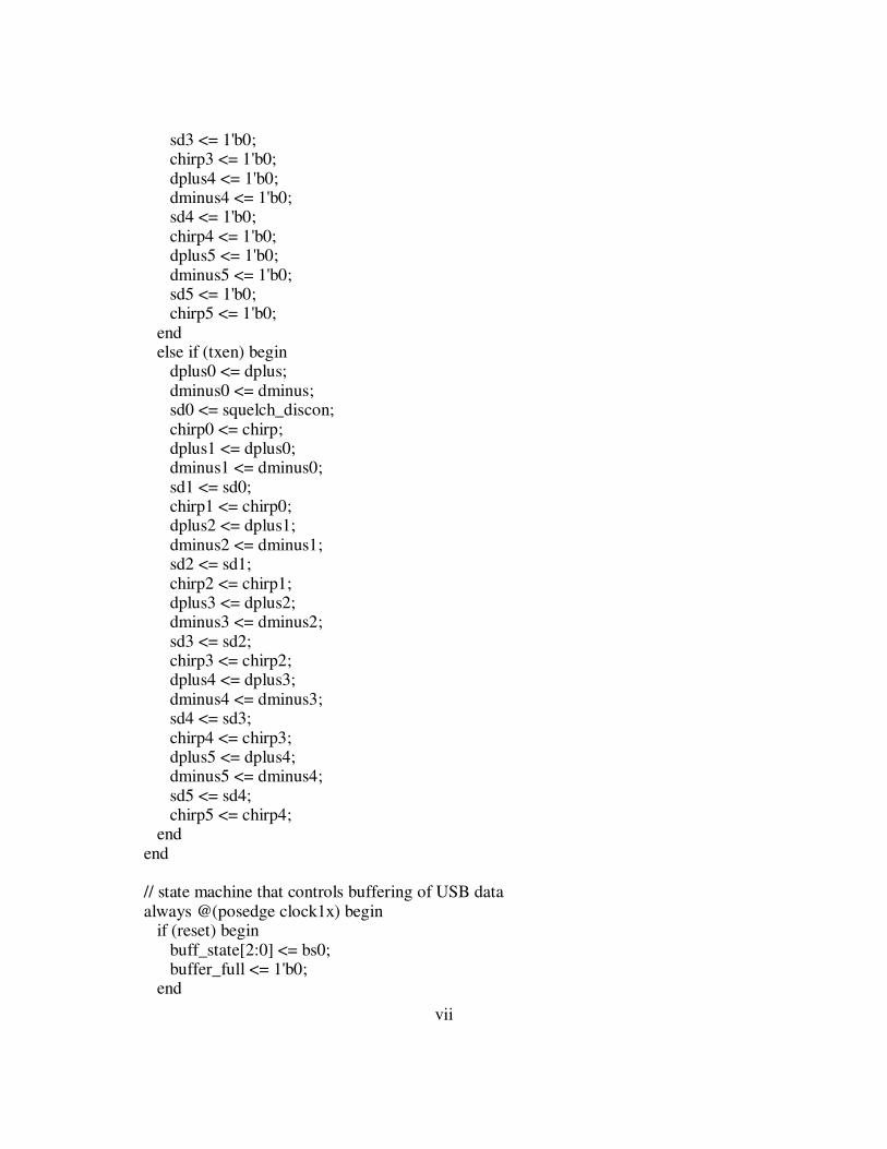
vii
sd3 <= 1'b0; chirp3 <= 1'b0; dplus4 <= 1'b0; dminus4 <= 1'b0; sd4 <= 1'b0; chirp4 <= 1'b0; dplus5 <= 1'b0; dminus5 <= 1'b0; sd5 <= 1'b0; chirp5 <= 1'b0; end else if (txen) begin dplus0 <= dplus; dminus0 <= dminus; sd0 <= squelch_discon; chirp0 <= chirp; dplus1 <= dplus0; dminus1 <= dminus0; sd1 <= sd0; chirp1 <= chirp0; dplus2 <= dplus1; dminus2 <= dminus1; sd2 <= sd1; chirp2 <= chirp1; dplus3 <= dplus2; dminus3 <= dminus2; sd3 <= sd2; chirp3 <= chirp2; dplus4 <= dplus3; dminus4 <= dminus3; sd4 <= sd3; chirp4 <= chirp3; dplus5 <= dplus4; dminus5 <= dminus4; sd5 <= sd4; chirp5 <= chirp4; end end // state machine that controls buffering of USB data always @(posedge clock1x) begin if (reset) begin buff_state[2:0] <= bs0; buffer_full <= 1'b0; end
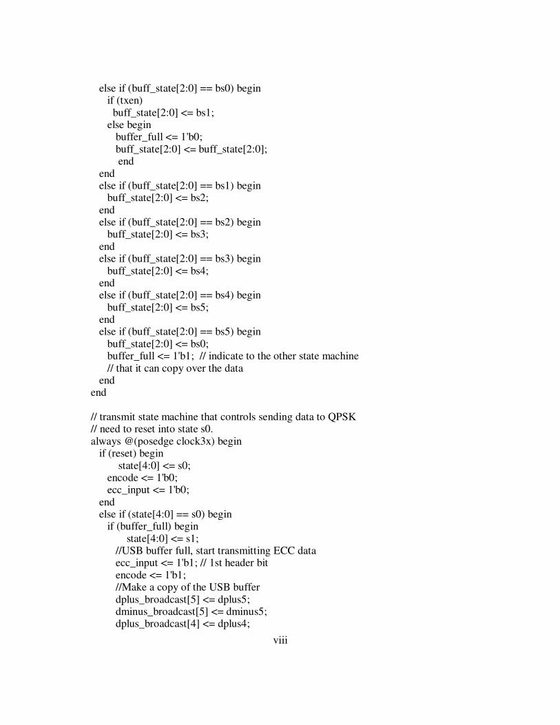
viii
else if (buff_state[2:0] == bs0) begin if (txen) buff_state[2:0] <= bs1; else begin buffer_full <= 1'b0; buff_state[2:0] <= buff_state[2:0]; end end else if (buff_state[2:0] == bs1) begin buff_state[2:0] <= bs2; end else if (buff_state[2:0] == bs2) begin buff_state[2:0] <= bs3; end else if (buff_state[2:0] == bs3) begin buff_state[2:0] <= bs4; end else if (buff_state[2:0] == bs4) begin buff_state[2:0] <= bs5; end else if (buff_state[2:0] == bs5) begin buff_state[2:0] <= bs0; buffer_full <= 1'b1; // indicate to the other state machine // that it can copy over the data end end // transmit state machine that controls sending data to QPSK // need to reset into state s0. always @(posedge clock3x) begin if (reset) begin state[4:0] <= s0; encode <= 1'b0; ecc_input <= 1'b0; end else if (state[4:0] == s0) begin if (buffer_full) begin state[4:0] <= s1; //USB buffer full, start transmitting ECC data ecc_input <= 1'b1; // 1st header bit encode <= 1'b1; //Make a copy of the USB buffer dplus_broadcast[5] <= dplus5; dminus_broadcast[5] <= dminus5; dplus_broadcast[4] <= dplus4;

ix
dminus_broadcast[4] <= dminus4; dplus_broadcast[3] <= dplus3; dminus_broadcast[3] <= dminus3; dplus_broadcast[2] <= dplus2; dminus_broadcast[2] <= dminus2; dplus_broadcast[1] <= dplus1; dminus_broadcast[1] <= dminus1; dplus_broadcast[0] <= dplus0; dminus_broadcast[0] <= dminus0; //minimize SD & Chirp data sd_broadcast <= sd5 | sd4 | sd3 | sd2 | sd1 | sd0; chirp_broadcast <= chirp5 | chirp4 | chirp3 | chirp2 | chirp1 | chirp0; end // if (buffer_full) else begin encode <= 1'b0; state[4:0] <= s0; end end // if (buffer_full) else if (state[4:0] == s1) begin state[4:0] <= s2; ecc_input <= 1'b1; // 2nd header bit end else if (state[4:0] == s2) begin state[4:0] <= s3; ecc_input <= dplus_broadcast[5]; //1st D+ bit end else if (state[4:0] == s3) begin state[4:0] <= s4; ecc_input <= dminus_broadcast[5]; //1st D- bit end else if (state[4:0] == s4) begin state[4:0] <= s5; ecc_input <= dplus_broadcast[4]; //2nd D+ bit end else if (state[4:0] == s5) begin state[4:0] <= s6; ecc_input <= dminus_broadcast[4]; //2nd D- bit end else if (state[4:0] == s6) begin state[4:0] <= s7; ecc_input <= dplus_broadcast[3]; // 3rd D+ bit end else if (state[4:0] == s7) begin
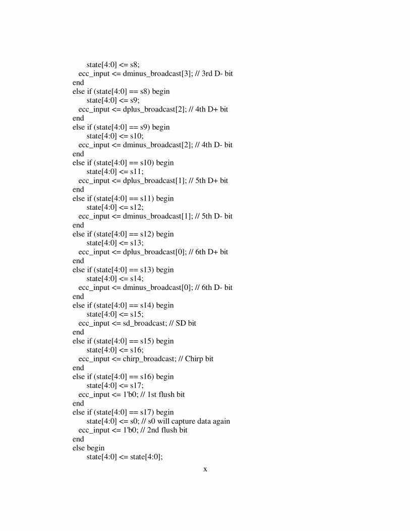
x
state[4:0] <= s8; ecc_input <= dminus_broadcast[3]; // 3rd D- bit end else if (state[4:0] == s8) begin state[4:0] <= s9; ecc_input <= dplus_broadcast[2]; // 4th D+ bit end else if (state[4:0] == s9) begin state[4:0] <= s10; ecc_input <= dminus_broadcast[2]; // 4th D- bit end else if (state[4:0] == s10) begin state[4:0] <= s11; ecc_input <= dplus_broadcast[1]; // 5th D+ bit end else if (state[4:0] == s11) begin state[4:0] <= s12; ecc_input <= dminus_broadcast[1]; // 5th D- bit end else if (state[4:0] == s12) begin state[4:0] <= s13; ecc_input <= dplus_broadcast[0]; // 6th D+ bit end else if (state[4:0] == s13) begin state[4:0] <= s14; ecc_input <= dminus_broadcast[0]; // 6th D- bit end else if (state[4:0] == s14) begin state[4:0] <= s15; ecc_input <= sd_broadcast; // SD bit end else if (state[4:0] == s15) begin state[4:0] <= s16; ecc_input <= chirp_broadcast; // Chirp bit end else if (state[4:0] == s16) begin state[4:0] <= s17; ecc_input <= 1'b0; // 1st flush bit end else if (state[4:0] == s17) begin state[4:0] <= s0; // s0 will capture data again ecc_input <= 1'b0; // 2nd flush bit end else begin state[4:0] <= state[4:0];
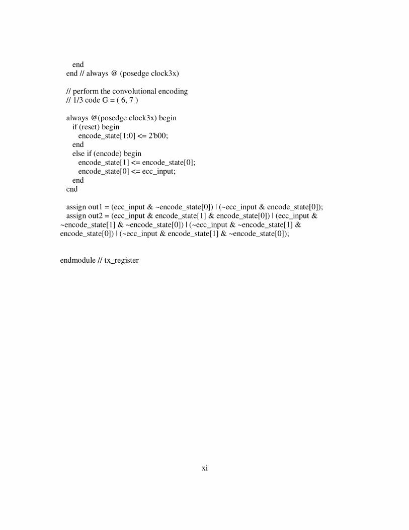
xi
end end // always @ (posedge clock3x) // perform the convolutional encoding // 1/3 code G = ( 6, 7 ) always @(posedge clock3x) begin if (reset) begin encode_state[1:0] <= 2'b00; end else if (encode) begin encode_state[1] <= encode_state[0]; encode_state[0] <= ecc_input; end end assign out1 = (ecc_input & ~encode_state[0]) | (~ecc_input & encode_state[0]); assign out2 = (ecc_input & encode_state[1] & encode_state[0]) | (ecc_input & ~encode_state[1] & ~encode_state[0]) | (~ecc_input & ~encode_state[1] & encode_state[0]) | (~ecc_input & encode_state[1] & ~encode_state[0]); endmodule // tx_register
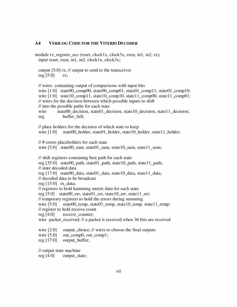
xii
A4 VERILOG CODE FOR THE VITERBI DECODER module rx_register_ecc (reset, clock1x, clock3x, rxen, in1, in2, rx); input reset, rxen, in1, in2, clock1x, clock3x; output [5:0] rx; // output to send to the transceiver reg [5:0] rx; // wires containing output of comparisons with input bits wire [1:0] state00_comp00, state00_comp01, state01_comp11, state01_comp10; wire [1:0] state10_comp11, state10_comp10, state11_comp00, state11_comp01; // wires for the decision between which possible inputs to shift // into the possible paths for each state wire state00_decision, state01_decision, state10_decision, state11_decision; reg buffer_full; // place holders for the decision of which state to keep wire [1:0] state00_holder, state01_holder, state10_holder, state11_holder; // # errors placeholders for each state wire [5:0] state00_sum, state01_sum, state10_sum, state11_sum; // shift registers containing best path for each state reg [35:0] state00_path, state01_path, state10_path, state11_path; // state decoded data reg [17:0] state00_data, state01_data, state10_data, state11_data; // decoded data to be broadcast reg [15:0] rx_data; // registers to hold hamming metric data for each state reg [5:0] state00_err, state01_err, state10_err, state11_err; // temporary registers to hold the errors during summing wire [5:0] state00_temp, state01_temp, state10_temp, state11_temp; // register to hold receive count reg [4:0] receive_counter; wire packet_received; // a packet is received when 36 bits are received wire [2:0] output_choice; // wires to choose the final outputs wire [5:0] out_comp0, out_comp1; reg [17:0] output_buffer; // output state machine reg [4:0] output_state;
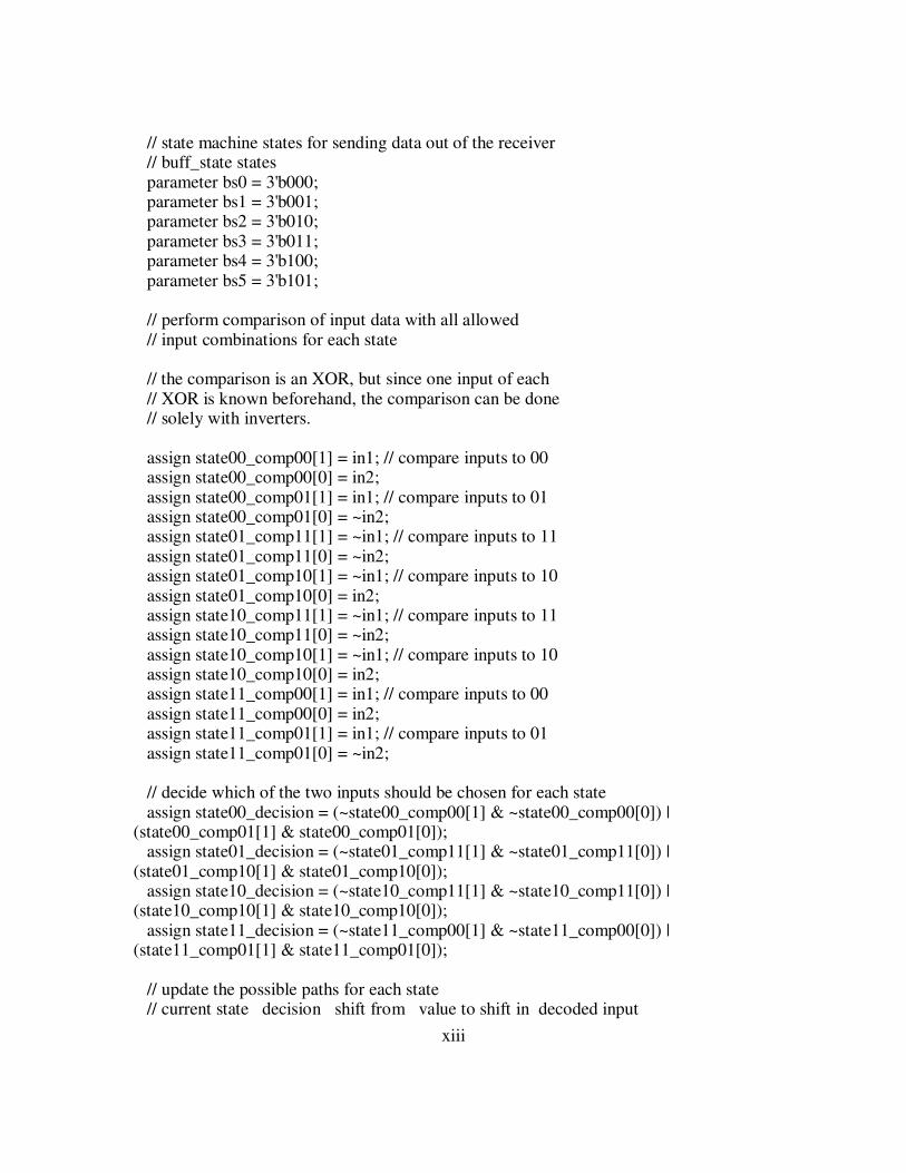
xiii
// state machine states for sending data out of the receiver // buff_state states parameter bs0 = 3'b000; parameter bs1 = 3'b001; parameter bs2 = 3'b010; parameter bs3 = 3'b011; parameter bs4 = 3'b100; parameter bs5 = 3'b101; // perform comparison of input data with all allowed // input combinations for each state // the comparison is an XOR, but since one input of each // XOR is known beforehand, the comparison can be done // solely with inverters. assign state00_comp00[1] = in1; // compare inputs to 00 assign state00_comp00[0] = in2; assign state00_comp01[1] = in1; // compare inputs to 01 assign state00_comp01[0] = ~in2; assign state01_comp11[1] = ~in1; // compare inputs to 11 assign state01_comp11[0] = ~in2; assign state01_comp10[1] = ~in1; // compare inputs to 10 assign state01_comp10[0] = in2; assign state10_comp11[1] = ~in1; // compare inputs to 11 assign state10_comp11[0] = ~in2; assign state10_comp10[1] = ~in1; // compare inputs to 10 assign state10_comp10[0] = in2; assign state11_comp00[1] = in1; // compare inputs to 00 assign state11_comp00[0] = in2; assign state11_comp01[1] = in1; // compare inputs to 01 assign state11_comp01[0] = ~in2; // decide which of the two inputs should be chosen for each state assign state00_decision = (~state00_comp00[1] & ~state00_comp00[0]) | (state00_comp01[1] & state00_comp01[0]); assign state01_decision = (~state01_comp11[1] & ~state01_comp11[0]) | (state01_comp10[1] & state01_comp10[0]); assign state10_decision = (~state10_comp11[1] & ~state10_comp11[0]) | (state10_comp10[1] & state10_comp10[0]); assign state11_decision = (~state11_comp00[1] & ~state11_comp00[0]) | (state11_comp01[1] & state11_comp01[0]); // update the possible paths for each state // current state decision shift from value to shift in decoded input
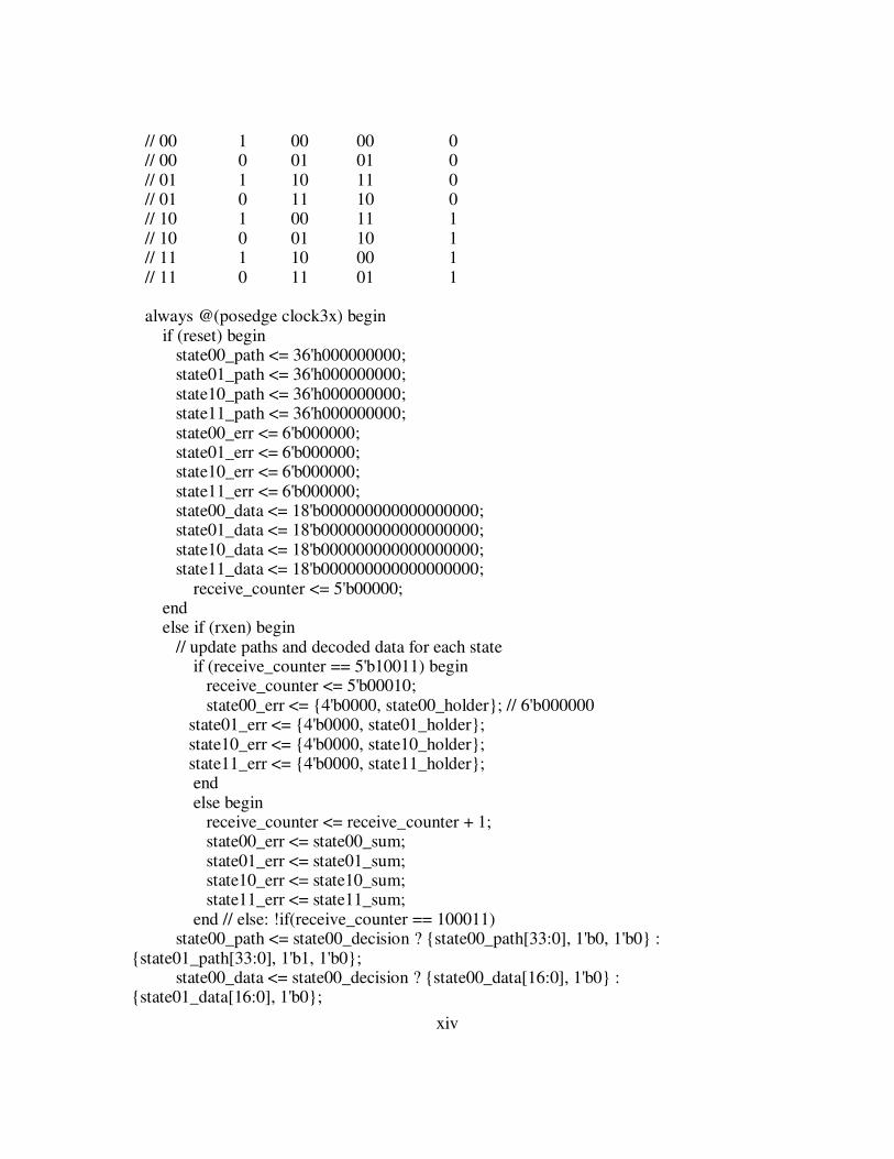
xiv
// 00 1 00 00 0 // 00 0 01 01 0 // 01 1 10 11 0 // 01 0 11 10 0 // 10 1 00 11 1 // 10 0 01 10 1 // 11 1 10 00 1 // 11 0 11 01 1 always @(posedge clock3x) begin if (reset) begin state00_path <= 36'h000000000; state01_path <= 36'h000000000; state10_path <= 36'h000000000; state11_path <= 36'h000000000; state00_err <= 6'b000000; state01_err <= 6'b000000; state10_err <= 6'b000000; state11_err <= 6'b000000; state00_data <= 18'b000000000000000000; state01_data <= 18'b000000000000000000; state10_data <= 18'b000000000000000000; state11_data <= 18'b000000000000000000; receive_counter <= 5'b00000; end else if (rxen) begin // update paths and decoded data for each state if (receive_counter == 5'b10011) begin receive_counter <= 5'b00010; state00_err <= {4'b0000, state00_holder}; // 6'b000000 state01_err <= {4'b0000, state01_holder}; state10_err <= {4'b0000, state10_holder}; state11_err <= {4'b0000, state11_holder}; end else begin receive_counter <= receive_counter + 1; state00_err <= state00_sum; state01_err <= state01_sum; state10_err <= state10_sum; state11_err <= state11_sum; end // else: !if(receive_counter == 100011) state00_path <= state00_decision ? {state00_path[33:0], 1'b0, 1'b0} : {state01_path[33:0], 1'b1, 1'b0}; state00_data <= state00_decision ? {state00_data[16:0], 1'b0} : {state01_data[16:0], 1'b0};
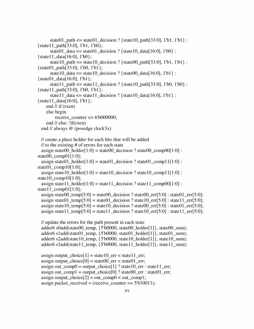
xv
state01_path <= state01_decision ? {state10_path[33:0], 1'b1, 1'b1} : {state11_path[33:0], 1'b1, 1'b0}; state01_data <= state01_decision ? {state10_data[16:0], 1'b0} : {state11_data[16:0], 1'b0}; state10_path <= state10_decision ? {state00_path[33:0], 1'b1, 1'b1} : {state01_path[33:0], 1'b0, 1'b1}; state10_data <= state10_decision ? {state00_data[16:0], 1'b1} : {state01_data[16:0], 1'b1}; state11_path <= state11_decision ? {state10_path[33:0], 1'b0, 1'b0} : {state11_path[33:0], 1'b0, 1'b1}; state11_data <= state11_decision ? {state10_data[16:0], 1'b1} : {state11_data[16:0], 1'b1}; end // if (rxen) else begin receive_counter <= 6'b000000; end // else: !if(rxen) end // always @ (posedge clock3x) // create a place holder for each bits that will be added // to the existing # of errors for each state assign state00_holder[1:0] = state00_decision ? state00_comp00[1:0] : state00_comp01[1:0]; assign state01_holder[1:0] = state01_decision ? state01_comp11[1:0] : state01_comp10[1:0]; assign state10_holder[1:0] = state10_decision ? state10_comp11[1:0] : state10_comp10[1:0]; assign state11_holder[1:0] = state11_decision ? state11_comp00[1:0] : state11_comp01[1:0]; assign state00_temp[5:0] = state00_decision ? state00_err[5:0] : state01_err[5:0]; assign state01_temp[5:0] = state01_decision ? state10_err[5:0] : state11_err[5:0]; assign state10_temp[5:0] = state10_decision ? state00_err[5:0] : state01_err[5:0]; assign state11_temp[5:0] = state11_decision ? state10_err[5:0] : state11_err[5:0]; // update the errors for the path present in each state adder6 s0add(state00_temp, {5'b0000, state00_holder[1]}, state00_sum); adder6 s1add(state01_temp, {5'b0000, state01_holder[1]}, state01_sum); adder6 s2add(state10_temp, {5'b0000, state10_holder[1]}, state10_sum); adder6 s3add(state11_temp, {5'b0000, state11_holder[1]}, state11_sum); assign output_choice[1] = state10_err < state11_err; assign output_choice[0] = state00_err < state01_err; assign out_comp0 = output_choice[1] ? state10_err : state11_err; assign out_comp1 = output_choice[0] ? state00_err : state01_err; assign output_choice[2] = out_comp0 < out_comp1; assign packet_received = (receive_counter == 5'b10011);
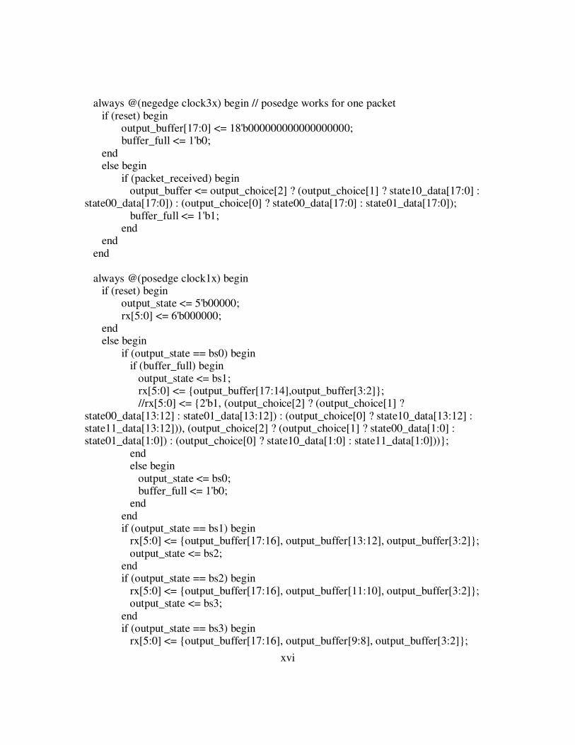
xvi
always @(negedge clock3x) begin // posedge works for one packet if (reset) begin output_buffer[17:0] <= 18'b000000000000000000; buffer_full <= 1'b0; end else begin if (packet_received) begin output_buffer <= output_choice[2] ? (output_choice[1] ? state10_data[17:0] : state00_data[17:0]) : (output_choice[0] ? state00_data[17:0] : state01_data[17:0]); buffer_full <= 1'b1; end end end always @(posedge clock1x) begin if (reset) begin output_state <= 5'b00000; rx[5:0] <= 6'b000000; end else begin if (output_state == bs0) begin if (buffer_full) begin output_state <= bs1; rx[5:0] <= {output_buffer[17:14],output_buffer[3:2]}; //rx[5:0] <= {2'b1, (output_choice[2] ? (output_choice[1] ? state00_data[13:12] : state01_data[13:12]) : (output_choice[0] ? state10_data[13:12] : state11_data[13:12])), (output_choice[2] ? (output_choice[1] ? state00_data[1:0] : state01_data[1:0]) : (output_choice[0] ? state10_data[1:0] : state11_data[1:0]))}; end else begin output_state <= bs0; buffer_full <= 1'b0; end end if (output_state == bs1) begin rx[5:0] <= {output_buffer[17:16], output_buffer[13:12], output_buffer[3:2]}; output_state <= bs2; end if (output_state == bs2) begin rx[5:0] <= {output_buffer[17:16], output_buffer[11:10], output_buffer[3:2]}; output_state <= bs3; end if (output_state == bs3) begin rx[5:0] <= {output_buffer[17:16], output_buffer[9:8], output_buffer[3:2]};

xvii
output_state <= bs4; end if (output_state == bs4) begin rx[5:0] <= {output_buffer[17:16], output_buffer[7:6], output_buffer[3:2]}; output_state <= bs5; end if (output_state == bs5) begin rx[5:0] <= {output_buffer[17:16], output_buffer[5:4], output_buffer[3:2]}; output_state <= bs0; end end end endmodule // rx_register_ecc module full_adder (a, b, cin, out, cout); input a, b, cin; output cout, out; assign out = (a & b & cin) | (a & ~b & ~cin) | (~a & b & ~cin) | (~a & ~b & cin); assign cout = (a & b) | (a & cin) | (b & cin); endmodule // full_adder module adder6 (a, b, sum); input [5:0] a, b; output [5:0] sum; wire [5:0] carry, sum; full_adder fa0(a[0], b[0], 1'b0, sum[0], carry[0]); full_adder fa1(a[1], b[1], carry[0], sum[1], carry[1]); full_adder fa2(a[2], b[2], carry[1], sum[2], carry[2]); full_adder fa3(a[3], b[3], carry[2], sum[3], carry[3]); full_adder fa4(a[4], b[4], carry[3], sum[4], carry[4]); full_adder fa5(a[5], b[5], carry[4], sum[5], carry[5]); endmodule // adder6
xviii
Works Cited
[1] Asghar, Saf, PhD. Personal Communication. Feb. 2005.
[2] Aziz, Adnan, PhD. Personal Communication. Summer 2005.
[3] Baldwin, Richard. “Information Theory and Creationism: Classical Information Theory (Shannon).” 2003. <http://home.mira.net/~reynella/debate/shannon.htm>.
[4] Clark, George C., Jr., and J. Bibb Cain. “Convolutional Code Structure and Viterbi Decoding.” Error-Correction Coding for Digital Communications. New York: Plenum Press, 1982. 227-66.
[5] Compaq, Et al. Universal Serial Bus Specification. Revision 2.0 ed. 2000.
[6] Dankert, Dan. “Wireless USB Transmit and Receive Scheme Clock Recovery Circuit”. Fall 2005.
[7] Fleming, Chip. A Tutorial on Convolutional Coding with Viterbi Decoding. 31 Jan. 2003. Sept. 2005 <http://home.netcom.com/~chip.f/viterbi/tutorial.html>.
[8] Gokhale, Sanjeev. “Design of a Digital Frequency Synthesizer for Wireless USB.” Fall 2005.
[9] Langton, Charan. “Tutorial 12 – Coding and Decoding with Convolutional Codes.” Complex2Real.com Complex Communications Technology Made Easy. July 1999. Sept. 2005 <http://www.complextoreal.com/chapters/convo.pdf>.
[10] Mathworks, The. “Covolutional Encoder and Viterbi Decoder - Demo”. Matlab Version 7. Apr. 2004.
[11] Mathworks, The. “Phase Shift Keying Simulation.” Matlab Version 7. Apr. 2004.
[12] McDermott, Mark. Personal Communication. Spring 2005.
[13] Patent, Dimitry. “Wireless USB RF Transceiver Circuitry.” Fall 2005.
[14] Poli, Alain, and Llorenc Huguet. “Application of Codes.” Error Correcting Codes Theory and Applications. Trans. Iain Craig. Hertfordshire, UK: Prentice Hall International Ltd, 1992. 410-58.
[15] Stojanovic, Vladimir, and Ketaki Rao. Viterbi Decoder - Verilog Code. July 2000. Sept. 2005 <http://mos.stanford.edu/ee272/proj99/babyviterbi/verilogcode.html>.

xix
Vita
Jacob S. Schneider was born February 13, 1979 in St. Louis, Missouri. He is the
son of Paul and Kathy Schneider. He received a Bachelors of Science in Electrical
Engineering from Rice University in Houston, Texas. He has worked at Intel
Corporation in Austin, Texas for the past four years as a circuit designer.
Permanent address: 3103 Stanwood Drive, Austin, Texas, 78757
This dissertation was typed by Jacob S. Schneider.