Copper interconnects - Gary Tuttle's ISU web...
16
copper – EE 432/532 1 Copper interconnects Copper advantages: 1. slightly better conductivity 2. much less susceptibility to electromigration Copper disadvantages: 1. Creates deep level defects in silicon (i.e. poisonous for electronic devices) 2. Difficult (even impossible) to etch by plasma methods Any method to utilize the advantages of copper must: 1. Keep the copper away from the silicon. Cannot be used for ohmic contacts, only for interconnects. 2. Patterns must be formed in a way that doesn’t require directly etching the copper.
-
Upload
dinhnguyet -
Category
Documents
-
view
219 -
download
3
Transcript of Copper interconnects - Gary Tuttle's ISU web...

copper –EE 432/532 1
Copper interconnects
Copper advantages:
1. slightly better conductivity
2. much less susceptibility to electromigration
Copper disadvantages:
1. Creates deep level defects in silicon (i.e. poisonous for electronic devices)
2. Difficult (even impossible) to etch by plasma methods
Any method to utilize the advantages of copper must:
1. Keep the copper away from the silicon. Cannot be used for ohmic contacts, only for interconnects.
2. Patterns must be formed in a way that doesn’t require directly etching the copper.

copper –EE 432/532 2

copper –EE 432/532 3
In middle ages, metal-smiths in Damascus developed processes for making intricately patterned, highly polished steel that was used extensively for making swords and knives. The steel was significantly better than anything else at the time. (Cutting edge technology!)
Damascene process
Technique for Damascus steel has been lost. Modern analysis of the metal shows that carbon nanotubes (!) are present and may have played a role in determining the properties.

copper –EE 432/532 4
1. Using plasma-enhanced CVD, grow a stacked structure of silicon dioxide and silicon nitride. The silicon nitride will serve as an etch-stop layer.
Damascene process
copper –EE 432/532 5
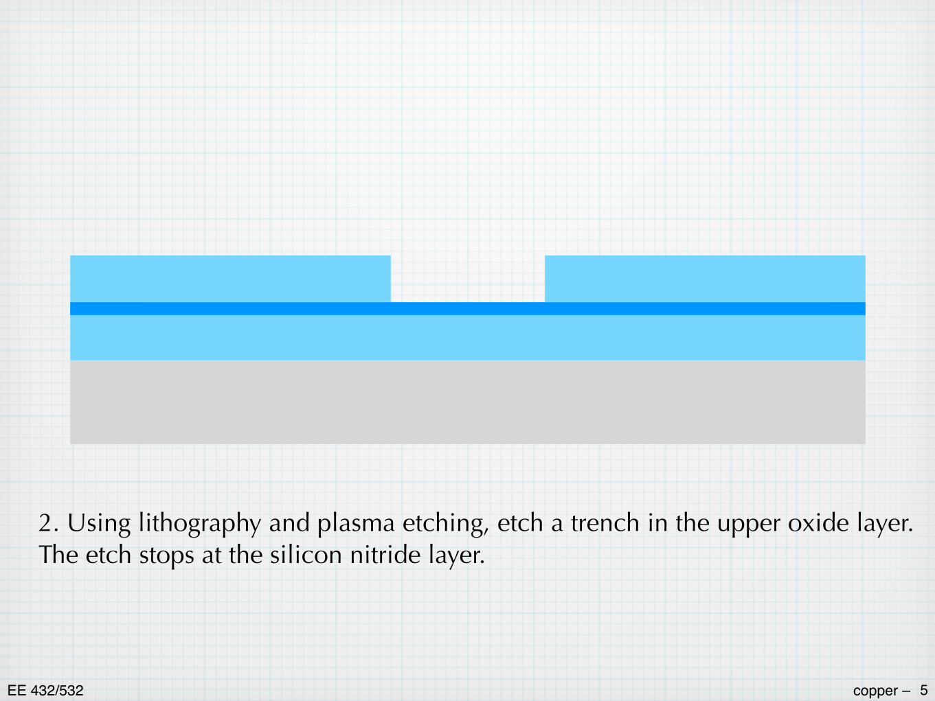
2. Using lithography and plasma etching, etch a trench in the upper oxide layer. The etch stops at the silicon nitride layer.
copper –EE 432/532 6
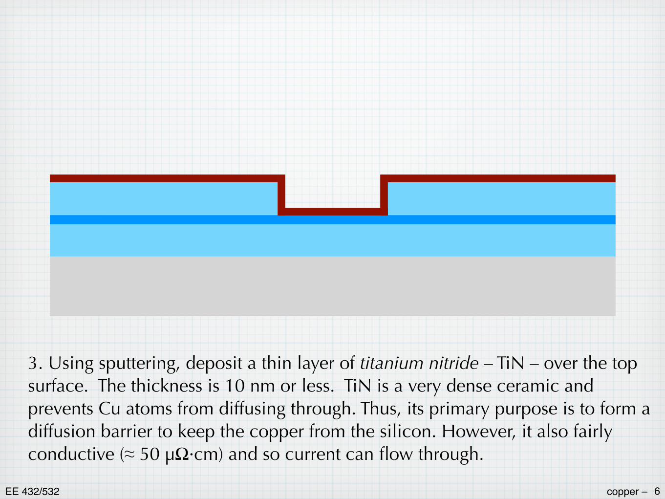
3. Using sputtering, deposit a thin layer of titanium nitride – TiN – over the top surface. The thickness is 10 nm or less. TiN is a very dense ceramic and prevents Cu atoms from diffusing through. Thus, its primary purpose is to form a diffusion barrier to keep the copper from the silicon. However, it also fairly conductive (≈ 50 µΩ·cm) and so current can flow through.

copper –EE 432/532 7
4. A thin layer of copper (≈ 10 nm) is sputtered over the TiN. The thin copper serves as a seed layer for the next step...

copper –EE 432/532 8
5. A thick layer of copper is deposited by electrolysis, using the seed layer as a starting point. This is essentially the same process that you may have used in grade school science class to deposit copper onto a spoon.

copper –EE 432/532 9
6. Finally chemical-mechanical planarization is used to grind away the upper portion of the copper, leaving only the portion in the trench. The top surface is flattened and ready for the next metalization step.

copper –EE 432/532 10
1. Using plasma-enhanced CVD, grow a stacked structure of silicon dioxide and silicon nitride.
Dual damascene processInter-level vias can also be incorporated with a slight modification.

copper –EE 432/532 11
2. Using lithography and plasma etching, etch a trench in the upper oxide layer. The etch stops at the silicon nitride layer.

copper –EE 432/532 12
3. Using lithography and plasma etching a second time, etch a via in the lower oxide layer. The etch stops at the underlying copper interconnect.

copper –EE 432/532 13
4. Using sputtering, deposit the thin TiN diffusion barrier.

copper –EE 432/532 14
5. Sputter on the thin seed layer of copper.

copper –EE 432/532 15
6. Deposit a thick layer of copper using electrolysis.

copper –EE 432/532 16
7. Use CMP to remove the excess copper, leaving behind the upper level interconnect and the via between the upper and lower connects.
With the dual damascene process, a separate via technology is not necessary. It is apparent why the TiN barrier material must also be conductive.