COP-GPC184-UK-5 - grifo
82
Via dell' Artigiano, 8/6 40016 San Giorgio di Piano (Bologna) ITALY E-mail: [email protected] http://www.grifo.it http://www.grifo.com Tel. +39 051 892.052 (a. r.) FAX: +39 051 893.661 , GPC ® , grifo ® , are trade marks of grifo ® grifo ® ITALIAN TECHNOLOGY TECHNICAL MANUAL GPC ® 184 General Purpose Controller Z180 GPC ® 184 Edition 5.10 Rel. 29 September 1999
Transcript of COP-GPC184-UK-5 - grifo

Via dell' Artigiano, 8/640016 San Giorgio di Piano(Bologna) ITALYE-mail: [email protected]
http://www.grifo.it http://www.grifo.comTel. +39 051 892.052 (a. r.) FAX: +39 051 893.661
, GPC®, grifo ®, are trade marks of grifo ®
grifo ®
ITALIAN TECHNOLOGY
TECHNICAL MANUAL
GPC® 184General Purpose Controller Z180
GPC® 184 Edition 5.10 Rel. 29 September 1999
Intelligent Module Abaco® BLOCK , Serie 4, size 100x50 mm; Optionalcontainer, format DIN 46277-1 and 3 rails compliant; CPU Z180, with18,432 MHz quartz; Configuration Jumper used to select RUN/DEBUGmode; Up to 512K of EPROM or FLASH and up to 512K of RAM ; RealTime Clock capable to generate INT errupts; Back Up circuitry for RAMand RTC, through on-board LITHIUM battery or external battery; ClockedSerial I/O interface, available to the User, on the I/O connetor; 2 internal16 bits wide Programmable Reload Timer channels; 2 RS232 serial lines,one of which settable as RS422, RS485 or Current Loop ; double BaudRate generator, software programmable; Watch Dog circuitery, hardwaremanageable; Abaco® I/O BUS da 26 pins expansion connector; 4 differentpower saving modes: Halt ,STOP, Sleep and System Stop; Power Failurecircuitry capable to generate interrupts; Consumption extermy reduced:only as low as 60 mA on 5Vdc; on-board logic protected against transientsby TransZorb™; Wide range of development software available such asRemote Symbolic Debugger; Macro Assembler; GET 80; C compilers(HI TECH C 80, DDS MICRO C 85); PASCAL compilers (PASCAL80, EMBEDDED PASCAL ); FGDOS184; etc.

DOCUMENTATION COPYRIGHT BY grifo ® , ALL RIGHTS RESERVED
No part of this document may be reproduced, transmitted, transcribed, stored in aretrieval system, or translated into any language or computer language, in any form orby any means, either electronic, mechanical, magnetic, optical, chemical, manual, orotherwise, without the prior written consent of grifo ®.
IMPORTANT
Although all the information contained herein have been carefully verified, grifo ®
assumes no responsability for errors that might appear in this document, or for damageto things or persons resulting from technical errors, omission and improper use of thismanual and of the related software and hardware.grifo ® reserves the right to change the contents and form of this document, as well as thefeatures and specification of its products at any time, without prior notice, to obtainalways the best product.For specific informations on the components mounted on the card, please refer to theData Book of the builder or second sources.
SYMBOLS DESCRIPTION
In the manual could appear the following symbols:
Attention: Generic danger
Attention: High voltage
Trade Marks
, GPC®, grifo ® : are trade marks of grifo ®.Other Product and Company names listed, are trade marks of their respective companies.

ITALIAN TECHNOLOGY grifo ®
Page I GPC® 184 Rel. 5.10
GENERAL INDEXINTRODUCTION ........................................................................................................................ 1
CARD VERSION.......................................................................................................................... 1
GENERAL FEATURES .............................................................................................................. 2 CPU ............................................................................................................................................. 3 MEMORY DEVICES ............................................................................................................... 3 SERIAL COMMUNICATION ................................................................................................. 4 CLOCK ...................................................................................................................................... 4 POWER SUPPLY ...................................................................................................................... 4 BOARD CONFIGURATION ................................................................................................... 4 ABACO® I/O BUS ...................................................................................................................... 6 REAL TIME CLOCK ............................................................................................................... 6 WATCH DOG ............................................................................................................................ 6 RESET CONTACT.................................................................................................................... 6 CONTROL LOGIC ................................................................................................................... 6
TECHNICAL FEATURES .......................................................................................................... 7 GENERAL FEATURES ........................................................................................................... 7 PHYSICAL FEATURES...........................................................................................................7 ELECTRIC FEATURES .......................................................................................................... 8
INSTALLATION .......................................................................................................................... 9 CONNECTIONS ....................................................................................................................... 9 CN2 - BACK UP EXTERNAL BATTERY CONNECTOR ................................................ 9 CN1 - ABACO® I/O BUS CONNECTOR ........................................................................... 10 CN3A - SERIAL LINE A CONNECTOR .......................................................................... 12 CN3B - SERIAL LINE B CONNECTOR .......................................................................... 14 CN5 - AUXILIARY SIGNALS CONNECTOR ................................................................. 20 I/O CONNECTION ................................................................................................................. 21 VISUAL SIGNALATIONS ..................................................................................................... 21 JUMPERS ................................................................................................................................ 22 2 PINS JUMPERS ................................................................................................................ 24 3 PINS JUMPERS ................................................................................................................ 25 5 PINS JUMPERS ................................................................................................................ 25 BACK UP ................................................................................................................................. 26 MEMORY SELECTION ........................................................................................................ 26 INTERRUPTS.......................................................................................................................... 27 CONFIGURATION INPUTS ................................................................................................. 27 SOLDER JUMPERS ............................................................................................................... 27 SERIAL COMMUNICATION SELECTION ...................................................................... 28 RESET AND WATCH DOG ................................................................................................... 30 POWER FAILURE.................................................................................................................. 31
SOFTWARE ................................................................................................................................ 32
grifo ® ITALIAN TECHNOLOGY
Page II GPC® 184 Rel. 5.10
DEVICES MAP AND ADDRESSES ........................................................................................ 35 INTRODUCTION ................................................................................................................... 35 ON BOARD DEVICES ADDRESSES ................................................................................... 35 ABACO® I/O BUS ADDRESSES............................................................................................ 35 MEMORY ADDRESSES ........................................................................................................ 36 I/O ADDRESSES ..................................................................................................................... 37
PERIPHERAL DEVICES SOFTWARE DESCRIPTION ..................................................... 39 REAL TIME CLOCK .............................................................................................................39 WATCH DOG .......................................................................................................................... 41 CONFIGURATION JUMPER ............................................................................................... 41 CPU INTERNAL PERIPHERALS ....................................................................................... 41
EXTERNAL CARDS .................................................................................................................42
BIBLIOGRAPHY....................................................................................................................... 44
APPENDIX A: CARD MECHANICAL MOUNTING ......................................................... A-1
APPENDIX B: ON BOARD DEVICES DESCRIPTION..................................................... B-1
APPENDIX C: ELECTRIC DIAGRAMS ............................................................................. C-1
APPENDICE D: ALPHABETICAL INDEX ......................................................................... D-1

ITALIAN TECHNOLOGY grifo ®
Page III GPC® 184 Rel. 5.10
FIGURES INDEXFIGURE 1: BLOCK DIAGRAM ............................................................................................................. 5FIGURE 2: CN2 - EXTERNAL BACK UP BATTERY CONNECTOR ............................................................. 9FIGURE 3 CN1 - ABACO® I/O BUS CONNECTOR ......................................................................... 10FIGURE 4: CARD PHOTO ................................................................................................................. 11FIGURE 5:COMPONENTS MAPS (SOLDERING SIDE AND COMPONENTS SIDE) ....................................... 11FIGURE 6: CN3A- SERIAL LINE A CONNECTOR .............................................................................. 12FIGURE 7: SERIAL COMMUNICATION DIAGRAM ................................................................................. 13FIGURE 8: CN3B- SERIAL LINE B CONNECTOR .............................................................................. 14FIGURE 9: LEDS, CONNECTORS, MEMORIES , ETC. LOCATION ........................................................... 15FIGURE 10: RS 232 PIN OUT AND CONNECTION EXAMPLE .............................................................. 16FIGURE 11: RS 422 PIN OUT AND POINT TO POINT CONNECTION EXAMPLE ...................................... 16FIGURE 12: RS 485 PIN OUT AND POINT TO POINT CONNECTION EXAMPLE ...................................... 16FIGURE 13: RS 485 PIN OUT AND NETWORK CONNECTION EXAMPLE .............................................. 17FIGURE 14: 4 WIRES CURRENT LOOP POINT TO POINT CONNECTION EXAMPLE .................................. 18FIGURE 15: 2 WIRES CURRENT LOOP POINT TO POINT CONNECTION EXAMPLE .................................. 18FIGURE 16: CN5 SIGNALS CONNECTION DIAGRAM .......................................................................... 19FIGURE 17: CN5 - AUXILIARY SIGNALS CONNECTOR ....................................................................... 20FIGURE 18: VISUAL SIGNALATIONS TABLE ........................................................................................ 21FIGURE 19: JUMPERS SUMMARIZING TABLE ..................................................................................... 22FIGURE 20: JUMPERS LOCATION (COMPONENT SIDE) ........................................................................ 23FIGURE 21: JUMPERS LOCATION (SOLDERING SIDE) ......................................................................... 23FIGURE 22: 2 PINS JUMPERS TABLE ................................................................................................. 24FIGURE 23: 3 PINS JUMPERS TABLE ................................................................................................. 25FIGURE 24: 5 PINS JUMPERS TABLE ................................................................................................. 25FIGURE 25: MEMORY SELECTION TABLE ......................................................................................... 26FIGURE 26: SERIAL COMMUNICATION DRIVER LOCATION .................................................................. 29FIGURE 27: MEMORY ALLOCATION ................................................................................................. 37FIGURE 28: I/O ADDRESSES TABLE .................................................................................................. 38FIGURE 29: AVAILABLE CONNECTIONS DIAGRAM .............................................................................. 43FIGURE A1: MODULE DIMENSION FOR PIGGY BACK MOUNTING ...................................................... A-1FIGURE A2: PIGGY BACK MOUNTING ............................................................................................ A-2FIGURE A3: WEIDMULLER RAIL MOUNTING .................................................................................. A-2FIGURE C1: PPI EXPANSION ELECTRIC DIAGRAM .......................................................................... C-1FIGURE C2: SPA 03 ELECTRIC DIAGRAM ...................................................................................... C-2FIGURE C3: QTP 16P ELECTRIC DIAGRAM .................................................................................. C-3FIGURE C4: QTP 24P ELECTRIC DIAGRAM (1 OF 2) ..................................................................... C-4FIGURE C5: QTP 24P ELECTRIC DIAGRAM (2 OF 2) ..................................................................... C-5FIGURE C6: ABACO® I/O BUS INPUT OUTPUT ELECTRIC DIAGRAM ............................................ C-6FIGURE C7: BUS INTERFACE ELECTRIC DIAGRAM ......................................................................... C-7FIGURE C8: IAC 01 ELECTRIC DIAGRAM ...................................................................................... C-8

grifo ® ITALIAN TECHNOLOGY
Page IV GPC® 184 Rel. 5.10

ITALIAN TECHNOLOGY grifo ®
Page 1 GPC® 184 Rel. 5.10
INTRODUCTIONINTRODUCTION
The use of these devices has turned - IN EXCLUSIVE WAY - to specialized personnel.
The purpose of this handbook is to give the necessary information to the cognizant and sure use ofthe products. They are the result of a continual and systematic elaboration of data and technical testssaved and validated from the manufacturer, related to the inside modes of certainty and quality ofthe information.
The reported data are destined- IN EXCLUSIVE WAY- to specialized users, that can interact withthe devices in safety conditions for the persons, for the machine and for the enviroment, impersonatingan elementary diagnostic of breakdowns and of malfunction conditions by performing simplefunctional verify operations , in the height respect of the actual safety and health norms.
The informations for the installation, the assemblage, the dismantlement, the handling, the adjustment,the reparation and the contingent accessories, devices etc. installation are destined - and thenexecutable - always and in exclusive way from specialized warned and educated personnel, ordirectly from the TECHNICAL AUTHORIZED ASSISTANCE, in the height respect of themanufacturer recommendations and the actual safety and health norms.
The devices can't be used outside a box. The user must always insert the cards in a container thatrispect the actual safety normative. The protection of this container is not threshold to the onlyatmospheric agents, but specially to mechanic, electric, magnetic, etc. ones.
To be on good terms with the products, is necessary guarantee legibility and conservation of themanual, also for future references. In case of deterioration or more easily for technical updates,consult the AUTHORIZED TECHNICAL ASSISTANCE directly.
To prevent problems during card utilization, it is a good practice to read carefully all the informationsof this manual. After this reading, the user can use the general index and the alphabetical index,respectly at the begining and at the end of the manual, to find information in a faster and more easyway.
CARD VERSIONCARD VERSION
The present handbook is reported to the GPC® 184 card release 100997 and later. The validity of thebring informations is subordinate to the number of the card release. The user must always verify thecorrect correspondence among the two denotations. On the card the release number is present in morepoints both board printed diagram (serigraph) and printed circuit (for example between the CPU anthe memoriey devices on the component side).

grifo ® ITALIAN TECHNOLOGY
Page 2 GPC® 184 Rel. 5.10
GENERAL FEATURESGENERAL FEATURES
GPC® 184 board is a powerful control low cost module capable of operating in stand alone modeor as an intelligent peripheral, and/or remoted, in a wider telecontrol or aquisition network. It is partof the CPU Serie 4, in BLOCK format, as low as 100x50 mm size.The GPC® 114 module can be secured in a plastic mount for connection to Omega railsDIN 46277-1 and DIN 46277-3, thereby dispensing with the need of a rack and allowing a less costlymounting direct to the electrical control panel. Thanks to this small size, the GPC® 184 put into thesame plastic rails that contains the peripheral I/O, i.e ZBx xxx , forms an unique BLOCK element.The GPC® 184 can also be mounted as a macro CPU module on a peripheral card of the end user,in Piggy Back (stack through) mode. The powerfull rom-based FGDOS operating system makeseasy to take advantage of the on-board resources and allows reduced development time thanks to itssupport to high level languages like C, PASCAL, etc. FGDOS also lets the User see as RAM/ROMdisks the memory devices, making possible to use them immediatly and easily by the high levellanguages disk access instructions. Adding an 82C55, external to the board, FGDOS can managea MCI 64 board that drives PCMCIA RAM cards, LCD or fluorescent displays, a matrix keyboardand a parallel printer. FGDOS is also capable to program a FLASH memory directly on the board.Boars of serie KDx xxx exist to be able to access these features immediatly, or, for who needs a well-developed device, operator panels QTP 24P and QTP 16P exist. These panels have the same lookas QTP 24 and QTP 16 but don't have on-board intelligence, so they must be driven directly by theGPC® 184 board, performing a cost reduction.For getting a quick prototype, cards such as SPA 03 and SPA 04 on which it is possible to mount theGPC® 184 in Piggy Back mode, are used. The presence on board of the ABACO® I/O BUSconnector, allows to drive directly I/O cards as: ZBR 84, ZBR 168, ZBR 246, ZBR 324, ZBT 84,ZBT 168, ZBT 246, ZBT 324 and so on, and through ABB 03, ABB 05 it is possible to manage allthe peripheral cards available on Abaco® BUS.
- Intelligent Module Abaco® BLOCK , Serie 4, size 100x50 mm- Optional container, format DIN 46277-1 and 3 rails compliant- CPU Z180, with 18,432 MHz quartz- Up to 512K of EPROM or FLASH and up to 512K of RAM . FGDOS uses memory exceeding 64K as RAM/ROM Disk. The User can reprogram the on-board FLASH memory with his/her program.- Real Time Clock capable to generate INT errupts- Back Up for RAM and RTC, through on-board LITHIUM battery or external battery- Clocked Serial I/O interface, available to the User, on the I/O connetor- 2 internal 16 bits wide Programmable Reload Timer channels- 2 RS232 serial lines, one of which settable as RS422, RS485 or Current Loop- Double Baud Rate generator, software programmable- Watch Dog circuitery, hardware manageable- Abaco® I/O BUS da 26 pins expansion connector- 4 different power saving modes: Halt ,STOP, Sleep and System Stop- Power Failure circuitry capable to generate interrupts- Consumption extermy reduced: only as low as 60 mA on 5Vdc- On-board logic protected against transients by TransZorb™- Wide range of development software available such as Remote Symbolic Debugger; Macro Assembler; GET 80; C compilers (HI TECH C 80 , DDS MICRO C 85); PASCAL compilers (PASCAL 80, EMBEDDED PASCAL ); FGDOS184 etc.
ITALIAN TECHNOLOGY grifo ®
Page 3 GPC® 184 Rel. 5.10
Here follows a description of the board's functional blocks, with an indication of the operationsperformed by each one. To easily locate these blocks and verify their connections pleare refer tofigure 1.
CPU
GPC® 184 board is designed to employ the Z180 CPU manifactured by ZILOG . This 8 bits CPUis code compatible with Z80 so it features an extended instructions set (170), high speed of executionand data manipulation and efficent vectored interrupts management. Remarkable is the presence ofthese peripherals inside the CPU:
- Two 16 bits timers, provided with programmable prescaler (PRT);- Two asynchronous serial lines capable to manage handshake signals (ASCI);- Two DMA channels for high speed data transfers (DMAC);- Memory management unit (MMU);- One synchronous serial line (CSI/O);- Interrupt controller;- Wait states generator to access external devices;- Idle and Stop modes, to reduce power consumption;
For further informations about this component please refer to the manifacturer documentation, or seeAppendix B of this manual.
MEMORY DEVICES
On the card can be monted 1024K bytes of memory divided with a maximum of 512K EPROM orFLASH EPROM, 512K static RAM. The GPC® 184 memory configuration must be chosenconsidering the application to realize or the specific requirements of the user. Normally the card isequipped with 128K byte of static RAM and all different configurations must be specified from theuser, at the moment of the order.With the on board back up circuit there is the possibility to keep data , also when power supply isfailed; in this way the card is always able to maintain parameters, logged data, system status andconfiguration, etc. without using expensive external UPS. The back up circuit is supplied by a onboard lithium battery or an external battery to be connected to a specific connector.The addressing of memory devices is controlled by a specific control logic, that provides to allocatethe devices in the microprocessor address space, this control logic automatically manages thedifferent addressing mode and it satisfies the requests of each GPC® 184 software tools.For further information about memory configuration, sockets description and jumpers connection,please refer to "ADDRESSES AND MAPS" and "PERIPHERAL DEVICES SOFTWAREDESCRIPTION" chapters and to "MEMORY SELECTION" paragraph for detailed informationsabout sockets to use and jumpers configuration.

grifo ® ITALIAN TECHNOLOGY
Page 4 GPC® 184 Rel. 5.10
SERIAL COMMUNICATION
Serial communication is completely software settable both for protocol and for speed (which rangesfrom 75 to as high as 57,6KBaud with standard clock frequency). These settings are performedprogramming the ASCI inside the microprocessor and the baude rate generator, for furtherinformations please refer to the manifacturer documentation or to Appendix B of this manual. Byhardware it is possible to select, through some on board jumpers,the electric communicationprotocol. In detail, one line is always buffered as RS 232, while the other line can be buffered in fourdifferent electrical protocols: RS 232, current loop, RS 485 or RS 422; in this last cases alsodirectionality and line activation is programmable.
CLOCK
GPC® 184 is provided with a circuitery that generates the CPU clock frequence (18,432 MHz); thisfrequence is used also to generate the frequencies needed to the other sections of the board (Timer,serial lines, etc.). If the User needs to run very fast applications the clock frequence can be evendoubled by interventing on the proper circuitry (for more informations please contact grifo ®). Wewould remark that the CPU clock frequence is always half of the crystal oscillation frequence.
POWER SUPPLY
The card must be powered only with +5 Vdc through the pin 25 (GND) and pin 26 (+5Vdc) of theCN1 connector. The power supply circuit generates all the necessary voltages for the card and it isdesigned for reducing the consumption (the microprocessor power down and idle mode areavailable) and for increasing the electrical noise immunity. In fact, as low as 60 mA of consumptionfor the normal working mode, allow the User to supply the board by batteries, solarr panels, smallpower supplies, etc. An intersting power failure circuitry capable to detect the imminent power blackout is installed on the board, so it can start a software intervent by generating an interrupt. Pleaseremember that on board there is a protection circuit aganist voltage peaks by TransZorb™.
BOARD CONFIGURATION
Jumper J4 has been introduced expressely to make the board and in particualr the application programconfugrable. The possibility to read by software the status of this jumper gives the User the abilityto manage many different conditions by an unique program, without having to employ other inputsingnals (typical applications are: language choice, program parameters definition, operationalmode selection, etc.). Some software tools developed for the GPC® 184 board use jumper J4 to selectbetween the operation modalities RUN and DEBUG, as described in the manuals of the toolsthemselves.

ITALIAN TECHNOLOGY grifo ®
Page 5 GPC® 184 Rel. 5.10
FIGURE 1: BLOCK DIAGRAM
CN5Clocked Serial I/O
DRIVERS RS 232RS 422RS 485
CURRENT LOOPRS 232
ABACO® I/O BUS
CN1
CN3ASERIAL LINE A
CN3BSERIAL LINE B
CN2BACK UP
CPUZ180
ASCI
CSI/O
CONTROLLOGIC
RTC
IC 2EPROM
FLASH EPROM
IC5
RAM
WATCHDOG
POWERFAILURE
JUMPERRUN/DEBUG
+
-
3VLITHIUMBATTERY

grifo ® ITALIAN TECHNOLOGY
Page 6 GPC® 184 Rel. 5.10
ABACO® I/O BUS
One of the most important features of GPC® 184 is its possibility to be interfaced to industrialABACO® I/O BUS .Thanks to its standard ABACO® I/O BUS connector, the card can be connectedto some of the numerous grifo ® boards,both intelligent and not. For example the user can directlyuse cards for analog signals acquisition (A/D like ABC 04 or ABB 08), cards for analog signalsgeneration (D/A), cards for digital I/O signals management, cards with timers and counters, cardsfor temperature controls, etc. also custom boards designed to satisfy specific needs of the end user.Using ABB 03 or ABB 05 mother boards it is possible manage all the BUS ABACO® single EUROcards. So GPC® 184 becomes the right component for each industrial automation system, in factABACO® I/O BUS makes the card easily expandable with the best price/performance ratio.
REAL TIME CLOCK
GPC® 184 board is provided with a complete Real Time Clock device capable to manage hours,minutes, seconds, day of month, month, year and day of week in stand alone mode. The componentis supplied by the back up circuitry to warrant data integrity in every working condition and iscompletely software programmable acting on 16 registers addressable in the CPU I/O addressingspace by a specific memory management circuitry.The RTC section can generate interrupts at asoftware programmable rate, for diverting the CPU from its normal tasks or awakening it from oneof its low consumption working modes.
WATCH DOG
GPC® 184 board is provided with a Watch Dog circuitery that, if used, allows to exit from infiniteloop or abnormal conditions not managed by the application program. This circuitery is made by anastable section with 1.5 sec of intervent time, is completely software managed (by accessing a registeraddressed in the CPU addressing space) and gives the board an exterme degree of safety.
RESET CONTACT
P1 reset contact of the GPC® 184 board allows the user to reset the board and restarting it in a generalclearing condition. The main purpose of this contact is to come out of infinite loop conditions, usefulespecially during debug or to grant a particular initial stat. Please see figure 9 for an easy localizationof this contact.
CONTROL LOGIC
A specific control logic is responsable of mapping the registers of the on-board devices and thememory devices.The logic allocates these devices in the CPU addressing space, for further informations please referto the paragraph "I/O MAPPING".
ITALIAN TECHNOLOGY grifo ®
Page 7 GPC® 184 Rel. 5.10
TECHNICAL FEATURESTECHNICAL FEATURES
GENERAL FEATURES
Devices: Two 16 bit timers (PRT)1 synchronous serial line (CSI/O)2 DMA channels (DMAC)1 RS 232 serial line (ASCI1=A)1 RS 232, RS 422, RS 485, current loop serial line(ASCI0 =B)1 reset contact1 astable hardware watch dog1 real time clock1 configuration jumper1 ABACO® I/O BUS interface1 power failure circuitry
Memory: IC 2: EPROM from 128K x 8 to 512K x 8FLASH EPROM from 128K x 8 to 512K x 8
IC 5: RAM from 128K x 8 to 512K x 8
CPU: ZILOG Z180 or HITACHI 64HD180
Crystal (clock) frequency: 18,432 (9,216) MHz
Watch dog intervent time: from 1,00 sec to 2,25 sec (typical 1,50 sec)
PHYSICAL FEATURES
Size (W x H x D): 100 x 50 x 25 mm (without container)110 x 60 x 60 mm (with DIN rails container)
Weight: 75 g (without container)135 g (with DIN rails container)
Connectors: CN1: 26 pins, male, vertical, low profile connectorCN2: 2 pins, male, vertical, low profile connectorCN3A: 6 pins, Plug, femaleCN3B: 6 pins, Plug, femaleCN5: 5+5 pins, male, vertical, strip connector
Temperature range: from 0 to 50 Centigrad degreeses
Relative humidity: 20% up to 90% (without condens)
grifo ® ITALIAN TECHNOLOGY
Page 8 GPC® 184 Rel. 5.10
ELECTRIC FEATURES
Power Supply: +5 Vdc
Consumption on 5 Vdc: 60 mA (default configuration)
On board back up battery: 3,0 Vdc; 180 mAh
External back up battery: 3,6÷5 Vdc
Back up current: 1,6 µA (on board battery)
RS 422, RS 485 line termination: Line termination resistance= 120 ΩPositive pull up resistance= 3,3 KΩNegative pull up resistance= 3,3 KΩ
Power failure intervent threshold: 1,25 Vdc

ITALIAN TECHNOLOGY grifo ®
Page 9 GPC® 184 Rel. 5.10
INSTALLATIONINSTALLATION
In this chapter there are the information for a right installation and correct use of the card. The usercan find the location and functions of each connectors, jumpers and some explanatory diagrams.
CONNECTIONS
The GPC®184 module has 5 connectors that can be linkeded to other devices or directly to the field,according to system requirements. In this paragraph there are connectors pin out, a short signalsdescription (including the signals direction) and connectors location (see figure 9).
CN2 - BACK UP EXTERNAL BATTERY CONNECTOR
CN2 is a 2 pins, vertical, male connector with 2,54mm pitch. Through CN2 the user can connect anexternal battery for RAM and RTC back up when the power supply is switched off (for furtherinformation please refer to chapter "BACK UP").
FIGURE 2: CN2 - EXTERNAL BACK UP BATTERY CONNECTOR
Signals description:
+Vbat = I - Positive pin of external back up batteryGND = - Negative pin of external back up battery
1 2 +Vbat GND
grifo ® ITALIAN TECHNOLOGY
Page 10 GPC® 184 Rel. 5.10
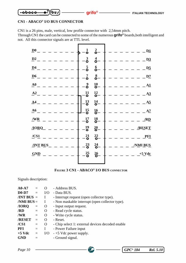
CN1 - ABACO® I/O BUS CONNECTOR
CN1 is a 26 pins, male, vertical, low profile connector with 2,54mm pitch.Through CN1 the card can be connected to some of the numerous grifo ® boards,both intelligent andnot. All this connector signals are at TTL level.
FIGURE 3 CN1 - ABACO® I/O BUS CONNECTOR
Signals description:
A0-A7 = O - Address BUS.D0-D7 = I/O - Data BUS./INT BUS = I - Interrupt request (open collector type)./NMI BUS = I - Non maskable interrupt (open collector type)./IORQ = O - Input output request./RD = O - Read cycle status./WR = O - Write cycle status./RESET = O - Reset./CS1 = O - Chip select 1: external devices decoded enablePFI = I - Power Failure input+5 Vdc = I/O - +5 Vdc power supply.GND = - Ground signal.
1 2
3 4
5 6
7 8
9 10
11 12
13 14
D0
D2
D4
D6
A0
A2
A4
D1
D3
D5
D7
A1
A3
A5
15 16
17 18
19 20
A6
/WR
/IORQ
A7
/RD
/RESET
21 22
23 24
25 26
/CS1
/INT BUS
GND
PFI
/NMI BUS
+5 Vdc

ITALIAN TECHNOLOGY grifo ®
Page 11 GPC® 184 Rel. 5.10
FIGURE 4: CARD PHOTO
FIGURE 5:COMPONENTS MAPS (SOLDERING SIDE AND COMPONENTS SIDE)

grifo ® ITALIAN TECHNOLOGY
Page 12 GPC® 184 Rel. 5.10
CN3A - SERIAL LINE A CONNECTOR
CN3A is a 6 pins, female PLUG connector for serial communication. Phisically, serial line A ofGPC® 184 board is connected to the ASCI 1 serial line of the CPU.Placing of the signal has been designed to reduce interference and electrical noise and to simplifyconnections with other systems, while the electric protocol follows the CCITT normative.
FIGURE 6: CN3A- SERIAL LINE A CONNECTOR
Signals description:
RXA RS 232 = I - Serial line A=ASCI1 RS 232 Receive Data.TXA RS 232 = O - Serial line A=ASCI1 RS 232 Transmit Data.CTSA RS 232 = I - Serial line A=ASCI1 RS 232 Clear To Send.RTSA RS 232 = O - Serial line A=ASCI1 (*1) RS 232 Request To Send.+5 Vdc/GND = - +5 Vdc power supply or ground signalGND = Ground signal
*1: The output handshake signal RTSA is not software manageable so it is kept continuoslydeactived = -10 Vdc. If this configuration is incompatible with the system to be connected,perform the connection without this signal.
+5 Vdc / GND GND TXA RS 232
RTSA RS 232 (*1) CTSA RS232
RXA RS 232
4 3 2 1 5 6

ITALIAN TECHNOLOGY grifo ®
Page 13 GPC® 184 Rel. 5.10
FIGURE 7: SERIAL COMMUNICATION DIAGRAM
Z180
DR
IVE
RS
RS 232
CN
3B
DRIVERS
RS 422RS 485
CURRENTLOOP
CN
3ASERIAL LINE A
SERIAL LINE B
AS
CI 1
AS
CI 0

grifo ® ITALIAN TECHNOLOGY
Page 14 GPC® 184 Rel. 5.10
CN3B - SERIAL LINE B CONNECTOR
CN3B is a 6 pins, female PLUG connector for serial line B, that can be buffered as RS 232, RS 422,RS 485 or Current Loop. Phisically, serial line B of GPC® 184 board is connected to the ASCI 0 serialline of the CPU. Placing of the signal has been designed to reduce interference and electrical noiseand to simplify connections with other systems, while the electric protocol follows the CCITTnormative.
FIGURE 8: CN3B- SERIAL LINE B CONNECTOR
Signals description:
RXB RS 232 = I - Serial line B=ASCI 0 RS 232 Receive Data.TXB RS 232 = O - Serial line B=ASCI 0 RS 232 Transmit Data.CTSB RS 232 = I - Serial line B=ASCI 0 RS 232 Clear To Send.RTSB RS 232 = O - Serial line B=ASCI 0 RS 232 Request To Send.RXB- RS 422 = I - Receive Data Negative: Serial line B=ASCI 0 negative signal for RS
422 serial differential receive.RXB+ RS 422 = I - Receive Data Positive: Serial line B=ASCI 0 positive signal for RS
422 serial differential receive.TXB- RS 422 = O - Transmit Data Negative: Serial line B=ASCI 0 negative signal for RS
422 serial differential transmit.TXB+ RS 422 = O - Transmit Data Positive: Serial line B=ASCI 0 positive signal for RS
422 serial differential transmit.
+5 Vdc / GNDGND
4 3 2 156
TXB RS 232 / TXB+ RS 422 /TXB- C.L.
RTSB RS 232 / TXB- RS 422 /TXB+ C.L.
CTSB RS232 / RXB- RS 422 /RXTXB- RS 485 / RXB- C.L.
RXB RS 232 / RXB+ RS 422 /RXTXB+ RS 485 / RXB+ C.L.

ITALIAN TECHNOLOGY grifo ®
Page 15 GPC® 184 Rel. 5.10
RXTXB- RS 485 =I/O-Receive Transmit Data Negative: Serial line B=ASCI 0 negativesignal for RS 485 serial differential receive and transmit.
RXTXB+ RS 485 =I/0- Receive Transmit Data Positive: Serial line B=ASCI 0 positive signalfor RS 485 serial differential receive and transmit.
RXB- C.L. = I - Receive Data Negative: Serial line B=ASCI 0 negative signal forCurrent Loop serial bipolar receive.
RXB+ C.L. = I - Receive Data Positive: Serial line B=ASCI 0 positive signal forCurrent Loop serial bipolar receive.
TXB- C.L. = O - Transmit Data Negative: Serial line B=ASCI 0 negative signal forCurrent Loop serial bipolar transmit.
TXB+ C.L. = O - Transmit Data Positive: Serial line B=ASCI 0 positive signal forCurrent Loop serial bipolar transmit.
+5 Vdc/GND = I - +5 Vdc or ground signal.GND = - Ground signal.
FIGURE 9: LEDS, CONNECTORS, MEMORIES , ETC. LOCATION
CN3B
P1
IC5RAM
CN5
CN3A
CN1
CN2
IC2ROM
BT1
LD1

grifo ® ITALIAN TECHNOLOGY
Page 16 GPC® 184 Rel. 5.10
FIGURE 10: RS 232 PIN OUT AND CONNECTION EXAMPLE
FIGURE 11: RS 422 PIN OUT AND POINT TO POINT CONNECTION EXAMPLE
FIGURE 12: RS 485 PIN OUT AND POINT TO POINT CONNECTION EXAMPLE
6 Ext
erna
l Sys
tem
CN
3A,B
GP
C®
184
GND GND
5
2
RXA, RXB
TXA, TXB RX
TX
4
3
CTSA, CTSB
RTSA, RTSB CTS
RTS
4
5
6
RXB -
RXB +
GND GND
TX +
TX -
Ext
erna
l Sys
tem
CN
3B G
PC
® 1
84
3
2
TXB -
TXB + RX +
RX -
4
5
6
RXTXB -
RXTXB +
GND GND
TX / RX +
TX / RX -
Ext
erna
l Sys
tem
CN
3B G
PC
® 1
84

ITALIAN TECHNOLOGY grifo ®
Page 17 GPC® 184 Rel. 5.10
FIGURE 13: RS 485 PIN OUT AND NETWORK CONNECTION EXAMPLE
TXRX +
-
GND
Master
120 Ω
GP
C®
184
Uni
t
TXRXB
+
-
Slave n
GND
+5V
TXRXB
+
-
GND
Slave 2
GP
C®
184
Uni
t
TXRXB
+
-
GND
Slave 1
GP
C®
184
Uni
t
grifo ® ITALIAN TECHNOLOGY
Page 18 GPC® 184 Rel. 5.10
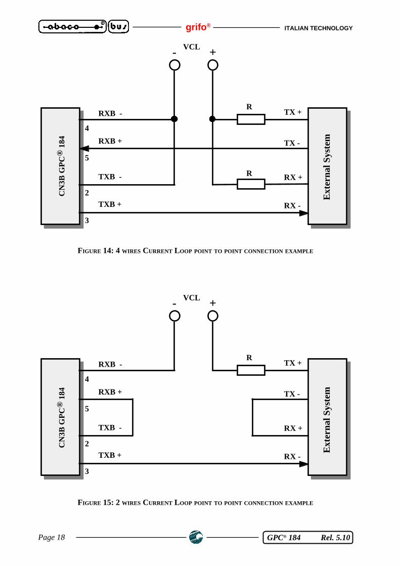
FIGURE 14: 4 WIRES CURRENT LOOP POINT TO POINT CONNECTION EXAMPLE
FIGURE 15: 2 WIRES CURRENT LOOP POINT TO POINT CONNECTION EXAMPLE
4
5
RXB -
RXB + TX -
TX +
Ext
erna
l Sys
tem
CN
3B G
PC
® 1
84
2
3
TXB -
TXB + RX -
RX +
- +VCL
R
R
4
5
RXB -
RXB + TX -
TX +
Ext
erna
l Sys
tem
CN
3B G
PC
® 1
84
2
3
TXB -
TXB + RX -
RX +
- +VCL
R

ITALIAN TECHNOLOGY grifo ®
Page 19 GPC® 184 Rel. 5.10
FIGURE 16: CN5 SIGNALS CONNECTION DIAGRAM
CN5
PIN 5
Z180
PIN 1
PIN 2
PIN 3
CS
I/O
CKS
RXS
TXS
PIN 6
PIN 4
/INT1
CKA1
CKA0
+5 Vdc

grifo ® ITALIAN TECHNOLOGY
Page 20 GPC® 184 Rel. 5.10
CN5 - AUXILIARY SIGNALS CONNECTOR
CN5 is 2.54 mm pitch, 5+5 pins, male, vertical, strip connector. CN5 is the interface for 3 signals ofthe synchronous serial communication, one /INT 1 interrupt signal, 2 baud rate generator signals andthe power supply. All signal are TTL.
FIGURE 17: CN5 - AUXILIARY SIGNALS CONNECTOR
Signals description:
CKS = I/O - Isochronous serial line clock signal.RXS = I - Isochronous serial line receive signal.TXS = O - Isochronous serial line transmit signal./INT1 = I - Interrupt request /INT1.CKA0 = I/O - ASCI 0 = serial B baud rate generator clock signal.CKA1 = I/O - ASCI 1 = serial A baud rate generator clock signal.+5 Vdc = O - +5 Vdc power supply.GND = - Ground signal.
1 2
+5VdcGND
3 4
CKA1/INT1 5 6
CKA0TXS
7 8
RXSCKS

ITALIAN TECHNOLOGY grifo ®
Page 21 GPC® 184 Rel. 5.10
I/O CONNECTION
To prevent possible connecting problems between GPC® 184 and the external systems, the user hasto read carefully the information of the previous paragraphs and he must follow these instrunctions:
- For RS 232,RS 422, RS 485 or Current Loop communication signals the user must follow thestandard rules of these protocols.
- For all TTL signals the user must follow the rules of this electric standard. The connected digitalsignal must be always referred to card digital ground. For TTL signals, the 0 Vdc level correspondsto logic state "0", while 5Vdc level corrisponds to logic state "1".
VISUAL SIGNALATIONS
GPC® 184 board is provided with a LED in order to signal to the User some internal status conditions,as described in the following table:
FIGURE 18: VISUAL SIGNALATIONS TABLE
The main purpose of this LED is to provide the User a visual indication of the board status, makingeasier the operations to verify the correct workig of the system. To easily locate the LED on the boardplease see figure 9, while for a description about the modalities of RTC interrupt generation pleaserefer to the paragraph "REAL TIME CLOCK".
LED COLOUR DESCRIPTION
LD1 RedIndicates the activation of the Real Time Clock interrupt requestsignal (/INT2 of the CPU).

grifo ® ITALIAN TECHNOLOGY
Page 22 GPC® 184 Rel. 5.10
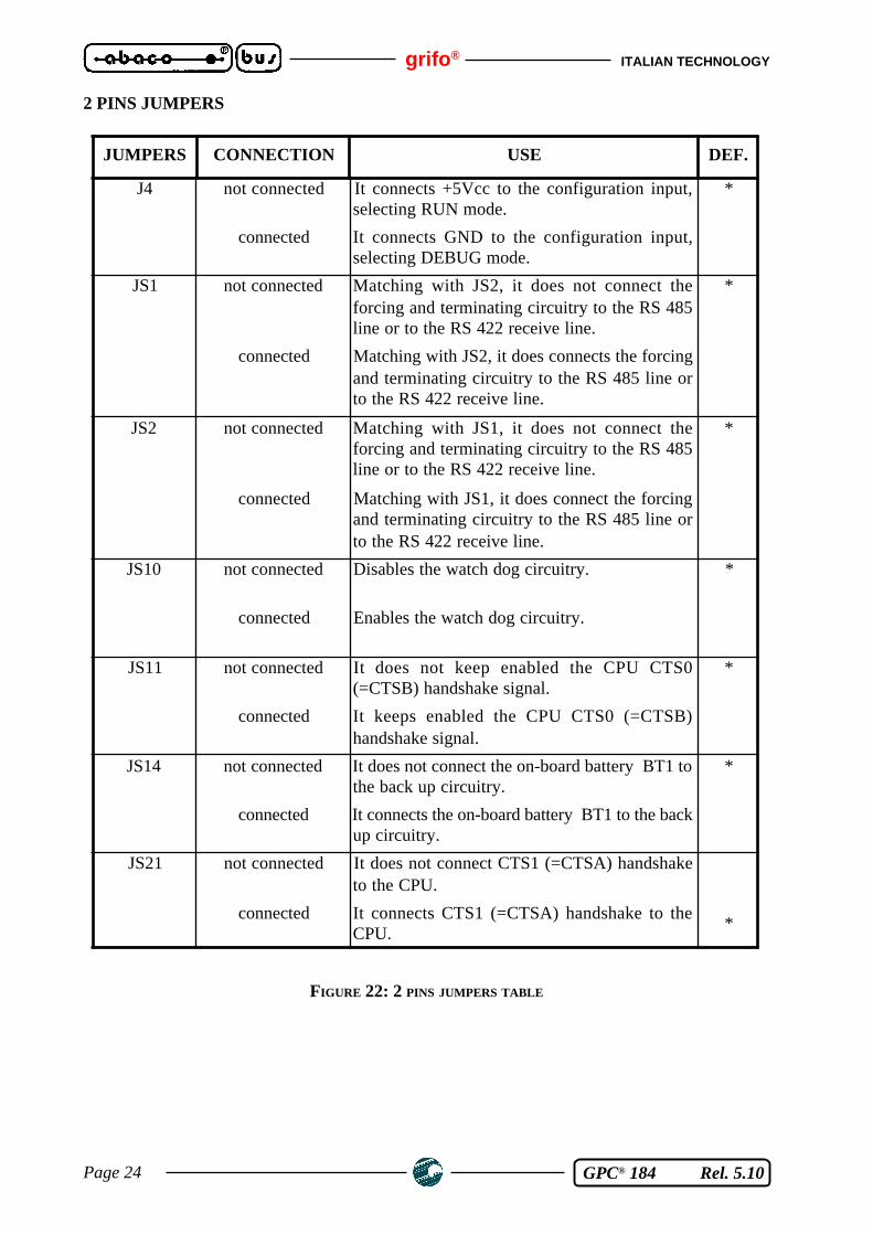
JUMPERS
On GPC® 184 there are 16 jumpers for card configuration, 9 of them are solder jumpers. Connectingthese jumpers, the user can define for example the memory type and size, the peripheral devicesfunctionality and so on. Below there is the jumpers list, location and function.
FIGURE 19: JUMPERS SUMMARIZING TABLE
The following tables describe all the right connections of GPC® 184 jumpers with their relativefunctions. To recognize these valid connections, please refer to the board printed diagram (serigraph)or to figure 5 of this manual, where the pins numeration is listed; for recognizing jumpers location,please refer to figures 20, 21. The "*" used in the following tables, denotes the default connection,or on the other hand the connection set up at the end of testing phase, that is the configuration the userreceives.
JUMPERS N. PIN FUNCTION
J1 3 It selects IC5 RAM size.
J2 3Matching with J3, it selects the device type, EPROM or FLASHEPROM, installed on IC2.
J3 3Matching with J2, it selects the device type, EPROM or FLASHEPROM, installed on IC2.
J4 2 It selects the configuration input (RUN or DEBUG).
J5 5 It selects between RS 422 and RS 485 for serial line B.
JS1 2Matching with JS2, it connects the termination and forcingcircuitry to the RS 485 line or to the RS 422 receive line.
JS2 2Matching with JS1, it connects the termination and forcingcircuitry to the RS 485 line or to the RS 422 receive line.
JS3 3 It selects the type of the connection for pin 1 of CN3A.
JS4 3 It selects the type of the connection for pin 1 of CN3B.
JS10 2 Activates the watch dog circuitry.
JS11 2 It keeps enabled the CPU CTSB handshake.
JS14 2 It connects the on board battery BT1 to the back up circuitry.
JS19 3 It selects which interrupt to connect to the power failure.
JS21 2 It selects the connection of the CTSA handshake.

ITALIAN TECHNOLOGY grifo ®
Page 23 GPC® 184 Rel. 5.10
FIGURE 20: JUMPERS LOCATION (COMPONENT SIDE)
FIGURE 21: JUMPERS LOCATION (SOLDERING SIDE)
J1
J4
J2
J3
J5
JS1
JS11
JS10
JS19
JS3
JS4
JS21
JS14
JS2
grifo ® ITALIAN TECHNOLOGY
Page 24 GPC® 184 Rel. 5.10
2 PINS JUMPERS
FIGURE 22: 2 PINS JUMPERS TABLE
JUMPERS CONNECTION USE DEF.
J4 not connected It connects +5Vcc to the configuration input,selecting RUN mode.
*
connected It connects GND to the configuration input,selecting DEBUG mode.
JS1 not connected Matching with JS2, it does not connect theforcing and terminating circuitry to the RS 485line or to the RS 422 receive line.
*
connected Matching with JS2, it does connects the forcingand terminating circuitry to the RS 485 line orto the RS 422 receive line.
JS2 not connected Matching with JS1, it does not connect theforcing and terminating circuitry to the RS 485line or to the RS 422 receive line.
*
connected Matching with JS1, it does connect the forcingand terminating circuitry to the RS 485 line orto the RS 422 receive line.
JS10 not connected Disables the watch dog circuitry. *
connected Enables the watch dog circuitry.
JS11 not connected It does not keep enabled the CPU CTS0(=CTSB) handshake signal.
*
connected It keeps enabled the CPU CTS0 (=CTSB)handshake signal.
JS14 not connected It does not connect the on-board battery BT1 tothe back up circuitry.
*
connected It connects the on-board battery BT1 to the backup circuitry.
JS21 not connected It does not connect CTS1 (=CTSA) handshaketo the CPU.
connected It connects CTS1 (=CTSA) handshake to theCPU.
*

ITALIAN TECHNOLOGY grifo ®
Page 25 GPC® 184 Rel. 5.10
3 PINS JUMPERS
FIGURE 23: 3 PINS JUMPERS TABLE
5 PINS JUMPERS
FIGURE 24: 5 PINS JUMPERS TABLE
JUMPERS CONNECTION USE DEF.
J1 position 1-2 It configures IC5 RAM for 128K. *
position 2-3 It configures IC5 RAM for 512K.
J2 position 1-2 It configures IC2 for FLASH EPROM, matchingwith J3.
position 2-3 It configures IC2 for EPROM, matching with J3. *
J3 position 1-2 It configures IC2 for FLASH EPROM, matchingwith J2.
position 2-3 It configures IC2 for EPROM, matching with J2. *
JS3 position 1-2 It connects pin 1 of CN3A to GND. *
position 2-3 It connects pin 1 of CN3A to +5 Vcc.
JS4 position 1-2 It connects pin 1 of CN3B to GND. *
position 2-3 It connects pin 1 of CN3B to +5 Vcc.
JS19 Not connected It does not connect the power failure circuitry. *
position 1-2 It connects the power failure circuitry to the CPU/INT0 signal.
position 2-3 It connects the power failure circuitry to the CPU/NMI signal.
JUMPERS CONNECTION USE DEF.
J5 not connected It selects the RS 232 protocol for serial line B. *
position 1-2 and 3-4 It selects the RS 485 (half duplex 2 wires) forserial line B.
position 2-3 and 4-5 It selects the RS 422 (full duplex or half duplex4 wires) for serial line B.

grifo ® ITALIAN TECHNOLOGY
Page 26 GPC® 184 Rel. 5.10
BACK UP
GPC® 184 ha an on board lithium battery BT1 for the back up of RAM and RTC content when powersupply is switched off. Jumper JS14 connects phisically the battery so it can be disconnected to saveits duration whenever back-up is not needed. By CN2 connector itis possible to connect an externalbattery: configuration of jumper JS14 does not affect the working of this battery and it can replaceBT1 completely.Please refer to the paragraph “ELECTRIC FEATURES” to choose the type of the external back upbattery, to easily locate see figure 9.
MEMORY SELECTION
On GPC® 184 can be mounted up to 1024K bytes of memory divided in several configurations, asdescribed in the following table:
FIGURE 25: MEMORY SELECTION TABLE
All the above mentioned devices must follow the JEDEC pin out specifications. Fo furtherinformations about the signatures of the component that can be mounted please refer to themanifacturers documentations. To easily locate the memory devices please refer to figure 9.The default configuration of the GPC® 184 board memory is only 128K RAM; any different memoryconfiguration can be realized by the User by mounting the opportune devices or can be requested inthe ordering phase. Here follow the codes to order the optional memoy configurations:
.512 -> 512K RAM
For further informations about prices and options please contact grifo ®.
IC DEVICE SIZE JUMPERS CONNECTION
2 EPROM 128K Byte J2, J3 position 2-3
EPROM 256K Byte J2, J3 position 2-3
EPROM 512K Byte J2, J3 position 2-3
FLASH EPROM 128K Byte J2, J3 position 1-2
FLASH EPROM 512K Byte J2, J3 position 1-2
5 RAM 128K Byte J1 position 1-2
RAM 512K Byte J1 position 2-3
ITALIAN TECHNOLOGY grifo ®
Page 27 GPC® 184 Rel. 5.10
INTERRUPTS
One of the most important GPC® 184 features is the powerful interrupts management. Here is a shortdescription of how the board's hardware interrupt signals can be managed; a more completedescription of the hardware interrupts can be found in the microprocessor data sheets or in AppendixB of this manual.
- ABACO® I/O BUS -> It generates an /NMI interrupt, by the /NMI BUS signal of CN1connector.It generates an /INT0 non vectored interrupt, by the /INT BUS signalof CN1 connector.
- Real Time Clock -> It generates an /INT2 vectored interrupt.- Auxiliary signals -> It generates an /INT1 vectored interrupt, by the homonymous CN5
signal.- Power failure -> It generates an /NMI interrupt or an /INT0 non vectored interrupt.- CPU inside devices -> They generate a vectored interrupt. Possible sources of internal
interrupt events are: PRT 0, PRT 1, DMA 0, DMA 1, CSI/O, ASCI 0,ASCI 1.
The board features a chained priority structure that manages the case of contemporary interrupts. Theaddresses of the response procedures for vectored interrupts can be software programmed by the Useracing on microprocessor inside registers. So the user program has always the possibility to reactpromptly to every external event, deciding also the priority of interrupts.
CONFIGURATION INPUTS
GPC® 184 board is provided with one jumper (J4), tipically used for system configuration purposes,that can be software acquired by the user program. The mostly implemented applications for thisfeature are: working conditions setting, selection of some on-board firmware parameters, etc. Theconfiguration of the jumper generates a signal in complemented logic (0 -> means jumper connected1 -> means jumper disconnected) that can be read performing a read operation atthe address assignedto the jumper by the on board control logic. Some software tools use this jumper for the selectionbetween the RUN and DEBUG working modalities. For further informations please refer to theparagraph "I/O ADDRESSES", while to easily locate the jumper on the board please refer to figure20.
SOLDER JUMPERS
The solder jumpers called JSxx are connected by a thin copper connection on the solder side. So, ifone of their configurations has to be changed, the User must first cut this connection using asharpened cutter, then make the new connection using a low power soldering tool and some non-corrosive tin.

grifo ® ITALIAN TECHNOLOGY
Page 28 GPC® 184 Rel. 5.10
SERIAL COMMUNICATION SELECTION
The communication serial line A is always buffered in RS 232 while the serial line B can be bufferedin RS 232, RS 422, RS 485 or current loop electric standard. By hardware can be selected which oneof these electric standard is used, through jumpers connection (as described in the previous tables).By software the serial lines can be programmed to operate with 7, 8, 9 bits per character, parity,between 1 and 2 stop bits at standard or no standard baud rates, through some CPU internal registersetting.Some components necessary for RS 422 and RS 485 communication are not mounted and not testedon the default configuration card, so the first not standard configuration must always be executed bygrifo ® technician; then the user can change himself the configuration, following the belowdescription:
- SERIAL LINE B=ASCI 0 CONFIGURED IN RS 232 (default configuration)IC9 = MAX 202 driver
J5 = not connected IC10 = no componentJS1, JS2 = not connected IC11 = no componentJS11 = not connected IC12 = no component
IC13 = no component
- SERIAL LINE B=ASCI 0 CONFIGURED IN CURRENT LOOP (.CLOOP option)IC9 = no component
J5 = not connected IC10 = no componentJS1, JS2 = not connected IC11 = HP 4200 driverJS11 = connected IC12 = no component
IC13 = HP 4100 driverThe current loop serial line is a passive line, so during connection the user must provide anexternal power supply, as described in figures 14 and 15. The current loop interface allowseither point to point or network connection with 4 or 2 wires.
- SERIAL LINE B=ASCI 0 CONFIGURED IN RS 422 (.RS422 option)IC9 = no component
J5 = position 2-3, 4-5 IC10 = SN 75176 driverJS1, JS2 = (*) IC11 = no componentJS11 = connected IC12 = SN 75176 driver
IC13 = no componentWith /RTSB=/RTS0 signal (managed by software with ASCI 0 registers) the user enables ordisables the transmitter driver:
/RTS0 = low level = 0 logic state -> transmitter driver enabled/RTS0 = high level = 1 logic state -> transmitter driver disabled
allowing either point to point (driver can be mantained always enabled) or network (driver isenabled only when the unit can hold the line) connection.

ITALIAN TECHNOLOGY grifo ®
Page 29 GPC® 184 Rel. 5.10
Serial B = ASCI 0 in RS 232 Serial B = ASCI 0 in current loop
Serial B = ASCI 0 in RS 422 Serial B = ASCI 0 in RS 485
FIGURE 26: SERIAL COMMUNICATION DRIVER LOCATION
MAX 202
MA
X 2
02
HP4200
HP4100
MA
X 2
02
SN75176
SN75176
MA
X 2
02
SN75176
MA
X 2
02

grifo ® ITALIAN TECHNOLOGY
Page 30 GPC® 184 Rel. 5.10
- SERIAL LINE B=ASCI 0 CONFIGURED IN RS 485 (.RS485 option)IC9 = no component
J5 = position 1-2, 3-4 IC10 = no componentJS1, JS2 = (*) IC11 = no componentJS11 = connected IC12 = SN 75176 driver
IC13 = no componentWith /RTSB=/RTS0 signal (managed by software with ASCI 0 registers) the user defines theRS 485 line direction:
/RTS0 = low level = 0 logic state -> RS 485 line transmitting/RTS0 = high level = 1 logic state -> RS 485 line receiving
allowing network connection in a master multi slave system and multi master system. With RS485 communication line, on CN3B the pins 4 and 5 have the double function of reception andtransmission signals. All the transmitted characters are at the same time received when the userselect RS 485 on GPC® 184; in this way the line conflicts can be immediately recognized bysimply testing the received character after each transmission.
(*) With jumper JS1 and JS2 the RS 422 receiving line or the RS 485 line can be terminated andforced with a suitable resistors circuit. The line termination must be added only at the beginningand at the end of the physical line, connecting both the jumpers. Normally these jumper mustbe connected in point to point network, or on the farther cards in multipoints network.
After reset or power on phase, the /RTS0 signal is forced to high level that mantain the RS 485 driverreceiving and that disables the RS 422 transmitter driver; this condition eliminates any conflict onthe communication line.
- SERIAL LINE A=ASCI 1The output handshake signal RTSA is not software manageable so it is kept continuoslydeactived = -10 Vdc. If this condition is incompatible with the system to be connected, performthe connection without this signal.The JS21 jumper connects the handshake signal CTSA, converted by proper RS 232 driver,to CPU signal /CTS1. This last signal has a double functionality and it can work also as RXS,if the syncronous serial line available on CN5 is used, the JS21 jumper must be disconnected.
For further information about serial communication, please refer to connection examples describedin figures 10÷13.
RESET AND WATCH DOG
The watch dog circuit of GPC® 184 is really efficient and provided of easy software management.In details the most important features of this circuit are:- astable functionality;- intervent time of about 1,5 sec;- hardware enable;- software retrigger;With the astable mode when the intervent time elapses, the circuit becomes active, it stay active tillthe end of reset time (about200 msec) and after it is deactivated. Jumper JS10 connects the watch dog

ITALIAN TECHNOLOGY grifo ®
Page 31 GPC® 184 Rel. 5.10
circuit to reset circuit so when it is connected the watch dog is enabled and viceversa. The watch dogretrigger operation is described in chapter "WATCH DOG".After an activation and following deactivation of /RESET signal, the card resumes execution of theprogram saved on IC2 (at address 0000H) starting from a global reset status of all the on boardperipheral devices.Please remember that the /RESET signal is connected to CN1 connector and that on GPC® 184 areavailable other reset sources as the power good circuit and the contact P1. The two pins of P1 canbe connected to a normally open contact (i.e. a push button) and when the contact is closed (shortcutof the two pins) the reset circuit is enabled.
POWER FAILURE
Together with the power management circuit of the CPU, it is also available an interesting powerfailure circuit, that can be connected to two different interruptsignals (/NMI or /INT0).The power failure circuit checks the voltage connected to PFI pin of CN1 and whenever it reachesthe threshold intervent value (1,25V), it enables its output and it captures CPU attention if JS19 isconnected.The common use of this circuit is to inform application program of the imminent power supplyfailure, so as to save the necessary status information. The PFI signal can be connected withadvantages to power supply voltage through a dedicated resistors network; this one must provide thethreshold intervent voltage with a sufficient advance in confront of /RESET activation. This advancemust hold out to the end of interrupt service routine, so the resistors network values must be selectedaccording with used power supply voltage, residue capacitor charge and interrupt service executiontime.
grifo ® ITALIAN TECHNOLOGY
Page 32 GPC® 184 Rel. 5.10
SOFTWARESOFTWARE
A wide selection of software development tools can be obtained, allowing use of the module as asystem for its own development, both in assembler and in other high level languages; in this waythe User can easily develop all the requested application programs in a very short time. Generallyall software packages available for the mounted microprocessor, or for the Z80 and Z180 family,can be used, i.e.:
GET 80It is a complete program with Editor, Communication driver, and Mass Memory management for allZ80 family cards. This program, developed by grifo ®, allows to operate in the best conditions whenGDOS, FGDOS or xGDOS MCI software tools are used; GET 80 is supplied when one of thesetools is ordered and it is personalized with name and general data of the customer. A useful list ofpull down menus and the possibility of using mouse, make program use very comfortable. GET 80program can be executed both on MS-DOS system and on MACINTOSH computers too, throughSOFT-PC program. It is supplied on MS-DOS 3”1/2 floppy disk with the documentation on GDOS80 manual.
GDOS 184It is a complete development Tool for GPC® 184 card. It is supplied together with GET 80 programto allow an easy and immediate use of this powerful development system. GDOS is divided in twodifferent structures : the first one works on PC maintaining serial communication with the secondone. The second structure is on EPROM, it works on board of the card and it is an efficient operatingsystem that executes many low level functions and, at the same time, it allows high level languageuse. The combination of the said structures results in a complete machine, in fact the card uses PCresources (like floppy disk, hard disk, printer, keyboard, monitor, etc.) as its own peripheral devices.This resulting “virtual machine” performs operation in a transparent way for the User, so this lattercan operate with the same modality of standard PC languages. It is really interesting the compatibilityof GDOSwith all CP/M program and languages; so, if the User has experience, knowledge ordeveloped applications with CP/M, he can use immediately GDOS, without any changes.Moreover, GDOS can manage all memory devices exceeding 64K Bytes as RAM disk and ROMdisk. The on board RAM devices can directly be used performing data read and write operations withthe confortable file formats.This software tools is supplied on EPROM with MS-DOS GET 80 floppy disk, some examples,utilities and the operating system documentation.
FGDOS 184It is really similar to GDOS, but it can program and erase the on board FLASH EPROM with theapplication program developed from the User. In this way the external EPROM programmer is notnecessary to store definitely the program and it is possible to modify or to add code directly on theinstalled machine, through a portable PC.This software tools is supplied on FLASH EPROM with MS-DOS GET 80 floppy disk, someexamples, utilities and the operating system documentation.

ITALIAN TECHNOLOGY grifo ®
Page 33 GPC® 184 Rel. 5.10
xGDOS MCI 184It is a version of GDOS or FGDOS sofware tools, capable of PCMCIA Memory Card management.Using MCI 64 card, the GDOS operating system manages memory cards as RAM disk or ROM disk.All applications with data acquisition and data logging can be realized with high level languages thatmanage data on files, with a fast development time and without any software complication.This software tool is supplied on EPROM or FLASH EPROM with MS-DOS GET 80 floppy disk,some examples, utilities and the operating system documentation.
PASCAL 80It is an efficient and complete PASCAL Compiler for Z80 family cards, with features similar toRelease 3.0 of Borland Turbo PASCAL . It must work together with any GDOS version and it canexceed the 64K memory limits of Z80 family microprocessors through OVERLAY modality. Morethan one application program can be saved in RAM and/or ROM disks and subsequently executed.The terminal emulation of GET 80 program support the typical full screen PASCAL Editor,including the attributes management.This program is supplied as ROM DISK file in GDOS EPROM or FLASH EPROM and on MS-DOS floppy disk with some example and manual.
HI TECH C 80Professional C Cross Compiler of Hi-Tech Software Inc. This Compiler is terribly fast and itgenerates a small quantity of code. This result is due to advanced techniques in optimizing thegenerated code based on Artificial Intelligence techniques which allow to get a very compact andvery fast code. The package includes: IDE, Compiler, Code optimizer, Assembler, Linker, RemoteDebugger and so on. This tool is Full ANSI/ISO Standard and Full Library Source Code. Once theporting of the Remote-Debugger module is done, this tool allows the user the software debuggingdirectly on the hardware that he is experimenting. This type of specilization of the Remote Debuggeris available from now ant it is supplied with all grifo ® CPU cards. This software package is on 3”1/2 diskettes under MS-DOS format along with user manual. This version supports these followingCPUs: Z80, Z180, 84C011, 84C11, 84C013, 80C13, 84C015, 84C15, 64180, NCS800, Z181, Z182.
DDS MICRO C 85: low cost ross compiler for C source program. It is a powerful software tool thatincludes editor, C compiler (integer), assembler, optimizer, linker, library, and remote debugger, inone easy to use integrated development environment. There are also included the library sources andmany utilities programs.
NOICE : It is a PC hosted debugger consists of a target specific DOS program, NOICExxx.EXE, anda target resident monitor program. The two programs comunicate via RS 232. NOICE includes:source level debug; a disassembler; a file viewer; memory display and editing; a virtually unlimitednumber of breakpoints; hardware free single step; definition of symbols; the ability to record and playback files of commands; on line help.
grifo ® ITALIAN TECHNOLOGY
Page 34 GPC® 184 Rel. 5.10
RSD 184This software tools is a Remote Symbolic Debugger with two operating mode. The first one is amonitor debugger modality with software emulation on P.C.; the second is a remote monitordebugger modality that execute code directly on the card. Trough serial communication the User can:down load an HEX file and associated symbol table, debug code in symbolic mode, execute code instep to step mode or in real time mode, set breakpoint, dump and modify memory and registers, etc.RSD software tool supports both Z80 and Z180 instrunction sets. Really interesting is the programexecution management, in fact many hardware and software breakpoint are supported. RSD can beused together with assembler tools, like ZASM 80, and C Compiler CC 80.It is supplied on EPROM and on MS-DOS floppy disk with technical manual.
ZASM 80It is a macro cross assemler that operates on any PC with MS-DOS operating system. It supports bothZ80 and Z180 instruction sets. The generated code can be debugged on PC, through softwaresimulation, or directly on target card, through remote modality, using RSD software tools. ZASM80 is compatible with C Compiler CC 80 of which it assemble the compilation result.It is supplied on MS-DOS floppy disk with technical manual.
CC 80It is a complete C Compiler with ANSI/ISO standard, provided of floating point procedure, that cangenerate code for Z80 and Z180 family microprocessors. It works together with cross assemblerZASM 80 and Symbolic Debugger RSD.It is supplied on MS-DOS floppy disk with technical manual.
EMBEDDED PASCAL Z80 - Z180Cross compiler for PASCAL source program. It is a powerful software tool that includes editor,PASCAL compiler, assembler, optimizer, library, included in an easy to use integrated developmentenvironment for Windows 95 and NT. Many memory models and data types are supported andsources of library are provided too.
ITALIAN TECHNOLOGY grifo ®
Page 35 GPC® 184 Rel. 5.10
DEVICES MAP AND ADDRESSESDEVICES MAP AND ADDRESSES
INTRODUCTION
In this chapter are reported all informations about card use, related to hardware features ofGPC® 184. For example the registers addresses, the memory and peripheral devices allocation aredescribed below.
ON BOARD DEVICES ADDRESSES
The on board devices addresses are managed from a control logic, realized with CMOS gates. Thiscontrol logic allocates memory and peripheral devices with very low power consumption and simplesoftware management.The control logic has been designed to control the memory and the I/O peripherals addresses in aseparate manner. The Z180 microprocessor directly addresses 64K bytes of memory and 256 I/Oregisters and the control logic provides on board memory and peripheral devices allocattion insidethese addresses spaces. The maps management is completely driven by software through the MMUcircuit programmation: the used memory can be selected and divided in some size definiblesegments. About I/O maps the control logic avoids every conflicts problems between CPU internaland external peripherals.Summarizing the control logic allocates:
- ABACO® I/O BUS- Up to 512K bytes of EPROM or FLASH EPROM on IC 2- Up to 512K of RAM on IC 5- Configuration jumper J4- Real Time Clock- Watch dog circuit
The addresses of all these devices are described in the following paragraphs and can't be set withdifferent values. If some different specific maps are required, please contact directly grifo ®.
ABACO ® I/O BUS ADDRESSES
The GPC® 184 control logic defines ABACO® I/O BUS addresses and only these addresses mustbe used to manages correctly the BUS. As described in following "I/O ADDRESSES" table, only theaddresses from 80H to FFH are available for ABACO® I/O BUS. Any I/O operations at each one ofthese adrresses enables the /IORQ signal and the other control signals of CN1 connector. In theaddresses subrange 80H÷9FH it is also enabled the /CS1 signal, used for external peripheral devicescoded selection.

grifo ® ITALIAN TECHNOLOGY
Page 36 GPC® 184 Rel. 5.10
MEMORY ADDRESSES
The maximum 1024K bytes of memory, are allocated on the board as below described:
- Up to 512K bytes of EPROM or FLASH EPROM allocated in memory space.- Up to 512K bytes of RAM allocated in memory space.
GPC® 184 can directly manage no more than 64K bytes of memory that is the microprocessor logicaddressable space. On the board this logic space can be divided in three separated segments: eachones of these segment have software programmable dimension and start address. The CPU internalMMU circuit divides the logical space directly managed by the microprocessor into these 3 segmentsand it allocates them in the physical memory devices space. The MMU circuit is softwareprogrammable with I/O operations to three specific registers in a fast and comfortable manner. SoMMU allows software managements of a physical memory space very larger than microprocessormemory space.The following figure describe available memory configurations; for further informations on MMUuse and segments meaning (Common Area 0, Common Area 1 and Bank Area), please refer toappendix B, while for memory devices location and configuration refer to figures 9 and 25.After power on or reset phase, the MMU circuit allocates all the logical 64K space at the beginningof the physical space, therefore the card starts execution of code saved at address 0000H of EPROMor FLASH EPROM on IC2.
The memory size and type configurations must be selected both according to used software tools andUser requests and/or application features. The card configuration for the selected memory devicetypes and sizes on IC2 and IC5 sockets, is performed with some comfortable jumpers, as describedin "MEMORY SELECTION" chapter.
Some software tools, i.e. GDOS, self manage the MMU circuit to use all the available memories athigh level witout User intervention.

ITALIAN TECHNOLOGY grifo ®
Page 37 GPC® 184 Rel. 5.10
FIGURE 27: MEMORY ALLOCATION
I/O ADDRESSES
The on board control logic manages the allocation of all the peripheral devices registers in themicroprocessor I/O space, that is 256 bytes long. Next table shows names, addresses, meanings anddirections of peripheral device registers (including the internal microprocessor ones). For a detaileddescription of the registers function, please refer to next chapter "PERIPHERAL DEVICESSOFTWARE DESCRIPTION".
FFFFFH
RAM
IC 5
80000H
7FFFFH
00000H
EPROM / FLASH
IC 2
4÷64 KBytes
COMMON Area 0
BANK Area
COMMON Area 1
4÷64 KBytes
4÷64 KBytes

grifo ® ITALIAN TECHNOLOGY
Page 38 GPC® 184 Rel. 5.10
FIGURE 28: I/O ADDRESSES TABLE
DEVICES REG. ADDRESS R/W FUNCTION
ASCI ASCI 00H÷09H R/WInternal microprocessor registers, forasyncronous serial line
CSI/O CSIO 0AH÷0BH R/WInternal microprocessor registers, forClocked Serial I/O Port management
TIMER TMR 0CH÷1FH R/WInternal microprocessor registers, forTimer/Counter management
DMA DMA 20H÷32H R/WInternal microprocessor registers, for DMAlines management
INTERRUPT INT 33H÷35H R/WInternal microprocessor registers, forinterrupts management
REFRESH RCR 36H÷37H R/WInternal microprocessor registers, forRefresh circuit management
MMU MMU 38H÷3AH R/WInternal microprocessor registers, forMemory Management Unit management
I/O ICR 3BH÷3FH R/WInternal microprocessor registers, for I/Ocontrol management
REAL SEC1 40H R/W Data register for seconds units
TIME SEC10 41H R/W Data register for seconds decinesCLOCK MIN1 42H R/W Data register for minutes units
MIN10 43H R/W Data register for minutes decinesHOU1 44H R/W Data register for hours units
HOU10 45H R/W Data register for hours decines and AM/PMDAY1 46H R/W Data register for day unitsDAY10 47H R/W Data register for day decinesMON1 48H R/W Data register for month units
MON10 49H R/W Data register for month decinesYEA1 4AH R/W Data register for year units
YEA10 4BH R/W Data register for year decinesWEE 4CH R/W Data register for week day
REGD 4DH R/W Control register DREGE 4EH R/W Control register EREGF 4FH R/W Control register F
C. JUMPER RUNDEB 60÷7FH RRegister for configuration jumperacquisition
W. DOG RWD 60÷7FH R Register for watch dog retrigger
ABACO® /CS1 80H÷9FH R/WABACO® I/O BUS addresses that enable/CS1 signal
I/O BUS I/OBUS 80H÷FFH R/W ABACO® I/O BUS addresses
ITALIAN TECHNOLOGY grifo ®
Page 39 GPC® 184 Rel. 5.10
PERIPHERAL DEVICES SOFTWARE DESCRIPTIONPERIPHERAL DEVICES SOFTWARE DESCRIPTION
In the previous paragraphes are described the external registers addresses, while in this one there isa specific description of registers meaning and function (please refer to I/O addresses table, for theregisters names and addresses values). For a more detailed description of the devices, please referto manufacturing company documentation; for microprocessor internal peripheral devices, notdescribed in this paragraph, refer to appendix B. In the following paragraphs the D7÷D0 indicationdenotes the eight bits of the combination used in I/O operations.
REAL TIME CLOCK
This peripherial is allocated in 16 consecutives I/O addresses, 3 of which correspond to statusregistres while the remaining 13 are for datas. Data registers are used both for read operations (of thecurrent time and date) and write operations (to initialize the time and date) just like the status registerswhich are used in write operations (to program the operative mode) and in read operations (to acquirethe RTC status). Here follows a list of the RTC data registers' meanings:
SEC1 - Units of seconds - 4 least significant bits of SEC1.3÷SEC1.0SEC10 - Decines of secondi - 3 least significant bits of SEC10.2÷SEC10.0MIN1 - Units of minutes - 4 least significant bits of MIN1.3÷MIN1.0MIN10 - Decines of minutes - 3 least significant bits of MIN10.2÷MIN10.0HOU1 - Units of hours - 4 least significant bits of HOU1.3÷HOU1.0HOU10 - Decines of hours - 2 least significant bits of HOU10.1÷HOU10.0
The third bit of HOU10.2 indicates AM/PMDAY1 - Units of day number - 4 least significant bits of DAY1.3÷DAY1.0DAY10 - Decines of day number - 2 least significant bits of DAY10.1÷DAY10.0MON1 - Units of month - 4 least significant bits of MON1.3÷MON1.0MON10 - Decines of month - 1 least significant bit of MON10.0YEA1 - Units of year - 4 least significant bits of YEA1.3÷YEA1.0YEA10 - Decines of year - 4 least significant bits of YEA10.3÷YEA10.0WEE - Day of the week - 3 least significant bits of WEE.2÷WEE.0
For this last register the three least significant bits mean:
WEE.2 WEE.1 WEE.0 Day of the week0 0 0 Sunday0 0 1 Monday0 1 0 Tuesday0 1 1 Wednesday1 0 0 Thursday1 0 1 Friday1 1 0 Saturday
The meaning of the three control registers is:

grifo ® ITALIAN TECHNOLOGY
Page 40 GPC® 184 Rel. 5.10
bit 7 6 5 4 3 2 1 0REG D = NU NU NU NU 30S IF B Hwhere:NU = Not used.30S = If high (1) itallowes a 30 seconds correction of the time. Once set the RTC seconds are
reset and the minutes increased, if the previous seconds was equal or greater than 30.IF = It manages the RTC interrupt status. When read it shows the current interrupt status (1
active and viceversa), when reset to 0 it disables the RTC interrupt signal if the interruptmode is selected.
B = Indictes whether R/W operations can be performed on the registers:1 -> operations are not permitted and viceversa.
H = If high (1) it stores the written time and date.
bit 7 6 5 4 3 2 1 0REG E = NU NU NU NU T1 T0 I Mwhere:NU = Not used.T1 T0 = Determin the duration of the internal counters interrupt cycle. 0 0 -> 1/64 second 0 1 -> 1 second 1 0 -> 1 minute 1 1 -> 1 hourI = It defines the interrupt operating mode:
1 -> it selects interrupt mode: when the selected duration elapses the interrupt isenabled and then disabled only with a reset of bit IF of control register D;
0 -> it selects the standard mode: when the selected duration elapses the interruptis enabled and then disabled only after 7,8 msec.
M = It mask the interrupt status:1 -> interrupt masked: the RTC interrupt signal is always disabled;0 -> interrupt not masked: the RTC interrupt signal reflects interrupt status.
bit 7 6 5 4 3 2 1 0REG F = NU NU NU NU T 24/12 S Rwhere:NU = Not used.T = It determines from which internal counter to take the counting signal:
1 -> main counter (fast counter for test);0 -> 15th counter.
24/12 = It determines the hours counting mode:1 -> 0÷23;0 -> 1-12 with AM/PM.
S = If high (1) it stops the clock time counting until the next enabling (0).R = If high (1) it resets all the internal counters.

ITALIAN TECHNOLOGY grifo ®
Page 41 GPC® 184 Rel. 5.10
WATCH DOG
Retrigger operation of GPC® 184 watch dog circuit is performed with a simple read operation at theaddress of register RWD. This register shares the same address of other on board peripherals, but noconflict are generated in fact retrigger operation is an input operation and the read data has nomeaning. To avoid watch dog activation it is necessary to retrigger its circuit at regular time periodsand the duration of these periods must be smaller than intervent time. If retrigger doesn't happen asbefore described and JS14 is connected, when intervention time is elapsed, the card is reset. Thedefault intervention time is about 1.5 sec.
CONFIGURATION JUMPER
The J4 configuration jumper installed on the GPC® 184 board can be acquired simply by performinga read operation from RUNDEB registers and masking bit D7. The value is in complemented logic,this means that the connected jumper gives a logic value "0" while if the jumper is not connected thelogic value read will be "1".This jumper switches between theRUN (not connected) or the DEBUG (connected) mode, a featureused by some grifo ® software tools.
CPU INTERNAL PERIPHERALS
The decriptions of the registers that manages the CPU internal peripheral devices (ASCI, CSI/O,TIMER, DMA, INTERRUPT, REFRESH, MMU, I/O) is available in the appendix B. Whenever thisinformations are still insufficient, please refer to specific documentation of the manufacturingcompany.
grifo ® ITALIAN TECHNOLOGY
Page 42 GPC® 184 Rel. 5.10
EXTERNAL CARDSEXTERNAL CARDS
GPC® 184 can be connected to a wide range of block modules and operator interface systemproduced by grifo ®, or to many system of other companies.The on board resources can be expandedwith a simple connection to the numerous peripheral grifo ® boards,both intelligent and not, thanksto its standard ABACO® I/O BUS connector. Even single EURO cards with BUS ABACO® can beconnected, by using the proper mother boards.Hereunder some of these cards are briefly described; ask the detailed information directly to grifo ®,if required.
QTP G26Quick Terminal Panel - LCD Graphic, 26 keys
Intelligent user panel equipped with graphic LCD display 240x128 pixel, CFC backlit; optocoupledRS 232 line and additional RS 232, RS 422, RS 485 or current loop serial line. Indipendent optionalCAN line controller; serial E2 for set up; RTC and RAM Lithium backed; primary graphic objects;possibility of renaming keys, LEDs and panel name by inserting label with new name into the properslot; 26 Keys and 16 LEDs with blinking attribute and buzzer manageable by software; built in powersupply; reader of magnetic badge, smart card and relay option.
ADC 812Analog to Digital Converter, 12 bits, multi range
DAS (Data Acquisition System) multi range 8 channels 12 bit A/D conversion lines; track and hold;6µs conversion time; range ±10, ±5, +10, +5Vdc or 0÷20, 4÷20mA; analog inputs connectionsthrough quick terminal screw connectors; ABACO ® I/O BUS interface; direct mounting for DIN247277-1 and 3 rails; 4 type dimension.
DAC 212Digital to Analog Converter 12 bits, multi range
Digital to Analog converter; multi range 2 channels 12 bits ± 10, +10 Vdc output; analog outputsconnections through quick terminal screw connectors; ABACO ® I/O BUS interface; direct mountingfor DIN 247277-1 and 3 rails; 4 type dimension.
CAN 14Control Area Network, 1 channel, galvanically insulated
UART CAN SJA1000; 1 serial channels galvanically insulated; ABACO® I/O BUS interface; 4 typedimension; support of CAN 2.0B protocol; transfer rate up to 1M bit/sec; direct mounting for DIN247277-1 and 3 rails.
ETI 324Encoder Timer I/O, 3 counters, 24 I/O
Three timers counters driven by 82C54; bidirectional optocoupled encoder input; direction identifier;phases multiplier; 24 digital lines driven by 82C55 on two standard I/O ABACO® connectors;ABACO® I/O BUS interface; direct mounting for DIN 247277-1 and 3 rails; 4 type dimension.
ABB 05ABACO® Block BUS 5 slots
5 slots ABACO® mother board with power supply. Double power supply built in; 5Vdc 2,5A sectionfor powering the on board logic; second section at 24Vdc 400mA galvanically coupled, for theoptocoupled input lines. Auxiliary connector for ABACO® I/O BUS. Connection for DIN Ω rails.

ITALIAN TECHNOLOGY grifo ®
Page 43 GPC® 184 Rel. 5.10
PC
like
or
Mac
into
shP
L C
QT
P G
26P
C li
ke o
rM
acin
tosh
QT
P G
26
EX
TE
RN
AL
LIT
IUM
BA
TT
ER
Y3,
6 V
+ -
1 H
ardw
are
Ser
ial
Line
RS
232
, R
S 4
22, R
S 4
85, C
urre
nt L
oop
AB
AC
O®
I/O
BU
S
AB
B 0
3 or
AB
B 0
5, e
tc.
ZB
x se
ries
CI/O
R16
-T16
, etc
.
IPC
52,
UA
R 2
4, e
tc.
AN
Y I/
O T
YP
E
ABACO® BUS
1 H
ardw
are
Ser
ial
Line
RS
232
QT
P 2
2
P L
C
CO
NN
EC
TIO
N T
O Q
TP
24P
,Q
TP
16P
, KD
x x
xx, M
CI 6
4, e
tc.
882c
5582
C55
ME
MO
RIE
S, S
HIF
T
RE
GIS
TE
Rs,
PE
RIP
HE
RA
LS,
or a
ny d
evic
es w
ithsy
ncro
nous
ser
ial i
nter
face
(CS
I/O, S
PI,
Mic
row
ire, e
tc.)
FIGURE 29: AVAILABLE CONNECTIONS DIAGRAM

grifo ® ITALIAN TECHNOLOGY
Page 44 GPC® 184 Rel. 5.10
ABB 03ABACO® Block BUS 3 slots
3 slots ABACO® mother board; 4 TE pitch connectors; ABACO® I/O BUS connector; screwterminal for power supply; connection for DIN C type and Ω rails.
ZBT xxxZipped BLOCK Transistors xy Input + yz Output
Peripheral cards family having xy optocoupled inputs and yz 3A open collector transistor outputs;plastic container for Ω rails mounting; double power supply, galvanically coupled, for the optocoupledinput lines and for the logic plus external card. I/O lines displayed by LEDs; transistors outputsequipped with protection against inductive loads; I/O connections available on easy quick terminalconnectors; interface to ABACO® I/O BUS. The following models are available: xxx=324 -> 32 Inand 24 Out; xxx=246 -> 24 In and 16 Out; xxx=168 -> 16 In and 8 Out; xxx=84 -> 8 In and 4 Out.
IBC 01Interface Block Comunication
Conversion card for serial communication, 2 RS 232 lines; 1 RS 422-485 line; 1 optical fibre line;selecatble DTE/DCE interface; quick connection for DIN 46277-1 and 3 rails.
FBC xxxFlat Block Contactxxx pins
This interconnection system "wire to board" allows the connection to many type of flat cableconnectors to terminal for external connections. Connection for DIN Ω rails.
BIBLIOGRAPHYBIBLIOGRAPHY
In this chapter there is a complete list of technical books, where the user can find all the necessarydocumentations on the components mounted on GPC® 184.
Data book Manuale TEXAS INSTRUMENTS: The TTL Data Book - SN54/74 FamiliesData book Manuale TEXAS INSTRUMENTS: RS-422 and RS-485 Interface Circuits
Data book NEC: Memory Products
Data book HEWLETT PACKARD: Optoelectronics Designer's Catalog
Data book MAXIM: New Releases Data Book - Volume 4Data book MAXIM: Integrated Circuits Data Book
Data book SEIKO EPSON: REAL TIME CLOCK MODULE RTC-72421Application manual
Data book ZILOG: Z80180 Z180 MPU Technical Manual
Data book TOSHIBA: Mos Memory Products
For further information and upgrades please refer to specific internet web pages of the manufacturingcompanies.

ITALIAN TECHNOLOGY grifo ®
Page A-1 GPC® 184 Rel. 5.10
APPENDIX A: CARD MECHANICAL MOUNTINGAPPENDIX A: CARD MECHANICAL MOUNTING
The GPC® 184 can be physically mounted in two different manner. The first is the piggy backmounting (stack trough mode) that use the two connectors CN1 and CN5 for the interface with a userdeveloped board. This connectors lead out of 7 mm on solder side and the user board must haveproper female strip connectors (2,54 mm pitch) where the card can be plugged in, obtaining a singlesystem.The second mode expect a mounting inside a proper plastic container for a direct mounting on DIN247277-1 and 3 Ω rails; if the card is used with some other peripheral cards (i.e. ZBR xxx or ZBTxxx), a single longer container can be used obtaining a single module. The described plastic containercode is 414487 type RS/100 by Weidmuller and it can be ordered to grifo ® as WM.lll options, wherelll is the required lenght. By selecting this mounting the electric connection between GPC® 184 andother peripheral cards is performed with a flat cable that must be really short.In the following figures are described the module dimensions with the connector positions and someimmages that illustrate the connection modes.
FIGURE A1: MODULE DIMENSION FOR PIGGY BACK MOUNTING

grifo ® ITALIAN TECHNOLOGY
Page A-2 GPC® 184 Rel. 5.10
FIGURE A2: PIGGY BACK MOUNTING
FIGURE A3: WEIDMULLER RAIL MOUNTING
ITALIAN TECHNOLOGY grifo ®
Page B-1 GPC® 184 Rel. 5.10
APPENDIX B: ON BOARD DEVICES DESCRIPTIONAPPENDIX B: ON BOARD DEVICES DESCRIPTION
DS
9718
0040
2P
R E
L I
M I
N A
R Y
1-1
P
RE
LIM
INA
RY
PR
OD
UC
T
S
PE
CIF
ICA
TIO
N
Z80
180/
Z8S
180/
Z8L
180
SL
1919
E
NH
AN
CE
D
Z18
0 M
ICR
OP
RO
CE
SS
OR
FE
AT
UR
ES
Cod
e C
ompa
tible
with
Zilo
g Z
80
®
CP
U
Ext
ende
d In
stru
ctio
ns
Tw
o C
hain
-Lin
ked
DM
A C
hann
els
Low
Pow
er-D
own
Mod
es
On-
Chi
p In
terr
upt C
ontr
olle
rs
Thr
ee O
n-C
hip
Wai
t-S
tate
Gen
erat
ors
On-
Chi
p O
scill
ator
/Gen
erat
or
Exp
ande
d M
MU
Add
ress
ing
(up
to 1
MB
)
Clo
cked
Ser
ial I
/O P
ort
Tw
o 16
-Bit
Cou
nter
/Tim
ers
Tw
o E
nhan
ced
UA
RT
s (u
p to
512
Kbp
s)
Clo
ck S
peed
s: 6
, 8, 1
0, 2
0, 3
3 M
Hz
Ope
ratin
g R
ange
: 5V
(3.
3V@
20
MH
z)
Ope
ratin
g T
empe
ratu
re R
ange
: 0
°
C to
+70
°
C
-40
°
C to
+85
°
C E
xten
ded
Tem
pera
ture
Ran
ge
Thr
ee P
acka
ging
Sty
les
–68
-Pin
PLC
C
–64
-Pin
DIP
–80
-Pin
QF
P
GE
NE
RA
L D
ES
CR
IPT
ION
The
enh
ance
d Z
8018
0/Z
8S18
0/Z
8L18
0
™
sig
nific
antly
im-
prov
es o
n th
e pr
evio
us Z
8018
0 m
odel
s w
hile
stil
l pro
vidi
ngfu
ll ba
ckw
ard
com
patib
ility
with
exi
stin
g Z
ilog
Z80
dev
ices
.T
he Z
8018
0/Z
8S18
0/Z
8L18
0 no
w o
ffers
fas
ter
exec
utio
nsp
eeds
, pow
er s
avin
g m
odes
, and
EM
I noi
se r
educ
tion.
Thi
s en
hanc
ed Z
180
desi
gn a
lso
inco
rpor
ates
add
ition
alfe
atur
e en
hanc
emen
ts
to
the
AS
CIs
, D
MA
s,
and
I
cc
ST
AN
DB
Y M
ode
pow
er c
onsu
mpt
ion.
With
the
addi
tion
of“E
SC
C-li
ke” B
aud
Rat
e G
ener
ator
s (B
RG
s), t
he tw
o A
SC
Isno
w h
ave
the
flexi
bilit
y an
d ca
pabi
lity
to tr
ansf
er d
ata
asyn
-ch
rono
usly
at r
ates
of u
p to
512
Kbp
s. In
add
ition
, the
AS
CI
rece
iver
has
add
ed a
4-b
yte
Firs
t In
Firs
t Out
(F
IFO
) w
hich
can
be u
sed
to b
uffe
r in
com
ing
data
to
redu
ce t
he i
nci-
denc
e of
ove
rrun
err
ors.
The
DM
As
have
bee
n m
odifi
ed to
allo
w f
or a
“ch
ain-
linki
ng”
of t
he t
wo
DM
A c
hann
els
whe
nse
t to
tak
e th
eir
DM
A r
eque
sts
from
the
sam
e pe
riphe
rals
devi
ce. T
his
feat
ure
allo
ws
for n
on-s
top
DM
A o
pera
tion
be-
twee
n th
e tw
o D
MA
cha
nnel
s, re
duci
ng th
e am
ount
of C
PU
inte
rven
tion
(Fig
ure
1).
Not
onl
y do
es t
he Z
8018
0/Z
8S18
0/Z
8L18
0 co
nsum
e le
sspo
wer
dur
ing
norm
al o
pera
tions
tha
n th
e pr
evio
us m
odel
it ha
s al
so b
een
desi
gned
with
thre
e m
odes
inte
nded
to fu
rth
er re
duce
the
pow
er c
onsu
mpt
ion.
Zilo
g re
duce
d I
cc
pow
er c
onsu
mpt
ion
durin
g S
TA
ND
BY
Mod
e to
a m
inim
um o
10
µ
A b
y st
oppi
ng t
he e
xter
nal
osci
llato
rs a
nd i
nter
nacl
ock.
The
SLE
EP
mod
e re
duce
s po
wer
by
plac
ing
the
CP
U i
nto
a “s
topp
ed”
stat
e, t
here
by c
onsu
min
g le
ss c
urre
nt w
hile
the
on-
chip
I/O
dev
ice
is s
till
oper
atin
g. T
heS
YS
TE
M S
TO
P m
ode
plac
es b
oth
the
CP
U a
nd t
he o
nch
ip p
erip
hera
ls in
to a
“st
oppe
d” m
ode,
the
reby
red
ucin
gpo
wer
con
sum
ptio
n ev
en fu
rthe
r.
A n
ew c
lock
dou
bler
feat
ure
has
been
impl
emen
ted
in th
eZ
8018
0/Z
8S18
0/Z
8L18
0 de
vice
tha
t al
low
s th
e pr
ogra
mm
er t
o do
uble
the
int
erna
l cl
ock
from
tha
t of
the
ext
erna
cloc
k. T
his
prov
ides
a s
yste
ms
cost
sav
ings
by
allo
win
gth
e us
e of
low
er c
ost,
low
er f
requ
ency
cry
stal
s in
stea
d o
the
high
er c
ost,
and
high
er s
peed
osc
illat
ors.
The
Enh
ance
d Z
180
is h
ouse
d in
80-
pin
QF
P,
68-p
inP
LCC
, and
64-
pin
DIP
pac
kage
s.
Z
8018
0/Z
8S18
0/Z
8L18
0
En
han
ced
Z18
0 M
icro
pro
cess
or
Zilo
g
1-2
P R
E L
I M
I N
A R
Y
DS
9718
0040
2
No
tes:
All
Sig
nals
with
a p
rece
ding
fron
t sla
sh, “
/” a
re a
c-tiv
e Lo
w,
for
exam
ple,
B//W
(W
OR
D is
act
ive
Low
); /
B/W
(BY
TE
is
activ
e Lo
w,
only
). A
ltern
ativ
ely,
an
over
slas
hm
ay b
e us
ed to
sig
nify
act
ive
Low
, for
exa
mpl
e W
R
Pow
er c
onne
ctio
ns f
ollo
w c
onve
ntio
nal
desc
riptio
ns b
e-lo
w:
Co
nn
ecti
on
Cir
cuit
Dev
ice
Pow
erV
CC
V
DD
Gro
und
GN
DV
SS
Fig
ure
1.
Z80
180/
Z8S
180/
Z8L
180
Fu
nct
ion
al B
lock
Dia
gra
m
16-
bit
Pro
gram
mab
leR
eloa
d Ti
mer
s
(2)
Clo
cked
S
eria
l I/O
P
ort
MM
U
Bus
Sta
te C
ontr
ol CP
U
Inte
rrup
t
/RESET
/RD
/WR
/M1
/MREQ
IORQ
/HALT
/WAIT
/BUSREQ
/BUSACK
/RFSH
ST
E
/NMI
INT0
INT1
INT2
TX
S
RX
S/C
TS
1
CK
S
A18
/TO
UT
DM
AC
S
(2)
Asy
nchr
onou
sS
CI
(Cha
nnel
0)
Asy
nchr
onou
sS
CI
(Cha
nnel
1)
/DR
EQ
1
TE
ND
1
TX
A0
CK
A0,
/DR
EQ
0
RX
A0
/RT
S0
/CT
S0
/DC
D0
TX
A1
CK
A1,
/TE
ND
0
RX
A1
Ti
min
gG
ener
ator
XTAL
EXTAL
Ø
Dat
aB
uffe
rA
ddre
ssB
uffe
rV
CC
VS
S
A19
-A0
D7-
D0
Data Bus (8-Bit)
Address Bus (16-Bit)

grifo ® ITALIAN TECHNOLOGY
Page B-2 GPC® 184 Rel. 5.10
Z80
180/
Z8S
180/
Z8L
180
Zilo
gE
nh
ance
d Z
180
Mic
rop
roce
sso
r
DS
9718
0040
2P
R E
L I
M I
N A
R Y
1-17
HA
LT
an
d
Lo
w-P
ow
er
Op
erat
ing
M
od
es.
The
Z80
180/
Z8S
180/
Z8L
180
can
oper
ate
in s
even
mod
es w
ithre
spec
t to
activ
ity a
nd p
ower
con
sum
ptio
n:
–N
orm
al O
pera
tion
–H
ALT
Mod
e
–IO
STO
P M
ode
–S
LEE
P M
ode
–S
YS
TE
M S
TOP
Mod
e
–ID
LE M
ode
–S
TAN
DB
Y
Mod
e (w
ith
or
with
out
QU
ICK
RE
CO
VE
RY
)
No
rmal
Op
erat
ion
. The
Z80
180/
Z8S
180/
Z8L
180
proc
es-
sor
is f
etch
ing
and
runn
ing
a pr
ogra
m.
All
enab
led
func
-tio
ns a
nd p
ortio
ns o
f th
e de
vice
are
act
ive,
and
the
HA
LTpi
n is
Hig
h.
HA
LT
Mo
de.
Thi
s m
ode
is e
nter
ed b
y th
e H
ALT
inst
ruc-
tion.
The
reaf
ter,
the
Z80
180/
Z8S
180/
Z8L
180
proc
esso
rco
ntin
ually
fetc
hes
the
follo
win
g op
code
but
doe
s no
t exe
-cu
te it
, and
driv
es th
e H
ALT
, ST
and
M1
pins
all
Low
. The
osci
llato
r an
d P
HI
pin
rem
ain
activ
e, i
nter
rupt
s an
d bu
sgr
antin
g to
ext
erna
l mas
ters
, and
DR
AM
refr
esh
can
occu
ran
d al
l on
-chi
p I/O
dev
ices
con
tinue
to
oper
ate
incl
udin
gth
e D
MA
cha
nnel
s.
The
Z80
180/
Z8S
180/
Z8L
180
leav
es H
ALT
mod
e in
re-
spon
se to
a L
ow o
n R
ES
ET
, on
to a
n in
terr
upt f
rom
an
en-
able
d on
-chi
p so
urce
, an
ext
erna
l re
ques
t on
NM
I, or
an
enab
led
exte
rnal
req
uest
on
INT
0, I
NT
1, o
r IN
T2.
In
case
of a
n in
terr
upt,
the
retu
rn a
ddre
ss w
ill b
e th
e in
stru
ctio
n fo
l-lo
win
g th
e H
ALT
inst
ruct
ion;
at t
hat p
oint
the
prog
ram
can
eith
er b
ranc
h ba
ck t
o th
e H
ALT
inst
ruct
ion
to w
ait
for
an-
othe
r in
terr
upt,
or c
an e
xam
ine
the
new
sta
te o
f th
e sy
s-te
m/a
pplic
atio
n an
d re
spon
d ap
prop
riate
ly.
SL
EE
P
Mo
de.
T
his
mod
e is
en
tere
d by
ke
epin
g th
eIO
ST
OP
bit
(IC
R5)
bits
3 a
nd 6
of t
he C
PU
Con
trol
Reg
is-
ter
(CC
R3,
CC
R6)
all
zero
and
exe
cutin
g th
e S
LP in
stru
c-tio
n. T
he o
scill
ator
and
PH
I out
put c
ontin
ue o
pera
ting,
but
are
bloc
ked
from
the
CP
U c
ore
and
DM
A c
hann
els
to r
e-du
ce p
ower
con
sum
ptio
n. D
RA
M r
efre
sh s
tops
but
int
er-
rupt
s an
d gr
antin
g to
ext
erna
l m
aste
r ca
n oc
cur.
Exc
ept
whe
n th
e bu
s is
gra
nted
to a
n ex
tern
al m
aste
r, A
19-0
and
all
cont
rol
sign
als
exce
pt /
HA
LT a
re m
aint
aine
d H
igh.
/HA
LT is
Low
. I/O
ope
ratio
ns c
ontin
ue a
s be
fore
the
SLP
inst
ruct
ion,
exc
ept f
or th
e D
MA
cha
nnel
s.
The
Z80
180/
Z8S
180/
Z8L
180
leav
es S
LEE
P m
ode
in r
e-sp
onse
to
a lo
w o
n /R
ES
ET
, an
inte
rrup
t re
ques
t fr
om a
non
-chi
p so
urce
, an
exte
rnal
requ
est o
n /N
MI,
or a
n ex
tern
alre
ques
t on
/INT
0, 1
, or
2.
Fig
ure
13.
HA
LT T
imin
g
INT
i, N
MI
A0-
A19
/HA
LT /M1
/MR
EQ
/RD
HA
LT O
pcod
e A
ddre
ssH
ALT
Opc
ode
Add
ress
+ 1
Z80
180/
Z8S
180/
Z8L
180
En
han
ced
Z18
0 M
icro
pro
cess
or
Zilo
g
1-18
P R
E L
I M
I N
A R
YD
S97
1800
402
If an
int
erru
pt s
ourc
e is
ind
ivid
ually
dis
able
d, i
t ca
nnot
brin
g th
e Z
8018
0/Z
8S18
0/Z
8L18
0 ou
t of
SLE
EP
mod
e. I
fan
inte
rrup
t sou
rce
is in
divi
dual
ly e
nabl
ed, a
nd th
e IE
F b
itis
1 s
o th
at i
nter
rupt
s ar
e gl
obal
ly e
nabl
ed (
by a
n E
I in
-st
ruct
ion)
, th
e hi
ghes
t pr
iorit
y ac
tive
inte
rrup
t w
ill o
ccur
,w
ith th
e re
turn
add
ress
bei
ng th
e in
stru
ctio
n af
ter
the
SLP
inst
ruct
ion.
If
an i
nter
rupt
sou
rce
is i
ndiv
idua
lly e
nabl
ed,
but
the
IEF
bit
is 0
so
that
inte
rrup
ts a
re g
loba
lly d
isab
led
(by
a D
I in
stru
ctio
n),
the
Z80
180/
Z8S
180/
Z8L
180
leav
es
SLE
EP
mod
e by
sim
ply
exec
utin
g th
e fo
llow
ing
inst
ruc-
tion(
s).
Thi
s pr
ovid
es a
tec
hniq
ue f
or s
ynch
roni
zatio
n w
ith h
igh-
spee
d ex
tern
al e
vent
s w
ithou
t in
curr
ing
the
late
ncy
im-
pose
d by
an
in
terr
upt
resp
onse
se
quen
ce.
Fig
ure
14sh
ows
the
timin
g fo
r ex
iting
SLE
EP
mod
e du
e to
an
inte
r-ru
pt r
eque
st. N
ote
that
the
Z80
180/
Z8S
180/
Z8L
180
take
sab
out 1
.5 c
lock
s to
res
tart
.
IOS
TO
P M
od
e. I
OS
TO
P m
ode
is e
nter
ed b
y se
tting
the
IOS
TO
P b
it of
the
I/O
Con
trol
Reg
iste
r (I
CR
) to
1.
In t
his
case
, on
-chi
p I/O
(A
SC
I, C
SI/O
, P
RT
) st
ops
oper
atin
g.H
owev
er,
the
CP
U c
ontin
ues
to o
pera
te.
Rec
over
y fr
omIO
ST
OP
mod
e is
by
rese
tting
the
IOS
TO
P b
it in
ICR
to 0
.
SY
ST
EM
ST
OP
Mo
de.
SY
ST
EM
ST
OP
mod
e is
the
com
-bi
natio
n of
SLE
EP
and
IO
ST
OP
mod
es.
SY
ST
EM
ST
OP
mod
e is
ent
ered
by
setti
ng th
e IO
ST
OP
bit
in IC
R to
1 fo
l-lo
wed
by
exec
utio
n of
the
SLP
ins
truc
tion.
In
this
mod
e,on
-chi
p I/O
and
CP
U s
top
oper
atin
g, r
educ
ing
pow
er c
on-
sum
ptio
n, b
ut th
e P
HI o
utpu
t con
tinue
s to
ope
rate
. Rec
ov-
ery
from
SY
ST
EM
ST
OP
mod
e is
the
sam
e as
rec
over
yfr
om S
LEE
P m
ode
exce
pt t
hat
inte
rnal
I/O
sou
rces
(di
s-ab
led
by IO
ST
OP
) ca
nnot
gen
erat
e a
reco
very
inte
rrup
t.
IDL
E
Mo
de.
S
oftw
are
can
put
the
Z80
180/
Z8S
180/
Z8L
180
into
th
is
mod
e by
se
tting
th
eIO
ST
OP
bit
(IC
R5)
to
1, C
CR
6 to
0,
CC
R3
to 1
and
exe
-cu
ting
the
SLP
inst
ruct
ion.
The
osc
illat
or k
eeps
ope
ratin
gbu
t its
out
put
is b
lock
ed t
o al
l ci
rcui
try
incl
udin
g th
e P
HI
pin.
DR
AM
ref
resh
and
all
inte
rnal
dev
ices
sto
p, b
ut e
xter
-na
l int
erru
pts
can
occu
r. B
us g
rant
ing
to e
xter
nal m
aste
rsca
n oc
cur
if th
e B
RE
ST
bit
in t
he C
PU
con
trol
Reg
iste
r(C
CR
5) w
as s
et to
1 b
efor
e ID
LE m
ode
was
ent
ered
.
The
Z80
180/
Z8S
180/
Z8L
180
leav
es I
DLE
mod
e in
re-
spon
se to
a L
ow o
n R
ES
ET
, an
exte
rnal
inte
rrup
t req
uest
on N
MI,
or a
n ex
tern
al in
terr
upt r
eque
st o
n /IN
T0,
/IN
T1
or/IN
T2
that
is e
nabl
ed in
the
INT
/TR
AP
Con
trol
Reg
iste
r. A
spr
evio
usly
de
scrib
ed
for
SLE
EP
m
ode,
w
hen
the
Z80
180/
Z8S
180/
Z8L
180
leav
es I
DLE
mod
e du
e to
an
NM
I, or
due
to a
n en
able
d ex
tern
al in
terr
upt r
eque
st w
hen
the
IEF
fla
g is
1 d
ue t
o an
EI
inst
ruct
ion,
it s
tart
s by
per
-fo
rmin
g th
e in
terr
upt
with
the
ret
urn
addr
ess
bein
g th
at o
fth
e in
stru
ctio
n af
ter
the
SLP
inst
ruct
ion.
If an
ext
erna
l int
erru
pt e
nabl
es th
e IN
T/T
RA
P c
ontr
ol r
eg-
iste
r w
hile
th
e IE
F1
bit
is
0,
Z80
180/
Z8S
180/
Z8L
180
leav
es I
DLE
mod
e; s
peci
fical
ly,
the
proc
esso
r re
star
ts b
yex
ecut
ing
the
inst
ruct
ions
follo
win
g th
e S
LP in
stru
ctio
n.
Fig
ure
14.
SL
EE
P T
imin
g
SLP
2nd
Opc
ode
SLE
EP
Mod
e
φT
2T
3T
1T
2T
ST
ST
1
/INT
i, /N
MI
A0-
A19
/HA
LT
M1
Opc
ode
Fet
ch o
r In
terr
upt
Ack
now
ledg
e C
ycle
SLP
2nd
Opc
ode
Add
ress
FF
FF
FH
Fet
ch C
ycle
T2
T3
ITALIAN TECHNOLOGY grifo ®
Page B-3 GPC® 184 Rel. 5.10
Z80
180/
Z8S
180/
Z8L
180
Zilo
gE
nh
ance
d Z
180
Mic
rop
roce
sso
r
DS
9718
0040
2P
R E
L I
M I
N A
R Y
1-19
Fig
ure
15 s
how
s th
e tim
ing
for
exiti
ng I
DLE
mod
e du
e to
an
inte
rrup
t re
ques
t. N
ote
that
th
eZ
8018
0/Z
8S18
0/Z
8L18
0 ta
kes
abou
t 9.5
clo
cks
to r
esta
rt.
Whi
le th
e Z
8018
0/Z
8S18
0/Z
8L18
0 is
in ID
LE m
ode,
it w
illgr
ant
the
bus
to a
n ex
tern
al m
aste
r if
the
BR
EX
T b
it(C
CR
5) is
1. F
igur
e 16
sho
ws
the
timin
g fo
r thi
s se
quen
ce.
Not
e th
at th
e pa
rt ta
kes
8 cl
ock
cycl
es lo
nger
to re
spon
d to
the
Bus
Req
uest
than
in n
orm
al o
pera
tion.
Afte
r th
e ex
tern
al m
aste
r ne
gate
s th
e B
us R
eque
st,
the
Z80
180/
Z8S
180/
Z8L
180
disa
bles
the
PH
I cl
ock
and
re-
mai
ns in
IDLE
mod
e.
Fig
ure
15.
Z80
180/
Z8S
180/
Z8L
180
IDL
E M
od
e E
xit
du
e to
Ext
ern
al In
terr
up
t
φT
1T
2T
4
NM
I
A19
-A0
HA
LT M1
Opc
ode
Fet
ch o
r In
terr
upt
Ack
now
ledg
e C
ycle
FF
FF
FH
IDLE
Mod
e
T3
9.5
Cyc
le D
elay
from
INT
i Ass
erte
d
INT
i
or
Z80
180/
Z8S
180/
Z8L
180
Zilo
gE
nh
ance
d Z
180
Mic
rop
roce
sso
r
DS
9718
0040
2P
R E
L I
M I
N A
R Y
1-37
IAS
CI R
EG
IST
ER
DE
SC
RIP
TIO
N
Fig
ure
32.
AS
CI B
lock
Dia
gra
m
Inte
rnal
Add
ress
/Dat
a B
us
AS
CI T
rans
mit
Dat
a R
egis
ter
Ch
0: T
DR
0
AS
CI T
rans
mit
Shi
ft R
egis
ter*
Ch
0: T
SR
0
AS
CI R
ecei
ve D
ata
FIF
OC
h 0:
RD
R0
AS
CI R
ecei
ve S
hift
Reg
iste
r*C
h 0:
RS
R0
(8)
AS
CI C
ontr
ol R
egis
ter
AC
h 0:
CN
TLA
0 (8
)
AS
CI C
ontr
ol R
egis
ter
BC
h 0:
CN
TB
0 (8
)
AS
CI S
tatu
s R
egis
ter
Ch
0: S
TAT
0 (8
)
AS
CI E
xten
sion
Con
trol
Reg
.C
h 0:
AS
EX
T0
(7)
AS
CI T
ime
Con
stan
t Low
Ch
0: A
ST
CO
L (8
)
AS
CI T
ime
Con
stan
t Hig
hC
h 0:
AS
TC
OH
(8)
AS
CI S
tatu
s F
IFO
Ch
0
AS
CI T
rans
mit
Dat
a R
egis
ter
Ch
1: T
DR
1
AS
CI T
rans
mit
Shi
ft R
egis
ter*
Ch
1: T
SR
1
AS
CI R
ecei
ve D
ata
FIF
OC
h 1:
RD
R1
AS
CI R
ecei
ve S
hift
Reg
iste
r*C
h 1:
RS
R1
(8)
AS
CI C
ontr
ol R
egis
ter
AC
h 1:
CN
TLA
1 (8
)
AS
CI C
ontr
ol R
egis
ter
BC
h 1:
CN
TB
1 (8
)
AS
CI S
tatu
s R
egis
ter
Ch
1: S
TAT
1 (8
)
AS
CI E
xten
sion
Con
trol
Reg
.C
h 1:
AS
EX
T1
(5)
AS
CI T
ime
Con
stan
t Low
Ch
1: A
ST
CIL
(8)
AS
CI T
ime
Con
stan
t Hig
hC
h 1:
AS
TC
IH (
8)
AS
CI S
tatu
s F
IFO
Ch
1
TX
A0
RX
A0
RT
S0
CT
S0
DC
D0
TX
A1
RX
A1
CT
S1
AS
CI
Con
trol
Bau
d R
ate
Gen
erat
or 0
Bau
d R
ate
Gen
erat
or 1
CK
A0
CK
A1
φ
No
te:
*Not
Pro
gram
Inte
rrup
t Req
uest
Acc
essi
ble.

grifo ® ITALIAN TECHNOLOGY
Page B-4 GPC® 184 Rel. 5.10
Z80
180/
Z8S
180/
Z8L
180
En
han
ced
Z18
0 M
icro
pro
cess
or
Zilo
g
1-38
P R
E L
I M
I N
A R
YD
S97
1800
402
The
fol
low
ing
para
grap
hs e
xpla
in t
he v
ario
us f
unct
ions
of
the
AS
CI r
egis
ters
.
AS
CI
Tra
nsm
it R
egis
ter
0. W
hen
the
AS
CI
Tra
nsm
itR
egis
ter
rece
ives
dat
a fr
om th
e A
SC
I Tra
nsm
it D
ata
Reg
-is
ter
(TD
R),
the
dat
a is
shi
fted
out
to t
he T
xA p
in.
Whe
ntr
ansm
issi
on i
s co
mpl
eted
, th
e ne
xt b
yte
(if a
vaila
ble)
is
auto
mat
ical
ly l
oade
d fr
om T
DR
int
o T
SR
and
the
nex
ttr
ansm
issi
on s
tart
s. If
no
data
is a
vaila
ble
for t
rans
mis
sion
,T
SR
IDLE
s by
out
putti
ng a
con
tinuo
us H
igh
leve
l. T
his
reg-
iste
r is
not
pro
gram
acc
essi
ble
AS
CI T
ran
smit
Dat
a R
egis
ter
0,1
(TD
R0,
1: I
/O a
dd
ress
= 06
H, 0
7H).
Dat
a w
ritte
n to
the
AS
CI T
rans
mit
Dat
a R
eg-
iste
r is
tra
nsfe
rred
to
the
TS
R a
s so
on a
s T
SR
is e
mpt
y.D
ata
can
be w
ritte
n w
hile
TS
R is
shi
fting
out
the
prev
ious
byte
of d
ata.
Thu
s, th
e A
SC
I tra
nsm
itter
is d
oubl
e bu
ffere
d.
Dat
a ca
n be
writ
ten
into
and
rea
d fr
om th
e A
SC
I Tra
nsm
itD
ata
Reg
iste
r. If
dat
a is
read
from
the
AS
CI T
rans
mit
Dat
a
Reg
iste
r, t
he A
SC
I da
ta t
rans
mit
oper
atio
n w
ill n
ot b
e af
-fe
cted
by
this
rea
d op
erat
ion
AS
CI R
ecei
ve S
hif
t R
egis
ter
0,1
(RS
R0,
1). T
his
regi
ster
rece
ives
dat
a sh
ifted
in o
n th
e R
xA p
in. W
hen
full,
dat
a is
auto
mat
ical
ly tr
ansf
erre
d to
the
AS
CI R
ecei
ve D
ata
Reg
is-
ter
(RD
R)
if it
is e
mpt
y. If
RS
R is
not
em
pty
whe
n th
e ne
xtin
com
ing
data
byt
e is
shi
fted
in,
an o
verr
un e
rror
occ
urs
Thi
s re
gist
er is
not
pro
gram
acc
essi
ble.
AS
CI R
ecei
ve D
ata
FIF
O 0
,1 (R
DR
0, 1
:I/O
Add
ress
= 0
8H09
H).
The
AS
CI R
ecei
ve D
ata
Reg
iste
r is
a r
ead-
only
reg
-is
ter.
Whe
n a
com
plet
e in
com
ing
data
byt
e is
ass
embl
edin
RS
R,
it is
aut
omat
ical
ly t
rans
ferr
ed t
o th
e 4
char
acte
rR
ecei
ve D
ata
Firs
t-In
Firs
t-O
ut (F
IFO
) mem
ory.
The
old
est
char
acte
r in
the
FIF
O (i
f any
) can
be
read
from
the
Rec
eive
Dat
a R
egis
ter
(RD
R).
The
nex
t inc
omin
g da
ta b
yte
can
besh
ifted
into
RS
R w
hile
the
FIF
O is
full.
Thu
s, th
e A
SC
I re-
ceiv
er is
wel
l buf
fere
d.
AS
CI S
TA
TU
S F
IFO
Thi
s 4
entr
y F
IFO
con
tain
s P
arity
Err
or, F
ram
ing
Err
or, R
xO
verr
un, a
nd B
reak
sta
tus
bits
ass
ocia
ted
with
eac
h ch
ar-
acte
r in
the
rec
eive
dat
a F
IFO
. T
he s
tatu
s of
the
old
est
char
acte
r (if
any
) ca
n be
rea
d fr
om th
e A
SC
I sta
tus
regi
s-te
rs a
s de
scrib
ed b
elow
Z80
180/
Z8S
180/
Z8L
180
Zilo
gE
nh
ance
d Z
180
Mic
rop
roce
sso
r
DS
9718
0040
2P
R E
L I
M I
N A
R Y
1-39
AS
CI C
HA
NN
EL
CO
NT
RO
L R
EG
IST
ER
A
MP
E:
Mu
lti-
Pro
cess
or
Mo
de
En
able
(b
it 7
). T
he A
SC
Iha
s a
mul
tipro
cess
or c
omm
unic
atio
n m
ode
that
util
izes
an
extr
a da
ta b
it fo
r se
lect
ive
com
mun
icat
ion
whe
n a
num
ber
of p
roce
ssor
s sh
are
a co
mm
on s
eria
l bus
. M
ultip
roce
ssor
data
form
at is
sel
ecte
d w
hen
the
MP
bit
in C
NT
LB is
set
to1.
If m
ultip
roce
ssor
mod
e is
not
sel
ecte
d (M
P b
it in
CN
TLB
= 0
), M
PE
has
no
effe
ct. I
f mul
tipro
cess
or m
ode
is s
elec
t-ed
, MP
E e
nabl
es o
r di
sabl
es th
e “w
ake-
up”
feat
ure
as fo
l-lo
ws.
If
MB
E is
set
to
1, o
nly
rece
ived
byt
es in
whi
ch t
heM
PB
(m
ultip
roce
ssor
bit)
= 1
can
affe
ct th
e R
DR
F a
nd e
r-ro
r fla
gs.
Effe
ctiv
ely,
oth
er b
ytes
(w
ith M
PB
= 0
) ar
e “ig
-no
red”
by
the
AS
CI.
If M
PE
is r
eset
to 0
, all
byte
s, r
egar
d-le
ss o
f the
sta
te o
f the
MP
B d
ata
bit,
affe
ct th
e R
ED
R a
nder
ror
flags
. MP
E is
cle
ared
to 0
dur
ing
RE
SE
T.
RE
: R
ecei
ver
En
able
(b
it 6
). W
hen
RE
is
set
to 1
, th
eA
SC
I tr
ansm
itter
is
enab
led.
Whe
n T
E i
s re
set
to 0
, th
etr
ansm
itter
is
di
sabl
es
and
any
tran
smit
oper
atio
n in
prog
ress
is in
terr
upte
d. H
owev
er, t
he T
DR
E fl
ag is
not
re-
set
and
the
prev
ious
con
tent
s of
TD
RE
are
hel
d. T
E i
scl
eare
d to
0 in
IOS
TO
P m
ode
durin
g R
ES
ET
.
TE
: T
ran
smit
ter
En
able
(b
it 5
). W
hen
TE
is s
et t
o 1,
the
AS
CI r
ecei
ver i
s en
able
d. W
hen
TE
is re
set t
o 0,
the
tran
s-m
itter
is d
isab
led
and
any
tran
smit
oper
atio
n in
pro
gres
s is
inte
rrup
ted.
How
ever
, th
e T
DR
E f
lag
is n
ot r
eset
and
the
prev
ious
con
tent
s of
TD
RE
are
hel
d. T
E is
cle
ared
to
0 in
IOS
TO
P m
ode
durin
g R
ES
ET
.
RT
S0 :
Req
ues
t to
Sen
d C
han
nel
0 (
bit
4 i
n C
NT
LA
0o
nly
). If
bit
4 of
the
Sys
tem
Con
figur
atio
n R
egis
ter i
s 0,
the
RT
S0/
TxS
pin
has
the
RT
S0
func
tion.
RT
S0
allo
ws
the
AS
CI t
o co
ntro
l (st
art/s
top)
ano
ther
com
mun
icat
ion
devi
ces
tra
nsm
issi
on (
for
exam
ple,
by
conn
ectin
g to
tha
t de
vice
’s C
TS
inpu
t).
RT
S0
is e
ssen
tially
a 1
bit
outp
ut p
ort
havi
ng n
o si
de e
ffect
s on
oth
er A
SC
I reg
iste
rs o
r fla
gs.
Bit
4 in
CN
TLA
1 is
use
d.
CK
A1D
= 1
, CK
A1/
TE
ND
0 pi
n =
TE
ND
0
CK
A1D
= 0
, CK
A1/
TE
ND
0 pi
n =
CK
A1
Cle
ared
to 0
on
rese
t.
MP
BR
/EF
R: M
ult
ipro
cess
or
Bit
Rec
eive
/Err
or
Fla
g R
e-se
t (b
it 3
). W
hen
mul
tipro
cess
or m
ode
is e
nabl
ed (
MP
inC
NT
LB =
1),
MP
BR
, whe
n re
ad, c
onta
ins
the
valu
e of
the
MP
B b
it fo
r th
e la
st r
ecei
ve o
pera
tion.
Whe
n w
ritte
n to
0th
e E
FR
func
tion
is s
elec
ted
to re
set a
ll er
ror f
lags
(OV
RN
FE
, PE
and
BR
K in
the
AS
EX
T R
egis
ter)
to 0
. MP
BR
/EF
Ris
und
efin
ed d
urin
g R
ES
ET
.
Fig
ure
33.
AS
CI C
han
nel
Co
ntr
ol R
egis
ter
A
Bit
MP
ER
E
R/W
R/W
R/W
TE
76
54
32
10
RT
S0
MP
BR
/M
OD
2M
OD
1M
OD
0
R/W
R/W
AS
CI C
ontr
ol R
egis
ter
A 0
(C
NT
LA0:
I/O
Add
ress
= 0
0H)
R/W
R/W
R/W
EF
R
Bit
MP
ER
E
R/W
R/W
R/W
TE
76
54
32
10
MO
D2
MO
D1
MO
D0
R/W
R/W
AS
CI C
ontr
ol R
egis
ter
A 1
(C
NT
LA1:
I/O
Add
ress
= 0
1H)
R/W
R/W
R/W
MP
BR
/E
FR
CK
A1D

ITALIAN TECHNOLOGY grifo ®
Page B-5 GPC® 184 Rel. 5.10
Z80
180/
Z8S
180/
Z8L
180
En
han
ced
Z18
0 M
icro
pro
cess
or
Zilo
g
1-40
P R
E L
I M
I N
A R
YD
S97
1800
402
MO
D2,
1,
0: A
SC
I D
ata
Fo
rmat
Mo
de
2, 1
, 0
(bit
s 2-
0).
The
se b
its p
rogr
am th
e A
SC
I dat
a fo
rmat
as
follo
ws.
MO
D2
= 0
→7
bit d
ata
= 1
→8
bit d
ata
MO
D1
= 0
→N
o pa
rity
= 1
→P
arity
ena
bled
MO
D0
= 0
→1
stop
bit
= 1
→2
stop
bits
The
dat
a fo
rmat
s av
aila
ble
base
d on
all
com
bina
tions
of
MO
D2,
MO
D1,
and
MO
D0
are
show
n in
Tab
le 5
-6.
AS
CI C
HA
NN
EL
CO
NT
RO
L R
EG
IST
ER
B
MP
BT
: M
ult
ipro
cess
or
Bit
Tra
nsm
it (
bit
7).
Whe
n m
ulti-
proc
esso
r co
mm
unic
atio
n fo
rmat
is s
elec
ted
(MP
bit
= 1
),M
PB
T is
use
d to
spe
cify
the
MP
B d
ata
bit f
or tr
ansm
issi
on.
If M
PB
T =
1,
then
MP
B =
1 i
s tr
ansm
itted
. If
MP
BT
= 0
,th
en M
PB
= 0
is tr
ansm
itted
. MP
BT
sta
te is
und
efin
ed d
ur-
ing
and
afte
r R
ES
ET
.
MP
: M
ult
ipro
cess
or
Mo
de
(bit
6).
Whe
n M
P is
set
to
1,th
e da
ta f
orm
at i
s co
nfig
ured
for
mul
tipro
cess
or m
ode
base
d on
the
MO
D2
(num
ber
of d
ata
bits
) an
d M
OD
0(n
umbe
r of
sto
p bi
ts)
bits
in C
NT
LA.
The
for
mat
is a
s fo
l-lo
ws.
Sta
rt b
it +
7 o
r 8
data
bits
+ M
PB
bit
+ 1
or
2 st
op b
its
Not
e th
at m
ultip
roce
ssor
(M
P=
1) f
orm
at h
as n
o pr
ovis
ion
for
parit
y. I
f M
P =
0,
the
data
for
mat
is b
ased
on
MO
D0,
MO
D1,
MO
D2,
and
may
inc
lude
par
ity.
The
MP
bit
iscl
eare
d to
0 d
urin
g R
ES
ET
.
CT
S/P
S:
Cle
ar t
o S
end
/Pre
scal
e (b
it 5
). W
hen
read
,/C
TS
/PS
refle
cts
the
stat
e of
the
exte
rnal
/CT
S in
put.
If th
e/C
TS
inpu
t pi
n is
HIG
H,
/CT
S/P
S w
ill b
e re
ad a
s 1.
Not
eth
at w
hen
the
/CT
S in
put
pin
is H
IGH
, th
e T
DR
E b
it is
in-
hibi
ted
(i.e.
hel
d at
0).
For
cha
nnel
1, t
he /C
TS
inpu
t is
mul
-tip
lexe
d w
ith
RX
S
pin
(Clo
cked
S
eria
l R
ecei
ve
Dat
a).
Thu
s, /
CT
S/P
S i
s on
ly v
alid
whe
n re
ad i
f th
e ch
anne
l 1
CT
S1E
bit
= 1
and
the
/CT
S in
put p
in fu
nctio
n is
sel
ecte
dT
he r
ead
data
of /
CT
S/P
S is
not
affe
cted
by
RE
SE
T.
If th
e S
S2-
0 bi
ts in
this
reg
iste
r ar
e no
t 111
, and
the
BR
Gm
ode
bit i
n th
e A
SE
XT
reg
iste
r is
0, t
hen
writ
ing
to th
is b
itse
ts th
e pr
esca
le (P
S) c
ontr
ol a
s de
scrib
ed in
the
follo
win
g“C
lock
Mod
es” s
ectio
n. U
nder
thos
e ci
rcum
stan
ces,
a 0
in-
dica
tes
a di
vide
by
10 p
resc
ale
func
tion
whi
le a
1 in
dica
tes
divi
de b
y 30
. The
bit
rese
ts to
0.
PE
O:
Par
ity
Eve
n O
dd
(b
it 4
). P
EO
sel
ects
ove
n or
odd
parit
y. P
EO
doe
s no
t affe
ct th
e en
ablin
g/di
sabl
ing
of p
arity
(MO
D1
bit
of C
NT
LA).
If
PE
O is
cle
ared
to
0, e
ven
parit
yis
sel
ecte
d. If
PE
O is
set
to 1
, odd
par
ity is
sel
ecte
d. P
EO
is c
lear
ed to
0 d
urin
g R
ES
ET
.
DR
: D
ivid
e R
atio
(b
it 3
). If
the
X1
bit i
n th
e A
SE
XT
reg
is-
ter
is 0
, th
is b
it sp
ecifi
es t
he d
ivid
er u
sed
to o
btai
n ba
udra
te f
rom
the
dat
a sa
mpl
ing
cloc
k. I
f D
R is
res
et t
o 0,
di-
vide
- by
-16
is u
sed,
whi
le if
DR
is s
et t
o 1
divi
de-b
y-64
isus
ed. D
R is
cle
ared
to 0
dur
ing
RE
SE
T.
SS
2,1,
0: S
ou
rce/
Sp
eed
Sel
ect
2,1,
0 (b
its
2-0)
. F
irst,
ifth
ese
bits
are
111
, as
they
are
afte
r a
Res
et, t
he C
KA
pin
Tab
le 5
.D
ata
Fo
rmat
s
MO
D2
MO
D1
MO
D0
Dat
a F
orm
at
00
0S
tart
+ 7
bit
data
+ 1
sto
p0
01
Sta
rt +
7 b
it da
ta +
2 s
top
01
0S
tart
+ 7
bit
data
+ p
arity
+ 1
sto
p0
11
Sta
rt +
7 b
it da
ta +
par
ity +
2 s
top
10
0S
tart
+ 8
bit
data
+ 1
sto
p1
01
Sta
rt +
8 b
it da
ta +
2 s
top
11
0S
tart
+ 8
bit
data
+ p
arity
+ 1
sto
p1
11
Sta
rt +
8 b
it da
ta +
par
ity +
2 s
top
Fig
ure
34.
AS
CI C
han
nel
Co
ntr
ol R
egis
ter
B
Bit
MP
BT
MP
R/W
R/W
R/W
CT
S/
76
54
32
10
PE
OD
RS
S2
SS
1S
S0
R/W
R/W
AS
CI C
ontr
ol R
egis
ter
B 1
(C
NT
LB1:
I/O
Add
ress
= 0
3H)
R/W
R/W
R/W
AS
CI C
ontr
ol R
egis
ter
B 0
(C
NT
LB0:
I/O
Add
ress
= 0
2H)
PS
Z80
180/
Z8S
180/
Z8L
180
Zilo
gE
nh
ance
d Z
180
Mic
rop
roce
sso
r
DS
9718
0040
2P
R E
L I
M I
N A
R Y
1-41
is u
sed
as a
clo
ck in
put,
and
is d
ivid
ed b
y 1,
16,
or
64 d
e-pe
ndin
g on
the
DR
bit
and
the
X1
bit i
n th
e A
SE
XT
regi
ster
.
If th
ese
bits
are
not
111
and
the
BR
G m
ode
bit
is A
SE
XT
is 0
, th
en t
hese
bits
spe
cify
a p
ower
-of-
two
divi
der
for
the
PH
I clo
ck a
s sh
own
in T
able
9.
Set
ting
or l
eavi
ng t
hese
bits
as
111
mak
es s
ense
for
ach
anne
l on
ly w
hen
its C
KA
pin
is
sele
cted
for
the
CK
Afu
nctio
n. C
KA
O/C
KS
has
the
CK
AO
func
tion
whe
n bi
t 4 o
fth
e S
yste
m C
onfig
urat
ion
Reg
iste
r is
0.
DC
D0 /
CK
A1
has
the
CK
A1
func
tion
whe
n bi
t 0 o
f the
Inte
rrup
t Edg
e re
gist
eis
1.
AS
CI S
TA
TU
S R
EG
IST
ER
0, 1
(S
TA
T0,
1)
Eac
h ch
anne
l sta
tus
regi
ster
allo
ws
inte
rrog
atio
n of
AS
CI
com
mun
icat
ion,
err
or a
nd m
odem
con
trol
sig
nal
stat
us,
and
enab
ling
or d
isab
ling
of A
SC
I int
erru
pts.
RD
RF
: Rec
eive
Dat
a R
egis
ter
Fu
ll (b
it 7
). R
DR
F is
set
to1
whe
n an
inco
min
g da
ta b
yte
is lo
aded
into
an
empt
y R
xF
IFO
. Not
e th
at if
a fr
amin
g or
par
ity e
rror
occ
urs,
RD
RF
isst
ill s
et a
nd th
e re
ceiv
e da
ta (
whi
ch g
ener
ated
the
erro
r) is
still
load
ed in
to th
e F
IFO
. RD
RF
is c
lear
ed to
0 b
y re
adin
gR
DR
and
last
cha
ract
er in
the
FIF
O f
rom
IO
ST
OP
mod
e,du
ring
RE
SE
T a
nd fo
r AS
CI0
if th
e /D
CD
0 in
put i
s au
to-e
n-ab
led
and
is n
egat
ed (
Hig
h).
OV
RN
: O
verr
un
Err
or
(bit
6).
An
over
run
cond
ition
oc-
curs
if th
e re
ceiv
er h
as fi
nish
ed a
ssem
blin
g a
char
acte
r but
the
Rx
FIF
O is
ful
l so
ther
e is
no
room
for
the
cha
ract
er.
How
ever
, thi
s st
atus
bit
is n
ot s
et u
ntil
the
last
cha
ract
er re
-ce
ived
bef
ore
the
over
run
beco
mes
the
old
est
byte
in t
heF
IFO
. T
his
bit
is c
lear
ed w
hen
softw
are
writ
es a
1 t
o th
e
EF
R b
it in
the
CN
TLA
reg
iste
r, a
nd a
lso
by R
eset
, in
IOS
TO
P m
ode,
and
for
AS
CI0
if th
e /D
CD
0 pi
n is
aut
o en
able
d an
d is
neg
ated
(H
igh)
.
Not
e th
at w
hen
an o
verr
un o
ccur
s, t
he r
ecei
ver
does
no
plac
e th
e ch
arac
ter
in t
he s
hift
regi
ster
into
the
FIF
O,
noan
y su
bseq
uent
cha
ract
ers,
unt
il th
e la
st g
ood
char
acte
has
com
e to
the
top
of th
e F
IFO
so
that
OV
RN
is s
et, a
ndso
ftwar
e th
en w
rites
a 1
to E
FR
to c
lear
it.
Tab
le 6
.D
ivid
e R
atio
SS
2S
S1
SS
0D
ivid
e R
atio
00
0÷1
00
1÷2
01
0÷4
01
1÷8
10
0÷1
61
01
÷32
11
0÷6
41
11
Ext
erna
l Clo
ck
Fig
ure
35.
AS
CI S
tatu
s R
egis
ters
Bit
RD
RF
OV
RN
RR
R/W
PE
76
54
32
10
FE
RE
DC
D0
TD
RE
TIE
RR
AS
CI S
tatu
s R
egis
ter
0 (S
TAT
0: I/
O A
ddre
ss =
04H
)
RR
R/W
Bit
RD
RF
OV
RN
RR
/W
PE
76
54
32
10
FE
RE
TD
RE
TIE
RR
AS
CI S
tatu
s R
egis
ter
1 (S
TAT
1: I/
O A
ddre
ss =
05H
)
RR
R/W
CT
SIE
R/W
grifo ® ITALIAN TECHNOLOGY
Page B-6 GPC® 184 Rel. 5.10
Z80
180/
Z8S
180/
Z8L
180
En
han
ced
Z18
0 M
icro
pro
cess
or
Zilo
g
1-42
P R
E L
I M
I N
A R
YD
S97
1800
402
PE
: P
arit
y E
rro
r (b
it 5
). A
par
ity e
rror
is
dete
cted
whe
npa
rity
chec
king
is e
nabl
ed b
y th
e M
OD
1 bi
t in
the
CN
T1L
Are
gist
er b
eing
1,
and
a ch
arac
ter
has
been
ass
embl
ed in
whi
ch th
e pa
rity
does
not
mat
ch th
e P
EO
bit
in th
e C
NT
LBre
gist
er. H
owev
er, t
his
stat
us b
it is
not
set
unt
il/un
less
the
erro
r cha
ract
er b
ecom
es th
e ol
dest
one
in th
e R
xFIF
O. P
Eis
cle
ared
whe
n so
ftwar
e w
rites
a 1
to
the
EF
R b
it in
the
CN
TR
LA r
egis
ter,
and
als
o by
Res
et,
in I
OS
TO
P m
ode,
and
for
AS
CI0
if th
e /D
CD
0 pi
n is
aut
o-en
able
d an
d is
ne-
gate
d (H
igh)
.
FE
: F
ram
ing
Err
or
(bit
4).
A f
ram
ing
erro
r is
det
ecte
dw
hen
the
stop
bit
of a
cha
ract
er i
s sa
mpl
ed a
s 0/
Spa
ce.
How
ever
, th
is s
tatu
s bi
t is
not
set
unt
il/un
less
the
err
orch
arac
ter
beco
mes
the
old
est
one
in t
he R
xFIF
O.
FE
is
clea
red
whe
n so
ftwar
e w
rites
a 1
to
the
EF
R b
it in
the
CN
TLA
regi
ster
, and
als
o by
Res
et, i
n IO
ST
OP
mod
e, a
ndfo
r AS
CIO
if th
e /D
CD
O p
in is
aut
o-en
able
d an
d is
neg
ated
(Hig
h).
RE
I: R
ecei
ve In
terr
up
t E
nab
le (
bit
3).
RIE
sho
uld
be s
etto
1 to
ena
ble
AS
CI r
ecei
ve in
terr
upt r
eque
sts.
Whe
n R
IEis
1,
the
Rec
eive
r re
ques
ts a
n in
terr
upt
whe
n a
char
acte
ris
rec
eive
d an
d R
DR
F is
set
, but
onl
y if
neith
er D
MA
cha
n-ne
l ha
s its
Req
uest
-rou
ting
field
set
to
rece
ive
data
fro
mth
is A
SC
I. T
hat i
s, if
SM
1-0
are
11 a
nd S
AR
17-1
6 ar
e 10
,or
DIM
1 is
1 a
nd IA
R17
-16
are
10, t
hen
AS
CI1
doe
sn't
re-
ques
t an
int
erru
pt f
or R
DR
F.
If R
IE i
s 1,
eith
er A
SC
I re
-qu
ests
an
inte
rrup
t w
hen
OV
RN
, P
E o
r F
E i
s se
t, an
d
AS
CI0
req
uest
s an
inte
rrup
t w
hen
/DC
D0
goes
Hig
h. R
IEis
cle
ared
to 0
by
Res
et.
DC
D0 :
Dat
a C
arri
er D
etec
t (b
it 2
ST
AT
0).
Thi
s bi
t is
set
to 1
whe
n th
e pi
n is
Hig
h. It
is c
lear
ed to
0 o
n th
e fir
st r
ead
of S
TA
T0
follo
win
g th
e pi
n's
tran
sitio
n fr
om H
igh
to L
owan
d du
ring
RE
SE
T.
Bit
6 of
the
AS
EX
T0
regi
ster
is 0
to s
e-le
ct a
uto-
enab
ling,
and
the
pin
is n
egat
ed (H
igh)
. C
hann
e1
has
an e
xter
nal C
TS
1 in
put w
hich
is m
ultip
lexe
d w
ith th
ere
ceiv
e da
ta p
in R
SX
for
the
CS
I/O.
Bit
2 =
0; S
elec
t RX
S fu
nctio
n.
Bit
2 =
1; S
elec
t CT
S1
func
tion.
TD
RE
: T
ran
smit
Dat
a R
egis
ter
Em
pty
(b
it 1
). T
DR
E =
1in
dica
tes
that
the
TD
R is
em
pty
and
the
next
tran
smit
data
byte
is
writ
ten
to T
DR
. A
fter
the
byte
is
writ
ten
to T
DR
TD
RE
is c
lear
ed to
0 u
ntil
the
AS
CI t
rans
fers
the
byte
from
TD
R to
the
TS
R a
nd th
en T
DR
E is
aga
in s
et to
1. T
DR
E is
set t
o 1
in IO
ST
OP
mod
e an
d du
ring
RE
SE
T. O
n A
SC
IOif
the
CT
S0
pin
is a
uto-
enab
led
in t
he A
SE
XT
0 re
gist
ers
and
the
pin
is H
igh,
TD
RE
is r
eset
to 0
.
TIE
: Tra
nsm
it In
terr
up
t En
able
(bit
0).
TIE
sho
uld
be s
etto
1 to
ena
ble
AS
CI t
rans
mit
inte
rrup
t req
uest
s. If
TIE
= 1
an i
nter
rupt
will
be
requ
este
d w
hen
TD
RE
= 1
. T
IE i
scl
eare
d to
0 d
urin
g R
ES
ET
.
AS
CI T
RA
NS
MIT
DA
TA
RE
GIS
TE
RS
Reg
iste
r ad
dres
ses
06H
and
07H
hol
d th
e A
SC
I tr
ansm
itda
ta fo
r ch
anne
l 0 a
nd c
hann
el 1
, res
pect
ivel
y.
Cha
nnel
0
Mne
mon
ics
TD
R0
Add
ress
(06
H)
Cha
nnel
1
Mne
mon
ics
TD
R1
Add
ress
(07
H)
AS
CI R
ecei
ve R
egis
ter
Reg
iste
r ad
dres
ses
08H
and
09H
hol
d th
e A
SC
I re
ceiv
eda
ta fo
r ch
anne
l 0 a
nd c
hann
el 1
, res
pect
ivel
y.
Cha
nnel
0
Mne
mon
ics
TS
R0
--
Fig
ure
36.
AS
CI R
egis
ter
AS
CI T
rans
mit
----
----
----
--
76
54
32
10
----
Cha
nnel
0F
igu
re 3
7.A
SC
I Reg
iste
r
AS
CI T
rans
mit
----
----
----
--
76
54
32
10
----
Cha
nnel
1
Z80
180/
Z8S
180/
Z8L
180
Zilo
gE
nh
ance
d Z
180
Mic
rop
roce
sso
r
DS
9718
0040
2P
R E
L I
M I
N A
R Y
1-43
Add
ress
(08
H)
Cha
nnel
1--
Mne
mon
ics
TS
R1
Add
ress
(09
H)
CS
I/O C
ON
TR
OL
/ST
AT
US
RE
GIS
TE
R
(CN
TR
: I/O
Ad
dre
ss =
0A
H).
CN
TR
is
used
to
mon
itor
CS
I/O s
tatu
s, e
nabl
e an
d di
sabl
e th
e C
SI/O
, en
able
and
disa
ble
inte
rrup
t ge
nera
tion,
and
sel
ect
the
data
clo
cksp
eed
and
sour
ce.
EF
: En
d F
lag
(bit
7).
EF
is s
et to
1 b
y th
e C
SI/O
to in
dica
teco
mpl
etio
n of
an
8-bi
t dat
a tr
ansm
it or
rece
ive
oper
atio
n. If
EIE
(E
nd I
nter
rupt
Ena
ble)
bit
= 1
whe
n E
F is
set
to
1, a
CP
U i
nter
rupt
req
uest
is
gene
rate
d. P
rogr
am a
cces
s of
TR
DR
onl
y oc
curs
if
EF
= 1
. T
he C
SI/O
cle
ars
EF
to
0w
hen
TR
DR
is
read
or
writ
ten.
EF
is
clea
red
to 0
dur
ing
RE
SE
T a
nd IO
ST
OP
mod
e.
EIE
: E
nd
Inte
rru
pt
En
able
(b
it 6
). E
IE is
set
to
1 to
gen
-er
ate
a C
PU
inte
rrup
t re
ques
t. T
he in
terr
upt
requ
est
is in
-hi
bite
d if
EIE
is r
eset
to
0. E
IE is
cle
ared
to
0 du
ring
RE
-S
ET
.
RE
: R
ecei
ve E
nab
le (
bit
5).
A C
SI/O
rec
eive
ope
ratio
n is
star
ted
by s
ettin
g R
E t
o 1.
Whe
n R
E is
set
to
1, t
he d
ata
cloc
k is
ena
bled
. In
inte
rnal
clo
ck m
ode,
the
dat
a cl
ock
isou
tput
from
the
CK
S p
in. I
n ex
tern
al c
lock
mod
e, th
e cl
ock
is in
put o
n th
e C
KS
pin
. In
eith
er c
ase,
dat
a is
shi
fted
in o
nth
e R
XS
pin
in s
ynch
roni
zatio
n w
ith t
he (
inte
rnal
or
exte
r-na
l) da
ta c
lock
. Afte
r rec
eivi
ng 8
bits
of d
ata,
the
CS
I/O a
u-to
mat
ical
ly c
lear
s R
E t
o 0,
EF
is s
et t
o 1,
and
an
inte
rrup
t
(if e
nabl
ed b
y E
IE =
1)
is g
ener
ated
. RE
and
TE
are
nev
ebo
th s
et t
o 1
at t
he s
ame
time.
RE
is c
lear
ed t
o 0
durin
gR
ES
ET
and
IST
OP
mod
e.
Fig
ure
38.
AS
CI R
ecei
ve R
egis
ter
Ch
ann
el 0
AS
CI T
rans
mit
Dat
a
----
----
----
--
76
54
32
10
----
Fig
ure
39.
AS
CI R
ecei
ve R
egis
ter
Ch
ann
el 1
R
AS
CI T
rans
mit
Dat
a
----
----
----
--
76
54
32
10
----
Fig
ure
40.
CS
I/O C
on
tro
l Reg
iste
r
Bit
EF
EIE
R/W
R/W
R/W
RE
76
54
32
10
TE
__S
S2
SS
1S
S0
RR
/WR
/WR
/W

ITALIAN TECHNOLOGY grifo ®
Page B-7 GPC® 184 Rel. 5.10
Z80
180/
Z8S
180/
Z8L
180
En
han
ced
Z18
0 M
icro
pro
cess
or
Zilo
g
1-44
P R
E L
I M
I N
A R
YD
S97
1800
402
Tra
nsm
it E
nab
le (
bit
4).
A C
SI/O
tra
nsm
it op
erat
ion
isst
arte
d by
set
ting
TE
to
1. W
hen
TE
is s
et t
o 1,
the
dat
acl
ock
is e
nabl
ed.
Whe
n in
int
erna
l cl
ock
mod
e, t
he d
ata
cloc
k is
out
put
from
the
CK
S p
in.
In e
xter
nal c
lock
mod
e,th
e cl
ock
is i
nput
on
the
CK
S p
in.
In e
ither
cas
e, d
ata
issh
ifted
out
on
the
TX
S p
in s
ynch
rono
us w
ith t
he (
inte
rnal
or e
xter
nal)
data
clo
ck. A
fter t
rans
mitt
ing
8 bi
ts o
f dat
a, th
eC
SI/O
aut
omat
ical
ly c
lear
s T
E to
0, E
F is
set
to 1
, and
an
inte
rrup
t (if
ena
bled
by
EIE
= 1
) is
gen
erat
ed.
TE
and
RE
are
neve
r bo
th s
et t
o 1
at t
he s
ame
time.
TE
is c
lear
ed t
o0
durin
g R
ES
ET
and
IOS
TO
P m
ode.
SS
2, 1
, 0:
Sp
eed
Sel
ect
2, 1
, 0 (
bit
s 2-
0). S
S2,
SS
1 an
dS
S0
sele
ct t
he C
SI/O
tra
nsm
it/re
ceiv
e cl
ock
sour
ce a
ndsp
eed.
SS
2, S
S1
and
SS
0 ar
e al
l set
to
1 du
ring
RE
SE
T.
Tab
le 1
0 sh
ows
CS
I/O B
aud
Rat
e S
elec
tion.
Afte
r R
ES
ET
, th
e C
KS
pin
is
conf
igur
ed a
s an
ext
erna
lcl
ock
inpu
t (S
S2,
SS
1, S
S0
= 1
). C
hang
ing
thes
e va
lues
caus
es C
KS
to
beco
me
an o
utpu
t pi
n an
d th
e se
lect
edcl
ock
is o
utpu
t whe
n tr
ansm
it or
rece
ive
oper
atio
ns a
re e
n-ab
led.
CS
I/O T
ran
smit
/Rec
eive
Dat
a R
egis
ter
(TR
DR
: I/O
Ad
dre
ss =
0B
H).
Tim
er D
ata
Reg
iste
r C
han
nel
0L
TM
DR
0L
0CH
Tim
er D
ata
Reg
iste
r C
han
nel
0H
TM
DR
0H
0D H
Tim
er R
elo
ad R
egis
ter
0LR
LDR
0L
Tab
le 7
.C
SI/O
Bau
d R
ate
Sel
ecti
on
SS
2S
S1
SS
0D
ivid
e R
atio
00
0÷2
00
01
÷40
01
0÷8
00
11
÷160
10
0÷3
201
01
÷640
11
0÷1
280
11
1E
xter
nal C
lock
Inpu
t(le
ss th
an ÷
20.)
Fig
ure
41.
CS
I/O T
ran
smit
/Rec
eive
Dat
a R
egis
ter
1R
CS
I/O T
/R D
ata
----
----
----
----
76
54
32
1
--0
Fig
ure
42.
Tim
er R
egis
ter
Ch
ann
el O
L
Fig
ure
43.
Tim
er D
ata
Reg
iste
r C
han
nel
OH
AS
CI R
ecei
ve D
ata
----
----
----
----
76
54
32
1
--0
Tim
er D
ata
----
----
----
----
76
54
32
1
--0
Z80
180/
Z8S
180/
Z8L
180
Zilo
gE
nh
ance
d Z
180
Mic
rop
roce
sso
r
DS
9718
0040
2P
R E
L I
M I
N A
R Y
1-45
0E H
Tim
er R
elo
ad R
egis
ter
0HR
LDR
0H
0F H
TIM
ER
CO
NT
RO
L R
EG
IST
ER
(T
CR
)
TC
R m
onito
rs b
oth
chan
nels
(P
RT
0, P
RT
1) T
MD
R s
tatu
s.It
also
con
trol
s en
ablin
g an
d di
sabl
ing
of d
own
coun
ting
and
inte
rrup
ts a
long
with
con
trol
ling
outp
ut p
in A
18/T
OU
Tfo
r P
RT
1.
TIF
1: T
imer
Inte
rru
pt F
lag
1 (b
it 7
). W
hen
TM
DR
1 de
cre-
men
ts to
0, T
IF1
is s
et to
1. T
his
gene
rate
s an
inte
rrup
t re-
ques
t if e
nabl
ed b
y T
IE1
= 1
. TIF
1 is
res
et to
0 w
hen
TC
Ris
read
and
the
high
er o
r low
er b
yte
of T
MD
R1
is re
ad. D
ur-
ing
RE
SE
T, T
IF1
is c
lear
ed to
0.
TIF
0: T
imer
Inte
rru
pt F
lag
0 (b
it 6
). W
hen
TM
DR
0 de
cre-
men
ts to
0, T
IF0
is s
et to
1. T
his
gene
rate
s an
inte
rrup
t re-
ques
t if e
nabl
ed b
y T
IE0
= 1
. TIF
0 is
res
et to
0 w
hen
TC
Ris
read
and
the
high
er o
r low
er b
yte
of T
MD
R0
is re
ad. D
ur-
ing
RE
SE
T, T
IF0
is c
lear
ed to
0.
TIE
1: T
imer
Inte
rru
pt
En
able
1 (
bit
5).
Whe
n T
IE0
is s
etto
1,
TIF
1 =
1 g
ener
ates
a C
PU
int
erru
pt r
eque
st.
Whe
nT
IE0
is r
eset
to 0
, the
inte
rrup
t req
uest
is in
hibi
ted.
Dur
ing
RE
SE
T, T
IE0
is c
lear
ed to
0.
TO
C1,
0:
Tim
er O
utp
ut
Co
ntr
ol
(bit
s 3,
2).
TO
C1
and
TO
C0
cont
rol
the
outp
ut o
f P
RT
1 us
ing
the
mul
tiple
xed
TO
UT
/DR
EQ
pin
as
show
n in
Tab
le 1
1. D
urin
g R
ES
ET
TO
C1
and
TO
C0
are
clea
red
to 0
. If b
it 3
of th
e IA
R1B
reg
iste
r is
1, t
he T
OU
T fu
nctio
n is
sel
ecte
d. B
y pr
ogra
mm
ing
TO
C1
and
TO
C0,
the
TO
UT
/DR
EQ
pin
can
be
forc
edH
igh,
Low
, or
togg
led
whe
n T
MD
R1
decr
emen
ts to
0.
Fig
ure
44.
Tim
er R
elo
ad R
egis
ter
Lo
w
Tim
er R
eloa
d D
ata
----
----
----
----
76
54
32
1
--0
Fig
ure
45.
Tim
er R
elo
ad R
egis
ter
Ch
ann
el
Tim
er R
eloa
d D
ata
----
----
----
----
76
54
32
1
--0
Fig
ure
46.
Tim
er C
on
tro
l Reg
iste
r (T
CR
: I/O
Ad
dre
ss =
10H
)
Bit
TIF
1T
IF0
R/W
R/W
R/W
TIE
1
76
54
32
10
TIE
0TO
C0
TD
E1
TD
E0
RR
R/W
R/W
R/W
TOC
1
Tab
le 8
.T
imer
Ou
tpu
t C
on
tro
l
TOC
1TO
C0
Ou
tpu
t
00
Inhi
bite
dT
he T
OU
T/D
RE
Q p
in is
not
af
fect
ed b
y th
e P
RT.
01
Togg
led
If bi
t 3 o
f IA
R1B
is 1
, the
TO
UT
/DR
EQ
pin
is to
ggle
s or
se
t Low
or
Hig
h as
indi
cate
d.1
00
11
1

grifo ® ITALIAN TECHNOLOGY
Page B-8 GPC® 184 Rel. 5.10
Z80
180/
Z8S
180/
Z8L
180
En
han
ced
Z18
0 M
icro
pro
cess
or
Zilo
g
1-46
P R
E L
I M
I N
A R
YD
S97
1800
402
TD
E1,
0:
Tim
er D
ow
n C
ou
nt
En
able
(b
its
1, 0
). T
DE
1an
d T
DE
0 en
able
and
dis
able
dow
n co
untin
g fo
r T
MD
R1
and
TM
DR
0, r
espe
ctiv
ely.
Whe
n T
DE
n (n
= 0
, 1)
is s
et to
1, d
own
coun
ting
is s
topp
ed a
nd T
MD
Rn
is f
reel
y re
ad o
rw
ritte
n. T
DE
1 an
d T
DE
0 ar
e cl
eare
d to
0 d
urin
g R
ES
ET
and
TM
DR
n w
ill n
ot d
ecre
men
t unt
il T
DE
n is
set
to 1
.
AS
CI E
XT
EN
SIO
N C
ON
TR
OL
RE
GIS
TE
R C
HA
NN
EL
0 (
AS
EX
T0)
AN
D C
HA
NN
EL
1 (
AS
EX
T1)
No
te:
Thi
s re
gist
er
cont
rols
fu
nctio
ns
that
ha
ve
been
adde
d to
the
AS
CIs
in th
e Z
8018
0/Z
8S18
0/Z
8L18
0 fa
mily
.N
ote
: A
ll b
its
in t
his
reg
iste
r re
set
to z
ero
.
DC
D0
dis
(b
it 6
, A
SC
I0 o
nly
). I
f th
is b
it is
0,
then
the
DC
D0
pin
“aut
o-en
able
s” t
he A
SC
I0 r
ecei
ver,
suc
h th
atw
hen
the
pin
is n
egat
ed/H
igh,
the
Rec
eive
r is
held
in a
RE
-S
ET
sta
te.
The
sta
te o
f th
e D
CD
-pin
has
no
effe
ct o
n re
-ce
iver
ope
ratio
n. I
n ei
ther
sta
te o
f th
is b
it, s
oftw
are
can
read
the
stat
e of
the
DC
D0
pin
in th
e S
TA
T0
regi
ster
, and
the
rece
iver
will
inte
rrup
t on
a ris
ing
edge
of D
CD
0 .
CT
S0
dis
(bit
5, A
SC
I0 o
nly
). If
this
bit
is 0
, the
n th
e C
TS
0pi
n “a
uto-
enab
les”
the
AS
CIO
tran
smitt
er, i
n th
at w
hen
the
pin
is n
egat
ed/h
igh,
the
TD
RE
bit
in th
e S
TA
T0
regi
ster
isfo
rced
to 0
. If t
his
bit i
s 1,
the
stat
e of
the
CT
S0
pin
has
noef
fect
on
the
tran
smitt
er. R
egar
dles
s of
the
stat
e of
this
bit,
softw
are
can
read
the
sta
te o
f th
e C
TS
0 pi
n th
e C
NT
LB0
regi
ster
.
X1
(bit
4).
If th
is b
it is
1, t
he c
lock
from
the
Bau
d R
ate
Gen
-er
ator
or
CK
A p
in is
take
n as
a “
1X”
bit c
lock
(th
is is
som
e-tim
es c
alle
d “is
ochr
onou
s” m
ode)
. In
thi
s m
ode,
rec
eive
data
on
the
RX
A p
in m
ust b
e sy
nchr
oniz
ed to
the
cloc
k on
the
CK
A p
in,
rega
rdle
ss o
f w
heth
er C
KA
is a
n in
put
or a
nou
tput
. If t
his
bit i
s 0,
the
cloc
k fr
om th
e B
aud
Rat
e G
ener
-at
or o
r C
KA
pin
is
divi
ded
by 1
6 or
64
per
the
DR
bit
inC
NT
LB r
egis
ter,
to o
btai
n th
e ac
tual
bit
rate
. In
this
mod
e,re
ceiv
e da
ta o
n th
e R
xA p
in n
eed
not
be s
ynch
roni
zed
toa
cloc
k.
BR
G M
od
e (b
it 3
). If
the
SS
2-0
bits
in th
e C
NT
LB r
egis
ter
are
not
111,
and
thi
s bi
t is
0,
this
AS
CI's
Bau
d R
ate
Gen
-er
ator
div
ides
PH
I by
10 o
r 30
, dep
endi
ng o
n th
e D
R b
it in
CN
TLB
, and
then
by
a po
wer
of t
wo
sele
cted
by
the
SS
2-
0 bi
ts, t
o ob
tain
the
cloc
k th
at is
pre
sent
ed to
the
tran
smit-
ter
and
rece
iver
and
that
can
be
outp
ut o
n th
e C
KA
pin
. If
SS
2-0
are
not 1
11, a
nd th
is b
it is
1, t
he B
aud
Rat
e G
ener
-at
or d
ivid
es P
HI
by t
wic
e (t
he 1
6-bi
t va
lue
prog
ram
med
into
the
Tim
e C
onst
ant R
egis
ters
, plu
s tw
o). T
his
mod
e is
iden
tical
to th
e op
erat
ion
of th
e ba
ud r
ate
gene
rato
r in
the
ES
CC
.
Bre
ak E
nab
le (b
it 2
). If
this
bit
is 1
, the
rec
eive
r w
ill d
etec
tB
reak
con
ditio
ns a
nd re
port
them
in b
it 1,
and
the
tran
smit-
ter
will
sen
d B
reak
s un
der
the
cont
rol o
f bit
0.
Bre
ak D
etec
t (b
it 1
). T
he r
ecei
ver
sets
thi
s re
ad-o
nly
bit
to 1
whe
n an
all-
zero
cha
ract
er w
ith a
Fra
min
g E
rror
be-
com
es t
he o
ldes
t ch
arac
ter
in t
he R
x F
IFO
. T
he b
it is
clea
red
whe
n so
ftwar
e w
rites
a 0
to th
e E
FR
bit
in C
NT
LAre
gist
er, a
lso
by R
eset
, by
IOS
TO
P m
ode,
and
for
AS
CIO
if th
e D
CD
0 pi
n is
aut
o-en
able
d an
d is
neg
ated
(hi
gh).
Sen
d B
reak
(bit
0).
If th
is b
it an
d bi
t 2 a
re b
oth
1, th
e tr
ans-
mitt
er h
olds
the
TX
A p
in l
ow t
o se
nd a
Bre
ad c
ondi
tion
The
dur
atio
n of
the
Bre
ad is
und
er s
oftw
are
cont
rol (
one
ofth
e P
RT
s or
CT
Cs
can
be u
sed
to t
ime
it).
Thi
s bi
t re
sets
to 0
, in
whi
ch s
tate
TX
A c
arrie
s th
e se
rial
outp
ut o
f th
etr
ansm
itter
.
Fig
ure
47.
AS
CI E
xten
sio
n C
on
tro
l Reg
iste
rs, C
han
nel
0 a
nd
1
Bit
DC
DO
76
54
32
10
XI
BR
GO
Bre
akB
reak
Sen
d
AS
CI E
xten
sion
Con
trol
Reg
iste
r 0(
AS
EX
T0
I/O A
ddre
ss =
12H
)
CT
SO
Mod
eN
abB
reak
Bit
76
54
32
10
XI
BR
GI
Bre
akB
reak
Sen
dM
ode
Ena
bB
reak
AS
CI E
xten
sion
Con
trol
Reg
iste
r 1
(AS
EX
T1
I/O A
ddre
ss =
13H
)
Res
erve
d
Res
erve
dR
eser
ved
Res
erve
d
Z80
180/
Z8S
180/
Z8L
180
Zilo
gE
nh
ance
d Z
180
Mic
rop
roce
sso
r
DS
9718
0040
2P
R E
L I
M I
N A
R Y
1-47
Tim
er D
ata
Reg
iste
r C
han
nel
1L
Mne
mon
ic T
MD
R1L
Add
ress
14
Tim
er D
ata
Reg
iste
r C
han
nel
1H
Mne
mon
ic T
MD
R1H
Add
ress
15
Tim
er R
elo
ad R
egis
ter
Ch
ann
el 1
LM
nem
onic
RLD
R1L
Add
ress
16
Tim
er R
elo
ad R
egis
ter
Ch
ann
el 1
LM
nem
onic
RLD
R1H
Add
ress
17
Fre
e R
un
nin
g C
ou
nte
r (R
ead
On
ly)
Mne
mon
ic F
RC
Add
ress
18
Fig
ure
48.
Tim
er D
ata
Reg
iste
r 1L
Fig
ure
49.
Tim
er D
ata
Reg
iste
r 1H
Fig
ure
50.
Tim
er R
elo
ad C
han
nel
1L
76
54
32
1 0
Tim
er D
ata
76
54
32
1 0
Tim
er D
ata
76
54
32
1 0
Rel
oad
Dat
a
Fig
ure
51.
Tim
er R
elao
d R
egis
ter
Ch
ann
el 1
L
Fig
ure
52.
Fre
e R
un
nin
g C
ou
nte
r
76
54
32
1 0
Rel
oad
Dat
a
76
54
32
1 0
Cou
ntin
g D
ata

ITALIAN TECHNOLOGY grifo ®
Page B-9 GPC® 184 Rel. 5.10
Z80
180/
Z8S
180/
Z8L
180
En
han
ced
Z18
0 M
icro
pro
cess
or
Zilo
g
1-50
P R
E L
I M
I N
A R
YD
S97
1800
402
DM
A S
OU
RC
E A
DD
RE
SS
RE
GIS
TE
R C
HA
NN
EL
0
(SA
R0:
I/O
Add
ress
= 2
0H t
o 22
H)
spec
ifies
the
phy
sica
l sou
rce
addr
ess
for
chan
nel 0
tra
nsfe
rs.
The
reg
iste
r co
ntai
ns20
bits
and
can
spe
cify
up
to 1
024
KB
mem
ory
addr
esse
s or
up
to 6
4 K
B I/
O a
ddre
sses
. Cha
nnel
0 s
ourc
e ca
n be
mem
ory,
I/O
, or
mem
ory
map
ped
I/O. F
or I/
O, t
he M
S b
its o
f thi
s re
gist
er id
entif
y th
e R
eque
st H
ands
hake
sig
nal.
DM
A S
ou
rce
Ad
dre
ss R
egis
ter,
Ch
ann
el 0
LM
nem
onic
SA
R0L
Add
ress
20
DM
A S
ou
rce
Ad
dre
ss R
egis
ter,
Ch
ann
el 0
HM
nem
onic
SA
R0H
Add
ress
21
DM
A S
ou
rce
Ad
dre
ss R
egis
ter
Ch
ann
el 0
BM
nem
onic
s S
AR
0B
Add
ress
22
Fig
ure
55.
DM
A S
ou
rce
Ad
dre
ss R
egis
ter
0L
Fig
ure
56.
DM
A S
ou
rce
Ad
dre
ss R
egis
ter
0H
DM
A C
hann
el 0
Add
ress
----
----
----
----
76
54
32
1
--0
DM
A C
hann
el 0
Add
ress
----
----
----
--
76
54
32
1
--0
Fig
ure
57.
DM
A S
ou
rce
Ad
dre
ss R
egis
ter
0B
DM
A C
hann
el B
Add
ress
----
----
----
----
----
----
----
--
76
54
32
1
--0
Z80
180/
Z8S
180/
Z8L
180
Zilo
gE
nh
ance
d Z
180
Mic
rop
roce
sso
r
DS
9718
0040
2P
R E
L I
M I
N A
R Y
1-51
DM
A D
ES
TIN
AT
ION
AD
DR
ES
S R
EG
IST
ER
CH
AN
NE
L 0
(DA
R0:
I/O
Add
ress
= 2
3H t
o 25
H)
spec
ifies
the
phy
sica
l des
tinat
ion
addr
ess
for
chan
nel 0
tra
nsfe
rs.
The
reg
iste
r co
nta
ins
20 b
its a
nd c
an s
peci
fy u
p to
102
4 K
B m
emor
y ad
dres
ses
or u
p to
64
KB
I/O
add
ress
es. C
hann
el 0
des
tinat
ion
can
be m
emor
y, I
/O,
or m
emor
y m
appe
d I/O
. F
or I
/O,
the
MS
bits
of
this
reg
iste
r id
entif
y th
e R
eque
st H
ands
hake
sig
nal f
och
anne
l 0.
DM
A D
esti
nat
ion
Ad
dre
ss R
egis
ter
Ch
ann
el
0L Mne
mon
ic D
AR
0L
Add
ress
23
DM
A D
esti
nat
ion
Ad
dre
ss R
egis
ter
Ch
ann
el
0H Mne
mon
ic D
AR
0H
Add
ress
24
DM
A D
esti
nat
ion
Ad
dre
ss R
egis
ter
Ch
ann
el
0B Mne
mon
ic D
AR
0B
Add
ress
25
No
te:
In t
he R
1 an
d Z
Mas
k, t
hese
DM
A r
egis
ters
are
expa
nded
from
4 b
it to
3 b
its in
the
pack
age
vers
ion
of C
P68
Fig
ure
58.
DM
A D
esti
nat
ion
Ad
dre
ss R
egis
ter
Ch
ann
el 0
L
Fig
ure
59.
DM
A D
esti
nat
ion
Ad
dre
ss R
egis
ter
Ch
ann
el 0
H
Fig
ure
60.
DM
A D
esti
nat
ion
Ad
dre
ss R
egis
ter
Ch
ann
el 0
B
A19
*A
18A
17A
16D
MA
Tra
nsfe
r R
eque
st
XX
00
DR
EQ
0X
X0
1T
DR
0 (A
SC
I0)
XX
10
TD
R1
(AS
CI1
)X
X1
1N
ot U
sed
grifo ® ITALIAN TECHNOLOGY
Page B-10 GPC® 184 Rel. 5.10
Z80
180/
Z8S
180/
Z8L
180
En
han
ced
Z18
0 M
icro
pro
cess
or
Zilo
g
1-52
P R
E L
I M
I N
A R
YD
S97
1800
402
DM
A B
YT
E C
OU
NT
RE
GIS
TE
R C
HA
NN
EL
0
(BC
RO
: I/O
Add
ress
= 2
6H to
27H
) spe
cifie
s th
e nu
mbe
r of b
ytes
to b
e tr
ansf
erre
d. T
his
regi
ster
con
tain
s 16
bits
and
may
spec
ify u
p to
64
KB
tra
nsfe
rs.
Whe
n on
e by
te is
tra
nsfe
rred
, th
e re
gist
er is
dec
rem
ente
d by
one
. If
“n”
byte
s sh
ould
be
tran
sfer
red,
“n”
mus
t be
stor
ed b
efor
e th
e D
MA
ope
ratio
n.
No
te:
All
DM
A C
ount
Reg
iste
r ch
anne
ls a
re u
ndef
ined
dur
ing
rese
t.
DM
A B
yte
Co
un
t R
egis
ter
Ch
ann
el 0
LM
nem
onic
BC
R0L
Add
ress
26
DM
A B
yte
Co
un
t R
egis
ter
Ch
ann
el 0
HM
nem
onic
BC
R0H
Add
ress
27
DM
A B
yte
Co
un
t R
egis
ter
Ch
ann
el 1
LM
nem
onic
BC
R1L
Add
ress
2E
DM
A B
yte
Co
un
t R
egis
ter
Ch
ann
el 0
HM
nem
onic
BC
R1H
Add
ress
2F
Fig
ure
61.
DM
A B
yte
Co
un
t R
egis
ter
0L
Fig
ure
62.
DM
A B
yte
Co
un
t R
egis
ter
0H
Fig
ure
63.
DM
A B
yte
Co
un
t R
egis
ter
1L
Fig
ure
64.
DM
A B
yte
Co
un
t R
egis
ter
0H
Z80
180/
Z8S
180/
Z8L
180
Zilo
gE
nh
ance
d Z
180
Mic
rop
roce
sso
r
DS
9718
0040
2P
R E
L I
M I
N A
R Y
1-53
DM
A M
EM
OR
Y A
DD
RE
SS
RE
GIS
TE
R C
HA
NN
EL
1
(MA
R1:
I/O
Add
ress
= 2
8H to
2A
H)
spec
ifies
the
phys
ical
mem
ory
addr
ess
for
chan
nel 1
tran
sfer
s. T
his
may
be
dest
ina
tion
or s
ourc
e m
emor
y ad
dres
s. T
he r
egis
ter
cont
ains
20
bits
and
may
spe
cify
up
to 1
024
KB
mem
ory
addr
ess.
DM
A M
emo
ry A
dd
ress
Reg
iste
r, C
han
nel
1L
Mne
mon
ic M
AR
1L
Add
ress
28
DM
A M
emo
ry A
dd
ress
Reg
iste
r, C
han
nel
1H
. M
nem
onic
MA
R1H
Add
ress
29
DM
A M
emo
ry A
dd
ress
Reg
iste
r, C
han
nel
1B
Mne
mon
ic M
AR
1B
Add
ress
2A
Fig
ure
65.
DM
A M
emo
ry A
dd
ress
Reg
iste
r, C
han
nel
1L
Fig
ure
66.
DM
A M
emo
ry A
dd
ress
Reg
iste
r, C
han
nel
1H
Fig
ure
67.
DM
A M
emo
ry A
dd
ress
Reg
iste
r, C
han
nel
1B

ITALIAN TECHNOLOGY grifo ®
Page B-11 GPC® 184 Rel. 5.10
Z80
180/
Z8S
180/
Z8L
180
En
han
ced
Z18
0 M
icro
pro
cess
or
Zilo
g
1-54
P R
E L
I M
I N
A R
YD
S97
1800
402
DM
A I/
O A
DD
RE
SS
RE
GIS
TE
R C
HA
NN
EL
1
(IA
R1:
I/O
Add
ress
= 2
BH
to
2DH
) sp
ecifi
es t
he I
/O a
d-dr
ess
for
chan
nel 1
tra
nsfe
rs.
Thi
s m
ay b
e de
stin
atio
n or
sour
ce I/
O a
ddre
ss. T
he re
gist
er c
onta
ins
16 b
its o
f I/O
ad-
dres
s;
its
mos
t si
gnifi
cant
by
te
iden
tifie
s th
e R
eque
st
Han
dsha
ke s
igna
l an
d co
ntro
ls t
he A
ltern
atin
g C
hann
efe
atur
e.
All
bits
in IA
R1B
res
et to
0.
DM
A I/
O A
dd
ress
Reg
iste
r C
han
nel
1L
Mne
mon
ic IA
R1L
Add
ress
2B
DM
A I/
O A
dd
ress
Reg
iste
r C
han
nel
1H
Mne
mon
ic IA
R1H
Add
ress
2C
DM
A I/
O A
dd
ress
Reg
iste
r C
han
nel
1B
Mne
mon
ic IA
R1B
Add
ress
2D
Fig
ure
68.
IAR
MS
Byt
e R
egis
ter
(IA
RIB
: I/O
Ad
dre
ss 2
DH
)
Bit
A/T
A/T
76
54
32
10
FC
TOU
T/D
RE
QR
eq 1
Sel
Fig
ure
69.
DM
A I/
O A
dd
ress
Reg
iste
r C
han
nel
1L
Fig
ure
70.
DM
A I/
O A
dd
ress
Reg
iste
r C
han
nel
1H
Fig
ure
71.
DM
A I/
O A
dd
ress
Reg
iste
r C
han
nel
1B
Z80
180/
Z8S
180/
Z8L
180
Zilo
gE
nh
ance
d Z
180
Mic
rop
roce
sso
r
DS
9718
0040
2P
R E
L I
M I
N A
R Y
1-55
DM
A S
TA
TU
S R
EG
IST
ER
(D
ST
AT
) D
ST
AT
is
used
to
enab
le a
nd d
isab
le D
MA
tra
nsfe
r an
dD
MA
ter
min
atio
n in
terr
upts
. D
ST
AT
als
o in
dica
tes
DM
Atr
ansf
er s
tatu
s, in
oth
er w
ords
, com
plet
ed o
r in
pro
gres
s.
Mne
mon
ic D
ST
AT
Add
ress
30
DE
1: D
MA
En
able
Ch
ann
el 1
(b
it 7
). W
hen
DE
1 =
1 a
ndD
ME
= 1
, cha
nnel
1 D
MA
is e
nabl
ed. W
hen
a D
MA
tran
s-fe
r te
rmin
ates
(B
CR
1 =
0),
DE
1 is
res
et to
0 b
y th
e D
MA
C.
Whe
n D
E1
= 0
and
the
DM
A in
terr
upt
is e
nabl
ed (
DIE
1 =
1), a
DM
A in
terr
upt r
eque
st is
mad
e to
the
CP
U.
To
perf
orm
a s
oftw
are
writ
e to
DE
1, D
WE
1 sh
ould
be
writ
-te
n w
ith 0
dur
ing
the
sam
e re
gist
er w
rite
acce
ss.
Writ
ing
DE
1 to
0 d
isab
les
chan
nel 1
DM
A, b
ut D
MA
is r
esta
rtab
le.
Writ
ing
DE
1 to
1 e
nabl
es c
hann
el 1
DM
A a
nd a
utom
atic
al-
ly s
ets
DM
E (
DM
A M
ain
Ena
ble)
to 1
. DE
1 is
cle
ared
to 0
durin
g R
ES
ET
.
DE
0: D
MA
En
able
Ch
ann
el 0
(b
it 6
). W
hen
DE
0 =
1 a
ndD
ME
= 1
, cha
nnel
0 D
MA
is e
nabl
ed. W
hen
a D
MA
tran
s-fe
r te
rmin
ates
(B
CR
0 =
0),
DE
0 is
res
et to
0 b
y th
e D
MA
C.
Whe
n D
E0
= 0
and
the
DM
A in
terr
upt
is e
nabl
ed (
DIE
0 =
1), a
DM
A in
terr
upt r
eque
st is
mad
e to
the
CP
U.
To
perf
orm
a s
oftw
are
writ
e to
DE
0, D
WE
0 sh
ould
be
writ
-te
n w
ith 0
dur
ing
the
sam
e re
gist
er w
rite
acce
ss.
Writ
ing
DE
0 to
0 d
isab
les
chan
nel
0 D
MA
. W
ritin
g D
E0
to 1
en-
able
s ch
anne
l 0 D
MA
and
aut
omat
ical
ly s
ets
DM
E (
DM
AM
ain
Ena
ble)
to 1
. DE
0 is
cle
ared
to 0
dur
ing
RE
SE
T.
DW
E1:
DE
1 B
it W
rite
En
able
(b
it 5
). W
hen
perf
orm
ing
any
softw
are
writ
e to
DE
1, D
WE
1 sh
ould
be
writ
ten
with
0du
ring
the
sam
e ac
cess
. DW
E1
alw
ays
read
s as
1.
DW
E0 :
DE
0 B
it W
rite
En
able
(b
it 4
). W
hen
perf
orm
ing
any
softw
are
writ
e to
DE
0, D
WE
0 sh
ould
be
writ
ten
with
0du
ring
the
sam
e ac
cess
. DW
E0
alw
ays
read
s as
1.
DIE
1: D
MA
In
terr
up
t E
nab
le C
han
nel
1 (
bit
3).
Whe
nD
IE0
is s
et t
o 1,
the
ter
min
atio
n ch
anne
l 1 D
MA
tra
nsfe
(indi
cate
d w
hen
DE
1 =
0)
caus
es a
CP
U in
terr
upt r
eque
sto
be
gene
rate
d. W
hen
DIE
0 =
0,
the
chan
nel 0
DM
A t
erm
inat
ion
inte
rrup
t is
dis
able
d. D
IE0
is c
lear
ed t
o 0
durin
gR
ES
ET
.
DIE
0: D
MA
In
terr
up
t E
nab
le C
han
nel
0 (
bit
2).
Whe
nD
IE0
is s
et to
1, t
he te
rmin
atio
n ch
anne
l 0 o
f DM
A tr
ansf
e(in
dica
ted
whe
n D
E0=
0) c
ause
s a
CP
U in
terr
upt r
eque
st to
be g
ener
ated
. Whe
n D
IE0=
0, th
e ch
anne
l 0 D
MA
term
ina
tion
inte
rrup
t is
dis
able
d. D
IE0
is c
lear
ed t
o 0
durin
g R
ES
ET
.
DM
E:
DM
A M
ain
En
able
(b
it 0
). A
DM
A o
pera
tion
is o
nly
enab
led
whe
n its
DE
bit
(DE
0 fo
r ch
anne
l 0, D
E1
for
chan
nel 1
) an
d th
e D
ME
bit
is s
et to
1.
Whe
n N
MI o
ccur
s, D
ME
is r
eset
to 0
, thu
s di
sabl
ing
DM
Aac
tivity
dur
ing
the
NM
I int
erru
pt s
ervi
ce r
outin
e. T
o re
star
DM
A, D
E-
and/
or D
E1
shou
ld b
e w
ritte
n w
ith 1
(ev
en if
the
cont
ents
are
alre
ady
1). T
his
auto
mat
ical
ly s
ets
DM
E to
1al
low
ing
DM
A o
pera
tions
to c
ontin
ue. N
ote
that
DM
E c
anno
t be
dire
ctly
writ
ten.
It is
cle
ared
to 0
by
NM
I or i
ndire
ctly
set t
o 1
by s
ettin
g D
E0
and/
or D
E1
to 1
. DM
E is
cle
ared
to0
durin
g R
ES
ET
.
Fig
ure
72.
DM
A S
tatu
s R
egis
ter
(DS
TAT:
I/O
Ad
dre
ss =
30H
)
Bit
DE
1D
E0
DW
E1
76
54
32
10
R/W
R/W
W
DW
E0
DIE
1D
IE0
DM
E
WR
/WR
/WR

grifo ® ITALIAN TECHNOLOGY
Page B-12 GPC® 184 Rel. 5.10
Z80
180/
Z8S
180/
Z8L
180
En
han
ced
Z18
0 M
icro
pro
cess
or
Zilo
g
1-56
P R
E L
I M
I N
A R
YD
S97
1800
402
DM
A M
OD
E R
EG
IST
ER
(D
MO
DE
).
DM
OD
E is
use
d to
set
the
add
ress
ing
and
tran
sfer
mod
efo
r ch
anne
l 0.
Mne
mon
ic D
MO
DE
Add
ress
31H
DM
1, D
M0:
Des
tin
atio
n M
od
e C
han
nel
0 (b
its
5,4)
spe
c-ifi
es w
heth
er t
he d
estin
atio
n fo
r ch
anne
l 0
tran
sfer
s is
mem
ory
or I/
O, a
nd w
heth
er th
e ad
dres
s sh
ould
be
incr
e-m
ente
d or
dec
rem
ente
d fo
r ea
ch b
yte
tran
sfer
red.
DM
1an
d D
M0
are
clea
red
to 0
dur
ing
RE
SE
T.
SM
1, S
M0:
So
urc
e M
od
e C
han
nel
0 (
bit
s 3,
2)
spec
ifies
whe
ther
the
sou
rce
for
chan
nel
0 tr
ansf
ers
is m
emor
y or
I/O,
and
whe
ther
the
add
ress
sho
uld
be i
ncre
men
ted
orde
crem
ente
d fo
r ea
ch b
yte
tran
sfer
red.
Fig
ure
73.
DM
A M
od
e R
egis
ter
(DM
OD
E: I
/O A
dd
ress
= 3
1H)
Bit
DM
1D
M0
76
54
32
10
R/W
R/W
SM
1S
M0
MM
OD
R/W
R/W
R/W
Tab
le 1
0.C
han
nel
0 D
esti
nat
ion
Mem
ory
DM
1D
M0
Mem
ory
I/O
Incr
emen
t/D
ecre
men
t
00
Mem
ory
+1
01
Mem
ory
–11
0M
emor
yfix
ed1
1I/O
fixed
Tab
le 1
1.C
han
nel
0 S
ou
rce
Mem
ory
SM
1S
M0
Mem
ory
I/O
Incr
emen
t/D
ecre
men
t
00
Mem
ory
+1
01
Mem
ory
–11
0M
emor
yfix
ed1
1I/O
fixed
Z80
180/
Z8S
180/
Z8L
180
Zilo
gE
nh
ance
d Z
180
Mic
rop
roce
sso
DS
9718
0040
2P
R E
L I
M I
N A
R Y
1-57
Tab
le 1
2 sh
ows
all
DM
A t
rans
fer
mod
e co
mbi
natio
ns o
fD
M0,
DM
1, S
M0,
and
SM
1. S
ince
I/O
to/fr
om I/
O tr
ansf
ers
are
not i
mpl
emen
ted,
12
com
bina
tions
are
ava
ilabl
e.
MM
OD
: M
emo
ry M
od
e C
han
nel
0 (
bit
). W
hen
chan
nel 0
is c
onfig
ured
for m
emor
y to
/from
mem
ory
tran
sfer
s th
ere
isno
Req
uest
Han
dsha
ke s
igna
l to
cont
rol t
he t
rans
fer
tim-
ing.
Ins
tead
, tw
o au
tom
atic
tra
nsfe
r tim
ing
mod
es a
re s
e-le
ctab
le:
burs
t (M
MO
D =
1)
and
cycl
e st
eal (
MM
OD
= 0
).F
or b
urst
mem
ory
to/fr
om m
emor
y tr
ansf
ers,
the
DM
AC
take
s co
ntro
l of t
he b
us c
ontin
uous
ly u
ntil
the
DM
A tr
ansf
erco
mpl
etes
(as
show
n by
the
byte
cou
nt re
gist
er =
0).
In c
y-cl
e st
eal
mod
e, t
he C
PU
is
give
n a
cycl
e fo
r ea
ch D
MA
byte
tran
sfer
cyc
le u
ntil
the
tran
sfer
is c
ompl
eted
.
For
cha
nnel
0 D
MA
with
I/O
sou
rce
or d
estin
atio
n, th
e se
lect
ed R
eque
st s
igna
l tim
es t
he t
rans
fer
and
thus
MM
OD
is ig
nore
d. M
MO
D is
cle
ared
to 0
dur
ing
RE
SE
T.
Tab
le 1
2.Tr
ansf
er M
od
e C
om
bin
atio
ns
Ad
dre
ssD
M1
DM
0S
M1
SM
0Tr
ansf
er M
od
eIn
crem
ent/
Dec
rem
ent
00
00
Mem
ory→
Mem
ory
SA
R0+
1, D
AR
0+1
00
01
Mem
ory→
Mem
ory
SA
R0–
1, D
AR
0+1
00
10
Mem
ory*
→M
emor
yS
AR
0 fix
ed, D
AR
0+1
00
11
I/O→
Mem
ory
SA
R0
fixed
, DA
R0+
10
10
0M
emor
y→M
emor
yS
AR
0+1,
DA
R0–
10
10
1M
emor
y→M
emor
yS
AR
0–1,
DA
R0–
10
11
0M
emor
y*→
Mem
ory
SA
R0
fixed
, DA
R0–
10
11
1I/O
→M
emor
yS
AR
0 fix
ed, D
AR
0–1
10
00
Mem
ory→
Mem
ory*
SA
R0+
1, D
AR
0 fix
ed1
00
1M
emor
y→M
emor
y*S
AR
0–1,
DA
R0
fixed
10
10
Res
erve
d1
01
1R
eser
ved
11
00
Mem
ory→
I/OS
AR
0+1,
DA
R0
fixed
11
01
Mem
ory
I/OS
AR
0–1,
DA
R0
fixed
11
10
Res
erve
d1
11
0R
eser
ved
No
te:
* In
clud
es m
emor
y m
appe
d I/O
.

ITALIAN TECHNOLOGY grifo ®
Page B-13 GPC® 184 Rel. 5.10
Z80
180/
Z8S
180/
Z8L
180
En
han
ced
Z18
0 M
icro
pro
cess
or
Zilo
g
1-58
P R
E L
I M
I N
A R
YD
S97
1800
402
DM
A/W
AIT
CO
NT
RO
L R
EG
IST
ER
(D
CN
TL
)
DC
NT
L co
ntro
ls t
he i
nser
tion
of w
ait
stat
es i
nto
DM
AC
(and
CP
U)
acce
sses
of m
emor
y or
I/O
. Als
o, it
def
ines
the
Req
uest
sig
nal f
or e
ach
chan
nel a
s le
vel o
r ed
ge s
ense
.
DC
NT
L al
so s
ets
the
DM
A t
rans
fer
mod
e fo
r ch
anne
l 1
whi
ch is
lim
ited
to m
emor
y to
/from
I/O
tran
sfer
s.
MW
I1,
MW
I0:
Mem
ory
Wai
t In
sert
ion
(b
its
7-6)
. S
peci
-fie
s th
e nu
mbe
r of
wai
t st
ates
int
rodu
ced
into
CP
U o
rD
MA
C m
emor
y ac
cess
cyc
les.
MW
I1 a
nd M
WI0
are
set
to1
durin
g R
ES
ET
.
IWI1
, IW
I0:
I/O W
ait
Inse
rtio
n (
bit
s 5-
4).
Spe
cifie
s th
enu
mbe
r of
wai
t st
ates
int
rodu
ced
into
CP
U o
r D
MA
C I
/Oac
cess
cyc
les.
IWI1
and
IWI0
are
set
to 1
dur
ing
RE
SE
T.
See
the
sect
ion
on W
ait-
Sta
te G
ener
atio
n fo
r de
tails
.
DM
S1,
DM
S0:
DM
A R
equ
est
Sen
se (
bit
s 3-
2).
DM
S1
and
DM
S0
spec
ify t
he D
MA
req
uest
sen
se f
or c
hann
el 0
and
chan
nel 1
res
pect
ivel
y. W
hen
rese
t to
0,
the
inpu
t is
leve
l sen
se. W
hen
set t
o 1,
the
inpu
t is
edge
sen
se. D
MS
1an
d D
MS
0 ar
e cl
eare
d to
0 d
urin
g R
ES
ET
.
Typ
ical
ly, f
or a
n in
put/s
ourc
e de
vice
, the
ass
ocia
ted
DM
Sbi
t sh
ould
be
prog
ram
med
as
0 fo
r le
vel
sens
e be
caus
eth
e de
vice
has
a r
elat
ivel
y lo
ng ti
me
to u
pdat
e its
Req
uest
sign
al a
fter
the
DM
A c
hann
el r
eads
dat
a fr
om it
in th
e fir
stof
the
two
mac
hine
cyc
les
invo
lved
in tr
ansf
errin
g a
byte
.
An
outp
ut/d
estin
atio
n de
vice
has
muc
h le
ss ti
me
to u
pdat
eits
Req
uest
sig
nal,
afte
r the
DM
A c
hann
el s
tart
s a
writ
e op
-er
atio
n to
it, a
s th
e se
cond
mac
hine
cyc
le o
f the
two
cycl
esin
volv
ed in
tran
sfer
ring
a by
te. W
ith z
ero-
wai
t sta
te I/
O c
y-cl
es,
whi
ch a
pply
onl
y to
the
AS
CIs
, it
is im
poss
ible
for
ade
vice
to u
pdat
e its
Req
uest
sig
nal i
n tim
e, a
nd e
dge
sens
-in
g m
ust b
e us
ed.
Fig
ure
74.
DM
A/W
AIT
Co
ntr
ol R
egis
ter
(DC
NT
L: I
/O A
dd
ress
= 3
2H)
Bit
MW
I1IW
I0
76
54
32
10
R/W
R/W
DM
S1
DM
S0
DIM
1
R/W
R/W
R/W
MW
I0IW
I1D
IM0
R/W
R/W
R/W
MW
I1M
WI0
Wai
t S
tate
00
00
11
10
21
13
IWI1
IWI0
Wai
t S
tate
00
00
12
10
31
14
DM
Si
Sen
se
1E
dge
Sen
se0
Leve
l Sen
se
Z80
180/
Z8S
180/
Z8L
180
Zilo
gE
nh
ance
d Z
180
Mic
rop
roce
sso
r
DS
9718
0040
2P
R E
L I
M I
N A
R Y
1-59
With
one
-wai
t-st
ate
I/O c
ycle
s (t
he fa
stes
t pos
sibl
e ex
cept
for
the
AS
CIs
), i
t is
unl
ikel
y th
at a
n ou
tput
dev
ice
will
be
able
to
upda
te it
s R
eque
st in
tim
e, a
nd e
dge
sens
e is
re-
quire
d.
DIM
1, D
IM0:
DM
A C
han
nel
1 I
/O a
nd
Mem
ory
Mo
de
(bit
s 1-
0).
Spe
cifie
s th
e so
urce
/des
tinat
ion
and
addr
ess
mod
ifier
for
chan
nel 1
mem
ory
to/fr
om I/
O tr
ansf
er m
odes
DIM
1 an
d D
IM0
are
clea
red
to 0
dur
ing
RE
SE
T.
INT
ER
RU
PT
VE
CT
OR
LO
W R
EG
IST
ER
Mne
mon
ic: I
L
Add
ress
33
Bits
7-5
of I
L ar
e us
ed a
s bi
ts 7
-5 o
f the
syn
thes
ized
inte
rru
pt v
ecto
r du
ring
inte
rrup
ts f
or t
he I
NT
1 an
d IN
T2
pins
and
for
the
DM
As,
AS
CIs
, PR
Ts,
and
CS
I/O. T
hese
thre
ebi
ts a
re c
lear
ed to
0 d
urin
g R
eset
(F
igur
e 75
).
INT
/TR
AP
CO
NT
RO
L R
EG
IST
ER
Mne
mon
ics
ITC
Add
ress
34
INT
/TR
AP
Co
ntr
ol
Reg
iste
r (I
TC
, I/O
Ad
dre
ss 3
4H).
Thi
s re
gist
er i
s us
ed i
n ha
ndlin
g T
RA
P i
nter
rupt
s an
d to
enab
le o
r di
sabl
e M
aska
ble
Inte
rrup
t Lev
el 0
and
the
INT
1an
d IN
T2
pins
.
TR
AP
(b
it 7
). T
his
bit
is s
et t
o 1
whe
n an
und
efin
ed O
p-co
de is
fetc
hed.
TR
AP
can
be
rese
t und
er p
rogr
am c
ontr
olby
writ
ing
it w
ith a
0,
how
ever
, it
cann
ot b
e w
ritte
n w
ith 1
unde
r pr
ogra
m c
ontr
ol. T
RA
P is
res
et to
0 d
urin
g R
ES
ET
.
UF
O:
Un
def
ined
Fet
ch O
bje
ct (
bit
6).
Whe
n a
TR
AP
in-
terr
upt o
ccur
s, th
e co
nten
ts o
f UF
O a
llow
det
erm
inat
ion
of
the
star
ting
addr
ess
of t
he u
ndef
ined
ins
truc
tion.
Thi
s is
nece
ssar
y si
nce
the
TR
AP
may
occ
ur o
n ei
ther
the
seco
ndor
thi
rd b
yte
of t
he O
pcod
e. U
FO
allo
ws
the
stac
ked
PC
valu
e to
be
corr
ectly
adj
uste
d. If
UF
O =
0, t
he fi
rst O
pcod
esh
ould
be
inte
rpre
ted
as th
e st
acke
d P
C-1
. If U
FO
= 1
, the
first
Opc
ode
addr
ess
is s
tack
ed P
C-2
. UF
O is
Rea
d-O
nly
ITE
2, 1
, 0:
In
terr
up
t E
nab
le 2
, 1,
0 (
bit
s 2-
0).
ITE
2 an
dIT
E1
enab
le a
nd d
isab
le th
e ex
tern
al in
terr
upt i
nput
s /IN
T2
and
/INT
1, r
espe
ctiv
ely.
IT
E0
enab
les
and
disa
bles
inte
rru
pts
from
the
on-c
hip
ES
CC
, CT
Cs
and
Bid
irect
iona
l Cen
tron
ics
cont
rolle
r as
wel
l as
the
ext
erna
l in
terr
upt
inpu
/INT
0. A
1 in
a b
it en
able
s th
e co
rres
pond
ing
inte
rrup
t lev
ew
hile
a 0
dis
able
s it.
A R
eset
set
s IT
E0
to 1
and
cle
ars
ITE
1 an
d IT
E2
to 0
.
TR
AP
In
terr
up
t. T
he Z
8018
0/Z
8S18
0/Z
8L18
0 ge
nera
tes
a no
n-m
aska
ble
(not
affe
cted
by
the
stat
e of
IE
F1)
TR
AP
inte
rrup
t w
hen
an u
ndef
ined
Opc
ode
fetc
h oc
curs
. T
his
feat
ure
can
be u
sed
to in
crea
se s
oftw
are
relia
bilit
y, im
ple
men
t an
“ext
ende
d” in
stru
ctio
n se
t, or
bot
h. T
RA
P m
ay o
ccu
r du
ring
Opc
ode
fetc
h cy
cles
and
als
o if
an u
ndef
ined
Tab
le 1
3.C
han
nel
1 T
ran
sfer
Mo
de
Ad
dre
ssD
IM1
DM
I0Tr
ansf
er M
od
eIn
crem
ent/
Dec
rem
ent
00
Mem
ory→
I/OM
AR
1 +
1, IA
R1
fixed
01
Mem
ory→
I/OM
AR
1–1,
IAR
1 fix
ed1
0I/O
→M
emor
yIA
R1
fixed
, MA
R1
+ 1
11
I/O→
Mem
ory
IAR
1 fix
ed, M
AR
1 –1
Fig
ure
75.
Inte
rru
pt V
ecto
r L
ow
Reg
iste
r (I
L: I
/O A
dd
ress
= 3
3H)
Bit
IL 7
IL 6
Inte
rrup
t Sou
rce
Dep
ende
nt C
ode
IL 5
76
54
32
10
––––
R/W
R/W
––––
––
R/W
Pro
gram
mab
le
Bit
TR
AP
UF
O
R/W
R/W
R/W
––
76
54
32
10
––––
ITE
2IT
E1
ITE
0
R/W
R

grifo ® ITALIAN TECHNOLOGY
Page B-14 GPC® 184 Rel. 5.10
Z80
180/
Z8S
180/
Z8L
180
En
han
ced
Z18
0 M
icro
pro
cess
or
Zilo
g
1-60
P R
E L
I M
I N
A R
YD
S97
1800
402
Opc
ode
is fe
tche
d du
ring
the
inte
rrup
t ack
now
ledg
e cy
cle
for
INT
0 w
hen
Mod
e 0
is u
sed.
Whe
n a
TR
AP
in
terr
upt
occu
rs,
the
Z80
180/
Z8S
180/
Z8L
180
oper
ates
as
follo
ws:
1.T
he T
RA
P b
it in
the
Int
erru
pt T
RA
P/C
ontr
ol (
ITC
)re
gist
er is
set
to 1
.
2.T
he c
urre
nt P
C (
Pro
gram
Cou
nter
) va
lue,
ref
lect
ing
the
loca
tion
of th
e un
defin
ed O
pcod
e, is
sav
ed o
n th
est
ack.
3.T
he
Z80
180/
Z8S
180/
Z8L
180
vect
ors
to
logi
cal
addr
ess
0.
Not
e th
at
if lo
gica
l ad
dres
s 00
00H
is
map
ped
to p
hysi
cal a
ddre
ss 0
0000
H, t
he v
ecto
r is
the
sam
e as
for
RE
SE
T. I
n th
is c
ase,
test
ing
the
TR
AP
bit
in
ITC
w
ill
reve
al
whe
ther
th
e re
star
t at
ph
ysic
aad
dres
s 00
000H
was
cau
sed
by R
ES
ET
or
TR
AP
.
All
TR
AP
inte
rrup
ts o
ccur
afte
r fe
tchi
ng a
n un
defin
ed s
ec-
ond
Opc
ode
byte
fol
low
ing
one
of t
he “
pref
ix”
Opc
odes
CB
H,
DD
H,
ED
H,
or F
DH
, or
afte
r fe
tchi
ng a
n un
defin
edth
ird O
pcod
e by
te fo
llow
ing
one
of th
e “d
oubl
e pr
efix
” O
p-co
des
DD
CB
H o
r F
DC
BH
.
The
sta
te o
f th
e U
ndef
ined
Fet
ch O
bjec
t (U
FO
) bi
t in
IT
Cal
low
s T
RA
P s
oftw
are
to c
orre
ctly
“adj
ust”
the
stac
ked
PC
depe
ndin
g on
whe
ther
the
seco
nd o
r th
ird b
yte
of th
e O
p-co
de g
ener
ated
the
TR
AP
. If U
FO
=0,
the
star
ting
addr
ess
of t
he i
nval
id i
nstr
uctio
n is
equ
al t
o th
e st
acke
d P
C-1
. If
UF
O=
1, t
he s
tart
ing
addr
ess
of t
he i
nval
id i
nstr
uctio
n is
equa
l to
the
stac
ked
PC
-2.
Fig
ure
76.
TR
AP
Tim
ing
-2n
d O
pco
de
Un
defi
ned
T1
T2
T3
TT
PT
iT
iT
iT
iT
iT
1T
2T
3T
2T
3T
1T
1T
2
A0-
A18
(A
19)
φ
D0-
D7
PC
0000
HS
P-1
Und
efin
ed
MR
EQ
M1
RD
WR
T3
SP
-2
Opc
ode
PC
HP
CL
2nd
Opc
ode
Fet
ch C
ycle
PC
Sta
ckin
gO
pcod
eF
etch
Cyc
le
Res
tart
fr
om 0
000H
Z80
180/
Z8S
180/
Z8L
180
Zilo
gE
nh
ance
d Z
180
Mic
rop
roce
sso
r
DS
9718
0040
2P
R E
L I
M I
N A
R Y
1-61
RE
FR
ES
H C
ON
TR
OL
RE
GIS
TE
R
Mne
mon
ic R
CR
Add
ress
36
The
RC
R s
peci
fies
the
inte
rval
and
len
gth
of r
efre
sh c
y-cl
es, w
hile
ena
blin
g or
dis
ablin
g th
e re
fres
h fu
nctio
n.
RE
FE
: R
efre
sh E
nab
le (
bit
7).
RE
FE
= d
isab
les
the
re-
fres
h co
ntro
ller
whi
le R
EF
E =
1 e
nabl
es r
efre
sh c
ycle
in-
sert
ion.
RE
FE
is s
et to
1 d
urin
g R
ES
ET
.
RE
FW
: R
efre
sh W
ait
(bit
6).
RE
FW
= 0
cau
ses
the
re-
fres
h cy
cle
to b
e tw
o cl
ocks
in d
urat
ion.
RE
FW
= 1
cau
ses
the
refr
esh
cycl
e to
be
thre
e cl
ocks
in d
urat
ion
by a
ddin
g a
refr
esh
wai
t cyc
le (T
RW
). R
EF
W is
set
to 1
dur
ing
RE
SE
T
CY
C1,
0:
Cyc
le In
terv
al (
bit
1,0
). C
YC
1 an
d C
YC
0 sp
ec-
ify th
e in
terv
al (
in c
lock
cyc
les)
bet
wee
n re
fres
h cy
cles
. In
the
case
of d
ynam
ic R
AM
s re
quiri
ng 1
28 re
fres
h cy
cles
ev-
ery
2 m
s (0
r 256
cyc
les
in e
very
4 m
s), t
he re
quire
d re
fres
hin
terv
al is
less
than
or e
qual
to 1
5.62
5 µs
. Thu
s, th
e un
der-
lined
val
ues
indi
cate
the
bes
t re
fres
h in
terv
al d
epen
ding
on C
PU
clo
ck f
requ
ency
. C
YC
0 an
d C
YC
1 ar
e cl
eare
d to
0 du
ring
RE
SE
T (
see
Tab
le 1
4).
Fig
ure
77.
TR
AP
Tim
ing
-3rd
Op
cod
e U
nd
efin
ed
T1
T2
T3
T1
T2
TT
PT
3T
iT
iT
1T
2T
3T
2T
3T
1T
1T
2
A0-
A18
(A
19)φ
D0-
D7
PC
0000
HS
P-1
Und
efin
ed
MR
EQ
M1
RD
WR
T3
SP
-2
Opc
ode
PC
-1H
PC
-1L
3nd
Opc
ode
Fet
ch C
ycle
PC
Sta
ckin
gO
pcod
eF
etch
Cyc
le
Res
tart
Mem
ory
IX +
d, I
Y +
d
Ti
Ti
Rea
d C
ycle
from
000
0H
Fig
ure
78.
Ref
resh
Co
ntr
ol R
egis
ter
(RC
A: I
/O A
dd
ress
= 3
6H)
Res
erve
d
----
----
----
--
76
54
32
1
Cyc
1Cyc
0
RE
FW
RE
FE
-
--0

ITALIAN TECHNOLOGY grifo ®
Page B-15 GPC® 184 Rel. 5.10
Z80
180/
Z8S
180/
Z8L
180
En
han
ced
Z18
0 M
icro
pro
cess
or
Zilo
g
1-62
P R
E L
I M
I N
A R
YD
S97
1800
402
Ref
resh
Co
ntr
ol a
nd
Res
et. A
fter
RE
SE
T,
base
d on
the
initi
aliz
ed v
alue
of
RC
R,
refr
esh
cycl
es w
ill o
ccur
with
an
inte
rval
of
10 c
lock
cyc
les
and
be 3
clo
ck c
ycle
s in
dur
a-tio
n.
Dyn
amic
RA
M R
efre
sh O
pera
tion
1.R
efre
sh C
ycle
inse
rtio
n is
sto
pped
whe
n th
e C
PU
is in
the
follo
win
g st
ates
:
a.D
urin
g R
ES
ET
b.W
hen
the
bus
is
rele
ased
in
re
spon
se
toB
US
RE
Q.
c.D
urin
g S
LEE
P m
ode.
d.D
urin
g W
AIT
sta
tes.
2.R
efre
sh
cycl
es
are
supp
ress
ed
whe
n th
e bu
s is
rele
ased
in
re
spon
se
to
BU
SR
EQ
. H
owev
er,
the
refr
esh
timer
con
tinue
s to
ope
rate
. T
hus,
the
tim
e at
whi
ch
the
first
re
fres
h cy
cle
occu
rs
afte
r th
eZ
8018
0/Z
8S18
0/Z
8L18
0 re
-acq
uire
s th
e bu
s de
pend
son
the
refr
esh
timer
and
has
no
timin
g re
latio
nshi
p w
ithth
e bu
s ex
chan
ge.
3.R
efre
sh c
ycle
s ar
e su
ppre
ssed
dur
ing
SLE
EP
mod
eIf
a re
fres
h cy
cle
is r
eque
sted
dur
ing
SLE
EP
mod
eth
e re
fres
h cy
cle
requ
est
is i
nter
nally
“la
tche
d” (
unti
repl
aced
with
the
nex
t re
fres
h re
ques
t).
The
“la
tche
d”re
fres
h cy
cle
is in
sert
ed a
t the
end
of t
he fi
rst m
achi
necy
cle
afte
r S
LEE
P m
ode
is e
xite
d. A
fter
this
ini
tiacy
cle,
the
tim
e at
whi
ch t
he n
ext
refr
esh
cycl
e oc
curs
depe
nds
on t
he r
efre
sh t
ime
and
has
no r
elat
ions
hip
with
the
exit
from
SLE
EP
mod
e.
4.T
he r
efre
sh a
ddre
ss i
s in
crem
ente
d by
one
for
eac
hsu
cces
sful
ref
resh
cyc
le,
not
for
each
ref
resh
. T
hus
inde
pend
ent
of
the
num
ber
of
“mis
sed”
re
fres
hre
ques
ts,
each
ref
resh
bus
cyc
le w
ill u
se a
ref
resh
addr
ess
incr
emen
ted
by o
ne fr
om th
at o
f the
pre
viou
sre
fres
h bu
s cy
cles
.
MM
U C
OM
MO
N B
AS
E R
EG
IST
ER
Mne
mon
ic C
BR
Add
ress
38
MM
U C
om
mo
n B
ase
Reg
iste
r (C
BR
). C
BR
spe
cifie
s th
eba
se a
ddre
ss (o
n 4
KB
bou
ndar
ies)
use
d to
gen
erat
e a
20-
bit p
hysi
cal a
ddre
ss fo
r C
omm
on A
rea
1 ac
cess
es. A
ll bi
tsof
CB
R a
re r
eset
to 0
dur
ing
RE
SE
T.
Tab
le 1
4.D
RA
M R
efre
sh In
terv
als
Inse
rtio
nT
ime
Inte
rval
CY
C1
CY
C0
Inte
rval
Ø: 1
0 M
Hz
8 M
Hz
6 M
Hz
4 M
Hz
2.5
MH
z
00
10 s
tate
s(1
.0 µ
s)*
(1.2
5 µs
)*1.
66 µ
s2.
5 µs
4.0
µs0
120
sta
tes
(2.0
µs)
*(2
.5 µ
s)*
3.3
µs5.
0 µs
8.0
µs1
040
sta
tes
(4.0
µs)
*(5
.0 µ
s)*
6.6
µs10
.0 µ
s16
.0 µ
s1
180
sta
tes
(8.0
µs)
*(1
0.0
µs)*
13.3
µs
20.0
µs
32.0
µs
No
te:
*cal
cula
ted
inte
rval
Fig
ure
79.
MM
U C
om
mo
n B
ase
Reg
iste
r (B
BR
: I/O
Ad
dre
ss =
38H
)
Bit
CB
7C
B6
R/W
CB
5
76
54
32
10
CB
4C
B2
CB
1C
B0
R/W
CB
3
R/W
R/W
R/W
R/W
R/W
R/W
Z80
180/
Z8S
180/
Z8L
180
Zilo
gE
nh
ance
d Z
180
Mic
rop
roce
sso
r
DS
9718
0040
2P
R E
L I
M I
N A
R Y
1-63
MM
U B
AN
K B
AS
E R
EG
IST
ER
(B
BR
).
Mne
mon
ic B
BR
Add
ress
39
BB
R s
peci
fies
the
base
add
ress
(on
4 K
B b
ound
arie
s)us
ed t
o ge
nera
te a
19-
bit
phys
ical
add
ress
for
Ban
k A
rea
acce
sses
. All
bits
of B
BR
are
res
et to
0 d
urin
g R
ES
ET
.
MM
U C
OM
MO
N/B
AN
K A
RE
A R
EG
IST
ER
(C
BA
R).
Mne
mon
ic C
BA
R
Add
ress
3A
CB
AR
sp
ecifi
es
boun
darie
s w
ithin
th
eZ
8018
0/Z
8S18
0/Z
8L18
0 64
KB
logi
cal a
ddre
ss s
pace
for
up t
o th
ree
area
s; C
omm
on A
rea)
, B
ank
Are
a an
d C
om-
mon
Are
a 1.
CA
3-C
A0:
CA
(b
its
7-4)
. C
A s
peci
fies
the
star
t (L
ow)
ad-
dres
s (o
n 4
KB
bou
ndar
ies)
for
the
Com
mon
Are
a 1.
Thi
sal
so d
eter
min
es th
e la
st a
ddre
ss o
f the
Ban
k A
rea.
All
bits
of C
A a
re s
et to
1 d
urin
g R
ES
ET
.
BA
-BA
0 (b
its
3-0)
. B
A s
peci
fies
the
star
t (L
ow)
addr
ess
(on
4 K
B b
ound
arie
s) f
or t
he B
ank
Are
a. T
his
also
det
er-
min
es t
he la
st a
ddre
ss o
f th
e C
omm
on A
rea
0. A
ll bi
ts o
fB
A a
re s
et to
1 d
urin
g R
ES
ET
.
Fig
ure
80.
MM
U B
ank
Bas
e R
egis
ter
(BB
R: I
/O A
dd
ress
= 3
9H)
Bit
BB
7B
B6
R/W
BB
5
76
54
32
10
BB
4B
B2
BB
1B
B0
R/W
BB
3
R/W
R/W
R/W
R/W
R/W
R/W
Fig
ure
81.
MM
U C
om
mo
n/B
ank
Are
a R
egis
ter
(CB
AR
: I/O
Ad
dre
ss =
3 A
H
Bit
CA
3C
A2
R/W
CA
1
76
54
32
10
CA
0B
A2
BA
1B
A0
MM
U C
omm
on/B
ank
Are
a R
egis
ter
(CB
AR
: I/O
Add
ress
= 3
AH
)
R/W
BA
3
R/W
R/W
R/W
R/W
R/W
R/W

grifo ® ITALIAN TECHNOLOGY
Page B-16 GPC® 184 Rel. 5.10
Z80
180/
Z8S
180/
Z8L
180
En
han
ced
Z18
0 M
icro
pro
cess
or
Zilo
g
1-64
P R
E L
I M
I N
A R
YD
S97
1800
402
OP
ER
AT
ION
MO
DE
CO
NT
RO
L R
EG
IST
ER
Mne
mon
ic O
MC
R
Add
ress
3E
The
Z80
180/
Z8S
180/
Z8L
180
is d
esce
nded
fro
m t
wo
dif-
fere
nt “
ance
stor
” pr
oces
sors
, Z
ilog'
s or
igin
al Z
80 a
nd t
heH
itach
i 641
80. T
he O
pera
ting
Mod
e C
ontr
ol R
egis
ter (
OM
-C
R)
can
be p
rogr
amm
ed t
o se
lect
bet
wee
n ce
rtai
n di
ffer-
ence
s be
twee
n th
e Z
80 a
nd th
e 64
180.
M1E
(M
1 E
nab
le).
Thi
s bi
t co
ntro
ls t
he M
1 ou
tput
and
isse
t to
a 1
durin
g re
set.
Whe
n M
1E=
1, t
he M
1 ou
tput
is
asse
rted
Low
dur
ing
the
opco
de f
etch
cyc
le,
the
INT
0 ac
know
ledg
e cy
cle,
and
the
first
mac
hine
cyc
le o
f the
NM
I ack
now
ledg
e.
On
the
Z80
180/
Z8S
180/
Z8L
180,
thi
s ch
oice
mak
es t
hepr
oces
sor
fetc
h an
RE
TI i
nstr
uctio
n on
ce, a
nd w
hen
fetc
h-in
g an
RE
TI
from
zer
o-w
ait-
stat
e m
emor
y w
ill u
se t
hree
cloc
k m
achi
ne c
ycle
s w
hich
are
not
ful
ly Z
80-t
imin
g co
m-
patib
le b
ut a
re c
ompa
tible
with
the
on-c
hip
CT
Cs.
Whe
n M
IE=
0, th
e pr
oces
sor d
oes
not d
rive
M1
Low
dur
ing
inst
ruct
ion
fetc
h cy
cles
, and
afte
r fet
chin
g an
RE
TI i
nstr
uc-
tion
once
with
nor
mal
tim
ing,
it g
oes
back
and
re-
fetc
hes
the
inst
ruct
ion
usin
g fu
lly Z
80-c
ompa
tible
cyc
les
that
in-
clud
e dr
ivin
g M
1 Lo
w. T
his
may
be
need
ed b
y so
me
exte
r-na
l Z80
per
iphe
rals
to
prop
erly
dec
ode
the
RE
TI
inst
ruc-
tion.
I/O C
ontr
ol R
egis
ter
(IC
R).
ICR
allo
ws
relo
catin
g of
the
inte
rnal
I/O
add
ress
es. I
CR
als
o co
ntro
ls e
nabl
ing/
disa
blin
g of
the
IOS
TO
P m
ode
(Fig
ure
84).
Fig
ure
82.
Op
erat
ing
Co
ntr
ol R
egis
ter
(OM
CR
: I/O
Ad
dre
ss =
3E
H)
D7
Res
erve
d
D6
D5
--
IOC
(R
/W)
M1T
E (
W)
M1E
(R
/W)
----
---- Fig
ure
83.
RE
TI I
nst
ruct
ion
Seq
uen
ce w
ith
MIE
=0
Fig
ure
84.
I/O C
on
tro
l Reg
iste
r (I
CR
: I/O
Ad
dre
ss =
3F
H)
T1
T2
T3
T1
T2
T3
TI
TI
TI
T1
T2
T3
T1
T2
T3
TI
TI
A0-
A18
(A
19)φ
D0-
D7
PC
PC
+1
PC
PC
+1
ED
H4D
HE
DH
4DH
MR
EQ
M1
RD ST
IOA
7IO
A6
----
----
IOS
TP
Bit
76
54
32
10 --
R/W
R/W
R/W
Z80
180/
Z8S
180/
Z8L
180
Zilo
gE
nh
ance
d Z
180
Mic
rop
roce
sso
r
DS
9718
0040
2P
R E
L I
M I
N A
R Y
1-65
IOA
7, 6
: I/O
Ad
dre
ss R
elo
cati
on
(b
its
7,6)
. IO
A7
and
IOA
6 re
loca
te in
tern
al I/
O a
s sh
own
in F
igur
e 85
. Not
e th
atth
e hi
gh-o
rder
8 b
its o
f 16
-bit
inte
rnal
I/O
add
ress
are
al-
way
s 0.
IOA
7 an
d IO
A6
are
clea
red
to 0
dur
ing
Res
et.
IOS
TP
. IO
ST
OP
Mod
e (b
it 5)
. IO
ST
OP
mod
e is
ena
bled
whe
n IO
ST
P i
s se
t to
1.
Nor
mal
I/O
ope
ratio
n re
sum
esw
hen
IOS
TO
P is
rep
rogr
amm
ed o
r R
eset
to 0
Fig
ure
85.
I/O A
dd
ress
Rel
oca
tio
n
IOA
7-IO
A6
= 1
1
IOA
7-IO
A6
= 1
0
IOA
7- IO
A6
= 0
1
IOA
7-IO
A6
= 0
0
00F
FH
00C
OH
00B
FH
008O
H00
7OH
004O
H00
3FH
000O
H

ITALIAN TECHNOLOGY grifo ®
Page C-1 GPC® 184 Rel. 5.10
APPENDIX C: ELECTRIC DIAGRAMSAPPENDIX C: ELECTRIC DIAGRAMS
In this appendix are available some electric diagrams of the most frequently used GPC® 184interfaces. All these interface can be yourself produced and some of them are standard grifo ® cardsand, if required, they can be directly ordered.
FIGURE C1: PPI EXPANSION ELECTRIC DIAGRAM
A
A
B
B
C
C
D
D
1 1
2 2
3 3
4 4
5 5
6 6
grifo ®Title:
Date:
Page : of
Rel.16/11/1998
ABACO® I/O BUS26 pin connector
A0A1
/RST/RD/WR
Standard I/O20 pin connector
+5V
GND
40 pin Dip
PB.6PB.5PB.4PB.3PB.2PB.1PB.0
PB.7
Power supply
Gnd
+5v
Dip Switch
Standard I/O20 pin connector
Gnd
+Vcc
/CS2/CS1/NMI/INT
/IRQ
D0D1D2D3D4D5D6D7
A2A3A4A5A6A7
N.C.N.C.
PA.7PA.6PA.5PA.4PA.3PA.2PA.1PA.0
PC.2PC.1PC.0
PC.3
+5V
GND
PC.4PC.5PC.6PC.7
1.1
PPI example
1 1
1
23a
74HCT00
10K
10K
1N
41
48
2 1
+5V
7
8563412
131615
18
17
1112
9
14
10
1920
100n
F+22µF
+5V
+5V
100nF
161514131211
87654321
19
23242122
26
25
100n
F
+22µF
+5V
D0D1D2D3D4D5D6D7
10K+5V
654321
+5V
10K
10K
+5V
+22µF
100n
F
100n
F
100n
F
/G
P0P1P2P3P4P5P6P7
/P=Q
Q0Q1Q2Q3Q4Q5Q6Q7
1
2468
11131517
19
357912141618
74LS688
/GDIRA1A2A3A4A5A6A7A8
B1B2B3B4B5B6B7B8
191
23456789
1817161514131211
74LS245
9
108c 74HCT00
12
1311d 74HCT00
+5V
1
D0D1D2D3D4D5D6D7
A0A1
/CS
/RD
/WR
RESET
PB0PB1PB2PB3PB4PB5PB6PB7
PC0PC1PC2PC3PC4PC5PC6PC7
PA0PA1PA2PA3PA4PA5PA6PA7
Vcc
Gnd
8 2 c 5 5
3433323130292827
98
6
5
36
35
1819202122232425
1415161713121110
432140393837
26
7
7
8563412
4
56b
74HCT00
10K
+5V
10K +5V
10K+5V
18
17
100n
F
+22µF
+5V
171820
A0A1
+5V
10K
/G1/G2A1A2A3A4A5A6A7A8
Y1Y2Y3Y4Y5Y6Y7Y8
119
23456789
1817161514131211
74LS54110K
+5V
A0A1
D0D1D2D3D4D5D6D7
109
N.C.N.C.N.C.N.C.
/RD
/RD
/WR
/WR
/CS
/CS
/CS
RES
RES
/RES
/RST
/RST
BA2BA3
BA5
BA7BA6
BA4
/BIRQ
BD0
BD2
BD7BD6BD5BD4BD3
BD1
/BRD
BA1BA0/BWR
/BRST

grifo ® ITALIAN TECHNOLOGY
Page C-2 GPC® 184 Rel. 5.10
FIGURE C2: SPA 03 ELECTRIC DIAGRAM
A
A
B
B
C
C
D
D
1 1
2 2
3 3
4 4
5 5
6 6
grifo ®Title:
Date:
Page : of
Rel.
D0D1D2D3D4D5D6D7
A0A1A2A3A4A5A6A7
+Vdc
Dip Switch
/IRQ
Power supply
Gnd
+5v
Gnd
16/11/98
ABACO® I/O BUS26 pin connector
/RST
/CS2/CS1/NMI/INT
/RD/WR
1.1
SPA-03
1 1
1718
23242122
20
26
25100nF
C4+
22µF
C1
+5V
1
2
1KR1
1KR2
Rosso
LD2
Rosso
LD1
J1
100n
F
C3
91011121314
19
+5V
100KRR4
/G
P0P1P2P3P4P5P6P7
/P=Q
Q0Q1Q2Q3Q4Q5Q6Q7
1
2468
11131517
19
357912141618
IC1
74HCT688100KRR1
1516
100KRR3
+5V
100KRR4
+5V
6
21
J2
43
5
12345678
DSW1
100nF
C2
100KRR2
87654321
+5V
CN1
/WR/RD/RST
CN2
CN4
/CS
/IRQ
D0D1D2D3D4D5D6D7
/CS2/CS1/NMI/INT
A0A1A2A3A4A5A6A7

ITALIAN TECHNOLOGY grifo ®
Page C-3 GPC® 184 Rel. 5.10
FIGURE C3: QTP 16P ELECTRIC DIAGRAM
A
A
B
B
C
C
1 1
2 2
3 3
4 4
5 5
grifo ®Title:
Date:
Page : of
Rel.
1 2 3 4 5 6 7 8
1 2 3 A4 5 6 B7 8 9 C* 0 # D1 2 3 4
5
6
78
1.2
Standard I/O 20 p in connector DISPLAY 4x20DISPLAY 2x20
Keyboard connector
DC Power supply
AC Power supply
OPTIONAL
MatrixKeyboard 4x4
* 7
#
A
28
1
B
39
5
C
4
0
D
6
PA.7PA.6PA.5PA.4PA.3PA.2PA.1PA.0
PC.2PC.1PC.0PC.3
+5VGND
N.C.N.C.
PC.4PC.5PC.6PC.7
QTP 16P
1 1
22-07-1998
7
CN4
8
RR1
563412
1 4
CN1
1 31 21 11 0
987
1 31 61 5
1 81 7
1 11 29
1 4
1 0
654
654
21
1 6
3
21
1 51 5
3
C1
R7
R6
R5
R4
4
CN3
3
3
2
8 7 6 5
C5
+5V
+5V
+5V
1 92 0
+5V
J1
1 0987
1 3
RR2
R1
R2
R3
+5V
C2
1 21 1
RR2
+5V
1
2
A
B
3
CN5
4
+-
~
~
PD1
C3+
C4 C6+
C9 C8+
C7
TZ1
L1
A
B
1 4
CN2
RV1
1 6
SN7407
2 4 6 8 1 0 1 2
1 3 5 9 1 1 1 3
1 4
7
+5V
SWITCHING
REGOLATOR
D6D7
R/W R/WRS RS
Contrast
E E
D0
D0D0
D2.
D2D2
D1
D1D1
D3
D3D3D4D5
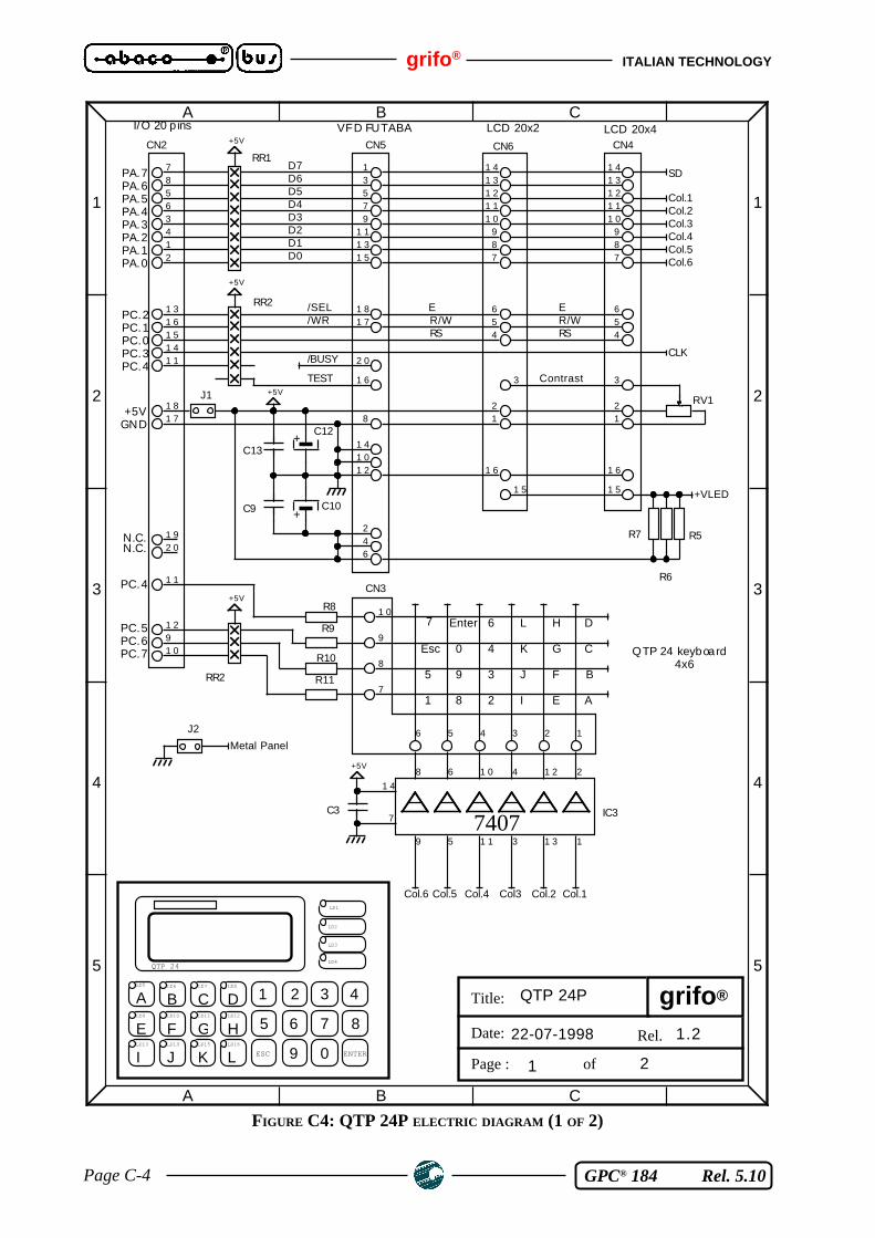
grifo ® ITALIAN TECHNOLOGY
Page C-4 GPC® 184 Rel. 5.10
FIGURE C4: QTP 24P ELECTRIC DIAGRAM (1 OF 2)
A
A
B
B
C
C
1 1
2 2
3 3
4 4
5 5
grifo ®Title:
Date:
Page : of
Rel.
1 2 3 4
5 6 7 8
9 0ESC ENTER
QTP 24
ALD5
BLD6
CLD7
DLD8
ELD9
FLD10
GLD11
HLD12
ILD13
JLD14
KLD15
LLD16
LD1
LD2
LD3
LD4
1.2
I/O 20 p ins VFD FUTABA
QTP 24 keyboard 4x6
L
K
J
AEI281
BF395
CG
H
40Esc
D6Enter7
LCD 20x4LCD 20x2
PA.7PA.6PA.5PA.4PA.3PA.2PA.1PA.0
PC.2PC.1PC.0PC.3PC.4
+5VGND
N.C.N.C.
PC.4
PC.5PC.6PC.7
QTP 24P
1 2
22-07-1998
7
CN2
8
RR1
563412
1
CN5
3579
1 11 31 5
1 4
CN6
1 31 21 11 0
987
1 31 61 5
1 1
1 81 7
1 1
1 29
1 4
1 0
1 8 654
654
2 0
1 6
1 41 0
4
821
1 6
3
21
1 51 5
3
C9
C13+
C12
R7
R6
R5
RV1
RR2
+C10
1 2
R8
R9
R10
R11
1 0
CN3
9
8
7
6 5 4 3 2 1
C3
+5V
+5V
+5V
+5V
1 92 0
+5V
7407
8 6 1 0 4 1 2 2
9 5 1 1 3 1 3 1
1 4
7 IC3
1 4
CN4
1 7
J1
6
2
RR2
J2
1 21 11 0
987
1 3
1 6
D6D7
/BUSY
EE
CLK
/WRRSRS
Contrast
+VLED
/SEL
TEST
D0
Col.6
Col.6
D1
Col.4
Col.4
Col.5
Col.5
D2D3
Col3
D4
Col.2
Col.2
D5
Col.1
Col.1
SD
R/W R/W
Metal Panel
Col.3

ITALIAN TECHNOLOGY grifo ®
Page C-5 GPC® 184 Rel. 5.10
FIGURE C5: QTP 24P ELECTRIC DIAGRAM (2 OF 2)
A
A
B
B
C
C
1 1
2 2
3 3
4 4
5 5
grifo ®Title:
Date:
Page : of
Rel.
22
1.2
QTP 24P
22-07-1998
LD1
LD2
LD3
LD4
LD5
LD16
LD15
LD14
LD13
LD12
LD11
LD10
LD9
LD8
LD7
LD6
D4 D3+5V
R3R4
R1
+5V
C2
+5V
C4
3
CN1
4
8÷24Vac
PD1
+ C8+ C7
+C11
+C5
+5V
16
15
1
13
14
12
11
10
9
8
7
6
5
4
3
2
28
27
26
25
2423222120191817
M 5 4 8 0
IC2SWITCHING
REGOLATOR
IC1
CLK
SD

grifo ® ITALIAN TECHNOLOGY
Page C-6 GPC® 184 Rel. 5.10
FIGURE C6: ABACO® I/O BUS INPUT OUTPUT ELECTRIC DIAGRAM
A
A
B
B
C
C
D
D
1 1
2 2
3 3
4 4
5 5
6 6
grifo ®Title:
Date:
Page : of
Rel.28/04/1999 1.2
ABACO® I/O BUS26 pin connector
Standard I/O20 pin connector
N.C.N.C.
+5V
GND
PA.7PA.6PA.5PA.4PA.3PA.2PA.1PA.0
PC.2PC.1PC.0
PC.3PC.4PC.5PC.6PC.7
Standard I/O20 pin connector
N.C.N.C.
+5V
GND
PA.7PA.6PA.5PA.4PA.3PA.2PA.1PA.0
PC.2PC.1PC.0
PC.3PC.4PC.5PC.6PC.7
A0A1A2
/RST
Power supply
Gnd
+5v
Dip Switch
Gnd
+Vcc
/CS2/CS1/NMI/INT
/IRQ
/RD/WR
D0D1D2D3D4D5D6D7
A3A4A5A6A7
I/O example
1 1
1
23
74HCT00
a
10K
10K
1N
41
48
2 1
+5V
1615141312
87654321
1718
19
23242122
20
26
2510
0nF
+22µF
+5V
D0D1D2D3D4D5D6D7
10K
+5V
+5V
+5V
10K
+5V
+22µF
100n
F
100n
F
100n
F
/G
P0P1P2P3P4P5P6P7
/P=Q
Q0Q1Q2Q3Q4Q5Q6Q7
1
2468
11131517
19
357912141618
74LS688
/G1/G2A1A2A3A4A5A6A7A8
Y1Y2Y3Y4Y5Y6Y7Y8
119
23456789
1817161514131211
74LS541
/GDIRA1A2A3A4A5A6A7A8
B1B2B3B4B5B6B7B8
191
23456789
1817161514131211
74LS245
9
108
74HCT00c
12
1311 74HCT00d
+5V
1
4
56
74HCT00
b
+5V
10K +5V
10K
+5V
+5V
10K 10K12345
11109
10K10K
A0A1A2
ABC
G1/G2A/G2B
Y0Y1Y2Y3Y4Y5Y6Y7
123
645
15141312111097
74LS138
A2A1A0
+5V
/CLRCLK
1D2D3D4D5D6D7D8D
1Q2Q3Q4Q5Q6Q7Q8Q
111
3478
13141718
256912151619
74LS273
+5V
D7D6D5D4D3D2D1D0
D7D6D5D4D3D2D1D0
1
23
74HCT32
a
9
108
74HCT32
c
12
1311
74HCT32
d
+5V
7
8563412
131615
1112
9
14
10
18
17
1920
100n
F+22µF
+5V
/CLRCLK
1D2D3D4D5D6D7D8D
1Q2Q3Q4Q5Q6Q7Q8Q
111
3478
13141718
256912151619
74LS273
+5V
D7D6D5D4D3D2D1D0
D7D6D5D4D3D2D1D0
1
23
74HCT32
a
7
8563412
131615
1112
9
14
10
18
17
1920
100n
F+22µF
+5V
10K
10K
10K
/G1/G2
A1A2A3A4A5A6A7A8
Y1Y2Y3Y4Y5Y6Y7Y8
119
23456789
1817161514131211
74LS541
/G1/G2
A1A2A3A4A5A6A7A8
Y1Y2Y3Y4Y5Y6Y7Y8
119
23456789
1817161514131211
74LS541
N.C.N.C.N.C.N.C.
RES
/RST
/RST
BA3
BA5
BA7BA6
BA4
/BIRQ
BD0
BD2
BD7BD6BD5BD4BD3
BD1
/BWR/BRD/BRSTBA2
BA0BA1
/CS
/CS
/CS
/CS3/CS4/CS5/CS6/CS7/CS8
/RES
/RES
/RES
/RES
/RD
/RD
/RD
/CS2
/CS2
/CS2
/CS1
/CS1
/CS1
/WR
/WR
/WR
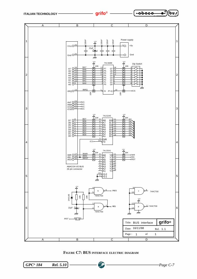
ITALIAN TECHNOLOGY grifo ®
Page C-7 GPC® 184 Rel. 5.10
FIGURE C7: BUS INTERFACE ELECTRIC DIAGRAM
A
A
B
B
C
C
D
D
1 1
2 2
3 3
4 4
5 5
6 6
grifo ®Title:
Date:
Page : of
Rel.16/11/98
ABACO® I/O BUS26 pin connector
/RST
A0A1
Power supply
Gnd
+5v
Dip Switch
Gnd
+Vcc
/CS2/CS1/NMI/INT
/IRQ
/RD/WR
D0D1D2D3D4D5D6D7
A2A3A4A5A6A7
1.1
BUS interface
1 1
1
23
74HCT00
a
10K
10K
1N
41
48
2 1
+5V
161514131211
87654321
1718
19
23242122
20
26
25
100n
F
+22µF
+5V
D0D1D2D3D4D5D6D7
10K
+5V
+5V
+5V
10K
+22µF
100n
F
100n
F
100n
F
/G
P0P1P2P3P4P5P6P7
/P=Q
Q0Q1Q2Q3Q4Q5Q6Q7
1
2468
11131517
19
357912141618
74LS688
/G1/G2A1A2A3A4A5A6A7A8
Y1Y2Y3Y4Y5Y6Y7Y8
119
23456789
1817161514131211
74LS541
/GDIRA1A2A3A4A5A6A7A8
B1B2B3B4B5B6B7B8
191
23456789
1817161514131211
74LS245
9
108
74HCT00c
12
1311 74HCT00d
+5V
1
4
56
74HCT00
b
+5V
10K
10K
+5V
+5V
10K10K12345678
109
10K10K
N.C.N.C.N.C.N.C.
/RD/WR
/CS
/CS
RES
/RES
/RST
/RST
BA2BA3
BA5
BA7BA6
BA4
/BIRQ
BD0
BD2
BD7BD6BD5BD4BD3
BD1
/BWR/BRD/BRST
BA0BA1

grifo ® ITALIAN TECHNOLOGY
Page C-8 GPC® 184 Rel. 5.10
FIGURE C8: IAC 01 ELECTRIC DIAGRAM
A
A
B
B
C
C
D
D
1 1
2 2
3 3
4 4
5 5
grifo ®Title:
Date:
Page : of
Rel.
D2D3D4D5D6D7D8/ACKBUSYPESELECT/AUTOLF
/STROBED1
/FAULT/RESETMODE
13-11-98 1.1
IAC 01
1 1
1521436587121011916201314191817
CN220 pin Low-Profile Male
123456789
10111213141516171819202122232425
CN1
25 pin D-Type Female
C11
2,2 nF
C10 2,2 nF
C9
2,2 nF
C8 2,2 nF
C7
2,2 nF
C6 2,2 nF
C5
2,2 nF
C4 2,2 nF
C3
2,2 nF
C2
100 nF
+
C1
22 µF 6,3V
RR14,7 KΩ 9+1
+5V
P1.4
P1.5
P1.6
P1.7
P0.7P0.6P0.5P0.4P0.3P0.2
P0.0P0.1
P1.3P1.2
P1.1
P1.0
+5VGND

ITALIAN TECHNOLOGY grifo ®
Page D-1 GPC® 184 Rel. 5.10
APPENDICE D: ALPHABETICAL INDEXAPPENDICE D: ALPHABETICAL INDEX
Simbols
/CS1 3582c55 43, C-1
A
ABACO ® I/O BUS 6, 7, 10, 27, 35, 42, C-5Addresses 35
ABACO® I/O BUS 35I/O 37memory 36
Assistance 1
B
Back up 8, 9, 26Battery 8, 9, 24, 26Baud rate 20Bibliography 44Block diagram 5
C
Clock 4, 7Components maps11Configuration jumper 4, 7, 24, 27, 38, 41Connections diagram43Connectors 7, 9, 15
CN1 10, 35CN2 9CN3A 12CN3B 14, 30CN5 19, 20
Consumption 8Container 1, 7, A-1Control logic 6CPU 3, 7, B-1CPU devices 27, 38, 41, B-1Crystal 4, 7Current loop 4, 7, 14, 18, 21, 28
D
DEBUG 4, 27, 41Default configuration 22, 26, 28Devices 7Dimension A-1

grifo ® ITALIAN TECHNOLOGY
Page D-2 GPC® 184 Rel. 5.10
DIN Ω rails 7, A-1DMA 7
E
Electric diagram C-1EPROM 3, 7, 26, 36Expansion 6, 42, C-1External cards 42
F
Featureselectric 8general 2, 7physical 7technical 7
FLASH EPROM 3, 7, 26, 36
H
Handshake 12, 24, 30Humidity 7
I
I/O addresses 37I/O connection 21I/O lines C-1Installation 9Interfaces C-1Interrupt 10, 20, 27, 31, 40
J
Jumpers 222 pins 243 pins 255 pins 25
Jumpers location 23
L
LED 15, 21
M
Maintenance 1Maps 35Memory 3, 7, 15, 25, 26, 36MMU 36

ITALIAN TECHNOLOGY grifo ®
Page D-3 GPC® 184 Rel. 5.10
Mounting A-1
N
Network 17
O
On board devices 35Operator interface 42, C-3, C-4Options 26, 28, 30, A-1
P
Peripheral devices39Photo 11Piggy back 45Power failure 7, 8, 10, 25, 27, 31Power supply 4, 8, 10, 31Printer C-8
R
RAM 3, 7, 26, 36Real Time Clock 6, 7, 21, 27, 38, 39Registers 38Release 1Reset 31Reset contact 6, 7RS 232 4, 7, 12, 14, 16, 21, 28RS 422 4, 7, 8, 14, 16, 21, 24, 28RS 485 4, 7, 8, 14, 16, 17, 21, 24, 30RUN 4, 27, 41
S
Serial communication 13Serial drivers 29Serial line A 12, 30Serial line B 14, 28Serial lines 4, 7, 12, 14, 28Size 7Software 32Solder jumpers 27Synchronous serial20
T
Temperature 7Termination circuit 8, 30

grifo ® ITALIAN TECHNOLOGY
Page D-4 GPC® 184 Rel. 5.10
Timers 7TransZorb™ 4TTL 21
V
Version 1
W
Warranty 1Watch dog 6, 7, 24, 30, 38, 41Weight 7