Controlling the Flow: Next‐Generation Power Electronics ... Project... · GaN Initiative for Grid...
25
Controlling the Flow: Next‐Generation Power Electronics Systems for Tomorrow’s Electric Grid GaN Initiative for Grid Applications (GIGA) Project Summary Prepared for the U.S. Department of Energy, Office of Electricity Delivery and Energy Reliability by Energetics Incorporated in collaboration with Kerry Cheung. December 2015
Transcript of Controlling the Flow: Next‐Generation Power Electronics ... Project... · GaN Initiative for Grid...
ControllingtheFlow:Next‐GenerationPowerElectronicsSystemsforTomorrow’sElectricGridGaNInitiativeforGridApplications(GIGA)ProjectSummary
Prepared for the U.S. Department of Energy, Office of Electricity Delivery and Energy Reliability
by Energetics Incorporated in collaboration with Kerry Cheung.
December 2015
GaN INITIATIVE FOR GRID APPLICATIONS (GIGA) PROJECT SUMMARY
2
ExecutiveSummary
IntroductionThe development of next‐generation power electronics (PE) systems is critical to enhance the capabilities
of today’s aging electric grid to adequately control, absorb, and reroute power. These advanced PE
systems include solid‐state transformers, inverters, fault current limiters, high‐voltage direct current, and
power flow controllers. Existing PE systems play a key role in our electricity delivery system, enabling
electric power conversion (e.g., AC to DC, DC to AC, or DC to
DC) and improved power transmission and distribution (T&D).
These systems can help reduce transmission and distribution
losses, optimize power delivery, protect critical assets, and
enhance grid resilience.1For example, over the last decade,
congestion charges ranged from $1 to $2B annually at PJM, one
of the largest regional transmission organizations.2 Additionally, weather‐related outages are estimated
to cost the U.S. $25 to $70B annually (outages from Superstorm Sandy was estimated to cost $52B).3 Grid
enhancements through the use of next‐generation PE systems can lead to significant savings among other
benefits. Despite these advantages, large‐scale deployment of advanced PE systems remains limited
because of high costs, inadequate performance levels, and insufficient technological maturity.
Providing the core functionality of these systems are PE devices such as transistors, diodes, and thyristors
that can comprise up to 50% of the installed costs.4 The essential material needed to fabricate these PE
devices are semiconductors that have traditionally been silicon, the bedrock material of the computer
integrated circuit industry. However, advanced PE devices are now being fabricated using wide bandgap
(WBG) semiconductor materials such as silicon carbide (SiC) and gallium nitride (GaN). These WBG
semiconductors possess superior material properties that enable device operation at higher temperatures
and voltages with faster switching speeds—resulting in smaller, more reliable, and more efficient PE
systems with higher levels of control, flexibility, and performance.
While each of these three materials—silicon, SiC, and GaN—have the potential to help modernize the
aging electric grid, the U.S. Department of Energy (DOE) Office of
Electricity Delivery and Energy Reliability (OE) GaN Initiative for
Grid Applications (GIGA) project focused on the development of PE
devices based on gallium nitride on silicon (GaN‐on‐Si) technology.
GaN‐on‐Si technology effectively combines the enhanced material
properties of GaN with the well‐established, low‐cost, and high‐
1 U.S. Energy Information Administration (EIA). “Frequently Asked Questions.” Last updated July 10, 2015. Accessed November 29, 2015. 2 Market Monitoring Analytics, LLC. “2012 Quarterly State of the Market Report for PJM: January through March”. 3 Congressional Research Service. “Weather‐Related Power Outages and Electric System Resiliency” Aug 28, 2012. 4 Power Electronics for Distributed Energy Systems and Transmission and Distribution Applications, Oak Ridge National Laboratory, 2005.
Approximately 6% of U.S. electricity generated annually is lost in transmission and distribution (T&D) due to inefficiencies. This is the equivalent of powering the state of California for one year.1
GaN‐on‐Si PE devices are a disruptive technology that offers unique opportunities to cost‐effectively integrate enhanced control capabilities into the grid.
GaN INITIATIVE FOR GRID APPLICATIONS (GIGA) PROJECT SUMMARY
3
volume manufacturability of silicon.5 By fabricating PE devices using GaN‐on‐Si technology to support the
development of next‐generation PE systems, WBG material performance at silicon prices is possible for a
broad range of grid applications. The potential affordability and fundamental cost advantages of utilizing
GaN‐on‐Si PE devices is a critical benefit over other WBG technologies. In addition, because GaN‐on‐Si PE
devices are built on silicon wafers, this material option gives greater flexibility for integration with silicon
based technologies, including control electronics for enhanced functionality.
GIGAProjectImpactsThe GIGA project was initiated in late 2009 at a time when GaN‐on‐Si development efforts in the United
States were still in their infancy for PE applications. Many in the industry considered it technically
challenging and impractical for GaN‐on‐Si PE devices to operate at
voltages over 600 V. The GIGA project worked to overcome this
challenge. Overall, the project produced a number of important
advances and valuable insights in the development of GaN‐on‐Si
PE devices and provided critical proofs‐of‐concept to demonstrate
what is possible with GaN‐on‐Si technology. Today, the power
electronics industry, including many non‐U.S. companies,6 is investigating GaN‐on‐Si PE devices at
voltages greater than 1200 V alongside production of various other GaN‐on‐Si devices at lower voltages.
The GIGA project helped to catalyze and develop an industrial base for high powered GaN‐on‐Si PE devices
that can be utilized across multiple sectors of the U.S. economy.
GIGA results have helped pique industry interest, spurring competition and investment. The GIGA project
supported the maturation of the U.S. GaN‐on‐Si industry through its effective use of public‐private
collaborations to achieve significant technical milestones and proofs‐of‐concept. Achievements were
supported and disseminated to the public through more than 75 GIGA‐related publications in various
technical journals and magazines. These milestones include:
Materials Advancement: Catalyzed a low‐cost domestic supply of high‐quality 200 mm GaN‐on‐
Si wafers, critical to realizing the affordability of GaN‐on‐Si PE devices.
Device Development: Demonstrated GaN‐on‐Si is a viable technology for high power applications
(> 1.2 kV) and developed world record GaN‐on‐Si diodes and transistors (> 3 kV and > 15 A).
Enhanced Manufacturability: Demonstrated prototype manufacturing process runs that are
compatible with high‐volume, low‐cost, integrated circuit production facilities.
MoreWorkisNeededWhile the GIGA project successfully demonstrated that GaN‐on‐Si technology is viable as a basis for
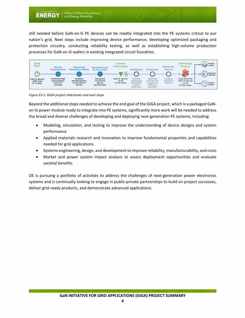
manufacturing cost‐effective high power PE devices, Figure ES‐1 highlights some of the additional work
5 Over 180 million eight inch silicon wafers were consumed in 2013 according to SEMI, the global semiconductor industry association. By comparison, less than 900,000 eight inch equivalent SiC wafers were consumed for power in 2013 according to Yole Research. 6 Compound Semiconductor magazine, Commercial status of the GaN‐on‐silicon power industry, March 2013. www.compoundsemiconductor.net. http://www.compoundsemiconductor.net/pdf/magazines/2013/cs‐2013‐volume‐19‐issue‐2.pdf.
The GIGA project has helped to create a domestic GaN‐on‐Si industry and built the foundation to dramatically reduce the cost of key building blocks of next‐generation grid components.
GaN INITIATIVE FOR GRID APPLICATIONS (GIGA) PROJECT SUMMARY
4
still needed before GaN‐on‐Si PE devices can be readily integrated into the PE systems critical to our
nation’s grid. Next steps include improving device performance, developing optimized packaging and
protection circuitry, conducting reliability testing, as well as establishing high‐volume production
processes for GaN‐on‐Si wafers in existing integrated circuit foundries.
Figure ES‐1: GIGA project milestones and next steps
Beyond the additional steps needed to achieve the end goal of the GIGA project, which is a packaged GaN‐
on‐Si power module ready to integrate into PE systems, significantly more work will be needed to address
the broad and diverse challenges of developing and deploying next‐generation PE systems, including:
Modeling, simulation, and testing to improve the understanding of device designs and system
performance
Applied materials research and innovation to improve fundamental properties and capabilities
needed for grid applications
Systems engineering, design, and development to improve reliability, manufacturability, and costs
Market and power system impact analysis to assess deployment opportunities and evaluate
societal benefits
OE is pursuing a portfolio of activities to address the challenges of next‐generation power electronics
systems and is continually looking to engage in public‐private partnerships to build on project successes,
deliver grid‐ready products, and demonstrate advanced applications.
GaN INITIATIVE FOR GRID APPLICATIONS (GIGA) PROJECT SUMMARY
5
I. PowerElectronicsSystemsfortheGrid
Greaterdeploymentofpowerelectronicssystemsiscriticaltorealizingthefutureelectricgrid.
For more than a century, the nation’s electric grid has powered our economy, sustained our industrial and
individual needs, and raised our quality of life. However, the electric grid is being challenged to address
the requirements of our digitalizing economy, more decentralized generation and controls, and
accelerated progress towards an environmentally responsible future. These profound changes affecting
the electric power sector offer an unprecedented opportunity to transform the grid. Increasing needs for
flexibility, reliability, and resilience in the transmission and distribution (T&D) system require technologies
and techniques not conceived of when much of the current infrastructure was deployed. During this
period of transition, the deployment of new technologies will play a critical role in shaping the future grid.
Next‐generation power electronics (PE) systems are one of the key solutions to modernize the electric
grid among other technological improvements needed. These advanced technologies—including solid‐
state transformers, fault current limiters, high‐voltage direct current, and power flow controllers—can
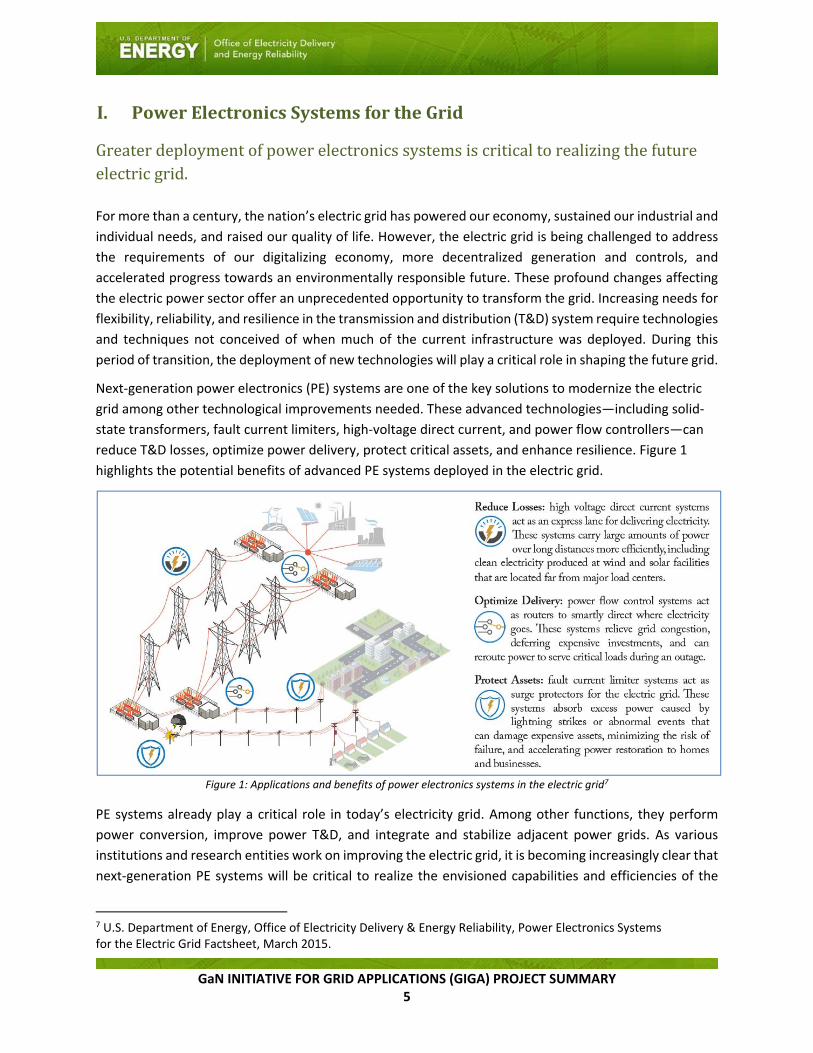
reduce T&D losses, optimize power delivery, protect critical assets, and enhance resilience. Figure 1
highlights the potential benefits of advanced PE systems deployed in the electric grid.
Figure 1: Applications and benefits of power electronics systems in the electric grid7
PE systems already play a critical role in today’s electricity grid. Among other functions, they perform
power conversion, improve power T&D, and integrate and stabilize adjacent power grids. As various
institutions and research entities work on improving the electric grid, it is becoming increasingly clear that
next‐generation PE systems will be critical to realize the envisioned capabilities and efficiencies of the
7 U.S. Department of Energy, Office of Electricity Delivery & Energy Reliability, Power Electronics Systems for the Electric Grid Factsheet, March 2015.
GaN INITIATIVE FOR GRID APPLICATIONS (GIGA) PROJECT SUMMARY
6
future grid. Greater deployment of next‐generation PE systems can more effectively handle the projected
changes in the electric grid, diminish losses during power conversions, and reduce the need for auxiliary
components.
Widebandgap(WBG)PEdevicescanenhancePEsystems.Despite the advantages offered by PE systems, large‐scale deployment of these systems remains limited
because of high costs, inadequate performance levels, and insufficient technological maturity. In today’s
systems, silicon PE devices (such as transistors, diodes, and thyristors) are the most widely used
technology. However, silicon‐based PE systems will be increasingly challenged to cost‐effectively meet
the new capabilities and growing performance demands of future grid applications. Next‐generation PE
systems based on advanced materials, such as wide bandgap (WBG) semiconductors (e.g., silicon carbide
(SiC), gallium nitride (GaN)), allow for new designs and capabilities that can dramatically shift the cost‐
performance curves. While silicon PE devices are rapidly approaching their maximum performance limits
for high power applications, advances in WBG PE devices show the potential for operation at higher
voltages, higher temperatures, and higher frequencies by virtue of their material properties (see Table 1
below). The limitations of silicon PE devices directly impact the performance and cost of grid PE systems
that utilize them including:
Voltage Limits: Grid applications typically require systems that can operate at tens to hundreds
of thousand volts. This requirement means that multiple silicon‐based devices are typically
connected together in series or “stacked” to achieve the desired voltage rating. Stacked structures
are more expensive (proportional to the number stacked) and often require complicated
triggering and control circuitry to maintain voltage‐sharing between devices in the stack.8
Temperature Limits: Grid applications typically involve the control of hundreds to thousands of
amps of electrical current, leading to high temperatures due to resistive heating. Silicon‐based
devices must be operated below 150°C to preserve functionality and integrated cooling systems
are often used to meet this requirement. These systems of pumps, radiators, and fans adds to
total system costs, increases volume and weight, and increases maintenance costs.
Frequency Limits: The size of supporting PE circuit elements, such as capacitors and inductors,
and PE system components, such as transformers, are directly related to the device operating
frequency. Silicon‐based devices typically do not operate at frequencies greater than 5 kHz in grid
applications, resulting in large PE modules and system components with greater associated costs
for materials.
8 L.M. Tolbert, B. Ozpineci, S.K. Islam, and M.S. Chinthavalli “Wide Bandgap Semiconductors for Utility Applications” Proceeding (379) Power and Energy Systems ‐ 2003 http://power.eecs.utk.edu/pubs/iasted_2003_wide_bandgap.pdf.
GaN INITIATIVE FOR GRID APPLICATIONS (GIGA) PROJECT SUMMARY
7
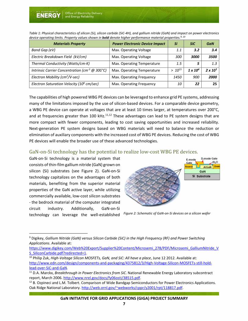
Table 1: Physical characteristics of silicon (Si), silicon carbide (SiC‐4H), and gallium nitride (GaN) and impact on power electronics device operating limits. Property values shown in bold denote higher performance material properties.9, 10
Materials Property Power Electronic Device Impact Si SiC GaN
Band Gap (eV) Max. Operating Voltage 1.1 3.2 3.4
Electric Breakdown Field (kV/cm) Max. Operating Voltage 300 3000 3500
Thermal Conductivity (Watts/cm‐K) Max. Operating Temperature 1.5 5 1.3
Intrinsic Carrier Concentration (cm‐3 @ 300°C) Max. Operating Temperature > 1015 1 x 10⁴ 2 x 10²
Electron Mobility (cm2/V‐sec) Max. Operating Frequency 1450 900 2000
Electron Saturation Velocity (106 cm/sec) Max. Operating Frequency 10 22 25
The capabilities of high powered WBG PE devices can be leveraged to enhance grid PE systems, addressing
many of the limitations imposed by the use of silicon‐based devices. For a comparable device geometry,
a WBG PE device can operate at voltages that are at least 10 times larger, at temperatures over 200°C,
and at frequencies greater than 100 kHz.11,12 These advantages can lead to PE system designs that are
more compact with fewer components, leading to cost saving opportunities and increased reliability.
Next‐generation PE system designs based on WBG materials will need to balance the reduction or
elimination of auxiliary components with the increased cost of WBG PE devices. Reducing the cost of WBG
PE devices will enable the broader use of these advanced technologies.
GaN‐on‐Sitechnologyhasthepotentialtorealizelow‐costWBGPEdevices.GaN‐on‐Si technology is a material system that
consists of thin‐film gallium nitride (GaN) grown on
silicon (Si) substrates (see Figure 2). GaN‐on‐Si
technology capitalizes on the advantages of both
materials, benefiting from the superior material
properties of the GaN active layer, while utilizing
commercially available, low‐cost silicon substrates
‐ the bedrock material of the computer integrated
circuit industry. Additionally, GaN‐on‐Si
technology can leverage the well‐established
9 Digikey, Gallium Nitride (GaN) versus Silicon Carbide (SiC) in the High Frequency (RF) and Power Switching Applications. Available at: https://www.digikey.com/Web%20Export/Supplier%20Content/Microsemi_278/PDF/Microsemi_GalliumNitride_VS_SiliconCarbide.pdf?redirected=1. 10 Philip Zuk, High‐Voltage Silicon MOSFETs, GaN, and SiC: All have a place, June 12 2012. Available at: http://www.edn.com/design/components‐and‐packaging/4375812/3/High‐Voltage‐Silicon‐MOSFETs‐still‐hold‐lead‐over‐SiC‐and‐GaN. 11 D.A. Marckx, Breakthrough in Power Electronics from SiC. National Renewable Energy Laboratory subcontract report, March 2006. http://www.nrel.gov/docs/fy06osti/38515.pdf. 12 B. Ozpineci and L.M. Tolbert. Comparison of Wide Bandgap Semiconductors for Power Electronics Applications. Oak Ridge National Laboratory. http://web.ornl.gov/~webworks/cppr/y2001/rpt/118817.pdf.
Figure 2: Schematic of GaN‐on‐Si devices on a silicon wafer
GaN INITIATIVE FOR GRID APPLICATIONS (GIGA) PROJECT SUMMARY
8
integrated circuit processing facilities for low‐cost PE device production. In short, GaN‐on‐Si technology
enables WBG material performance at silicon prices for a broad range of power applications.
The potential affordability and fundamental cost structure advantage of GaN‐on‐Si lateral PE devices
(where current flows across the surface of the wafer) is a critical advantage over other WBG technologies.
While GaN can be grown on various substrates (e.g., Si, SiC, GaN, sapphire) with modest incremental costs,
the cost of these material systems are dominated by the substrate. The production of Si substrates is
much less expensive and consumes less energy than SiC substrates, as the latter is grown at much higher
temperatures and much slower rates (~1‐2 mm/hr for SiC vs. 100 mm/hr for Si).13,14,15,16 Currently, there
are no suppliers of large diameter GaN substrates and sapphire substrates remains very expensive.
Vertical PE devices (where current flows through the wafer) have the capability for inherently higher
power densities than lateral devices, but face affordability issues due to the high cost of WBG substrates.
II. GIGAProjectOverviewThe U.S. Department of Energy (DOE) Office of Electricity Delivery and Energy Reliability (OE) GaN Initiative
for Grid Applications (GIGA) project focused on the development of
high power PE devices based on GaN‐on‐Si technology. A basic
driver for GIGA is that WBG PE devices should be closer in cost
structure to conventional silicon‐based alternatives in order to
enable broad deployment. GIGA led the way in the development of
lateral PE devices on a material system with significant cost advantages for grid PE systems application.
While SiC is currently at a more advanced stage compared to GaN‐on‐Si for the development of high
power PE devices, this came about after more than a decade of Department of Defense investments.
Several DOE programs initiated after GIGA continue to address cost challenges associated with WBG PE
devices (e.g., Power America, SWITCHES).17
GaN‐on‐Si lateral devices take advantage of the very high electron mobility at the AlGaN/GaN interface
(~2000 cm2/V‐sec) leading to lower conduction losses and higher efficiencies. Additionally, lateral devices
make the fabrication process much easier and more cost‐effective than vertical devices. While there has
been significant commercial interest in developing GaN‐on‐Si PE devices for low voltage (< 1 kV)
applications, limited attention was given to higher voltages. Many in the industry considered it technically
challenging and impractical for GaN‐on‐Si PE devices to operate at voltages over 600 V when GIGA started.
The GIGA project focused on developing materials and devices capable of operating at voltages > 1 kV.
Since GaN‐on‐Si PE devices are built on silicon substrates, integration with silicon‐based technologies such
13 Carl‐Mikael Zetterling, Process Technology for Silicon Carbide Devices, 2002. 14 Wai‐Kai Chen, The VLSI Handbook, Chapter 5: Silicon Carbide Technology, 2007. 15 S. E. Saddow and A. Agarwal. Advances in Silicon Carbide Processing and Applications. 2004. 16 Tsunenobu Kimoto and James A. Cooper. Fundamentals of Silicon Carbide Technology: Growth, Characterization, Devices and Applications. 2014. 17 ARPA‐E SWITCHES Program: http://arpa‐e.energy.gov/?q=arpa‐e‐programs/switches.
More than 75 GIGA related publications provided industry and other stakeholders with the results of GaN‐on‐Si studies
GaN INITIATIVE FOR GRID APPLICATIONS (GIGA) PROJECT SUMMARY
9
as control electronics is readily possible. New hybrid circuits optimized for high voltage applications can
lead to enhanced capabilities at reduced costs.18
Silicon‐based PE devices with low to midrange power ratings are widely utilized at high production
volumes in the consumer and transportation sectors. However, high power versions for the utility sector
lack the production volumes needed to help drive down costs.19 As commercial WBG PE devices gain
market share in industry segments such as electric vehicles, solar PV inverters,20 lighting, and consumer
electronics, cost challenges from production volumes will persist for high power versions. As illustrated in
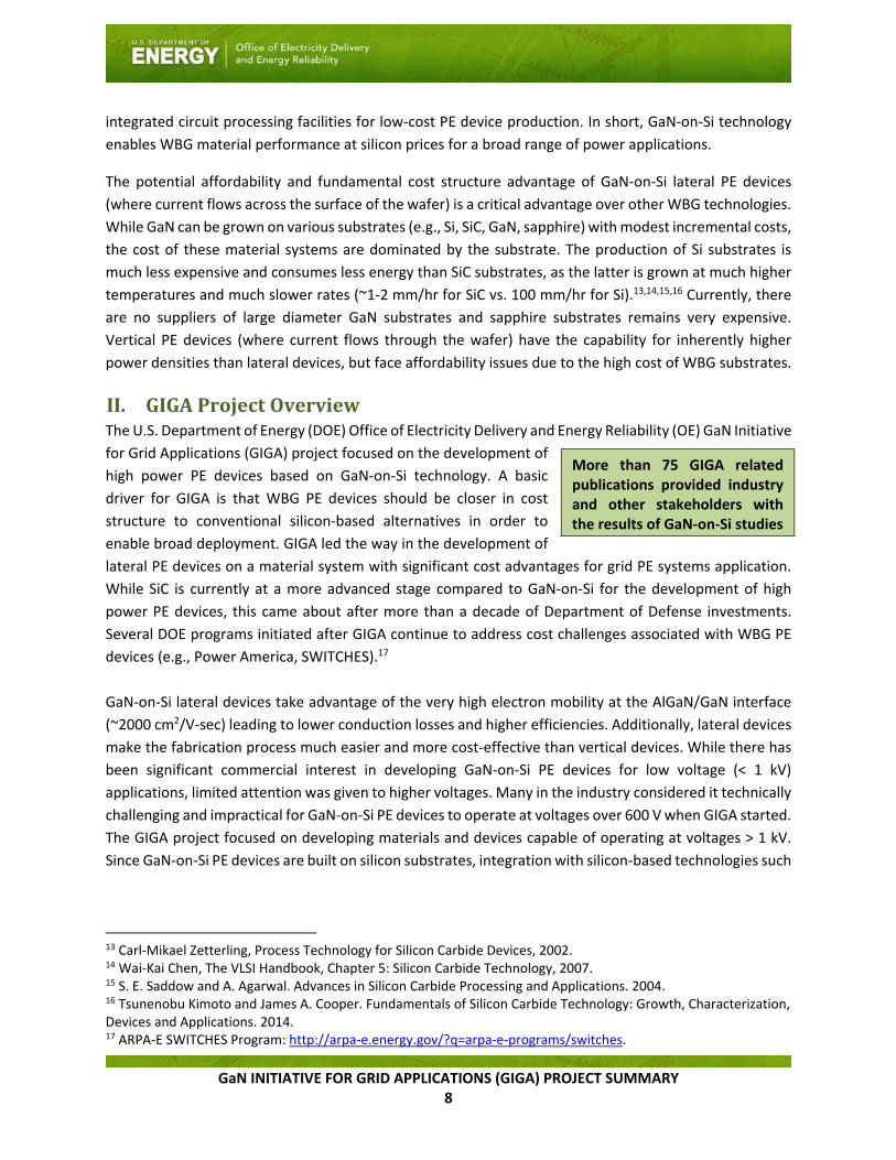
Figure 3, the technology developed through GIGA would alter this paradigm. High power GaN‐on‐Si PE
devices that leverage the manufacturing processes and cost advantages of low power products (i.e., high
volumes) can be used in the utility sector with new designs for grid PE systems.
Figure 3: Power electronics devices span across many applications with different power ratings and production volumes. Utility
applications can benefit from high power devices that leverage high volume manufacturing.
The GIGA team began work in October 2009 to advance GaN‐on‐Si materials and device technology for
cost‐effective, WBG PE devices suitable for grid PE systems application. The initial team, formed via
competitive R&D research subcontracts in August 2009, was led by MIT Lincoln Laboratory (MIT/LL) and
included the MIT campus Advanced Semiconductor Materials and Devices research group (MIT) and
MACOM Technology Solutions (MTS). Oak Ridge National Laboratory and Sandia National Laboratories
were also part of the team, providing key advanced packaging reliability testing and device reliability
testing, respectively. By December 2012, the fourth core member, IQE (Kopin Corp. at the time21), joined
18 Jinwook W. Chung, “Millimeter‐wave GaN high electron mobility transistors and their integration with silicon electronics,” MIT (2011), http://dspace.mit.edu/handle/1721.1/63065#files‐area. 19 B. Ozpineci, M.S. Chintavali, and L. M. Tolbert, Enhancing Power Electronic Devices with Wide Bandgap Semiconductors, (Oak Ridge, TN: Oak Ridge National Laboratory, 2007). 20 H. Zhang, L. Tolbert, B. Ozpineci, “Impact of SiC devices on Hybrid Electric and Plug‐in Hybrid Electric Vehicles,” Industry Applications Society Annual Meeting, October 2008, pp. 1‐5. 21 IQE acquired Kopin Wireless in January 2013.
GaN INITIATIVE FOR GRID APPLICATIONS (GIGA) PROJECT SUMMARY
10
the team to provide a domestic supply of commercial‐grade GaN epitaxial materials. The project period
of performance ended in September 2014.
Overall, the project produced a number of important advances and valuable insights in the development
of GaN‐on‐Si PE devices and provided critical proofs‐of‐concept to demonstrate what is possible with GaN‐
on‐Si technology. Today, the power electronics industry, including many non‐U.S. companies,22 is
investigating GaN‐on‐Si PE devices at voltages greater than 1200 V alongside production of various other
GaN‐on‐Si devices at lower voltages. The GIGA project helped to catalyze and develop an industrial base
for high powered GaN‐on‐Si PE devices that can be utilized across multiple sectors of the U.S. economy.
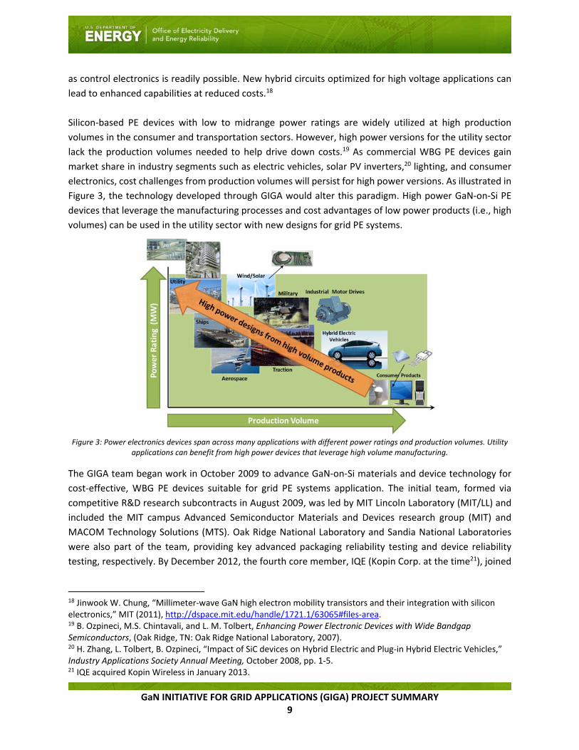
A key factor in enabling the advancements made throughout the GIGA project was the integrated team
approach that brought together device experts, materials experts, and companies with the ability to
commercialize and manufacture devices. This well‐structured team included distinct, complementary
roles for each performer, as illustrated in Figure 4.
Figure 4: The GIGA Team: MIT Lincoln Laboratory, MIT, MACOM, and IQE, ORNL and SNL.
III. ProjectAccomplishmentsandTechnicalAdvancesAn important contribution of the GIGA project was analyzing the performance trade‐offs between lateral
and vertical GaN‐based power transistors.23 The conventional wisdom from traditional silicon device
development is that thermal dissipation issues would render lateral devices inappropriate at high power.
GIGA results and simulations suggest that under certain scaling conditions (up to 5 kV), lateral GaN‐on‐Si
power transistors have similar thermal performance as vertical GaN power transistors. Since vertical
devices are much more expensive to fabricate, GaN‐on‐Si devices would be the preferable option. While
vertical devices have the capability for inherently higher power densities than lateral devices, this PE
device attribute is not as critical for grid PE systems application which is much more sensitive to costs.
22 Compound Semiconductor magazine, Commercial status of the GaN‐on‐silicon power industry, March 2013. www.compoundsemiconductor.net. Available at: http://www.compoundsemiconductor.net/pdf/magazines/2013/cs‐2013‐volume‐19‐issue‐2.pdf. 23 Yuhao Zhang, “Simulation and Fabrication of GaN‐Based Vertical and Lateral Normally‐off Power Transistors”, 2013. Available at: http://dspace.mit.edu/bitstream/handle/1721.1/82179/861974857‐MIT.pdf?sequence=2.
Materials & advanced
packaging reliability testing
Device reliability testing Team lead: Materials growth
and device technology
Device design and
processing
Commercial epitaxial
material supplier
Commercial device foundry
– advanced device
GaN INITIATIVE FOR GRID APPLICATIONS (GIGA) PROJECT SUMMARY
11
The GIGA project advanced the performance landscape of GaN‐on‐Si PE devices, addressing concerns
within the research community of the viability of lateral devices at high power levels. While GIGA focused
on power applications, project results has helped advance other applications and sectors. For example,
the advances in material and device processing also support radio frequency (RF) applications. Full details
of these accomplishments and technical advances are available in the GIGA Final Technical Report and
include:
Materials Advancement: Catalyzed a low‐cost domestic supply of high‐quality 200 mm GaN‐on‐
Si wafers, critical to realizing the affordability of GaN‐on‐Si PE devices.
Device Development: Demonstrated GaN‐on‐Si is a viable technology for high power applications
(>1.2 kV) and developed world record GaN‐on‐Si diodes and transistors (>3 kV and >15 A).
Enhanced Manufacturability: Demonstrated prototype manufacturing process runs that are
compatible with high‐volume, low‐cost, integrated circuit production facilities.
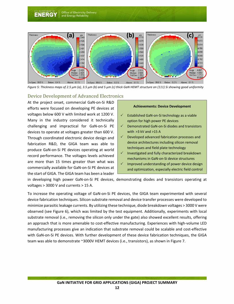
MaterialsAdvancementforHighQualityWafersAt the project onset, the domestic production of GaN‐
on‐Si wafers were not of sufficient quality to support
development of high power GaN‐on‐Si PE devices. The
GIGA team had to rely on a high‐priced Japanese
supplier, limiting the affordability of GaN‐on‐Si PE
devices. To address this foundational challenge, the
GIGA team developed techniques to produce low cost
wafer materials. R&D efforts advanced progress from
exploratory material growth techniques in a laboratory
setting to the point where high quality GaN‐on‐Si
wafers could be produced at 8‐inch (200 mm) silicon wafer manufacturing facilities. Due in part to GIGA
achievements, there are now at least three companies that have been able to develop commercial GaN‐
on‐Si epitaxial capabilities. The result is a robust domestic supply of affordable, high‐quality commercial
GaN‐on‐Si wafers that did not exist before.
The GIGA project also made multiple material growth and characterization advances. One major technical
challenge was the post‐growth wafer bow due to stress between the materials needed to form the GaN
High Electron Mobility Transistor (HEMT) structure and the silicon substrate. Managing the buildup of
stress in the epitaxial growth process becomes more challenging as the GaN HEMT structure becomes
thicker which is required for high voltage devices. The GIGA team developed in‐situ monitoring techniques
and improved growth processes to address this challenge. By the end of the project, the GIGA team
demonstrated the growth of 5 µm thick GaN HEMT structures that were crack‐free with good uniformity
(see Figure 5). These GaN‐on‐Si wafers showed < 50 µm wafer bow, which is virtually flat and necessary
for PE device fabrication.
Achievements: Materials Advancement
Catalyzed the development of domestic
commercial suppliers of GaN‐on‐Si wafers
with sizes from 100 mm to 200 mm
Improved understanding of epitaxial
materials growth and characterization
Demonstrated the growth of a virtually flat,
crack‐free GaN HEMT structure on Si
substrate up to 5 µm in thickness
GaN INITIATIVE FOR GRID APPLICATIONS (GIGA) PROJECT SUMMARY
12
Figure 5: Thickness maps of 2.5 µm (a), 3.5 µm (b) and 5 µm (c) thick GaN HEMT structure on (111) Si showing good uniformity
DeviceDevelopmentofAdvancedElectronicsAt the project onset, commercial GaN‐on‐Si R&D
efforts were focused on developing PE devices at
voltages below 600 V with limited work at 1200 V.
Many in the industry considered it technically
challenging and impractical for GaN‐on‐Si PE
devices to operate at voltages greater than 600 V.
Through coordinated electronic device design and
fabrication R&D, the GIGA team was able to
produce GaN‐on‐Si PE devices operating at world
record performance. The voltages levels achieved
are more than 15 times greater than what was
commercially available for GaN‐on‐Si PE devices at
the start of GIGA. The GIGA team has been a leader
in developing high power GaN‐on‐Si PE devices, demonstrating diodes and transistors operating at
voltages > 3000 V and currents > 15 A.
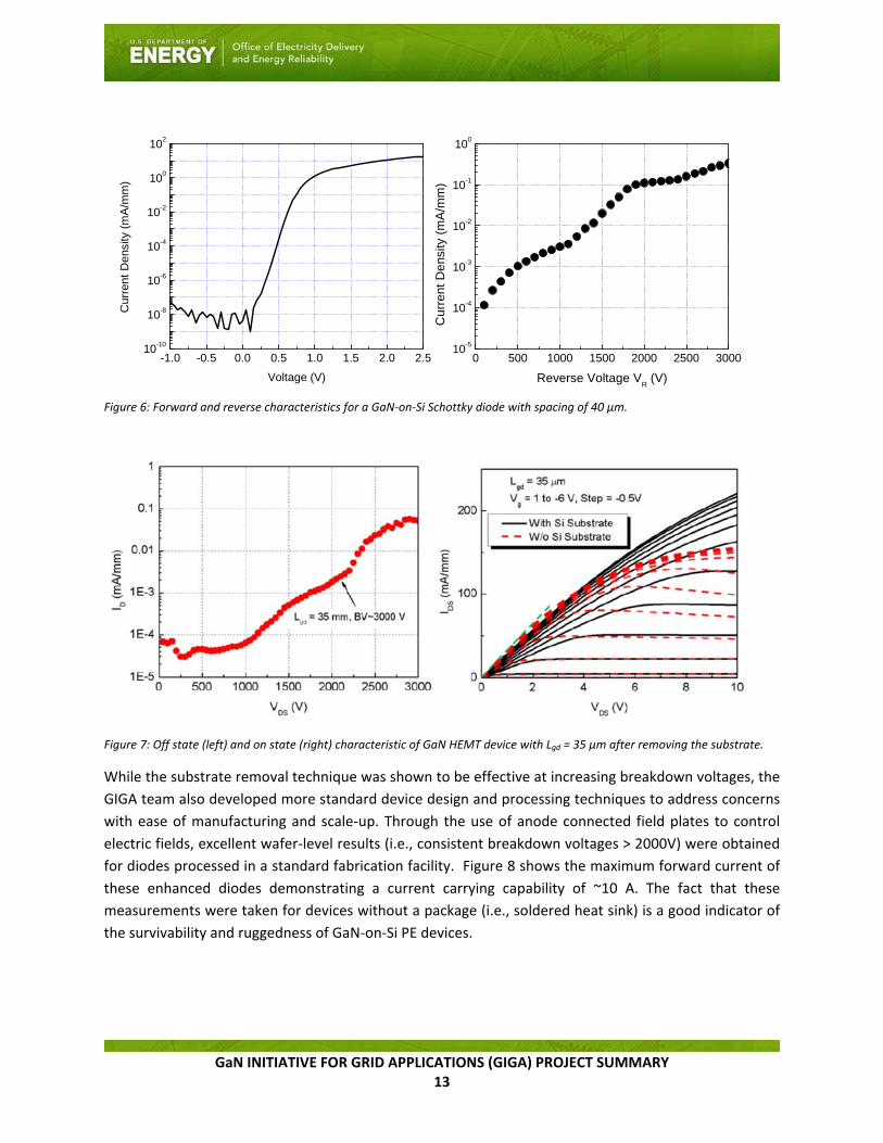
To increase the operating voltage of GaN‐on‐Si PE devices, the GIGA team experimented with several
device fabrication techniques. Silicon substrate removal and device transfer processes were developed to
minimize parasitic leakage currents. By utilizing these technique, diode breakdown voltages > 3000 V were
observed (see Figure 6), which was limited by the test equipment. Additionally, experiments with local
substrate removal (i.e., removing the silicon only under the gate) also showed excellent results, offering
an approach that is more amenable to cost‐effective manufacturing. Experiences with high‐volume LED
manufacturing processes give an indication that substrate removal could be scalable and cost‐effective
with GaN‐on‐Si PE devices. With further development of these device fabrication techniques, the GIGA
team was able to demonstrate ~3000V HEMT devices (i.e., transistors), as shown in Figure 7.
Achievements: Device Development
Established GaN‐on‐Si technology as a viable
option for high power PE devices
Demonstrated GaN‐on‐Si diodes and transistors
with >3 kV and >15 A
Developed advanced fabrication processes and
device architectures including silicon removal
techniques and field plate technology
Investigated and fully characterized breakdown
mechanisms in GaN‐on‐Si device structures
Improved understanding of power device design
and optimization, especially electric field control
GaN INITIATIVE FOR GRID APPLICATIONS (GIGA) PROJECT SUMMARY
13
Figure 6: Forward and reverse characteristics for a GaN‐on‐Si Schottky diode with spacing of 40 µm.
Figure 7: Off state (left) and on state (right) characteristic of GaN HEMT device with Lgd = 35 µm after removing the substrate.
While the substrate removal technique was shown to be effective at increasing breakdown voltages, the
GIGA team also developed more standard device design and processing techniques to address concerns
with ease of manufacturing and scale‐up. Through the use of anode connected field plates to control
electric fields, excellent wafer‐level results (i.e., consistent breakdown voltages > 2000V) were obtained
for diodes processed in a standard fabrication facility. Figure 8 shows the maximum forward current of
these enhanced diodes demonstrating a current carrying capability of ~10 A. The fact that these
measurements were taken for devices without a package (i.e., soldered heat sink) is a good indicator of
the survivability and ruggedness of GaN‐on‐Si PE devices.
-1.0 -0.5 0.0 0.5 1.0 1.5 2.0 2.510-10
10-8
10-6
10-4
10-2
100
102
C
urre
nt D
ensi
ty (
mA
/mm
)
Voltage (V)
0 500 1000 1500 2000 2500 300010-5
10-4
10-3
10-2
10-1
100
Cu
rre
nt D
ens
ity (
mA
/mm
)
Reverse Voltage VR (V)
GaN INITIATIVE FOR GRID APPLICATIONS (GIGA) PROJECT SUMMARY
14
Figure 8: Linear Plot of the Forward Characteristic of Lateral GaN‐on‐Si Schottky Diodes having a total Anode Periphery of 20.0 mm and 10 μm to 30 μm Anode‐to‐Cathode Spacings
The GIGA team also explored the use of multi‐level field plates (see Figure 9) to properly control high
electrical fields present in GaN HEMT devices, as well as leveraging multi‐finger device designs to increase
current carrying capabilities. Effective electric field engineering was recognized as critical for achieving
even higher voltage operation. By utilizing advanced field plate structures, the GIGA team demonstrated
GaN‐on‐Si transistor breakdown voltages of ~2000 V. Another important benefit of the advanced field
plate structures is suppression of the gate‐to‐drain leakage currents (up to 10,000X observed). These
enhanced GaN HEMT devices demonstrated a maximum normalized current of ~0.7 A/mm when soldered
in a RF package (as there was no suitable power package), a > 40% improvement over unpackaged devices.
If these GaN‐on‐Si transistors were produced with a 30 mm gate periphery and proper packaging, > 20 A
of current handling capability could be readily achieved.
Figure 9: Conceptual Cross section of GaN HEMT device with Gate Connected and Source Connected Field Plates
GaN INITIATIVE FOR GRID APPLICATIONS (GIGA) PROJECT SUMMARY
15
EnhancedManufacturabilityforEnd‐UseProductIn addition to improving foundational wafer
materials and demonstrating critical proofs‐of‐
concept, the project made significant advances to
enhance manufacturability so that GaN‐on‐Si PE
devices can be integrated into products that
would be broadly adopted by industry. The GIGA
team developed technologies and processes to
form gold‐free, low resistance Ohmic contacts
with low annealing temperatures in GaN‐on‐Si PE
device. This key breakthrough allowed GaN‐on‐Si
devices to be manufactured on standard high‐
throughput silicon integrated circuit fabrication
lines without risking contamination. Additionally,
the GIGA team demonstrated the fabrication and
operation of enhancement mode (i.e., normally off) transistors using an innovative dual‐gate technology.
Availability of GaN‐on‐Si enhancement mode transistors ensures safe switching operations and is required
for broad acceptance and use of GaN‐on Si PE devices in products sold by the power electronics industry.
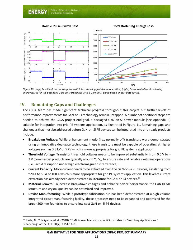
The GIGA team also conducted dynamic testing of packaged GaN‐on‐Si transistors to extract switching
losses, an important product specification, and to understand drive circuit design requirements. Transistor
turn‐on times of 15 nanosecond and turn‐off times of 20 nanoseconds were recorded, demonstrating very
fast switching operations (see Figure 10). However, unavailability of optimized packaging for GaN‐on‐Si
PE devices presents challenges for adoption in real‐world applications and will need to be addressed.
Packaged GaN‐on‐Si diodes were also operated with the GaN‐on‐Si transistors in a test circuit showing
improved performance compared to the use of a SiC diode. The data shows a decrease in total switching
energy losses of approximately 5% with the GaN‐on‐Si diode. This result suggests there can be great
synergy from integrating transistors and diodes in the same fabrication process, which is much more
amenable with GaN‐on‐Si lateral device geometries.
Achievements: Enhanced Manufacturability
First gold‐free GaN‐on‐Si process technology
Prototype production runs of GaN‐on‐Si PE devices
in a 100 mm fabrication facility with good
performance and yield
All technologies have been licensed to start‐ups
and other companies
Demonstrated “normally off” device architectures
for safer switching operations
Conducted dynamic testing of packaged devices to
extract switching losses
Demonstrated operation of GaN‐on‐Si transistors
with GaN‐on‐Si diodes for improved performance
GaN INITIATIVE FOR GRID APPLICATIONS (GIGA) PROJECT SUMMARY
16
Figure 10: (left) Results of the double pulse switch test showing fast device operation; (right) Extrapolated total switching energy losses for the packaged GaN‐on‐Si transistor with a GaN‐on‐Si diode based on test data (ORNL)
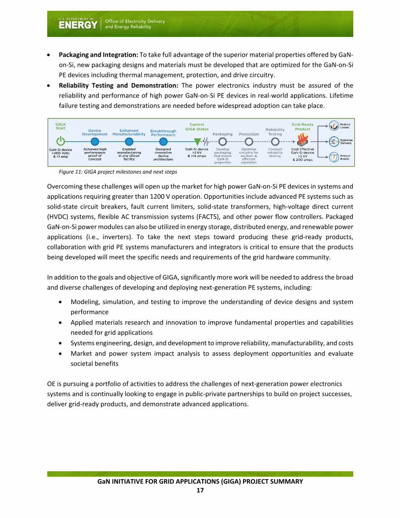
IV. RemainingGapsandChallengesThe GIGA team has made significant technical progress throughout this project but further levels of
performance improvements for GaN‐on‐Si technology remain untapped. A number of additional steps are
needed to achieve the GIGA project end goal, a packaged GaN‐on‐Si power module (see Appendix B)
suitable for integration into grid PE systems application, as illustrated in Figure 11. Remaining gaps and
challenges that must be addressed before GaN‐on‐Si PE devices can be integrated into grid‐ready products
include:
Breakdown Voltage: While enhancement mode (i.e., normally off) transistors were demonstrated
using an innovative dual‐gate technology, these transistors must be capable of operating at higher
voltages such as 3.3 kV or 5 kV which is more appropriate for grid PE systems application.
Threshold Voltage: Transistor threshold voltages needs to be improved substantially, from 0.5 V to >
2 V (commercial products are typically around ~3 V), to ensure safe and reliable switching operations
(i.e., avoid disruption under high electromagnetic interference).
Current Capacity: More current needs to be extracted from the GaN‐on‐Si PE devices, escalating from
~20 A to 50 A or 100 A which is more appropriate for grid PE systems application. This level of current
extraction has already been demonstrated in literature for GaN‐on‐Si devices.24
Material Growth: To increase breakdown voltages and enhance device performance, the GaN HEMT
structure and crystal quality can be optimized and improved.
Device Manufacturing: While a prototype fabrication run has been demonstrated at a high‐volume
integrated circuit manufacturing facility, these processes need to be expanded and optimized for the
larger 200 mm foundries to ensure low cost GaN‐on‐Si PE devices.
24 Ikeda, N., Y. Niiyama, et al. (2010). "GaN Power Transistors on Si Substrates for Switching Applications." Proceedings of the IEEE 98(7): 1151‐1161.
GaN INITIATIVE FOR GRID APPLICATIONS (GIGA) PROJECT SUMMARY
17
Packaging and Integration: To take full advantage of the superior material properties offered by GaN‐
on‐Si, new packaging designs and materials must be developed that are optimized for the GaN‐on‐Si
PE devices including thermal management, protection, and drive circuitry.
Reliability Testing and Demonstration: The power electronics industry must be assured of the
reliability and performance of high power GaN‐on‐Si PE devices in real‐world applications. Lifetime
failure testing and demonstrations are needed before widespread adoption can take place.
Figure 11: GIGA project milestones and next steps
Overcoming these challenges will open up the market for high power GaN‐on‐Si PE devices in systems and
applications requiring greater than 1200 V operation. Opportunities include advanced PE systems such as
solid‐state circuit breakers, fault current limiters, solid‐state transformers, high‐voltage direct current
(HVDC) systems, flexible AC transmission systems (FACTS), and other power flow controllers. Packaged
GaN‐on‐Si power modules can also be utilized in energy storage, distributed energy, and renewable power
applications (i.e., inverters). To take the next steps toward producing these grid‐ready products,
collaboration with grid PE systems manufacturers and integrators is critical to ensure that the products
being developed will meet the specific needs and requirements of the grid hardware community.
In addition to the goals and objective of GIGA, significantly more work will be needed to address the broad
and diverse challenges of developing and deploying next‐generation PE systems, including:
Modeling, simulation, and testing to improve the understanding of device designs and system
performance
Applied materials research and innovation to improve fundamental properties and capabilities
needed for grid applications
Systems engineering, design, and development to improve reliability, manufacturability, and costs
Market and power system impact analysis to assess deployment opportunities and evaluate
societal benefits
OE is pursuing a portfolio of activities to address the challenges of next‐generation power electronics
systems and is continually looking to engage in public‐private partnerships to build on project successes,
deliver grid‐ready products, and demonstrate advanced applications.
GaN INITIATIVE FOR GRID APPLICATIONS (GIGA) PROJECT SUMMARY
18
AppendixA:FullGIGAPublicationsList
[1] B. Lu, E. L. Piner, and T. Palacios, “Breakdown mechanism in AlGaN/GaN HEMTs on Si substrate,”
Proc. Of the 68th Device Research Conference, Notre Dame, IN, June 21‐23, 2010.
[2] Timothy Boles, Costas Varmazis, Douglas Carlson, Tomas Palacios, “Effect of Isolation
Techniques on GaN on Silicon Breakdown Voltage”, International Workshop on Nitrides,
September, 2010
[3] B. Lu, E. L. Piner, and T. Palacios, “High Performance Dual‐Gate AlGaN/GaN Enhancement‐Mode
Transistor,” Proc. Of the International Symposium on Compound Semiconductors (ISCS‐2010),
Takamatsu, Japan, May 31st‐June 4th, 2010.
[4] B. Lu and T. Palacios, “High Performance Dual‐Gate AlGaN/GaN Enhancement‐Mode
Transistor”, IEEE Elec. Dev. Lett., vol. 31, no. 9, p. 990, September 2010.
[5] B. Lu and T. Palacios, “High Breakdown (>1500 V) AlGaN/GaN HEMTs by Substrate Transfer
Technology”, IEEE Elec. Dev. Lett., vol. 31, no. 9, p. 951, September 2010
[6] Lu, B., E. L. Piner, and T. Palacios, “Schottky Drain Technology for High Voltage AlGaN/GaN
HEMTs on Si Substrates,” IEEE Electron Dev. Letts., vol. 31, 302‐304, 2010.
[7] B. Lu, D. Piedra, and T. Palacios, "GaN power electronics," in 18th International Conference on
Advanced Semiconductor Devices and Microsystems, ASDAM 2010, October 25, 2010 ‐ October
27, 2010, Smolenice, Slovakia, 2010, pp. 105‐110.
[8] M. Sun, H.S. Lee, B. Lu, D. Piedra, E. Matioli, and T. Palacios, “1.8kV‐breakdown AlGaN/GaN
HEMT on Si substrate with Ron=2.4mΩcm2”, in the 9th International Conference on Nitride
Semiconductors (ICNS‐9), July, 2011, Glasgow, UK, 2011.
[9] H.‐S. Lee, D. Lee, and T. Palacios, “AlGaN/GaN High‐Electron‐Mobility Transistors Fabricated
Through a Au‐free Technology,” IEEE Electron Device Letters, v 32, 623‐625, May 2011.
[10] M. Sun, H.S. Lee, B. Lu, D. Piedra, and T. Palacios, “1.8 kV‐Breakdown AlGaN/GaN HEMT on Si
Substrate with Ion Implantation Isolation”, submitted to IEEE Electron Device Letters.
[11] D. Piedra, T. G. Desai, R. Bonner, J. Pascaul‐Guiterrez, M. Sun, and T. Palacios, “Integration of a
Phase Change Material for Junction Level Cooling in GaN Devices”, submitted to the 28th Annual
Thermal Measurement, Modeling and Management Symposium (SEMI‐THERM 28), 2012.
[12] H. S. Lee, D. Piedra, M. Sun, X. Gao, S. P. Guo, T. Palacios, “3000 V 4.3 cm2 InAlN/GaN
MOSHEMTs with AlGaN Back Barrier,” IEEE Electron Dev. Letts., vol. 33, pp. 982‐984, 2012.
[13] S. Atcitty, R. Kaplar, S. Das Gupta, M. Marinella, A. Armstrong, L. Biederman, M. Sun, T. Palacios,
and M. Smith, “GaN‐Based Wide‐Bandgap Power Switching Devices: From Atoms to the Grid”
ECS Transactions, 50, (3) , 2012
GaN INITIATIVE FOR GRID APPLICATIONS (GIGA) PROJECT SUMMARY
19
[14] D. Piedra, T. G. Desai, R. Bonner, J. Pascaul‐Guiterrez, M. Sun, and T. Palacios, “Integration of a
Phase Change Material for Junction Level Cooling in GaN Devices”, to be published in the 28th
Annual Thermal Measurement, Modeling and Management Symposium (SEMI‐THERM 28)
[15] T. Boles, C. Varmazis, D. Carlson, T. Palacios, G. Turner, and R. Molnar, “High Voltage GaN on
Silicon HEMT”, accepted as a poster presentation at ISCS 2012.
[16] T. Boles, C. Varmazis, D. Carlson, T. Palacios, G. Turner, and R. Molnar,”>1200 volt GaN on Silicon
Schottky Diode”, accepted as an oral presentation at ISCS 2012..
[17] B. Lu, E. Matioli and T. Palacios, “Tri‐gate Normally‐Off Power MISHEMT,” IEEE Electron Dev.
Letts., vol. 33, 360‐362, 2012.
[18] H.‐S. Lee, D. Piedra, M. Sun, X. Gao, S. Guo, T. Palacios, “3000‐V 4.3‐mΩ•cm2 InAlN/GaN
MOSHEMTs With AlGaN Back Barrier,” IEEE Electron Device Letters, v 33, 982‐984, July 2012.
[19] M. Sun, H.S. Lee, B. Lu, D. Piedra, and T. Palacios, “Comparative breakdown study of mesa‐ and
ion‐implantation‐isolated AlGaN/GaN high‐electron‐mobility transistors on Si substrate”, Appl.
Phys. Express, vol.7, 074202, 2012.
[20] S. Atcitty, R. Kaplar, S. Das Gupta, M. Marinella, A. Armstrong, L. Biederman, M. Sun, T. Palacios,
and M. Smith, “GaN‐Based Wide‐Bandgap Power Switching Devices: From Atoms to the Grid”
ECS Transactions, 50, (3), 2012.
[21] T. Boles, C. Varmazis, D. Carlson, T. Palacios, G. W. Turner, R. J. Molnar, “>1200 volt GaN‐on‐
Silicon Schottky Diode”, International Symposium on Compound Semiconductors 2012, August,
2012.
[22] T. Boles, C. Varmazis, D. Carlson, T. Palacios, G. W. Turner, R. J. Molnar, “High Voltage GaN‐on‐
Silicon HEMT”, International Symposium on Compound Semiconductors 2012, August, 2012.
[23] T. Boles, C. Varmazis, D. Carlson, T. Palacios, G. W. Turner, R.J. Molnar, “High Voltage GaN‐on‐
Silicon HEMT, Physica Status Solidi, January, 2013.
[24] T. Boles, C. Varmazis, D. Carlson, T. Palacios, G. W. Turner, R.J. Molnar, “GaN‐on‐Silicon High
Voltage Schottky Diode”, Physica Status Solidi, April, 2013.
[25] T. Boles, D. Carlson, T. Palacios, M. Soboroff, “Cost Effective, High Performance GaN
Technology”, Compound Semiconductor Magazine, April, 2013.
[26] T. Boles, C. Varmazis, D. Carlson, T. Palacios, G. W. Turner, R.J. Molnar, “GaN‐on‐Silicon High
Voltage Schottky Diode”, Physica Status Solidi, April, 2013.
[27] T. Boles, C. Varmazis, D. Carlson, L. Xia, D. Jin, T. Palacios, G. W. Turner, R. J. Molnar, “High‐
Voltage GaN‐on‐Silicon Schottky Diodes”, CSMANTECH, May, 2013.
[28] T. Boles, C. Varmazis, D. Carlson, L. Xia, D. Jin, T. Palacios, G. W. Turner, R. J. Molnar, “High
Voltage GaN‐on‐Silicon HEMT’s”, CSMANTECH, May, 2013
GaN INITIATIVE FOR GRID APPLICATIONS (GIGA) PROJECT SUMMARY
20
[29] Y. Zhang, M. Sun, T. Fujishima, Z. Liu, K. Bagnall, D. Piedra, E. Wang, and T. Palacios, “Electro‐
thermal Modeling and Thermal Performance Study of GaN Vertical and Lateral Power
Transistors,” IEEE Trans. Electron Dev., vol. 63, 2224‐2230, July 2013.
[30] S. DasGupta, R.J. Kaplar, M. Sun, M.J. Marinella, S. Atcitty, and T. Palacios “Effect of Interaction
of Deep Level Defects with Quantum Well States on Detrapping Transients in High‐Voltage
AlGaN/GaN HEMTs” Abstract #1943 224th ECS Meeting, 2013.
[31] T. Boles, D. Carlson, L. Xia, A. Kaleta, C. McLean, D. Jin,T. Palacios, G. W. Turner and R. J. Molnar,
“Effect of Multi‐Field Plates on GaN‐on‐Silicon HEMTs “,CSMANTECH 2014.
[32] S. DasGupta, M. Sun, A. Armstrong, R. J. Kaplar, M. J. Marinella, J. B. Stanley, S. Atcitty, and T.
Palacios, “Slow Detrapping Transients due to Gate and Drain Bias Stress in High Breakdown
Voltage AlGaN/GaN HEMTs,” IEEE Trans. Elec. Dev. 59 (8), 2115 (2012).
[33] S. DasGupta, L. B. Biedermann, M. Sun, R. Kaplar, M. Marinella, K. R. Zavadil, S. Atcitty, and T.
Palacios, “Role of Barrier Structure in Current Collapse of AlGaN/GaN High Electron Mobility
Transistors,” Appl. Phys. Lett. 101, 243506 (2012).
[34] S. DasGupta, A. Armstrong, R. Kaplar, M. Marinella, J. Stanley, M. Smith, S. Atcitty, M. Sun, and
T. Palacios, "Impact of the Al Mole Fraction on the Bulk‐ and Surface‐State‐Induced Instability
of AlGaN/GaN HEMTs," MRS Proc. 1432, 151 (Spring 2012).
[35] R. Kaplar, M. Marinella, S. DasGupta, M. Smith, S. Atcitty, M. Sun, and T. Palacios,
“Characterization and Reliability of SiC‐ and GaN‐Based Power Transistors for Renewable Energy
Applications,” Proc. IEEE Energy Tech (2012).
[36] S. Atcitty, R. Kaplar, S. DasGupta, M. Marinella, A. Armstrong, L. Biedermann, M. Sun, T. Palacios,
and M. Smith, “GaN‐Based Wide‐Bandgap Power Switching Devices: From Atoms to the Grid,”
ECS Trans. 50 (3), 199 (2012).
[37] S. DasGupta, L. Biedermann, M. Sun, R. K. Kaplar, M. J. Marinella, K. Zavadil, S. Atcitty, and T.
Palacios, “Influence of Barrier Design on Current Collapse in High Voltage AlGaN/GaN HEMTs,”
Proc. IEEE IRPS, 3C.4 (2013).
[38] M. J. Marinella, S. DasGupta, R. J. Kaplar, M. Sun, S. Atcitty, and T. Palacios, “Interaction of
Defects with Quantum Well States: Electrostatic‐Dependent Response Time for Traps in
AlGaN/GaN HEMTs,” ECS Trans. 58 (4), 365 (2013)
[39] Lu, B., and T. Palacios, “Schottky‐Drain Technology for High Breakdown Voltage AlGaN/GaN
HEMTs on Si Substrate,” International Conference on Nitride Semiconductors, Jeju Island, South
Korea, 2 pages, 18‐23 October 2009.
[40] Lu, B. and T. Palacios, “High Performance Dual‐Gate AlGaN/GaN Enhancement‐Mode
Transistor,” 37th International Symposium on Compound Semiconductors (ISCS), Takamatsu
Symbol Tower, Kagawa, Japan, 31 May – 4 June 2010.
GaN INITIATIVE FOR GRID APPLICATIONS (GIGA) PROJECT SUMMARY
21
[41] Lu, B. and T. Palacios, “Breakdown Mechanism in AlGaN/GaN HEMTs on Si Substrate,” 68th
Device Research Conference, South Bend, IN, 21‐23 June 2010.
[42] Lee, D. S., R. Molnar, C. Hatem, X. Gao, S. Guo, and T. Palacios, “Ultralow Contact Resistance in
InAlN/GaN Heterostructures Through Si Ion Implantation,” International Workshop on Nitride
Semiconductors (IWN‐2010), Tampa, FL, 19‐24 September 2010.
[43] Palacios, T., “GaN‐on‐Si Technology, A New Approach for Advanced Devices in Energy and
Communications,” 40th European Solid‐State Device Research Conference (ESSDERC), Seville,
Spain, 13‐17 September 2010. (Invited)
[44] Palacios, T., “GaN Power Electronics,” 8th International Conference on Advanced
Semiconductor Devices and Microsystems (ASDAM 2010), Smolenice, Slovakia, 25‐27 October
2010. (Invited)
[45] M. Sun, H.S. Lee, B. Lu, D. Piedra, E. Matioli, and T. Palacios, “1.8kV‐breakdown AlGaN/GaN
HEMT on Si substrate with Ron=2.4mΩcm2”, in the 9th International Conference on Nitride
Semiconductors (ICNS‐9), July, 2011, Glasgow, UK, 2011.
[46] D. Piedra, T. G. Desai, R. Bonner, J. Pascaul‐Guiterrez, M. Sun, and T. Palacios, “Integration of a
Phase Change Material for Junction Level Cooling in GaN Devices”, oral presentation at 28th
Annual Thermal Measurement, Modeling and Management Symposium (SEMI‐THERM 28).
[47] Y. Zhang, M. Sun, T. Fujishima, K. Bagnall, Z. Liu, E. Wang, and T. Palacios, “Thermal Performance
of GaN Vertical and Lateral Power Transistors”, accepted for oral presentation at International
Workshop on Nitride Semiconductors (IWN‐2012), Sapporo, Japan, October 2012.
[48] D. Piedra, H.‐S. Lee, T. Palacios, X. Gao, and S. Guo, “Scaling of InAlN/GaN Power Transistors,”
accepted for oral presentation at 42th European Solid‐State Device Research Conference
(ESSDERC), Nice, France, September 2012.
[49] D. Piedra, H.‐S. Lee, X. Gao, S. Guo, and T. Palacios, “Impact of InGaN Back‐barrier on the
Breakdown Voltage of InAlN/GaN HEMTs.” accepted for oral presentation at International
Workshop on Nitride Semiconductors (IWN‐2012), Sapporo, Japan, October 2012.
[50] Palacios, T., “GaN Transistors: Revolutionizing Energy Processing,” 4th International Symposium
on Advanced Plasma Science and its Applications to Nitrides and Nanomaterials, Aichi, Japan,
March 4‐8, 2012. (Invited).
[51] T. Palacios, “Fundamentals of GaN‐based High Frequency Power Electronics,” Tutorial at the
International Electron Device Meeting, San Francisco, December, 2012.
[52] T. Palacios, “GaN Devices for the Next Generation of Power Electronics,” Spring Meeting of the
Materials Research Society, San Francisco, CA, April 4, 2013.
[53] B. Lu, M. Sun, and T. Palacios, “An Etch‐Stop Barrier Structure for GaN High Electron Mobility
Transistors,” IEEE Electron Dev. Letts., vol. 34, pp. 369‐371, 2013.
GaN INITIATIVE FOR GRID APPLICATIONS (GIGA) PROJECT SUMMARY
22
[54] X. Sun, O. I. Saadat, K. S. Chang‐Liao, T. Palacios, S. Cui, and T. P. Ma, “Study of Gate Oxide Traps
in HfO2/AlGaN/GaN metal‐oxide‐semiconductor high electron mobility transistors by use of ac
transconductance method,” Appl. Phys. Letts., vol. 102, pp. 103504, 2013.
[55] X. W. Wang, O. I. Saadat, B. Xi, X. B. Lou, R. J. Molnar, T. Palacios, and R. G. Gordon, “Atomic
layer deposition of Sc2O3 for passivating AlGaN/GaN high electron mobility transistor devices,”
Appl. Phys. Letts., vol. 101, pp. 232109, 2012.
[56] Timothy Boles, Douglas Carlson, Mike Soboroff, and Tomas Palacios, “Boosting GaN‐on‐silicon
blocking voltages”, Compound Semiconductor, May 20 2013.
GaN INITIATIVE FOR GRID APPLICATIONS (GIGA) PROJECT SUMMARY
23
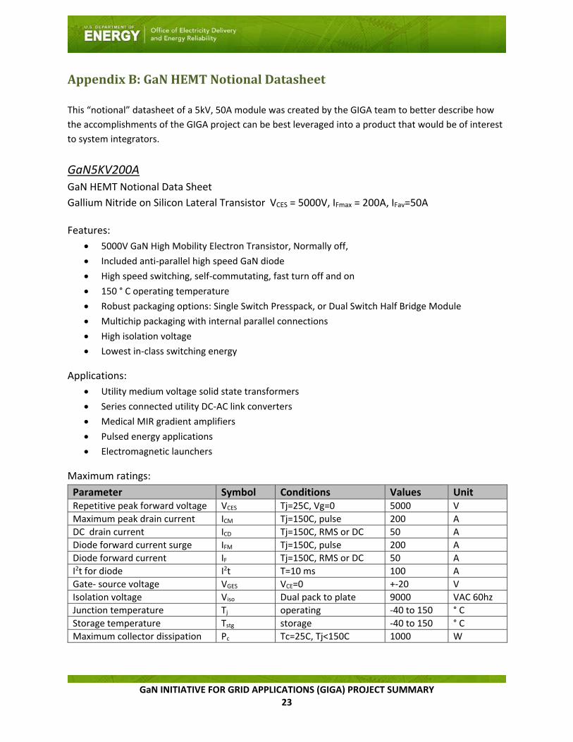
AppendixB:GaNHEMTNotionalDatasheet
This “notional” datasheet of a 5kV, 50A module was created by the GIGA team to better describe how
the accomplishments of the GIGA project can be best leveraged into a product that would be of interest
to system integrators.
GaN5KV200A
GaN HEMT Notional Data Sheet
Gallium Nitride on Silicon Lateral Transistor VCES = 5000V, IFmax = 200A, IFav=50A
Features:
5000V GaN High Mobility Electron Transistor, Normally off,
Included anti‐parallel high speed GaN diode
High speed switching, self‐commutating, fast turn off and on
150 ° C operating temperature
Robust packaging options: Single Switch Presspack, or Dual Switch Half Bridge Module
Multichip packaging with internal parallel connections
High isolation voltage
Lowest in‐class switching energy
Applications:
Utility medium voltage solid state transformers
Series connected utility DC‐AC link converters
Medical MIR gradient amplifiers
Pulsed energy applications
Electromagnetic launchers
Maximum ratings:
Parameter Symbol Conditions Values Unit Repetitive peak forward voltage VCES Tj=25C, Vg=0 5000 V
Maximum peak drain current ICM Tj=150C, pulse 200 A
DC drain current ICD Tj=150C, RMS or DC 50 A
Diode forward current surge IFM Tj=150C, pulse 200 A
Diode forward current IF Tj=150C, RMS or DC 50 A
I2t for diode I2t T=10 ms 100 A
Gate‐ source voltage VGES VCE=0 +‐20 V
Isolation voltage Viso Dual pack to plate 9000 VAC 60hz
Junction temperature Tj operating ‐40 to 150 ° C
Storage temperature Tstg storage ‐40 to 150 ° C
Maximum collector dissipation Pc Tc=25C, Tj<150C 1000 W
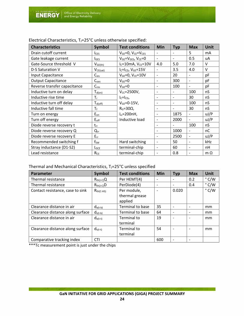
GaN INITIATIVE FOR GRID APPLICATIONS (GIGA) PROJECT SUMMARY
24
Electrical Characteristics, TJ=25°C unless otherwise specified:
Characteristics Symbol Test conditions Min Typ Max Unit Drain cutoff current ICES VGE=0, VCE=VCES ‐ ‐ 5 mA
Gate leakage current IGES VGE=VGES, VCE=0 ‐ ‐ 0.5 uA
Gate‐Source threshold V VGE(th) IC=10mA, VCE=10V 4.0 5.0 7.0 V
D‐S Saturation V VCE(sat) IC=ICD, VGE=15V ‐ 3.5 4.0 V
Input Capacitance Cies VGE=0, VCE=10V ‐ 20 ‐ pF
Output Capacitance Coes VGE=0 ‐ 300 ‐ pF
Reverse transfer capacitance Cres VGE=0 ‐ 100 ‐ pF
Inductive turn on delay Td(on) VCC=2500V, ‐ ‐ 100 nS
Inductive rise time Tr IC=ICD, ‐ ‐ 30 nS
Inductive turn off delay Td(off) VGE=0‐15V, ‐ ‐ 100 nS
Inductive fall time Tf RG=30Ω, ‐ ‐ 30 nS
Turn on energy Eon Ls=200nH, ‐ 1875 ‐ uJ/P
Turn off energy Eoff Inductive load ‐ 2000 ‐ uJ/P
Diode reverse recovery t trr ‐ ‐ 100 nS
Diode reverse recovery Q Qrr ‐ 1000 ‐ nC
Diode reverse recovery E Err ‐ 2500 ‐ uJ/P
Recommended switching f fSW Hard switching ‐ 50 ‐ kHz
Stray inductance (D1‐S2) LSCE terminal‐chip ‐ 60 ‐ nH
Lead resistance RCE terminal‐chip ‐ 0.8 ‐ m Ω
Thermal and Mechanical Characteristics, TJ=25°C unless specified
Parameter Symbol Test conditions Min Typ Max Unit Thermal resistance Rth(J‐C)Q Per HEMT(4) ‐ ‐ 0.2 ° C/W
Thermal resistance Rth(J‐C)D PerDiode(4) ‐ ‐ 0.4 ° C/W
Contact resistance, case to sink Rth(C‐HS) Per module, thermal grease applied
‐ 0.020 ° C/W
Clearance distance in air da(t‐b) Terminal to base 35 ‐ ‐ mm
Clearance distance along surface ds(t‐b) Terminal to base 64 ‐ ‐ mm
Clearance distance in air da(t‐t) Terminal to terminal
19 ‐ ‐ mm
Clearance distance along surface ds(t‐t) Terminal to terminal
54 ‐ ‐ mm
Comparative tracking index CTI 600 ‐ ‐
***Tc measurement point is just under the chips
GaN INITIATIVE FOR GRID APPLICATIONS (GIGA) PROJECT SUMMARY
25
Packaging Option A: Presspack, Dual sided cooling, Creepage and Clearance meet IEC 60077‐1
Packaging Option B: Dual HV Module, Isolated Base, Creepage and Clearance meet IEC 60077‐1