Contents IC technology Lithographyhome.agh.edu.pl/~marszale/downloads/W3_Lithografia.pdf · IC...
22
Course IC technology - file lithography.ppt 31 January 2000 Leerstoel Halfgeleider Componenten 1 IC technology Lithography IC technology: Lithography 2 Contents 1. Introduction 2. Overall lithography process 3. Light sources 4. Optical exposure systems 5. Resist materials 6. Optics basics 7. Resolution improvement 8. Advanced lithography – X-Ray lithography – Electron beam lithography – SCALPEL – EUV 9. Summary
Transcript of Contents IC technology Lithographyhome.agh.edu.pl/~marszale/downloads/W3_Lithografia.pdf · IC...

Course IC technology - file lithography.ppt 31 January 2000
Leerstoel Halfgeleider Componenten 1
IC technology
Lithography
IC technology: Lithography 2
Contents
1. Introduction
2. Overall lithography process
3. Light sources4. Optical exposure systems5. Resist materials
6. Optics basics7. Resolution improvement
8. Advanced lithography– X-Ray lithography– Electron beam lithography– SCALPEL– EUV
9. Summary

Course IC technology - file lithography.ppt 31 January 2000
Leerstoel Halfgeleider Componenten 2
IC technology: Lithography 3
1. Introduction1.1. Lithography: basic concept
• Spin-onphotoresist
• Expose locally with UV light
• Developphotoresist
UV-light
mask
photo-resist
silicon oxide
silicon substrate
IC technology: Lithography 4
1.2. Lithography: demands
• Resolution requirements– smaller device structures
• Exposure field requirements– increasing chip size, need to
exposure at least one full chip with each exposure
• Placement accuracy– each mask layer needs to be carefully
aligned with respect to the existing pattern
• Throughput– translates into manufacturing costs
• Defect density– Translates into yield loss and higher
costs for the finished chips

Course IC technology - file lithography.ppt 31 January 2000
Leerstoel Halfgeleider Componenten 3
IC technology: Lithography 5
1.3. Lithography: roadmap
• Miniaturisation:– More functions per chip– Increasing speed– Reduction of costs
⇒ Can be realised by lithography improvements
IC technology: Lithography 6
2. Overall lithography process
Mask making: Pattern on mask
Photoresist on substrateAlignment to previous layers
Exposure of resist - energetic radiation(UV, X-ray, E-beam, Ion, DUV, ….)
Resist development
Process step (etch, implantation, …)
Resist removal
CAD input
litho
grap
hy
Next process steps

Course IC technology - file lithography.ppt 31 January 2000
Leerstoel Halfgeleider Componenten 4
IC technology: Lithography 7
2.1. Computer Aided Design (CAD) systems
• Patterns are designed using CAD systems, which contain:– Libraries of previous design (basic
circuits)– Software tools to wire the connections
between functional blocks– Simulation tools to predict the
performance of the new design
IC technology: Lithography 8
2.2. Mask making
(Mask made in separate mask shop)
• High precision needed
• Cost may be high!
Quartz plate
(chromium layer)

Course IC technology - file lithography.ppt 31 January 2000
Leerstoel Halfgeleider Componenten 5
IC technology: Lithography 9
2.2. Mask making
• Mask writing is usually done with a laser or an electron beam pattern generator:
– rastering a beam in an X-Y pattern across the mask
– 4 or 5 times magnification for step and repeat systems
IC technology: Lithography 10
2.3. Lithography process, wafer exposure
• Actual lithography process can be separated into three parts:
– light sources– associated with the
photoresist
Course IC technology - file lithography.ppt 31 January 2000
Leerstoel Halfgeleider Componenten 6
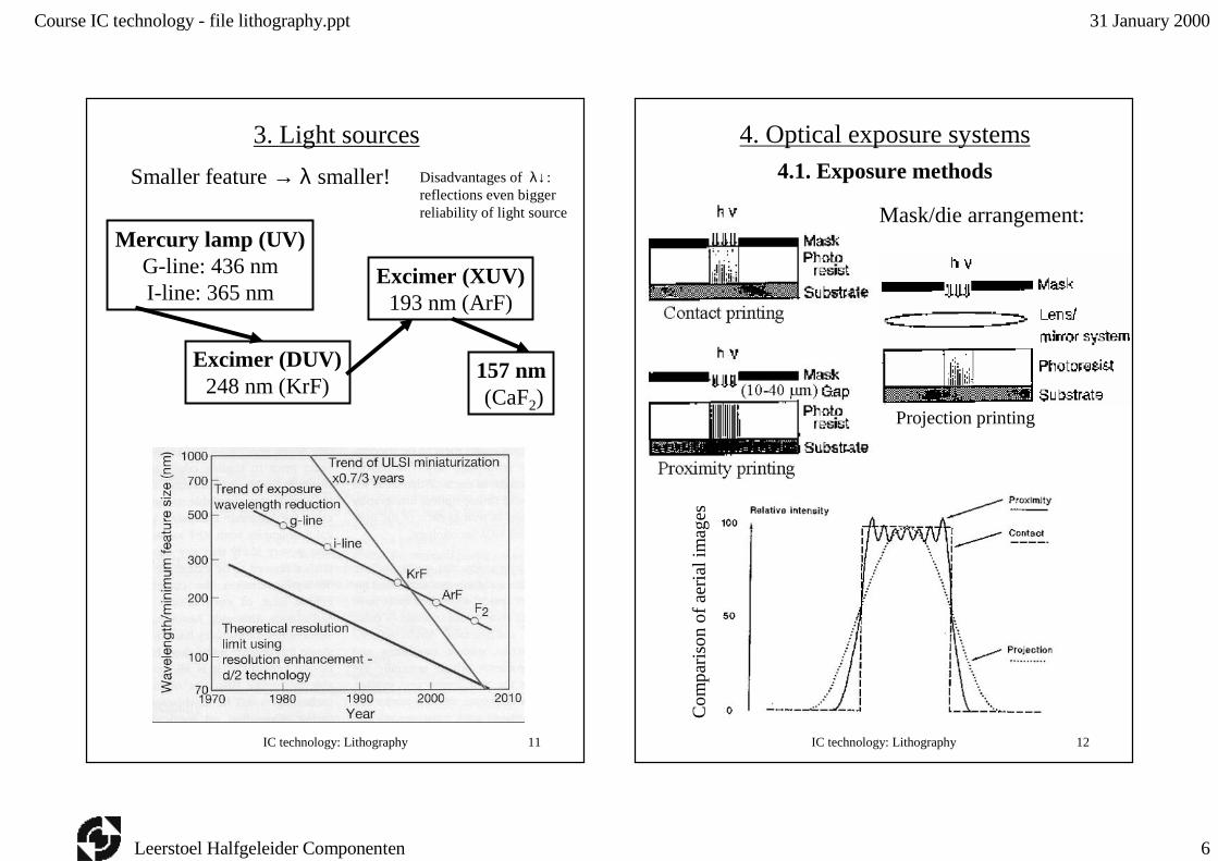
IC technology: Lithography 11
3. Light sources
Smaller feature → λ smaller!
Excimer (XUV)193 nm (ArF)
Excimer (DUV)248 nm (KrF)
Mercury lamp (UV)G-line: 436 nmI-line: 365 nm
Disadvantages of λ↓:reflections even biggerreliability of light source
157 nm(CaF2)
IC technology: Lithography 12
4. Optical exposure systems4.1. Exposure methods
Co
mp
aris
on
of a
eria
l im
ages
Mask/die arrangement:
Projection printing

Course IC technology - file lithography.ppt 31 January 2000
Leerstoel Halfgeleider Componenten 7
IC technology: Lithography 13
4.2. Exposure tools
MESA CR
≈ R ≥ 1.5 µm
poor resolution (≈ 3 µm)mask resolution
mostly used systemR < 1.5 µm
poor-man solution
IC technology: Lithography 14
Step-and-scan systems
• Stepping accomplish the major moves from one exposure field to another
• Within each exposure field, the mask pattern is scanned across the field

Course IC technology - file lithography.ppt 31 January 2000
Leerstoel Halfgeleider Componenten 8
IC technology: Lithography 15
5. Resist materials
• Radiation sensitive compound (organic material) resin + Photoactive compound (PAC) + solvent
• Chemical properties are changed by photochemical reactions
• Two types of resist:
exposed regions disappear exposed regions remain
IC technology: Lithography 16
5.1. Resist properties
• High contrast needed! (resolution)
γ ≈ 2 - 3
• Chemical resistance against many process steps (etchants, implants, …) → resist
• Good adhesion (primer)
1
1
ln:
−
≡
E
EContrast tγ
Course IC technology - file lithography.ppt 31 January 2000
Leerstoel Halfgeleider Componenten 9
IC technology: Lithography 17
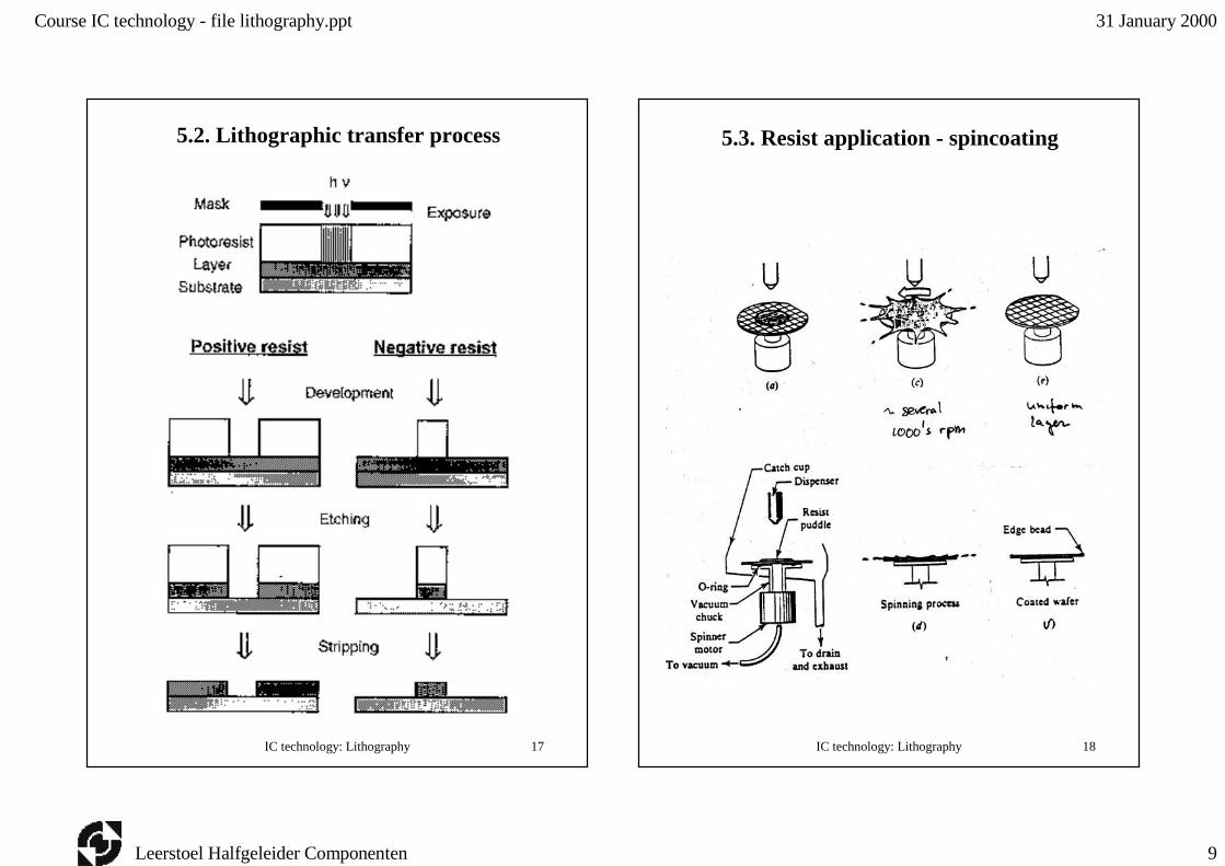
5.2. Lithographic transfer process
IC technology: Lithography 18
5.3. Resist application - spincoating

Course IC technology - file lithography.ppt 31 January 2000
Leerstoel Halfgeleider Componenten 10
IC technology: Lithography 19
Spincoating track
Needed to obtain high reproducibility and high throughput - 50-100 wafers/hour
• spin (3000 - 5000 rpm)• bake• expose• bake
IC technology: Lithography 20
5.4. Typical photoresist process flow

Course IC technology - file lithography.ppt 31 January 2000
Leerstoel Halfgeleider Componenten 11
IC technology: Lithography 21
6. Optics basics6.1. Diffraction
Diameter of central maximum = 1.22λf/d(circular aperture)
IC technology: Lithography 22
6.2. Resolution limit
Minimum feature
(diffraction limited!)
Numerical aperture
αλ
αλλ
sin
61.0
)sin2(
22.122.1
nfn
f
d
fR ===
θsinnNA =NA
kRλ
1=
75.0
6.0
)(248
1 ==
=
k
NA
KrFnmλmR µ31.0=⇒

Course IC technology - file lithography.ppt 31 January 2000
Leerstoel Halfgeleider Componenten 12
IC technology: Lithography 23
6.3. Depth of focus
Increase in resolution leads to a reduction in focus depth
⇒ IC process must be modified when dimensions are reduced!
• More planar surface (planarisation technology)
• Less reflection (anti-reflex coating)
• Thicknesses of layers must be optimised
( ) ↓⇒↑±= DOFRNA
nDOF 22
λ
IC technology: Lithography 24
7. Resolution improvement
• Shorter wavelength
G-line → I-line → DUV → XUV
• Larger NA (≈ 0.5)
• Resist technology (high contrast, AR coatings, …)
• Mask
Optical proximity correction
Phase shift mask
• Non-optical lithography
X-Ray, electron and ion beams
λ ≤ 1-2 Å → no diffraction

Course IC technology - file lithography.ppt 31 January 2000
Leerstoel Halfgeleider Componenten 13
IC technology: Lithography 25
• Anti reflection coatings• Higher resolution resist
7.1. Reflections of the layers
Unwanted reflections on the surface of the chip⇒ undesirable photoresist exposure
IC technology: Lithography 26
7.2. Standing waves
Highly reflective layer below the photoresist
+
Insufficient adsorption of light in the photoresist
=
Interference between the incoming and outgoing waves
⇒ Anti reflection (AR) coatings needed!

Course IC technology - file lithography.ppt 31 January 2000
Leerstoel Halfgeleider Componenten 14
IC technology: Lithography 27
7.3. Optical Proximity Correction (OPC)
• Circular projection systems (lens)
• Rectangular features on masks
High-frequency components of the diffraction pattern are lost
⇒
=> Problem:Aerial image has rounded corners
Solution:Adjust dimensions and shapes on the mask (OPC)
IC technology: Lithography 28
7.4. Phase Shift Mask (PSM)
• Advantages: higher practical resolution and more robust process
• Disadvantages: complex mask, costs (!) and circuit layout design is specific for phase shift
Comparison of aerial image intensity of conventional (left) + Levenson-type PSM (right) mask

Course IC technology - file lithography.ppt 31 January 2000
Leerstoel Halfgeleider Componenten 15
IC technology: Lithography 29
Phase Shift Mask
• Phase Shift Lithography: below 130 nm dimensions (memory)
• mask ≈ 100 k$
IC technology: Lithography 30
PSM: resolution improvement

Course IC technology - file lithography.ppt 31 January 2000
Leerstoel Halfgeleider Componenten 16
IC technology: Lithography 31
(high resolution)
7.5. Resolution enhancement techniques(RET)
• Feature size < wavelength: use RET ⇒ features of approx. λ/2 can be printed
IC technology: Lithography 32
7.6. 157-nm optical lithography
• 157 nm feasible for 100 nm technology?
• Laser source technology?– CaF2 - Calcium fluoride laser – F2 - Fluorine
• Mask?– Fused silica
• Resist?
?

Course IC technology - file lithography.ppt 31 January 2000
Leerstoel Halfgeleider Componenten 17
IC technology: Lithography 33
8. Advanced lithography• Higher resolution than optical lithography
• Sources: photons, electrons, X-rays, ions
• Printing capacities below 70 nm:
– EUV Extreme Ultraviolet Lithography (EUV)
– X-ray proximity
– Ion projection Lithography (IPL)
– SCALPEL (Scattering with angular limitation projection electron-beam lithography)
IC technology: Lithography 34
8.1. X-ray lithography
λ ≈ 1 - 2 Å

Course IC technology - file lithography.ppt 31 January 2000
Leerstoel Halfgeleider Componenten 18
IC technology: Lithography 35
X-ray exposure system
Multiplayer mirror suitable for X-ray reflection
IC technology: Lithography 36
X-ray mask
• Thin membranes (1 µm)
(SiC, SiN, Si, ...)
• Heavy metal absorber
Au, W, ...
• Mask 1:! (very difficult)
• Mechanical stability

Course IC technology - file lithography.ppt 31 January 2000
Leerstoel Halfgeleider Componenten 19
IC technology: Lithography 37
8.2. Electron beam lithography
Very complex equipment (mechanical, electronic, data handling)
Serial process (slow)
Very high resolution (spot size 5 nm) → << 0.1 µm
Well suited for mask fabrication!
IC technology: Lithography 38
E beam resists
PMMA↓
perspex
crosslinking
↓
Also novalak resist(Shipley SAL)

Course IC technology - file lithography.ppt 31 January 2000
Leerstoel Halfgeleider Componenten 20
IC technology: Lithography 39
Proximity effect
Influence of nearby patterns on pattern size!
Isolated line, space, lines/spaces
• Optical proximity effect correction (OPC): uses pre-distorted amplitude patterns at the image plane to compensate for some diffraction effects
Dep
th (µ
m)
20 keV e-beam
0.4 µm resist
IC technology: Lithography 40
SCALPEL
• Scattering Limited Projection Electron Lithography (Lucent)
• +: resolution + printing nature is linear + similar resists as in DUV
• -: difficult mask, little experienceS
catt
erin
g m
ask:
1
00 n
m t
hick
me
mb
ran
e

Course IC technology - file lithography.ppt 31 January 2000
Leerstoel Halfgeleider Componenten 21
IC technology: Lithography 41
8.3. EUV Extreme Ultra-Violet Lithography
• λ≈10 nm, soft X-ray
• all reflective optics, reflective mask
• +: looks most like stepper technology
• -: extremely complex mirror/mask technology
R~ 50 nm!DOF~ 1µm
IC technology: Lithography 42
8.4. Future
• Up to 0.1 µm optical lithography will be used!
• UV to DUV to XUV + tricks
• Phase shift mask• Illumination tricks
• Smaller dimension - ??• EUV, SCALPEL ? → 50 nm
• Continuous improvement of processes
• Stepper• Mask• Resist• Planarisation• Anti-reflection coatings
• (zie Okazaki IEDM ‘96)

Course IC technology - file lithography.ppt 31 January 2000
Leerstoel Halfgeleider Componenten 22
IC technology: Lithography 43
9. Summary
• Lithography:
– Used for reproduction of patterns
– Improvements enable miniaturisation
Mask
• Resist
Equipment
• Optical lithography
– Decreasing wavelength to improve practical resolution
– Resolution Enhancement techniques: print sizes < wavelength, e.g. Phase Shift Mask
• EUV
• SCALPEL