CONTENTS · do not connect the OCP ground (CHB) and the ground AG/LG of the other circuits...
46
l 0 l e 0 CONTENTS (1) SPECIFICATIONS ........................................ 1 (2) DRIVE SECTION BLOCK DIAGRAM ........................... 2 (3) CABLES ................................................ 4 1) CABLE CONNECTIONS FIGURE .......................... 4 2) CABLES ............................................ 5 (4) OUTLINE DRAWINGS ...................................... 8 1) TRANSISTOR AMPLIFIER .............................. 8 2) POWER UNIT ........................................ 9 (5) REPLACING AND HANDLING THE TRANSISTOR AMPLIFIER ....... 10 1) TRANSISTOR AMPLIFIER CONNECTIONS .................. 10 2) CHECKPOINTS BEFORE SWITCHING ON POWER ............. 12 3) CHECKPOINTS ....................................... 13 4) DESCRIPTION OF CHECK PINS ......................... 14 5) DESCRIPTION OF VRS ................................ 20 6) DESCRIPTION OF PLUGS .............................. 22 7) CONNECTOR AND CHECK PIN LAYOUT .................... 25 8) VR LAYOUT ......................................... 26 9) SETTING PLUG LAYOUT ............................... 27 (6) INSPECTION AND ADJUSTMENT METHODS ..................... 28 1) HOW TO MEASURE THE VOLTAGES AND CURRENTS .......... 28 2) TRANSISTOR AMPLIFIER INSPECTION ................... 31 3) POWER UNIT INSPECTION ............................. 36 4) POSITION LOOP OFFSET AND DROOP ADJUSTMENTS ........ 39 5) RESOLVER FEEDBACK ADJUSTMENT ...................... 41 6) MOUNTING THE DETECTOR ............................. 42 0 I
Transcript of CONTENTS · do not connect the OCP ground (CHB) and the ground AG/LG of the other circuits...

l
0
l
e
0
CONTENTS
(1) SPECIFICATIONS ........................................ 1
(2) DRIVE SECTION BLOCK DIAGRAM ........................... 2
(3) CABLES ................................................ 4
1) CABLE CONNECTIONS FIGURE .......................... 4
2) CABLES ............................................ 5
(4) OUTLINE DRAWINGS ...................................... 8
1) TRANSISTOR AMPLIFIER .............................. 8
2) POWER UNIT ........................................ 9
(5) REPLACING AND HANDLING THE TRANSISTOR AMPLIFIER ....... 10
1) TRANSISTOR AMPLIFIER CONNECTIONS .................. 10
2) CHECKPOINTS BEFORE SWITCHING ON POWER ............. 12
3) CHECKPOINTS ....................................... 13
4) DESCRIPTION OF CHECK PINS ......................... 14
5) DESCRIPTION OF VRS ................................ 20
6) DESCRIPTION OF PLUGS .............................. 22
7) CONNECTOR AND CHECK PIN LAYOUT .................... 25
8) VR LAYOUT ......................................... 26
9) SETTING PLUG LAYOUT ............................... 27
(6) INSPECTION AND ADJUSTMENT METHODS ..................... 28
1) HOW TO MEASURE THE VOLTAGES AND CURRENTS .......... 28
2) TRANSISTOR AMPLIFIER INSPECTION ................... 31
3) POWER UNIT INSPECTION ............................. 36
4) POSITION LOOP OFFSET AND DROOP ADJUSTMENTS ........ 39
5) RESOLVER FEEDBACK ADJUSTMENT ...................... 41
6) MOUNTING THE DETECTOR ............................. 42
0 I

0
8
8
0
l
0
INTRODUCTION
This manual outlines the maintenance procedures for using the
MELDAS AC servo system. It details the methods involved in
replacing the transistor amplifiers as well as the inspection
locations and adjustments, and it should thus be read before
operating the AC servo system. Refer to the checkpoints before
switching on the power.
(1) SPECIFICATIONS
Item TRS50 TRS75 TRSl00 TRS150
Motor used HA40/80 HA100 HA200 HA300
Continuous output 20/30Arms 45Arms 66Arms 99ArmscurrentOutput torque (when 170/200 458 709 1036used in combination kg.cm kg.cm kg.cm kg.cmwith amplifier)Rated output voltage 155Vrms 155Vrms 155Vrms 155Vrms
Alarm circuits Fin overheating protection (FOH), powerunit alarm (PUAL), motor overloading(MOH), TG over-speeding (TGOV), over-current detection (OVC), instant over-current protection (OCP), no-signal de-tection (NSG), instant power failurecompensation and under-voltagecompensation (LVAL).
Power supply 310V (DC) across P-N(With AC 220V factory power supply)
Control loop Current loop (sine wave approximation,PWM)/Speed loop
Control characteristics Speed control band: 500 rad/sec.Speed control range: 1:10,000
-l-

_.;:
(2) DRIVE SECTION BLOCK DIAGRAM
1) BLOCK DIAGRAM OF TRANSISTOR AMPLIFIER
(TYPE TRS)
Hain circuitrv a r e a
I - - - - -
_ -MTR U MTR V MTR W 1
AX14 cardI -
From NC
rG. CH3 cH4
From other
CON1
To NC 1 ,-T.(i.
I t I

(I, 0
2) BLOCK DIAGRAM OF POWER UNIT
-
3-phase -AC200/220V
50/60Hz -Since transformers are notincluded in the power unit,the control unit and machinemust be grounded.
IWI
NFll MC11 Mcl2
THMl 1
fl=@l
THM
Power unit
(tvoe APO)
F12313 _TEll
r 0 Pl
4 P2-
24V
Fll(lOh) 1
I’ -ZPI
AC100
rHb1
YFB
: 1
. I
Ic 1
‘I
kLM
?US E
1
-_
1
Caoaci tor unit(Woe CU)

(
1
3)
1 CABLE CONNECTIONS FIGURE D-10 e
1Detector
q HAoo 1D-10 \cE I
B-2@# For NC or higher
1oov * M4 C--'M40 n n nr B-24 0.2 d
- -kSet this t o t h efactorv Dower ;sunnlv. I
Transformer 2 U VW GlG2.__,-13nn-nnn.
, B-20 0.5 d
-cov 8OOVA zu - ‘rRSclC11 B-16 1.25d
Icontrol sionalb ZP*-
I’i-JB-243 or higher . Ifrom CNA73
-,-(TO other amolifiers)
3-ohase ITPA-2 to axis 5
IlbI
CABLES
P_ -
1I
I ADUOO i4I I I I I
,I. 1 J.. . .I I 12P N
v-1u Notes
I epp I (1) flake all the AC 100V cables B-20 or higher.
I D-10
Pi
I (2) Hake the length of wiring between the + and - of theM5
i + -i
capacitor unit and P and N of the rectifier unitnotmore
I Icuoo 1 1 than 258 mm.
I Caoacitor II/
unit I
l- --J
(3) The zPL2 pin signals are given below:1 I 2 I 3
ALARM 1 +24V 1 RG (ground)(4) Keep the detector cables and cables leading from the NC
Power unitAPUOO system as far away from the motor 0, V, W wiring as
possible.

2) CABLES
Cable name Cable
Connector model
HR-20W5HousinqURF-2OMOlContact BIRP-31112
0Cannon connector
CNA43-41detectorcables( f o r ARST)
Pousins MRP-20MOlContact MRP-Ml12
0Canno.n connectorConnector MS3103B20-29
Clamb MS3057-12A
detector
d
a
a
a
a
Y
f

Cable name Cable
ZJ l-lConnector modeloZJ1Case bfR-2OW5
Housing MRP-20FOlContact MRP-FI12
CA 19-n
CNA73-c
(cable forcontrolsignals)
betweenNC unit
Ind amplifier
oCAM1Case: MRSBL of
MR-SBwHousing bfRP-5OFO 1Contact MRP -F 112
-60

*
l
8
Cable name
CNA88-0
(cable forresolver
signal)
Cable
CNAS/CNAS 252-l/252-3 Connectar model
RSl oZJ2
RS2Case MR-2OW5HousingMRP-20FOl
RCl Contact MRP -F112RC2
ROl OCNA3-6
R02Case: MR-2BL OK
UR-28WSG Housins MRP-2OFOl
Contact MRP-F112
between NCunit andamolifier
CNAS/CNAS
CNA4/CNA6 ZJ2-2/ZJ2-4
Connector modelZPIZ ZJ 5
L3
u20-6
3
oZJ5ALARM ,+24v 2 0 ; 820-2 I O’
2 Housing 5258-034
DUA- 1ffia nzo-0 ’ 08 COntaCt 5 16 7P BT
'Dower unit Wire markontrol cable) oZPl2
Housing l-350355-9L
I- Contact 350019-2
n- 8
(Pin no.) (Pin no.)
Connector modelZJ4 ZJL
ALARU I
El
R I O - 6 oZJ4.ZJ5+24V 2 n20-2
llc lo' R20-9’ 0: Housing 5258-034
TRA-1 3’ 08 COntaCt 5 16 7PBT
power unitontrol cable)
I
(Pin no.)
a
(Pin no.)
-7-

(4) OUTLINE DRAWINGS
1) TRANSISTOR AMPLIFIER
Note 1: Fin-cooling fans are not provided
on the TRS50 or TRS75.
Ll
l
-8-

l l e l l
IWI
!!5
Control numberplate \
2) POWER UNIT
T q
-. -- I
4 1 0,
Transformer UnitDomesticspecifications Tl APU;;, 30, 70,
Exportspecifications T2 APU 15-M, 30-M,
70-M, 72-M
max845
I_ ii0 !as( (185) -
Outline drawinq of power unit

(5) REPLACING AND HANDLING THE TRANSISTOR AMPLIFIER
1) TRANSISTOR AMPLIFIER CONNECTIOk-
526Ia
AX04S26E l
ZJ3 ZP2 ZP1
.mo4
S26E l
ZJ3 ZP2 ZPl
NC I 1 I 1 I Icontrol Position sicfnalunit * cable
ITo DUA-1Dower unitI SDeed command
cableI I
To axis To axis To axis1 detector 2 detector 3 detector
Axis 1 amblifier A x i s 2 amcilifiet Axis 3 amolifier
(Terminal block TEl is connected with the drive motor. The unit
proper can be mounted onto a rack with the two setscrews.)
(a) Insert all triangular wave setting plugs S26.
(b) The dither is not normally used. However, when it is used,
plugs Sll and S13 should be inserted.
(c) Connect the DUA-1 cable to ZP5 on the final axis.
(d) Connect the TRA-lcable from ZP5 onthehead axis to ZP4 of
Y
a
4
-lO-d
0
9
0
0
. .
l

a
(e)
(f)
(9)
the next axis.
Perform step (d) for each of the axes involved.
Keep the S9 setting plug inserted for the head axis only;
remove the plugs for all other axes.
How to insert the TRA-1 and DUA-1 cables
Notes:outside.
(1)
(2)
(3)
(4)
Setting plugs and the adjustable variable resistors (VRs)
are located on the control card and they should be adjusted
when the unit is replaced.
When check pins CHA, CHB, lB-6B and lE-6E are observed using
a synchroscope, do not connect the other check pins and
ground simultaneously.
Ensurethatproper connection is made to P and N of the
transistor amplifier, and be sure to connect only after
confirming that there is no faulty or improper wiring.
When the control loop is a closed loop, the ZP2 cable need
not be connected.
0 -ll-

\ Item Checkpoint
1 P,N Check whether the power unit P/N, AC
connections 'transistor amplifier P/N and capacitor unit
P/N connections have been made properly.
2 Transformer The transformer tap selection (200/220V) is
tap made to the factory power supply. (800VA
selection transformer)
3 Motor Check that the motor has been connected
connections properly:
Transistor U Motor armature Uamplifier pin V V
W WGlG2 GlG2
(No polarity for Gl, G2)
4 Loop polarity When the motor is rotating clockwise as
check viewed from the load side, check that a (-1
voltage is supplied to CHl.
5 Setting plug, Check that the proper setting plug and VR
VR settings settings have been made.
a
2) CHECKPOINTS BEFORE SWITCHING ON POWER
9
l
.
e
*
-12-

(D
a
l
3) CHECKPOINTS
(11 Keep the detector mounted in the same position as when it
was shipped; moving it will cause the control modes to
undergo change.
(2) Do not touch the base amplifier at the top of the AX04 card
because of its high voltage.
(3) Under no circumstances should the power unit be touched
since the capacitor will be charged even if no power is
actually flowing the unitwhenthelampis on.
(4) The main circuitry area in the AC servo system is configured
without transformers and so the machine system and control
unit must be grounded.
(5) Grounding
Since the OCP circuit is isolated from the other circuits,
do not connect the OCP ground (CHB) and the ground AG/LG of
the other circuits simultaneously with the synchroscope
ground.
0 -13-

4) DESCRIPTION OF CHECK PINS
Item Check Signal Functionpin
1 Control CH7 Servo ON Signal for checking servo ON/OFF.
signal signal Servo OFF when low; ON when high.
CHll Power Pin for checking whether +24V is beingunit con-trol sig- supplied to power unit.
nalCHlS I( 8,
2 Speed CHl TG feed- Pin for checking TG signal.back
loop signal Output is 2V +/-10%/1000 rpm (ARST, ATT)
CH3 Speed Indicates error between speed commandloop
error signal and TG.
CH4 8, Compensation circuit output
CH5 Speed Check pin for when speed command is
command issued with VRl by toggle switch STl.
3 Current CH6 Current Current loop command signals serving
loop CH32 command as torque commands.
CH17 Current Current command (sine wave) of current
command loop phase U. Waveform is as below:
(phase V=Ei sinmt
U) Where Ei =CE6 voltagerin wt = sine wave of 2 cycles per motor
revolution
Note: Output is 0V when Ei or sinwt = 0
-14-

-
-
3
-
Item
Curren'
loop
:heckpin
CH18
CH19
CH20
Signal
Currentcommand(phase
Current
feedbac
phase U
Current
feedbac
phase W
Function
Indicates same as above for phase W.
Indicates phase U current feedback
signal.
Note: Detection resistance differs ac-
cording to power unit. Output
voltage with 1A current differs
according to amplifier unit.
signal.
Phase is
Same Note applies as for CH19.
shifted 240 deg. from U.
Phase U Phase W
l -15-

Item Check Signal Functionpin
CH21 Base Signal which controls U phase transis-ampli-fier tors (upper transistors)controlsignal Top/bottom transistor shorting preven-(phase U) tion period
nslln
Transistor2V 0.7v ON period
TransistorOFF period 0
CH22 Base Signal which controls V phase transis-ampli-
I
fier tors.controlsignal(phase V)
CH23 Base Signal which controls W phase transis-ampli-fier tors.controlsignal(phase W)
1
4 Position CH2 Error For checking speed command signal output
loop signal from NC system.
5 Power CH31 Analog Card AX04 analog groundCH33 ground
supply +12 +12v Card AX04 +12V power supply
-12 -12v Card AX04 -12V power supply
+5 +5v Card AX04 +5V power supply
LG Digital Card AX04 digital groundground
l
a
a
a
4
-160

l
l
6
7
8
9
G
-
Item
Dither
Trian-gularwave
Resol-
ver
Clock
ovc
Checkpin
CH8
$2
CH9CHl0CH13CH14
CH16
CH27
CH28
CH29
CH30
Signal
Dithersignal
Trian-gularwave-form
Resolver
Eeedback
Resolver
Eeedback
Resolverexcita-tion
Clocksignal
ovccircuit
For checking dither signal
For adjusting amplitude of resolver
feedback. Adjusted with VR10.
.%o [ 12fl VP_,
Signal produced by converting resolver
feedback signal into digital signal.
For checking resolver excitation
(4.5kHz)
For checking clock signal (18MHz)
Input signal of OVC circuit. Circuit is
activated when input voltage falls below
set value of OVC circuit.
c
-17-

Item Check Signal Functionpin
10 ovc This signal is produced by rectifying
the U, V, W phase current and by
converting the current from AC to DC. It
can be used to check the response of the
current loop at CH30.
Note: CH30 current must be used with ap-
propriate damping.
Insufficient Appropriate Excessivedamping damping damping
CH34 Load meter Used when measuring current at load
output meter output check pin.
signal Refer to voltage and current measurement
methods in (61-l) for output voltage.
-18-

8
8
-
Item
OCP
Checkpin
CHA
CHB Ground
Signal
OCP
input
Function
Input signal of OCP circuit.
Detection resistance differs according
to amplifier and so output per 1A also
varies.Detection
TRSSO RIA-5 0
TRS75 R II A - 7 5
TRSlOO R 51 .I - 1 0 0
TRS 150 R M A - 1 5 0
L t
OCP circuit ground
T
tI
3 1 mQ 0.031 V
2 0 mQ 0.020 V
125mQ 0.0125b
3 mQ’ 0.008 V
Care is required since this ground is
electrically insulated from AG/LG.
Therefore, connect the synchroscope
ground to AG, LG and CHB simultaneously.
8 -190

5) DESCRIPTION OF VRS
Item VR Check Signal FunctionP
1 Speed VRl CA: Speed VR for command when motor is driven
loop command by speed command. Switch ST1 is
adjust- input switched from P to V for use.
ment VR3 Integral VR for adjusting integral compensa-
compen- tion of speed loop. Response is
tion increased when rotated clockwise.
VR9 For VR for servo rigidity which is in-
servo creased when rotated clockwise.
rigidity Servo system adjustments are usual-
ly done by VR3 and VR9.
2 Cur- VR4 CH6 Current VR for adjusting current limit of
rent clamp current loop. Limit is increased
loop setting when rotated clockwise.
VR5 Current VR for adjusting current loop gain.
VR6 loop gain Set VR5 and VR6 to same gradation.
setting These VRs should not be adjusted by
customer.
3 Posi- VR2 Position VR for adjusting gain of position
tion loop gain loop.
loop setting
-2o-
l
Q
I)
./
Q
Q
0
Q
e
a
Q

0
0
l
l
Item VR Check Signal Function
VR7 Offset VR for adjusting position loop off-
adjust- set. Position deviation is made
ment zero with this VR.
4 Resol- VR CH16 Amplitude VR for adjusting amplitude of sine
ver 10 adjust- waves fed back from resolver.
adjust- ment Adjust to 12 +/-lVp-p.
ments VR12 CH16 Amplitude VR for adjusting amplitude fluctua-
fluctua- tion of resolver feedback.
tion ad- Adjustment is made with motor
justment driven.
VR16 CH27 Phase For adjusting phase of resolver
CH28 adjust- feedback with respect to resolver
ment excitation.
5 ovc VR15 VR for setting operating point ofadjust-ment OVC circuit.
6 Dither VR8 CH6 Dither Dither is used to eliminate effects
adjust- CH3l amplitude of sticking or slipping (dither =
ment adjust- 250Hz sine waves).
ment Normally VR is kept at MIN setting.
Note:
VRll, VR13, VR14 and VR16 are adjusted by Mitsubishi and shouldnot be touched by the customer.
l -21-

Item Plug Function
1 Initial s4 Normally inserted for external emergency stop
settings uses. Removed when emergency stop is to be
operated externally.
s9 Set when supplying +24V to power unit.
S10 When removed for error correction, errors can
be corrected by NC with servo OFF.
S24 For alarm; high-level signal is output to NC
system when alarm state occurs.
S25 For alarm; low-level signal is output to NC
system when alarm state occurs.
Sl Inserted when resolver feedback polarity is
reverse of that of magnetic pole.
s2 For changeover of load meter output level,usually used when plug is inserted.
s3 For changeover of load meter output level, andthe output increases when the plug is insertedduring set S2 is short-circuited.
2 Speed loop S6 Plug for short-circuiting capacitor in com-
operation pensation circuit
S12 Used when selecting non-linear gain. Gain is
reduced with plug inserted.
s21 Used when inserting non-linear circuit intospeed loop compensation circuit forturret punch press.
s22 Plug for inserting high resistance at either
end of capacitor in compensation circuit.
6) DESCRIPTION OF PLUGS
-22-

0
l
0
l
0
l
l
a
Item Plug Function
S23 Plug to add capacitor in compensation circuit
3 Position s14 Insert plug when selecting 22 k.'2 input re-
loop sistor of operational amplifier.
s15 Insert plug when selecting 100 kR input re-
sistor of operational amplifier.
S16 Insert plug when selecting 200 kR input re-
sistor of operational amplifier.
4 Resolver S17 For adjusting resolver (for magnetic pole
position) feedback amplitude.
S18 For canceling resolver feedback no-signal
detection.
5 Closed loop S19 Used when exciting resolver from amplifier
S20 with closed-loop operation.
6 Dither Sll Used when dither signal is inserted into con-
circuit trol circuit for dither circuit connection.
S13 Used when oscillating dither circuit.
7 ovc S29 Used for OVC timer selection: timer time is
reduced by inserting plug.
8 Triangular S26 Used for triangular wave connection; normally
wave inserted for use; removed when making tri-
angular waves common between cards.
-23-

Item Plug Function
9 TGOV S30 Used for switching TGOV level; 3000 rpm
specification applies when plug is inserted.
10 HA40 op- Ss Used for HA40; torque command falls by in-
eration serting plug.
S27 Used for selecting OCP operating level; plug
is inserted when HA40 is used.
S28 Used for selecting OVC comparison level; plug
is inserted when HA40 is used.
-24-
*
l
l

7) CONNECTOR AND CHECK PIN LAYOUT
0
e
OCP input+
OCP circuit-.' gr0UXl
l
Digital ground
0
0
OCRA
0CHBaS27
0
LG
SV
IB1E II2B2EaBaEIB4E
ml OS26
ZP6
Current 1000 command siqnalA(0 phase)/urrent 1000 command signal
(W ohase)/utrent feedback signal
(II ohase)Current feeflback sianal
(w ohase)-Rare amolif ier
(II ohase)-Rase amolifier
(V 0hase)IBase l molifier
(W Dhase)lAnalog ground
control signal
control sianal
control sional
Level meter outout
Resolver excitationResolver feedback
/(dither siqnall/Resolver feedback
-Power unit control sisnal7Trianqular wave output- D i t h e r s i g n a l-Power unit control siqnal-r ianqular wave outout-Dither signal-Servo ON signal-Current command sisnal-Soeed 1000 error
Q;t; !y;Lfrror
\TC feedback signalAnalog ground
-60ed 1000 command inout
-25-

8) VR LAYOUT
Re-adjustment of these VRs is not necessary since they have
already been set to the specifications of the machine builder
when the unit was shipped from the manufacturing plant.
lL LCurrent loop offset NJ phase)
Current loop offset W phase)
Current loop gain (w phase)
-Current 1000 gain UJ phase)
L LOVC setting
Current loop offset (W
vR12 VRlO VR16 vR2 VFU VFt3 VR3 VRS vR4
L Lservorigidity
Dither amplitudeadjustment
11 LL
-Current loop compensationPosition loop offset
position gainPhase adjustment
Resolver amplitudeadjustment
I
Resolver amplitudefluctuation
LSpeed command input
-_ _I
l
-26- a

l
l
l
l
l
l
0
l
9) SETTING PLUG
Re-adjustment of
already been set
LAYOUT
these plugs is not necessary since they have
to the specifications of the machine builder
when the unit was shipped from the manufacturing plant.
S27: OCP level - 1selection r I(inserted with s26: For triangular
wave selectionHA4s only)
S28: ovclevel selection(inserted s2: bad meter outputwith HA40 only) s3: Tar level selection,
Sl: Switched accordingto detector plug position
level selection(insertedwith 3000 rpau)
S14-Sl6r IPo8itiongain adjus>
S13: Forditheroscillations12:Non-lineargain adjustment
c S16
s15
- S18
- s12
Sll: iFor dither I
+iiv SupPlietlto pornr unit I
I
I
-L Sl7: Resolver amnolitudeadjustment
818: Plug to cancelresolver no-signal detection
SlS/S29: Used to obtainOUtDUt Of resolver excitationfrom amplifier
Used when insertinsnon-linear circuit intocomoensation circuJ+
522: Plua for shortingcomoensation circuit at hiuhresistanceS23: Plus for addinacomoensation circuit caoacitor
p2KJy-- 824: Alarm (AL, high)
S25: Alarm (At, low)
86: Pluq for shortingcomoensation circuit caoacitor
I_ _ _ 'Sf: Torque limiter for HA/e
o-t in this direction.\
IfvoPor external emergency
‘\ Ar;ow shows insertion direction.
-27-

(6) INSPECTION AND ADJUSTMENT METHODS
1) HOW TO MEASURE THE VOLTAGES AND CURRENTS
1. Motor voltage measurement
Since the voltage output from the transistor amplifier to the
motor is PWM-controlled, it appears in the form of pulsive
waveforms. The value of the voltage indicated may differ greatly
depending on the type of measuring instrument used. To measure,
first attach the filter shown below and then use a rectifier-type
voltmeter.
Trans is to ramolifier
i:Motor
(Waveform before filter attached) Walvefonn after filter has been at:tached)
0
l
‘\
_.
0
-28-
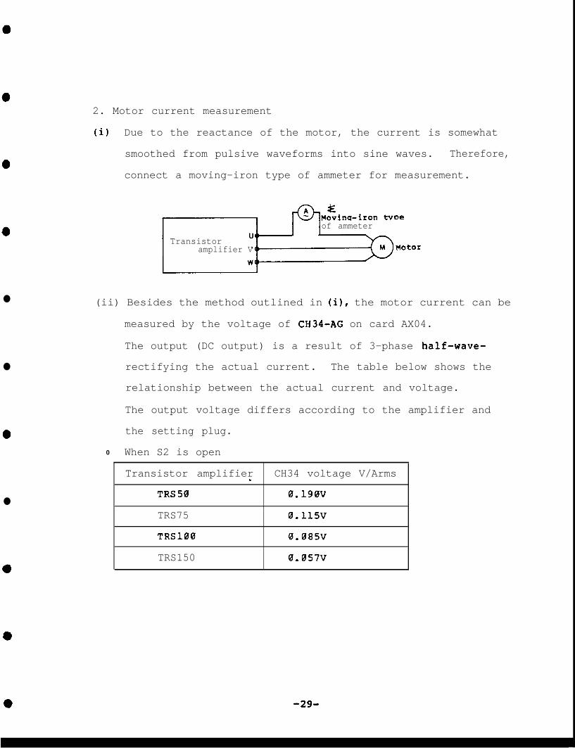
2. Motor current measurement
l
l
l
(i) Due to the reactance of the motor, the current is somewhat
smoothed from pulsive waveforms into sine waves. Therefore,
connect a moving-iron type of ammeter for measurement.
of ammeter
Transistoramplifier V
(ii) Besides the method outlined in (i), the motor current can be
measured by the voltage of CH34-AG on card AX04.
The output (DC output) is a result of 3-phase half-wave-
rectifying the actual current. The table below shows the
relationship between the actual current and voltage.
The output voltage differs according to the amplifier and
the setting plug.
0 When S2 is open
Transistor amplifier CH34 voltage V/Arms.
TRS50 0.190V
TRS75 0.115V
TRSl00 0.085V
TRS150 0.057V

0 When S2 is shorted
Transistor amplifiel Setting CH34 voltage V/Armsplug s3
TRS50 0 0.060U
0.024U
TRS75 0.015U
TRSl00 0.01lU
TRSl50 0.0072V
o denotes shorted.
0
l
l
l
l
l

l
l
l
2) TRANSISTOR AMPLIFIER INSPECTION
a) Operating display lamps
DBL
0‘clCRAB)
OLED524V
Lamp
RDY (RAl)
Function
For checking NC READY status
SVON (RA2) For checking whether servo is
ON or OFF.
DBL (RAB) For checking dynamic brake
operation.
24V (LEDS) Lights when start signal is
is issued from NC system.
b) Alarm displays
ALARM
0 LED 1
LED2
LED3
LED4
LED
Lights with READY ON.
Lights with servo ON.
Lights when brake is
OFF.
Lights when power is
ON.
LED lights
l
l -31-

The alarms are detailed below:
Instantaneous power failure compensation/under-voltage
compensation (LVAL)
The circuitry is protected when the supply voltage is
instantaneously cut off or when the voltage drops to an
abnormally low level.
Instantaneous overcurrent detection (OCP)
The transistors are protected when an overcurrent
momentarily flows to the transistors in the circuitry.
Overcurrent detection (OVC)
This protection circuit functions when an overcurrent has
flowed to main circuitry for more than a fixed period of
time.
Overspeed (TGOV)
The motor is protected when the motor speed exceeds its
rating due to a malfunction.
No-signal detection (NSG)
This alarm functions when the signals are no longer fed back
from the resolver to the transistor amplifier. (This is for
detecting the magnetic pole position.)
-32-
0
l
l
l
l

l
l
0
l
l
l
l
0
l
6 Power unit alarm (PUAL)
Power unit alarm display.
Refer to the section on INSPECTION OF POWER UNIT for further
details of the alarm.
7 Fin overheating (F.OH)
Protection is provided when an overcurrent flows to the
circuitry and the fin mounted on transistors overheats.
8 Motor overload (M.OH)
Protection is provided when motor is overloaded and it
overheats.
c) REMEDIES FOR ALARMS
1) LVAL
(1) Measure the AC 100V voltage of the amplifier terminal block
using a multimeter or synchroscope. Rating: 8%110V.
(2) When there is nothing unusual with the voltage, the trouble
may be an instantaneous power failure. Check the AC 100V
and AC 200V wiring connections.
2) OCP
(1) Check using a multimeter whether the power transistors have
been damaged. Disconnect the wires and measure across the
collector and emitter of the transistors. When nothing is
wrong, the resistance is at infinity.
0 -33-

(2) Check whether the connections inside the amplifier have been
made improperly and whether any screws are loose.
3) ovc
(1) Check whether a higher current than the rating is flowing to
the motor.
(2) Check that the AX04 card settings have been made properly.
4) TGOV
(1) Check that the AX04 card settings have been made properly.
(2) Check that the TG voltage is 0V while the motor has stopped.
5) NSG
(1) Use a synchroscope to measure whether the resolver feedback
voltage is 12V.
l
0
l
l
(2) When the voltage is BV, check the cables and connectors.
(3) When the voltage is lower, useVRl0 to adjusttheCH16
voltage to 12Vp-p.
6) PUAL
(1) Check out the power unit.
(2) Refer to page 36 for the alarm displays
7) FOH
(1) Check that none
been damaged.
of the amplifier's power transistors have
l
l
a
e
0
-34-*

(2) Check if any units other than the power transistors are
generating heat.
8) MOH
(1) Check whether the motor is generating heat
armature current. If the current is high,
proper motor has been selected.
(2) If the motor is not hot, disconnect Gland
fier's terminal
power is still
the resistance
block and use a multimeter to check whether
and measure the
check whether the
G2 on the ampli-
flowing or not. When everything is in order,
is zero.
0 -35-

3) POWER UNIT INSPECTION
1) Power onit operation status displays and alarm display lamps
(TR115A control card)
Name Lamp Description of display
)P- Pi lot PLll Lights when DC voltage of rectifier unit is
srat- approx. 80V; off w h e n approx . 40-50V.
Do NOT touch since capacitor is still charged
PW. ON LED1 Lights when +24V is supplied by DUC-1 cable
(green) (ZP12 connector) from transistor amplifier.
Al- THM LED2 Lights when temperature of rectifier diode
arm (red) exceeds prescribed temperature.
sta- Alarm for all axes.
tus NFB LED3 Lights when no-fuse breaker of rectifier
(red) unit is tripped or when it goes OFF.
Alarm for all axes.
ALM LED4 When multi-tap transformer or RU unit isinstalled, the RU unit will be an alarm or
(red) when transformer thermal is operated thiswill be an alarm. Alarm for all axes.
FUSE LED5 Lights when the AClOOV fuse or the fuse in thepower unit output (P) breaks. Alarm for all
(red) axes.
1
.J
- 36 -
*
l
l

2) Description of power unit check pins
Check pin Signal Description of signal
CPl +24V DC +24V is output at same time as +24V is
supplied from NC system to amplifier. At
this time, LED1 (green) lights.
CP2 RG CPl-CP4 ground
CP3 AL Low-level signal (normally* open) when alarm
occurs inside power unit. At this time, one
of the lamps from LED2 to LED5 will light.
CP4 CR Signal which observes time constant of soft-
start circuit. Activates contactor sequence.
l
0
0 -37-

3) Power unit card
_ __ _ _ _ __ __ _ 0
1 ZPll !2 loI
CPI 2 a 4
- 0
N 0
c
- 0
0000 0w2 w 3 w4 LED5 WlTHM NFB AL!4 FUSE AN-ON
Control card (TR-115)l
l
-38-

4) POSITION LOOP OFFSET AND DROOP ADJUSTMENTSl
Item Adjustment Remarks
Dffset 1 Display screen 5 with ALARM/DIAGNOSIS
adjust- control at NC side..; (With MQ)
aent 2 Check that NC READY signal appears.
3 Adjust VR7 on AC transistor ampli-
fier and set POSITION DROOP to +/-2.
Droop 1 Display screen 5 with ALARM/DIAGNOSIS
adjust- control at NC side.
ment 2 Check that detector being used and
name of detector on screen tally.
3 Check that TAU and LINEAR ZONE are
correct.
4 Calculate position droop from formula
below: Feedrate (mm/min) x 1 x 260 gain
Feedrate is Fl000 (approx. 100 rpm
motor speed)
5 Feed axis 1 so that position droop is Remember that
made (+) and use VR2 on AC transistor this differs
amplifier to adjust to position droop from machine's
in (4). (+)(-I direc-
tions.

Item I Adjustment Pemarks6 Feed other axes so that position droo
is made (+) and adjust to within +/-1%
of droop adjusted in (51.. s
a
l

l4) POSITION LOOP OFFSET AND DROOP ADJUSTMENTS
Item Adjustment Remarks
Offset 1 Display screen 5 with ALARM/DIAGNOSIS
adjust- c.ontrol at NC side..? (With MQ)
ment 2 Check that NC READY signal appears.
3 Adjust VR7 on AC transistor ampli-
fier and set POSITION DROOP to +/-2.
Droop 1 Display screen 5 with ALARM/DIAGNOSIS
adjust- control at NC side.--;_ .: nent 2 Check that detector being used and
l name of detector on screen tally.
3 Check that TAU and LINEAR ZONE are
correct.
l 4 Calculate position droop from formula
below: Feedrate (mm/min) x 1 x 260 gain
Feedrate is Fl000 (approx. 100 rpm
motor speed)
0
5 Feed axis 1 so that position droop is Remember that
made (+I and use VR2 on AC transistor this differs
amplifier to adjust to position droop from machine's
in (4). (+I (-1 direc-
tions.
‘.
0 -390

,
Item Adjustment Remarks
6 Feed other axes so that position droop
is made (+) and adjust to within +/-1%
of droop adjusted in (S),.
0
l
--.,
0
l

0
l
5) RESOLVER FEEDBACK ADJUSTMENT
Item Adjustment Remarks
Feed- 1 Measure check pin TPl on GX96 card
back using synchroscope. (M-LB, MB) PIvoltage 2 Voltage should range from 8Vp-p to *=
p3I
check 13vp-p. Short-circuit S5 if higher%I
00
than 13Vp-p.
Ampli- 1 Obtain highest and lowest points of
tude waveform at check pin TPl, set volt-
fluctua- age range to 0.2V/DIV and set time
tion base to 0.1-0.2 sec/DIV. c'*?Iadjust- 2 Drive machine at 3-4 m/min and ad- e
ment just VRl and VR2 so that amplitude
fluctuation is made less than 40
mVp-p.
(GX96 card) ~llrllrrlllrllrlrllllllllllJ~J~~
3 To set voltage range to Q.ZV/DIV, use
synchroscope ADD and shift with both
channels 1 and 2.
-41-

6) MOUNTING THE DETECTOR
The motor's magnetic pole position (magnet position) must be
detected in the AC servo system. Therefore, the detector is
mounted differently from that in a DC servo system. The method. . 3. &':'
is shown below.
1) Detector mounting surface
Fig. 1 Motor detector mounting surface
4-n5 x Q.R, 7.S rleothMark-off 1 ine I /
Rev
2) Detector(With bellows)
Fig. 2 Detector (with bellows)
Positionins marks
Rlonqated hole
c$ Key groove
O-ring S75installation ",fkF'"'----__-
3) Installation (when sensor is installed indirection A)
-Y ’SensorHA m o t o r Note
When the sensor is Installed in directions B, C or D,the sensor connector moves accordingly to positions B,C or D as shown in the above diagram.
-42-

l
0
0
4) Installation method(1) Install the O-ring (S75) to the
sensor flange.(2) Install an M4 hexagonal bolt with
hole to the coupling.(3) Align the motor shaft key with key
groove in the sensor bellows(4) Align the sensor positioning mark
with the motor mark off line.(5) Install the sensor to the motor
(using M5xO.8 screws).(6) Tighten the screw on the key groove
to secure the key so that it cannotmove.
(7) Insert the sensor rubber plug
Note: The bellows should not be detached from the detector
since the positions ofthesetwoparts standin a precise
relationship.
0-43-