Construction and commissioning of a three-phase four-leg ...
104
UNIVERSITA’ DEGLI STUDI DI PADOVA Dipartimento di Ingegneria Industriale DII Corso di Laurea Magistrale in Ingegneria dell’Energia Elettrica Construction and commissioning of a three-phase four-leg grid-forming inverter. Relatore: Prof. Nicola Bianchi Correlatore: Prof. Fernando Briz Del Blanco Carlo Piccoli, 1157146 Anno Accademico 2018/2019
Transcript of Construction and commissioning of a three-phase four-leg ...

UNIVERSITA’ DEGLI STUDI DI PADOVA
Dipartimento di Ingegneria Industriale DII
Corso di Laurea Magistrale in Ingegneria dell’Energia Elettrica
Construction and commissioning of a
three-phase four-leg grid-forming inverter.
Relatore: Prof. Nicola Bianchi
Correlatore: Prof. Fernando Briz Del Blanco
Carlo Piccoli, 1157146
Anno Accademico 2018/2019

2

3
A Pierina e Giovanni.

4

5
Summary
Introduction ............................................................................................................................................ 9 0.1 - Motivations ................................................................................................................................ 9 0.2 - Two levels inverter .................................................................................................................... 9
0.2.1 – Inverter’s topology: 3P4L ................................................................................................ 10 0.3 - Grid connected inverters .......................................................................................................... 10
0.3.1 – Modes of operation: grid feeding and grid forming ......................................................... 10 0.4 - Structure of the control: cascade control .................................................................................. 12 0.5 – Target, methodologies and contents’ organization .................................................................. 12
Chapter 1: Hardware structure ............................................................................................................. 15 1.1 – Inverter .................................................................................................................................... 15
A.1.1 - Electrical structure ........................................................................................................... 16 A.1.2 - Thermo-mechanical structure ........................................................................................... 17
1.2 – DSP electronic board ............................................................................................................... 17 1.2.1 - Digital signal controller (DSC) ......................................................................................... 19 1.2.2 – Components and their application .................................................................................... 19
1.3 – Peripheral equipment ............................................................................................................... 23 1.3.1 – Power supplies.................................................................................................................. 23 1.3.2 – Current and voltage sensors ............................................................................................. 23 1.3.3 – External voltmeter ............................................................................................................ 24 1.3.4 – Charging and discharging resistors .................................................................................. 26 1.3.5 – Fuses ................................................................................................................................. 27 1.3.6 – Circuit breakers and contactors ........................................................................................ 28
1.4 – Cabinet organization and cabling ............................................................................................ 29 1.4.1 – Cabinet’s component organization; inside and outside .................................................... 29 1.4.2 – Cabling: design and characteristics .................................................................................. 32 1.4.3 – Cabling: standard installations ......................................................................................... 34 1.4.4 – Cabling: ad hoc installations ............................................................................................ 35
Chapter 2: Modulation ......................................................................................................................... 37 2.1 - Pulse Width Modulation (PWM): sine-triangular technique.................................................... 37
2.1.1 - General principles of Pulse Width Modulation; sine-triangle technique .......................... 37 2.1.2 - PWM management in three phases inverter to feed a three phases load ........................... 40
2.2 - Homopolar injection in sine-triangular PWM .......................................................................... 42 2.3 - PWM implementation with TMS320F28335 ........................................................................... 45
2.3.1 - TMS320F28335 ePWM module features ......................................................................... 45 2.3.2 - TMS320F28335 ADC module features ............................................................................ 47
2.4 - PWM signal actual programming ............................................................................................ 48

6
2.4.1 - TMS320F28335 ePWM module initializing ..................................................................... 48 2.4.2 - TMS320F28335 ADC module initializing ........................................................................ 50
2.5 - Tests to check PWM driving signal and generated voltage ..................................................... 51 2.5.1 - PWM driving signal test ................................................................................................... 51 2.5.2 - PWM generated line to line voltage test; full bridge configuration. ................................. 53 2.5.3 - PWM generated three phases voltage test ......................................................................... 54
Chapter 3: Current Control (CC) .......................................................................................................... 57 3.1 – CC implementation ................................................................................................................. 57
3.1.1 – Scheme for continuous time analysis ............................................................................... 58 3.1.2 – Scheme for discretized time analysis ............................................................................... 60
3.2 – CC simulations, tests and improvements ................................................................................. 62 3.2.1 - Realizable references anti-windup technique: implementation ......................................... 62 3.2.2 – Continuous reference CC: null theta ................................................................................ 63 3.2.3 – Rotating reference CC with realizable references ............................................................ 65
Chapter 4: Voltage Control (VC) ......................................................................................................... 67 4.1 – VC implementation ................................................................................................................. 67
4.1.1 – Cascade control ................................................................................................................ 67 4.1.2 – Grid filter basic design ..................................................................................................... 68 4.1.3 – Feed forward .................................................................................................................... 70 4.1.4 – Pre-filter (PF) ................................................................................................................... 71 4.1.5 – Pre-filter discretization ..................................................................................................... 71 4.1.6 – Final VC and CC cascade control structure ...................................................................... 72
4.2 – VC simulations and tests ......................................................................................................... 73 4.2.1 – Tests settings introduction ................................................................................................ 73 4.2.2 – Continuous reference VC: null theta ................................................................................ 76 4.2.3 – Rotating reference VC ...................................................................................................... 80
Chapter 5: Conclusion and contributions ............................................................................................. 85 Chapter 6: Future developments .......................................................................................................... 87
6.0.1 – Filter’s improvement ........................................................................................................ 87 6.0.2 – Study of a 3P4L-VSI dynamic strategy management....................................................... 87
Bibliography ......................................................................................................................................... 91 Appendix A: Hardware’s components reference table ......................................................................... 93 Appendix B: Codes .............................................................................................................................. 95
B.1 – Main.C .................................................................................................................................... 95 B.2 – Microprocessor settings .......................................................................................................... 99 B.3 – Functions .............................................................................................................................. 103

7
Abstract
Because of the existing trend in renewable energy integration, the concept of a completely inverter-based power system is becoming more and more realistic.
This work presents a method for managing grid-forming inverter in an islanded AC microgrid, which is operated at constant frequency, and a hardware implementation of the system which the author himself built and tested.
The control solution is based on a cascade current and voltage control with PI regulators.
The hardware components that refer to it are many: a TI’s DSP, optical fibres communication system, Hall’s effect sensors for voltage and current measurements, analogic to digital channels to convert and filter the measurement signal and others.
It is also presented a technical solution for the DC-bus charging and discharging circuit.
A simplified LC grid-filter design is exposed.
It is presented a possible implementation of the user interface located on the door of the cabinet.
Furthermore, the performances of the built cabinet are then compared with a MATLAB Simulink model of the whole microgrid.
(Italian version)
In ragione dell’attuale tendenza all’integrazione delle energie rinnovabili nel portafoglio energetico di molti paesi, l’idea di un sistema elettrico basato totalmente su sistemi di conversione statica è sempre più realistica. Il seguente lavoro presenta un metodo per la gestione di un inverter per grid-forming, in una micro-rete AC isolata ed esercita a frequenza costante, e una implementazione del Sistema micro-rete-inverter che l’autore ha personalmente costruito e testato. La soluzione per il controllo si basa su un controllo a cascata di corrente e tensione tramite regolatori PI. La componentistica afferente al sistema di controllo va dal microprocessore della TI al sistema di comunicazione tramite fibra ottica, alle sonde ad effetto Hall per le misure di correnti e tensioni, ai canali per la conversione da analogico a digitale dei segnali di misura e il loro filtraggio, etc. Sono presentate soluzioni impiantistiche per i circuiti di carica e scarica dei condensatori del bus in continua, un progetto semplificato del filtro di rete di tipo LC e una possibile struttura dell’interfaccia per l’utente situata sulla portiera dell’armadio. Per concludere, i risultati dei test del sistema per grid-forming sono stati confrontati con un accurato modello costruito con MATLAB Simulink.
(Spanish version)
Debido a la tendencia a la integracion de las energias renovables en las redes electricas, la idea de un sistema basado por completo en una alimentaccion procedente de convertidores de potencia se está haciendo más realista. Este trabajo presenta un metodo para gestionar un inversor para formación de red en una microred aislada en AC con frequencia constante y una implementación del sistema microred-inversor que el mismo autor construyó y comprobó. La soución propuesta para el control se basa en un control en cascada de corriente y tensión por reguladores PI. Los componentes usados en este sistema de control son variados: un microprocessador de TI, 12 canales de fibra optica, sensores de efecto Hall para medir corrientes y tensiones, canales para la conversion de analogico a digital de las señales y para filtrarlos, etc. Se presenta un diseñpara la instalacion de los circuitos de carga y de descarga del DC-bus, un diseño simplificado del filtro de red (tipologia LC) y una possible instalacion de la interfaz del usuario ubicada en la puerta del armario electrico. Por ultimo los datos recogidos durante las pruebas estan comparados con los de las simulaciones hechas por MATLAB Simulink con un modelo de todo el sistema de grid-forming.

8

9
Introduction
0.1 - Motivations Pollution and climate changes are two of the many reasons that are leading the world to find innovative energy sources that must be emission free and renewable. Then, efficiency and waste reduction in energy field are going to become not only an economic goal but also an environmental requirement. For these reasons, traditional energy production, mainly based on fossil combustion (oil, gas, carbon), must be converted and/or improved.
Many innovations are changing the current energy systems; in particular, the Distributed Energy Resources (DER), such as most of renewable sources (PV plants and wind turbines in first place), modify the traditional electric grid structure, reducing distinction between production sites and consumption areas.
Progress in power electronics provides new devices able to exchange huge amounts of power in time ranges unfeasible for traditional electrical machines, decoupling sources and loads. For many of these reasons microgrids [1] and a strong use of power electronics converters called voltage source converters (VSC) instead of synchronous generators [2] [3] are becoming more and more an interesting electric conformation.
This text presents a method for managing grid-forming inverter in an islanded AC microgrid, which is operated at constant frequency, and a hardware implementation of the system which the author himself built and tested.
0.2 - Two levels inverter A very big variety of inverter types exists but in this work the whole multi-level type will be neglected to focus on the two levels type.
Let’s consider the very basic three-phase three-leg electrical structure, a LC grid filter and a balanced microgrid connected to it.
DC link
LfTHREE-PHASE
BALANCED LOADA
B
C
Cf
Introduction, Figure 1 – 3F3L grid-forming inverter with grid filter and its microgrid: a three-phase balanced purely resistive load.

10
It behaves very properly when the load is balanced but it can be upgraded with the purpose of facing unbalanced three phases loads.
0.2.1 – Inverter’s topology: 3P4L Let’s now consider the three-phase four-leg electrical structure and a simple microgrid connected to it.
DC link
LfTHREE-PHSE
UNBALANCED LOADA
B
C
N
Cf
Ln
Introduction, Figure 2- 3F4L grid-forming inverter with grid filter and its microgrid: a three-phase unbalanced purely resistive load.
What’s peculiar of this circuit structure is the capability to manage unbalanced load and fault conditions better than the 3P3L thanks to its fourth leg.
In [4], it is possible to see the ability of this inverter type to overcome the challenge of feeding unbalanced, non-linear and continuously changed load with balanced three-phase voltages.
0.3 - Grid connected inverters Because of the existing trend in renewable energy integration, electrical power systems are nowadays facing a great transition from large Synchronous Machines (SMs) to smaller generation units, interfaced via Voltage Source Converters (VSCs).
The presence of existing SMs still allows for the greatest part of inverter-based generation to be controlled as grid-feeding units. Nevertheless, this mode of operation depends on the assumption of a strong AC grid and accurate tracking of the already formed frequency and voltage but this assumption collapses in the case of systems with 100% Power Electronics (PE) penetration. [3] Then, several grid-forming control strategies have been proposed too.
0.3.1 – Modes of operation: grid feeding and grid forming Depending on their operation in an ac microgrid, according to the literature [5], power converters can be classified into three main categories: grid-feeding, grid-supporting, and grid-forming power converters. In these lines the grid-supporting category will be neglected.
First of all, the grid-forming power converters can be basically represented as ideal AC voltage sources with low-output impedance, in which the voltage amplitude E_ref and frequency f of the local grid are set by using a proper control loop. [6] The following figure describes such a system.

11
Cv
Z
V*
f
E_ref
AC micro-gridbus
Introduction, Figure 3 – Simplified representation of a grid connected power converter system: grid forming.
A classical controller configuration for a grid-forming power converter is made by using two cascaded synchronous controllers working on the dq reference frame. The inputs to the control system are the amplitude E_ref and the frequency f of the voltage. The external loop controls the grid voltage to match its reference value, while the internal control loop regulates the current supplied by the converter (such a control scheme will be deeply studied in this thesis work). Therefore, the controlled current flowing though the grid filter’s inductor charges the grid filter’s capacitor to keep the output voltage close to the reference provided by the voltage control loop. Usually, in industrial applications, these power converters are fed by stable dc voltage sources driven by any kind of primary source.
On the other hand, the grid-feeding power converters are mainly designed to supply power to an already existing grid whose main energization comes from another source. They can be represented as ideal current sources connected to the grid in parallel with high impedance. A simplified scheme of the grid-feeding power converters is shown in the following figure, where P_ref and Q_ref represent the active and the reactive powers that have to be delivered by the static conversion power machine. [6] What’s here fundamental it the fact that the current source must be perfectly synchronized with the ac voltage at the connection point, with the purpose of accurately regulating the active and reactive power exchanged with the grid.
CiI*
P_ref
Q_ref
AC micro-gridbus
Z
Introduction, Figure 4 - Simplified representation of a grid connected power converter system: grid feeding.

12
These converters can participate in the control of the microgrid AC voltage amplitude and frequency by adjusting the references of active and reactive powers, P_ref and Q_ref, that have to be delivered.
A big and unforgettable difference between the two types is that in a microgrid, the AC voltage generated by the grid-forming power converter will be used as a reference for the rest of grid-feeding power converters connected to it while a grid-feeding power converter could not be used in such a way. This because the first power converter type can withstand the islanded-mode [7] while the grid following ones can’t.
0.4 - Structure of the control: cascade control As stated in the previous paragraph, a grid forming system can be managed thanks to a cascade control; let’s introduce this concept.
It is a kind of many levels control system with an inner loop, which is times faster than the outer one, that allows to manage the control of many signals. Here a figure of a general cascade control with two levels where:
d1 and d2 are two disturbances the scheme shows two feedback controls it is assumed that the two regulators are of PID typology.
Introduction, Figure 5 - Blocks representation of a general cascade control.
In cascade control there are two PID regulators arranged with one PID controlling the setpoint of another. A PID controller acts as outer loop controller while the other acts as inner loop controller, which reads the output of outer loop controller as setpoint. Usually the configuration expects an inner loop ten times faster than the outer loop as minimum.
Basically, through a cascade control it is possible to delete the effects of the inner disturbance d1 in such a little time that the outer controller can neglect such a disturbance.
To reach this goal the inner loop is usually built with high gains or it can even be controlled with a proportional controller; then it is possible to build the outer control loop controller with the desired bandwidth.
0.5 – Target, methodologies and contents’ organization With the purpose of dispose of a 3P4L grid-forming inverter which could handle a test-grid for the research laboratory, during the design, the construction and the tests, the analysis had got two main targets:

13
A working technical solution for the whole inverter and microgrid system’s structure including: a 3P4L inverter, a DC-bus charging circuit, a LC grid filter, a complete current and voltage measurement system and an external user interface.
To verify that the tests, while a grid is formed, fit with the theoretical results exposed in the literature and get by the simulation tests.
Then, the following methodologies/steps were chosen at the beginning of the work:
1. To design the cabinet as suggested in the seller components’ datasheet, in the literature and, above all watching the other cabinet of the laboratory.
2. To build a model of the whole micro-grid system (cabinet and three-phase balanced load) in MATLAB Simulink.
3. Comparison between model’s simulation results and the theoretical behaviour of such a model, in order to check the good quality of the model.
4. To check if experimental results and model results match with the purpose of verifying the hardware and that the control works properly.
As it possible to imagine such a methodology is particularly based on trial and error because a hardware implementation is always much more complex than what is possible to design and this is also true for a control implementation. For this reason, the text won’t report all this long trial and error process.
It will be divided in 4 chapters. The first deals with cabinet’s hardware structure and components (except the Texas Instruments’ microprocessor which is deeply described in chapter number 2). The second is focused on how the PWM signal is produced and it contains many tests that show the proper behaviour of the IGBTs of the inverter. In the following chapter current control loop is introduced. These pages deal also with the grid-forming system’s MATLAB Simulink structure and show the behaviour of the inverter’s current managed with such a control. The fourth focuses on the whole voltage and current cascade control and shows some improvements of the control shown in Chapter 3. It finishes with the comparison between experimental results and model results.
At the end, after conclusions and future developments, it is possible to find two appendixes; Appendix A reports a list of all components’ datasheet while in Appendix B the main body of microprocessor’s programming code is shown.

14

15
Chapter 1: Hardware structure
Since the very beginning of this work it was necessary to dedicate a lot of time (approximately 3-4 months over the 7 months of the project) to the hardware construction. The main body of the inverter was already built so the efforts were focused on testing and organizing the cabinet system and the printed circuit board (PCB) that commands the inverter and manages all the measurement equipment into the cabinet.
In order to show in detail the structure of the whole system, it seems useful dividing this description/picture in 4 parts; the first deals with the inverter, the second about the PCB, in third place a description of each component used in the cabinet and at the end a scheme which represents the real 3 phases 4 legs inverter’s cabinet.
For the purpose of an easy consultation, all the components references are indicated in the table of Appendix 1.
Chapter 1, Figure 1 - Picture of the final structure of the cabinet and connections.
1.1 – Inverter Here below the description of the inverter is developed distinguishing between what concern to the electrical scheme and what concern the thermo-mechanical structure.

16
Chapter 1, Figure 2 - The picture of the whole 3P4L inverter completely mounted.
A.1.1 - Electrical structure The inverter is the heart of the cabinet and, in first place, it’s composed by four power modules containing two insulated gate bipolar transistors (IGBT) each; on their top are located four dual IGBT driver boards which are responsible of controlling their own switches. As the modules as the drivers are made by Infineon.
Chapter 1, Figure 3 - The driver by Infineon in located on the top of the electronic board on which it is possible to recognize: 3 optical fibre gates, the fault led, the blue 6 pins terminal (sending errors to the DSP), the white power feeding terminal, 2 feeding checking led and the button to reset the error signal. The white plastic object
with 4 bolts, that lies under the driver, is the power module.
In second place there is the DC bus, formed by five capacitors of 500 µF connected thanks three copper plates: the lowest is the positive pole of the bus, the middle one is the negative pole and the highest is the half voltage point. The peculiar connection between the capacitors is shown here.

17
500 μF 500 μF 500 μF
500 μF
500 μF
Positive
Negative
Half voltage
Chapter 1, Figure 4 - On the left the electrical connections of the DC-bus where have been underlined with big dots the points where is possible to put a measurement and/or feeding terminal; on the other side there are two of
the five capacitance. Is possible to notice that they are connected to the DC-bus copper plate through screws whose diameter is 6 mm.
A simple calculation can show that the final capacitance of the inverter is 1725 µF.
A.1.2 - Thermo-mechanical structure There are 4 fans to dissipate the heat produced by losses in the IGBT; they are divided in two couples, each of them connected with two power modules.
A metallic skeleton sustains each of the fan and all the electrical components together. It is made with an aluminium plate, in which are locked the capacitors, and with some X-shaped beams that connect mechanically the DC bus with the rest of the electrical components.
Chapter 1, Figure 5 - The picture shows as the fans as the mechanical structure and how those two are integrated with the electrical system.
1.2 – DSP electronic board This piece was designed by Escuela Politecnica de Gijon not only for the 3P4L inverter but for many other applications. For this reason, the main goal of the section is to describe only the specific constituents used in this project and their targets, without going into the other components.

18
Chapter 1, Figure 6 - The complete electronic board used in the project.

19
1.2.1 - Digital signal controller (DSC) It is the main core of the electronic board; it’s produced by Texas Instruments and has a high performance 32 bits digital signal processor (DSP). To have a synthetic overview of this component’s features there is the following table.
FEATURES
Up to 150 MHz (6.67 ns Cycle Time)
Feeding voltage of 3.3 V I/O Design
Up to 88 shared general purpose input/output (GPIO) pins
Watchdog timer
Up to 18 PWM outputs
12-bit ADC, 16 channels 80 ns conversion rate – 2 × 8 channel input multiplexer
– two sample-and-hold – single/simultaneous conversions
– internal or external reference Chapter 1, Table 1 - TMS320F28335 features synthetic overview.
Chapter 1, Figure 7 - TMS320F28335.
1.2.2 – Components and their application As is possible to see in the first picture of this paragraph A.2, over the board are spread many components but it is useful to recognize that each zone is dedicated to a peculiar function: the top is used to get the voltage supplies and the input signals coming from the external current and voltage sensors, in the centre there are 16 rectangles that can be used to locate the analogic to digital signal converters (ADC), at its right there is the DSC and at the top right there is a column of optical fibres fed by six supply voltage devices directly driven by the DSC. There are two more zones: the fifth is at the bottom in the right and here there is a little board used to connect the DSP with the pc while the sixth, which includes all the left components in the bottom and it is dedicated to the error signal input system; it consists on a simple logic error check which is basically composed of three level: in the lowest, each of the four optical fibre input doors communicate directly with one of the four devices (dual 4-input positive -and gate) that, in case of error, send a signal to the upper level device1 that can receive the error information from any of the lower level device and transmit it to the final device2 which disables the PWM fibres signals. These last two zones will be neglected because even if they are mounted, they have not been used in any experimental test.
1 This is made by one or more logical elements. They are called SN74LS07.
2 It is called CMOS quad 3-state R/S latch

20
Chapter 1, Figure 8 - In order from first to sixth: green (voltage supplies), orange (ADCs), red (DSC), blue (optical fibre outputs), yellow (error signal receiving system) and light blue (debug).
In the first zone the voltage supply component receives 4 signals: 5 V, GND, +15 V and -15 V which are filtered, to avoid ripple, by 3 capacitors of 1000 µF each. Under the orange element situated in the left side of the top, used to receive the input signals from the sensors, it is located the step-down voltage regulator(TL082). In the implementation scheme it is possible to recognise the capacitors that avoid the ripple of the voltage supply of the logic component, the Zener diode which protects the DSP in case of too high voltage (> 3.3 V) and the resistance R44 which decreases the current flowing into the input terminal.
Chapter 1, Figure 9 - Step down voltage (from 5 to 3 V) electrical implementation scheme.

21
In the second zone are contained the ADC blocks that consist of the dual operational amplifier, the capacitors C3 and C4 of 100 nF that maintain constant the feeding voltage, the measurement resistance 𝑅𝑚1, the gains resistances and a filter of 4.25 KHz to reduce the digital signal ripple.
If in one hand the first operational scheme is easy to understand because is characterized by a gain of 𝑅2 𝑅1⁄ and inverts the signal sign, in the other hand there is an active low-pass filter with a multi-feedback configuration which inverts the signal sign and whose transfer function is:
𝐺(𝑗𝜔) =−𝑅6 𝑅4⁄
1 + (𝑅5 ∙ 𝐶2 + 𝑅6 ∙ 𝐶2 +𝑅5 ∙ 𝑅6 ∙ 𝐶2
𝑅4) (𝑗𝜔) + 𝑅6 ∙ 𝑅5 ∙ 𝐶2 ∙ 𝐶1 ∙ (𝑗𝜔)2
[4]
From which it is possible to recognize that filter’s gain is equal to 𝑅6 𝑅4⁄ while filter’s cut-off frequency is:
𝑓𝑐 =1
2𝜋 ∙ √𝑅6 ∙ 𝑅5 ∙ 𝐶2 ∙ 𝐶1
Here below is reported the whole ADC channels electrical scheme divided in two to make the figures clearer.
Chapter 1, Figure 10 - Left half of the ADC channel electrical implementation scheme.
Chapter 1, Figure 11 - Right half of the ADC channel electrical implementation scheme.

22
The following table is a summary of the most remarkable data of the ADC channel used to measure one phase current.
COMPONENT VALUE ELEMENT MAIN CHARACTERISTIC
Rm1 R1 2 kΩ R2 1 kΩ C3 100 nF C4 100 nF
TL082 A 𝐺𝑎𝑖𝑛𝐴 = 1 2⁄ R4 3 kΩ R5 1.74 kΩ R6 3 kΩ R7 55 Ω C1 27 nF C2 10 nF
D1 (Zener diode) 3 V TL082 B 𝐺𝑎𝑖𝑛𝐵 = 1
Chapter 1, Table 2 – ADC channels’ data.
Neglecting the DSC, whose behaviour is completely described in its datasheet, here the text deals with the optical signal fibres system. This equipment is used to link the DSP with each module’s driver and the connection scheme is represented here. These connections3 send to the IGBTs’ drivers the switching-time signals the power modules have to respect due to produce the voltage wave that the PI regulator asks for.
Chapter 1, Figure 12 - Optical fibre electrical implementation scheme. What’s important to recognize is that the optical fibre inverts the signal.
There are 4 couples of optical fibre signals, one for each leg of the inverter, and 4 more signals used to enable driver transmission of the PWM signals to the correspondent IGBT. Each fibre gate is preceded by a 100 nF capacitor and two resistances used to stabilize the optical fibre voltage and current supply.
3 It is very useful underline once more that the logic fibres invert the signal coming from the DSP.

23
1.3 – Peripheral equipment With this name are indicated all those systems that are essential for the complete cabinet operation but that are not essential to make the inverter working properly.
First of all, the power supply devices then the current and voltage sensors which are required to implement the current control loop and the voltage control loop, in third place the description of the external voltmeter and its electronic boards and finally the two group of resistors used to charge and discharge the DC bus.
1.3.1 – Power supplies The whole cabinet requires many secondary systems: heat dissipation system, protection system, data collecting system and others. There are 2 power supplies for the purpose of feeding all these secondary systems; one manages the 5 and ±15 V systems and the other the 24 V systems. Here below it is shown how is the whole feeding system structured.
24 V Distribution Electronic
BoardDriver 1 Driver 2 Driver 3 Driver 4 Fan 1 Fan 2 Fan 3 Fan 4
24 V
GND
24 VPower Supply
L N
GND 24 V
Chapter 1, Figure 13 - 24 V devices feeding scheme.
5, ±15 VPower Supply
5 V
GND
Voltmeter Display
Electronic Board
DSP Electronic Board
Current Sensor 1 (CS1) CS2 CS3 CS4 DC-bus
Voltage SensorPhase Voltage Sensors
Electronic Board
+15 V
-15 V
L N
Chapter 1, Figure 14 – 5, ±15 V devices feeding scheme.
1.3.2 – Current and voltage sensors In order to analyse and to control the four phases’ currents and voltages the cabinet possesses one current sensor for each leg and an equal number of voltage sensors: one of them measure the DC bus voltage and the other three dedicate to phase a, b and c. It will be possible to notice that all these sensors are

24
sized to measure quantities bigger than those read on the previous chapters; this is not the effect of wrong dimensioning but a choice made at the beginning of the project: as well as avoiding critical working condition, this choice will allow future power development of the 3P4L inverter.
The current sensors are 4 identical pieces; they can handle current of big size, 1000 A as nominal current, and can work thanks to the Hall effect. They actually are current transducers with a galvanic isolation between the primary circuit (power side) and the secondary (electronic side); so, with this architecture, the current sensor reach a current ratio of 1:5000 and a secondary nominal current of 200 mA. It is useful to underline that to achieve the aims, analysis and control, this equipment provides the following advantages: wide frequency band width, little linearity error and high immunity to external interferences, which are necessary to have a precise and dynamic control.
Chapter 1, Figure 15 - From left to right: current sensor, DC-bus voltage sensor, electronic board with three voltage sensors.
The voltage sensor that handles of measuring the DC bus potential difference has a nominal voltage of 1000 V but can reach 1500 V as maximum. In this case also, the equipment is a transducer with an isolation barrier between primary circuit and secondary and it has a conversion ratio of 0.05 A going out of the secondary each 1000 V going into the primary. Like the sensors seen above this one presents many advantages but, in our application, the main relevant is: low linearity and sensitivity error.
It can be seen from the picture that to get an accurate measurement of the three phases’ voltages it’s adopted an electronic board with mounted voltage transducers. Those sensors require a primary current measuring inside the range between -14 mA and +14 mA so to measure voltages that can move from -Vdc/2 to +Vdc/2 it has been necessary to put a resistance before each transducer. Considering a maximum DC-bus voltage of 1000 V and a maximum primary current of 14 mA, the resistance is:
𝑅𝑚𝑒𝑎𝑠_3𝑝ℎ =𝑉𝑑𝑐/2
𝐼𝑀𝐴𝑋
≅ 35 𝑘Ω
But despite that the resistors chosen are characterized by a 33 kΩ resistance; this reduces the measurable range of voltage to ±490 V, instead of ±500 V.
1.3.3 – External voltmeter The external voltmeter is not a precisely calibrated voltage transducer as the ones used to measure DC-bus and phases voltages but a quite precise sensor whose objective is display the DC-bus voltage in the door of the cabinet. This secures, to the user, a simple way to know if the capacitors are charged or not.
It has been bought a 4 digits voltmeter LCD module by Lascar called SP400. This can receive input signals in the range of ±200 mV so in order to measure up to one thousand volts it has been adopted a resistive voltage divider built as shown in the following figure.

25
Chapter 1, Figure 16 - On the left the low voltage electronic board with the voltmeter; on the right the voltage divider with the big 1 MΩ resistor and the voltage signal gate in parallel with the little 100 Ω resistor.4
The resistors are: a 1 MΩ resistor and a 100 Ω one. This allows the voltmeter to reach the maximum measurement of two thousand volts even if the maximum voltage applied during tests is lower.
At this point, it is useful to anticipate some information of the global organization of the cabinet to understand why there are two electronic board dedicated to the voltmeter instead of one and why that peculiar shape for the one with the voltage divider. The reasons are two: safety and space optimization. The voltmeter display is located on the door for obvious reasons of easy reading but at its nominal working the DC-bus can reach six hundred volts which is not a safe voltage. If such a high voltage would be near the door, then, in case of failure of the isolation or any malfunction, the door could be dangerously charged. Because of this it has been thought to split the electronic board of the voltmeter in a part intended to provide the feeding voltage and the other to reduce the voltage, thanks to the voltage divider. As seen in the previous section the DC-bus voltage sensor has two vertical pins on its top, which are directly connected to the bus. The peculiar shape of the PCB allows to reduce the volume of the high DC voltage system, in fact, in the final configuration, the PCB lies upon the voltage sensor.
Some figure to show voltmeter’s installation:
Chapter 1, Figure 17 - Left: detail of the connections between the voltmeter ant the cabinet; top right: detail of the fixed display electronic board; bottom right: detail of the voltage divisor electronic board.
4 During the tests it was found that the voltmeter device was suffering electromagnetic disturbances so the 100Ω resistor has been moved to the electronic board where is located the voltmeter in order to have a measurement current signal instead of a voltage one, which is more sensitive to that kind of disturbances, but nevertheless when the DC power source is working the interferences are too intense for this device and it stops working properly.

26
1.3.4 – Charging and discharging resistors These components play a key role during the turning on and the turning off of the inverter. The charging resistor (Rc) limits the current in the first seconds of working, when the DC-bus requires a big current due to charge its capacitors. While working at 600 V, the DC-bus voltage behaves as shown in the following figure, where it has been considered a RC circuit composed by the charging resistor Rc and the DC-bus.
Chapter 1, Figure 18 - Voltage of the DC-bus while charging.
Chapter 1, Figure 19 - The four 5 kΩ resistors parallel connected and their sustaining structure.
The role of the discharging resistor (Rd) takes place when the inverter is not working so when the DC-bus is disconnected from any load. In this period the only objective is to discharge all the capacitors to make the whole cabinet electrically discharge and because of this the discharging resistor is connected in parallel with the DC-bus. The Rd adopted is made by the series of three resistor of 15 kΩ and it is shown here below. To choose its value the main criteria was the maximum dissipation power in fact it wasn’t request a short time of discharging because the time between each test of the inverter was quietly long.
Chapter 1, Figure 20 - Voltage of the DC-bus while discharging.

27
Chapter 1, Figure 21 - The four 15 kΩ resistors series connected and their sustaining structure.
In the final structure of the cabinet these two resistors are located one upon the other just to reduce the area occupied by them.
Chapter 1, Figure 22 - On the left side the final resistors disposition after the cable connections; on the right a shot on how have been connected the resistors with the whole circuit.
The following is a synthetic table that sums up the main parameters of Rc and Rd.
RESISTOR CONNECTION RESISTENCE OF A SINGLE RESISTOR
POWER OF A SINGLE RESISTOR
Rc 4 resistors’ parallel
5 kΩ 50 W
Rd 3 resistors’ series 15 kΩ --
Chapter 1, Table 3 - Charging and discharging resistances’ parameters.
1.3.5 – Fuses There are two fuses used to protect the whole system from high current located at the beginning of the DC power circuit even before Rc, one in the positive conductor and one in the negative conductor as shown in the picture. Each of them is characterized as listed in the following table.
CHARACTERISTIC INFO
Nominal current 100 [A]

28
Nominal voltage 700 [V ac]
Speed of the fuse FF
Dimensions (DIAMETERxLENGTH) 22.2x58 [mm]
Type of application GR
Chapter 1, Table 4 - Fuses characteristics.
Chapter 1, Figure 23 - The two fuses are contained in the dark fuse-holders; it is easy to recognize that one can interrupt the circuit cutting the path of the positive voltage (brown cables) while the other fuse can open the
circuit cutting the negative voltage path (blue cables). At the bottom and right of the picture are visible the two compact two stud rail mounted terminals which are used to connect to the cabinet the DC power source that
supplies the power to the DC-bus.
1.3.6 – Circuit breakers and contactors Simplify and making safe the use of the cabinet it’s an essential target while designing a product for any other user but the designer so that the cabinet is equipped only with one circuit breaker, two contactors and a panic or emergency circuit breaker.
Chapter 1, Figure 24 - Detailed picture of the switches on the front of the cabinet’s door.
The first circuit breaker, called global circuit breaker (GCB), supplies 230 V 50 Hz AC power to the low voltage DC power supplies and to the DC-bus charging control system. Thanks to this, the coil of the contactors can be fed with that AC power using the circuit breakers one (CB1) and two (CB2). Contactor one (C1) is used to charge the DC-bus through the charging resistance while contactor two (C2), that should be closed only when the DC-bus is almost charged (that means, according to figure 16 of this chapter, after 8 seconds from contactor one switch), create a circuit that bypasses that resistance. The panic or emergency circuit breaker (ECB) is located just after the contactor one so that the effect

29
of pushing it is to open the contactor which is charging the DC-bus; in this way the system is disconnected from its power source and it discharges.
A scheme can help in understanding the circuit breakers and contactors system.
DC Voltage Power Supply
3P4LInverterDC-bus
Fuse
Fuse
CB1
C1
C2
ChargingResistor Discharging
Resistor
CB2
A
B
C
N
AC Voltage Power Supply
L
N
GCB
24 VPower Supply
5, ±15 VPower Supply
ECB
Chapter 1, Figure 25 - Power system scheme (bottom) integrated with control and auxiliary feeding system scheme (top).
1.4 – Cabinet organization and cabling In this last paragraph there is a description of the internal cabinet organization of its components followed by some photos, schemes and notes focused on how the connection cables are arranged.
In order to give a greater physical view in this paragraph there are many work-in-progress pictures.
1.4.1 – Cabinet’s component organization; inside and outside The metallic box which encloses all the components is a Schnider’s cabinet whose nominal dimensions, materials and main characteristics are listed in the table below.
CHARACTERISTIC INFO
Dimensions 800x800x300 [mm]
Material Galvanised steel for mounting plate Steel for enclosure
Surface finish Epoxy-polyester powder enclosure
Installation type Wall-mounting
Chapter 1, Figure 26 - Main characteristics of the cabinet.
Here a picture of the empty cabinet and the mounting plate full of components before the fixing.

30
Chapter 1, Figure 27 - On the bottom, the cabinet with 5 M6 added screw to reinforce the mechanical link between the external cabinet structure with the iron plate on which all the components and the inverter are
mounted (on the top).
The guide line adopted to organize the cabinet were basically two: to divide the “power zone”, whose elements are the inverter, the DC-bus, the DC circuit and the phases conductors, from the “measurement zone”, composed by the current and voltage sensors, and to protect from electromagnetic interference (EMI) as much as possible the electronic board that hosts the microprocessor. To reach this second goal that electronic board has been set in the external side of the door.
A picture shows the final disposition of each element inside the cabinet and the other one shows the external electronic board fixed on the door above some switches, led and a display.

31
Chapter 1, Figure 28 - Internal view of the final composition of the cabinet; inside the red rectangle the components whose responsibility is to supply the power to the DC bus, the yellow rectangles surround the two
DC power supplies. In the purple rectangles the voltage and current sensors while the orange ones are all around the inductances and the capacitors of the grid’s filter.
Chapter 1, Figure 29 - Internal view of the cabinet’s door. This is the final disposition of the components; All these cables feed the devices that are located into the door or transmit signals.

32
Chapter 1, Figure 30 - External view of the cabinet’s door. This is the final disposition of the components; Handle and electronic board above; general switch, Rc and Rd switches, DC-bus voltage display, -15,5,15,24 V
led and panic button below.
The final result of these choices is a cabinet that can be completely managed from outside (from the door) and where the input power (600 V DC) and input auxiliary systems power (230 V AC) terminals are on the right side of the cabinet while the output AC power terminals are in the left, in such a way to separate as much as it’s possible the input and output powers.
1.4.2 – Cabling: design and characteristics Introducing this paragraph, it is necessary to state that the link between how components are spread and where cables paths lie is very relevant in this application because of the little dimension of the cabinet. This mean, for example, that a working component could modifies the behaviour of another component next to it. In the case of these cables, the most relevant type of interferences is the EMI, then it has been decided to follow these two guidelines:
Group cables with the same duties Reduce as much as possible the EMI, especially in those cables that carry a measurement
signal.
It is possible to link each of the cables of the cabinet with one of these 5 duties:
1. DC high power-carrying 2. Pulsed high power-carrying 3. AC low power-carrying 4. DC low power-carrying 5. measurement signal carrying.
The main actions taken to reduce the EMI are:
1. To separate as much as possible the pulsed high power-carrying cables from the others and, where they were near, avoiding long parallel paths.
2. Using current signal instead of voltage signals for the measurement signal carrying cables.

33
Following these ideas, it has been created a cables scheme that can be divided in three parts: powers cables, sensors feeding and measurement and AC low power. The next figures show which they are and the table refers the main characteristics of each cable type.
Chapter 1, Figure 31 - Numerating the figure from one to six in clock wise starting from the top left it is possible to recognize: in the first picture the ground connection and the optical fibres, in the second the brown DC power cables and in the third the 4 legs AC power cables and the light blue cables of the phase voltage sensors. In the
fourth a zone of the cabinet where all kind of cables are placed, in the fifth the rainbow ones near the sensor measurement ones and in the last picture the terminals of the signal cables coming from the sensors.
TYPE SECTION [𝑚𝑚2]
MATERIAL ISOLATION [kV]
COLOUR DUTY NUMBER
DC 600 V +
25 Copper 1 Brown 1 3
16 Copper 0.75 Brown 1 18
DC 600 V - 25 Copper 1 Light blue 1 2
Phase A 16 Copper 0.75 Light blue 2 2
Phase B 16 Copper 0.75 Grey 2 2
Phase C 16 Copper 0.75 Brown 2 2
Phase N 16 Copper 0.75 Black 2 2
AC 230 V 2.5 Copper 0.7 Red or blue 3 9

34
AC 230 V ground
2.5 Copper 0.7 Yellow and green
3 2
5 V 𝜋 ∙
0.52
4
Copper - Green 4 2
GND 𝜋 ∙
0.52
4
Copper - Black 4 3
-15 V 𝜋 ∙
0.52
4
Copper - Blue 4 7
15 V 𝜋 ∙
0.52
4
Copper - Red 4 7
24 V 𝜋 ∙
0.52
4
Copper - Black or rainbow
4 9
SIGNALS 𝜋 ∙
0.52
4
Copper - Yellow, green, white, black,
light blue
5 10
OPTICAL FIBRES
- - - Black - 12
Chapter 1, Table 5 - Cables main characteristics.
1.4.3 – Cabling: standard installations It is possible to recognize mainly two ways of fixing the cables: enclosing them into PVC open slotted trunking and then lock them with screws or tie the cables together in some points using cables ties and then fix them to the box of the cabinet through selfadhesive tie mounts.
Chapter 1, Figure 32 - Detail of an open slotted trunking where it is possible to recognize the cables of duties 4 and 5. It is also possible to notice the screw which is fixing the slot to the metallic plate.

35
Chapter 1, Figure 33 - Some cables fixed with the method cable ties plus selfadhesive tie mounts. There are also the spiral bindings used to group the cables and protect them, especially if situated near the pivots of the
cabinet’s door. The image at the right shows the optical fibres cables and their loops.
1.4.4 – Cabling: ad hoc installations There are some peculiar cable installation solutions solution that will be briefly described here below.
Chapter 1, Figure 34 - Use of black and red heat shrink tubing to isolate metallic terminals.

36
Chapter 1, Figure 35 - On each cable, under the yellow heat shrink tubing, there is a resistor used to restrict the current flowing in the cable according to the limits of the led to which each cable is connected.
Chapter 1, Figure 36 - This electronic board is used to feed the four drivers and the four fans. The 24 V power is injected by the two pins terminal with the red sign; the white ten pin terminals feed the drivers while the white
two pin terminal with completely black cables feed the fans. From a global point of view this board simplify the cables systems.

37
Chapter 2: Modulation
2.1 - Pulse Width Modulation (PWM): sine-triangular technique Before looking how the Pulse Width Modulation (PWM) has been implemented in the microprocessor, it is useful to introduce this kind of modulation especially focusing on how it is used in electrical applications.
Pulse width modulation is a way of describing a digital signal created throw a modulation technique. It is hardly used in electric machine control to control the power converter systems which feed grids or motors.
2.1.1 - General principles of Pulse Width Modulation; sine-triangle technique In electrical machine field, this modulation can be based on pulsed signals whose width is related to the average value of the reference waveform in a short time called switching period. Considering v(t) the reference waveform, y(t) the pulsed width output signal, Ts the switching period of the carrier and d the duty cycle of the PWM, the relationship between v(t) and y(t) is:
1
𝑇𝑠
∙ ∫ 𝑣(𝑡) 𝑑𝑡 =
𝑇𝑠
0
The function y(t) can only assume the values 𝑦𝑚𝑎𝑥 and 𝑦𝑚𝑖𝑛 because it is a pulsed waveform then the above relation becomes:
= 1
𝑇𝑠
∙ (∫ 𝑦𝑚𝑎𝑥
𝑑∙𝑇𝑠
0
𝑑𝑡 + ∫ −𝑦𝑚𝑖𝑛
𝑇𝑠
𝑑∙𝑇𝑠
𝑑𝑡) = 𝑑 ∙ 𝑦𝑚𝑎𝑥 + (1 − 𝑑) ∙ 𝑦𝑚𝑖𝑛
A simple way to get the PWM signal consists in adopting a triangular carrier 𝑣𝑡𝑟𝑖(𝑡) and this modulating rule: to compare the carrier value with the reference signal value setting the pulsed signal to 𝑦𝑚𝑎𝑥 when 𝑣(𝑡) > 𝑣𝑡𝑟𝑖(𝑡) and setting it to 𝑦𝑚𝑖𝑛 when 𝑣(𝑡) < 𝑣𝑡𝑟𝑖(𝑡).
What follows is an example of PWM generation with 𝑣(𝑡) = sin(2𝜋 ∙ 50 ∙ 𝑡) and the carrier between ±1 with a switching frequency equal to 𝑓𝑠 = 500 Hz.
Chapter 2, Figure 1 - PWM generation concept: in blue the reference signal 𝑣(𝑡), in green the carrier 𝑣𝑡𝑟𝑖(𝑡) and in orange the output PWM signal y(t); the frequency of the carrier is 10 times bigger than the frequency of the
reference signal.
38
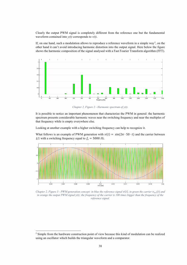
Clearly the output PWM signal is completely different from the reference one but the fundamental waveform contained into y(t) corresponds to v(t).
If, on one hand, such a modulation allows to reproduce a reference waveform in a simple way5, on the other hand it can’t avoid introducing harmonic distortion into the output signal. Here below the figure shows the harmonic composition of the signal analysed with a Fast Fourier Transform algorithm (FFT).
Chapter 2, Figure 2 - Harmonic spectrum of y(t).
It is possible to notice an important phenomenon that characterize the PWM in general: the harmonic spectrum presents considerable harmonic waves near the switching frequency and near the multiples of that frequency while is empty everywhere else.
Looking at another example with a higher switching frequency can help to recognize it.
What follows is an example of PWM generation with 𝑣(𝑡) = sin(2𝜋 ∙ 50 ∙ 𝑡) and the carrier between ±1 with a switching frequency equal to 𝑓𝑠 = 5000 Hz.
Chapter 2, Figure 3 - PWM generation concept: in blue the reference signal 𝑣(𝑡), in green the carrier 𝑣𝑡𝑟𝑖(𝑡) and in orange the output PWM signal y(t); the frequency of the carrier is 100 times bigger than the frequency of the
reference signal.
5 Simple from the hardware construction point of view because this kind of modulation can be realized using an oscillator which builds the triangular waveform and a comparator.

39
Chapter 2, Figure 4 - - Harmonic spectrum of the new y(t).
These results show that the most relevant harmonic waves are near to the switching frequency furthermore it is possible to recognize the same behaviour in terms of harmonic amplitude. This happens because the ratio 𝑚𝑎, between the peak value of the carrier and the peak value of the reference wave, is the same in the two cases and it is a value between 0 and 16.
𝑚𝑎 =𝑉𝑟𝑒
𝑉𝑡𝑟𝑖
In the next table it is shown the harmonic content of the PWM output wave with different 𝑚𝑎 and for different ratios between the switching frequency and the fundamental one, called modulation frequency ratio.
𝑚𝑓 =𝑓𝑠𝑓1
HARMONIC CARDINAL NUMBER
𝑚𝑎 = 0.2 𝑚𝑎 = 0.4 𝑚𝑎 = 0.6 𝑚𝑎 = 0.8 𝑚𝑎 = 1.0
1 (fundamental) 0.2 0.4 0.6 0.8 1.0
𝑚𝑓 𝑚𝑓 ± 2 𝑚𝑓 ±4
1.242 0.016
1.15 0.061
1.006 0.131
0.818 0.220
0.601 0.318 0.018
2𝑚𝑓 ± 1 2𝑚𝑓 ±3 2𝑚𝑓 ±5
0.190 0.326 0.024
0.370 0.071
0.314 0.139 0.013
0.181 0.212 0.033
3𝑚𝑓 3𝑚𝑓 ± 2 3𝑚𝑓 ±4 3𝑚𝑓 ±6
0.335 0.044
0.123 0.139 0.012
0.083 0.203 0.047
0.171 0.176 0.104 0.016
0.113 0.062 0.157 0.044
6 It is possible to use references with a 𝑚𝑎 higher then one but all those kinds of modulations called overmodulation do not belong to the target of this project. For this reason they will be neglected.

40
4𝑚𝑓 ± 1 4𝑚𝑓 ± 3 4𝑚𝑓 ± 5 4𝑚𝑓 ± 7
0.163 0.012
0.157 0.070
0.008 0.132 0.034
0.105 0.115 0.084 0.017
0.068 0.009 0.119 0.050
Chapter 2, Table 1 - Normalized harmonic content of y(t) for 𝑚𝑓 > 9. [8]
It is useful to underline that even if the harmonic content is the same at different switching frequency, adopting a higher 𝑓𝑠 allows to filter more easily the harmonics of the voltage wave so it would be preferable to choose a high value for that frequency if the switching losses were not directly proportional with 𝑓𝑠. There is not a general rule to choose the switching frequency and it is always the result of a trade-off between costs and objectives which can consider many different aspects: to reduce the losses, power quality, a very silent electrical system, low cost electrical system and so on.
2.1.2 - PWM management in three phases inverter to feed a three phases load It is possible to feed a three phases load with an inverter as the one showed in the electrical scheme below.
A
B
C
N
Chapter 2, Figure 5 - Electrical scheme of a 3P4L inverter with a three phases load. It shows that the N leg is not used at all in the load feeding.
The main target of this application is to create three sinusoidal waveforms starting from a continuous voltage input equal to 𝑉𝑑𝑐. It is done using one triangular carrier and three sinusoidal signals which are far from each other of an angle of 120 degrees.
𝑣𝑎∗(𝑡) = 𝑉𝑀𝐴𝑋 ∙ cos(𝜔𝑡 + 𝜃0)
𝑣𝑏∗(𝑡) = 𝑉𝑀𝐴𝑋 ∙ cos (𝜔𝑡 + 𝜃0 −
2𝜋
3)
𝑣𝑐∗(𝑡) = 𝑉𝑀𝐴𝑋 ∙ cos (𝜔𝑡 + 𝜃0 −
4𝜋
3)
What follows is an example of how the three references PWM works with a ratio 𝑚𝑎 equal to 0.8 and 𝑚𝑓 = 10 where the voltage’s values are normalized.

41
Chapter 2, Figure 6 - Carrier and modulators: 𝑣𝑎∗(𝑡) in yellow, 𝑣𝑏
∗(𝑡) in blue and 𝑣𝑐∗(𝑡) in green.
Chapter 2, Figure 7 - PWM signals: the voltage 𝑉𝑎𝑁 from phase a to negative in yellow and 𝑉𝑏𝑁 from phase b to negative in blue.
Chapter 2, Figure 8 - Line to line voltage wave form called 𝑉𝑎𝑏; it comes from 𝑉𝑎𝑏 = 𝑉𝑎𝑁 − 𝑉𝑏𝑁.

42
Chapter 2, Figure 9 - Harmonic spectrum of the line to line voltage.
It is easy to recognize that the maximum value of the modulating signal, measured between O and the phase, can be half of the DC-bus voltage; because of this reason three sinusoidal references moving from +Vdc and -Vdc allow to build a voltage wave with these limitations:
𝑝ℎ𝑎𝑠𝑒 = 𝑉𝑀𝐴𝑋 =𝑉𝑑𝑐
2, remembering that 𝑉𝑀𝐴𝑋𝑝ℎ𝑎𝑠𝑒 depends by 𝑚𝑎
𝑉𝑟𝑚𝑠_𝑝ℎ𝑎𝑠𝑒 ≤1
√2∙𝑉𝑑𝑐
2
𝑉𝑟𝑚𝑠_𝑙𝑖𝑛𝑒 ≤√3
√2∙𝑉𝑑𝑐
2
𝑙𝑖𝑛𝑒 = √3 ∙𝑉𝑑𝑐
2= 0.866 ∙ 𝑉𝑑𝑐
2.2 - Homopolar injection in sine-triangular PWM Homopolar injection is a modulation technique useful to reach the target of increasing the maximum amplitude of the line to line output voltage. It basically consists on a modification of the reference signals through a common homopolar component 𝑣ℎ.
𝑣𝑎∗(𝑡) = 𝑉𝑀𝐴𝑋 ∙ cos(𝜔𝑡 + 𝜃0) + 𝑣ℎ(𝑡)
𝑣𝑏∗(𝑡) = 𝑉𝑀𝐴𝑋 ∙ cos (𝜔𝑡 + 𝜃0 −
2𝜋
3) +𝑣ℎ(𝑡)
𝑣𝑐∗(𝑡) = 𝑉𝑀𝐴𝑋 ∙ cos (𝜔𝑡 + 𝜃0 −
4𝜋
3) +𝑣ℎ(𝑡)
The core concept is to keep the voltage references as far as it is possible from the peaks of the carrier wave introducing a rise or a decrease of the references, using the mismatch between the three modulators.
What is interesting to remember is that the added voltages do not modify the continuous content of the line to line voltage and thanks to this the value of 𝑣ℎ can be chosen without limitations.
From a visual point of view is easy to recognize how the homopolar injection should be calculated.

43
Chapter 2, Figure 10 - Carrier and simplified modulators: 𝑣𝑎∗ in yellow, 𝑣𝑏
∗ in blue and 𝑣𝑐∗ in green; 𝑚𝑎 = 0.8 .
In this case one reference signal is touching the peak of the carrier; the homopolar voltage can be chosen to maximize the distance from 𝑣𝑎
∗ to the positive peak and from 𝑣𝑐∗ to the negative one, at the same time.
Chapter 2, Figure 11 - Carrier and simplified modulators: 𝑣𝑎∗ + 𝑣ℎ in yellow, 𝑣𝑏
∗ + 𝑣ℎ in blue and 𝑣𝑐∗ + 𝑣ℎ in
green; 𝑚𝑎 = 0.8 .
Applying this basic concept to a sinusoidal reference it is possible to recognize that the homopolar injection 𝑣ℎ(𝑡) looks like a triangular wave with a frequency which is the triple of the reference command wave.
Chapter 2, Figure 12 - Modulators (𝑚𝑎 = 1) with homopolar injection; the 𝑣ℎ(𝑡) changes as shown from the red line. It is possible to notice that in this figure the references have been translated by an offset of +0.5 compared
with the previous two figures.
The following figures show which advantages, in terms of voltage amplitude, can be obtained using homopolar references just a little lower than the overmodulation limit.

44
Chapter 2, Figure 13 - Single phase reference with homopolar injection at the overmodulation limit.
Chapter 2, Figure 14 - Harmonic spectrum of the previous figure. It allows to notice that the fundamental amplitude is higher than 1 even if the reference is not working in overmodulation. More specifically the fundamental wave amplitude is the sum of the DC offset of the reference and the 50 Hz content.
Chapter 2, Figure 15 - – Line to line voltage measured between two legs of an ideal inverter in which the IGBTs have been driven with two references as the one here above but 120 degrees far from each other. Note that the
DC-bus voltage of the simulation was 300 V so the line to line voltage is taking as much power as possible.

45
Chapter 2, Figure 16 - Harmonic spectrum of previous figure; there is no harmonic content.
It therefore follows that the homopolar injection PWM technique increases the voltage range production of the traditional sine triangle PWM, which was showed in a previous paragraph, allowing to reach the following limits:
𝑙𝑖𝑛𝑒 ≤ 𝑉𝑑𝑐
𝑝ℎ𝑎𝑠𝑒 = 𝑙𝑖𝑛𝑒 ∙1
√3≤
𝑉𝑑𝑐
√3
𝑉𝑟𝑚𝑠_𝑝ℎ𝑎𝑠𝑒 ≤1
√2∙𝑉𝑑𝑐
√3
𝑉𝑟𝑚𝑠_𝑙𝑖𝑛𝑒 ≤𝑉𝑑𝑐
√2
2.3 - PWM implementation with TMS320F28335 A digital signal controller TMS320F28335 has been used to implement the PWM. This device, whose specifications are more exhaustively described in Chapter1, is going to be presented especially in all those function that play a key role in the PWM implementation. In first place the logical structure of the PWM signal, then the many synchronized events that occur during a PWM cycle, the dead band signal construction and so on.
Then, because of the strong link that exists between current and voltage control and the PWM signal, in this section it has been considerate appropriate to have a look on how the analogic to digital conversion (ADC) has been implemented as it has been done dealing with PWM.
Finally, it will follow the paragraph which deals with the peculiar choices made in the actual implementation of PWM for the 3P4L inverter and at the end some tests are shown in order to verify if the implementation results are correct.
2.3.1 - TMS320F28335 ePWM module features The logic core of the PWM modulation is the production of a triangular carrier and the comparison between this carrier and the reference waveform; the first action is managed by the time base (TB) block, the second by the counter compare (CC).
TB determines timing for the all ePWM module’s events and its built-in synchronization logic allows multiple ePWM modules to work together as a single system or to synchronize TB with other peripheral modules. It can generate the following outputs: time base counter equal to specified period (PRD) and time base counter equal to zero. Inside this block there is a register that is used to specify the operation

46
mode of TB in fact it is possible to choose between Up-Down-count mode, Up-count mode and Down-count mode.
CC block takes as input the time base counter value. This value is constantly compared with the counter compare A (CMPA) and counter compare B (CMPB) registers and an output event is generated when the time-base counter is equal to one of this two compare registers.
Here below the figure shows, throw a block diagram, how is built the PWM signal in TMS320F28335;
Chapter 2, Figure 17 - ePWM building module. [9]
The action qualifier block has a crucial role in waveform construction and PWM generation because it decides which events are converted into various action types and thus producing the required switched waveforms at the EPWMxA and EPWMxB outputs.
At this point it is possible to introduce the dead band (DB) thanks to the DB’s submodule which is here reported.
Chapter 2, Figure 18 - Configuration options for dead band submodule. [9]
Thanks to the 8 switches inside the sub-module, it is possible to create 8 different dead time configurations choosing between complementary rising and falling delay, only rising edge delay, only falling edge delay or no DB delay.

47
The following block is the PWM-chopper (PC); it allows to modulate the PWM waveform generated by the action-qualifier and dead-band submodules or it can totally be bypassed as it has been chosen for the 3P4L inverter of this project.
Finally, the trip zone (TZ) allows to manage the external fault condition forcing the PWM signals to be high, low or high impedance. The output signals of this last block are the PWM signals that come out of the microcontroller; these two are sent to the drivers’ electronic boards, through optical fibre cables, and there they are used to control the drivers.
What do control the top and bottom IGBTs of one leg of the 3P4L inverter are the signals coming from the driver which are, neglecting the dead time, the opposite of the ePWM signals built into with the microcontroller.
2.3.2 - TMS320F28335 ADC module features The analogic to digital conversions can rely on a resilient hardware which ensures a fast conversion time that runs at 12.5 MHz or 6.25 MSPS (80 ns), on a 12-bit ADC core with built-in dual sample and hold (S/H) and on 16 conversion channels divided into two groups of 8 channels which allow the channels to work simultaneously. Finally, all the output data are stored in 16 results registers that can be individually addressed.
The analogic input shall move only between 0 and 3 V so the possible digital values corresponding to their inputs are the one showed here below.
ANALOG VALUE DIGITAL VALUE 0 V 0
0 𝑉 < 𝐴𝑛𝑎𝑙𝑜𝑔 𝑣𝑎𝑙𝑢𝑒 < 3 𝑉 212
3∙ 𝐴𝑛𝑎𝑙𝑜𝑔 𝑣𝑎𝑙𝑢𝑒
3 V 4096 Chapter 2, Table 2 - ADC conversions.
The following figure shows the general scheme which rules how ADC modules work; what is important to underline is that all the process can be divided and summarized in 4 steps: taking the external pin values (sampling), waiting until the values become stable (hold), converting the analogic values to digital (conversion) and saving the digital values.
Chapter 2, Figure 19 - Block diagram of the ADC module. [10]

48
Looking at the figure it is possible to get deeper in the knowledge of the working flow of this module. More precisely, the working procedure of the ADC module, that starts with the initialization of the ADC registers, take place when a start of conversion (SOC) signal arrives. After that the value of the maximum number of conversions is loaded in the appropriate register7 and thanks to this the conversion can begin. When the current conversion is completed a digital result is written into the corresponding ADC result register. This process finishes once all the conversions required in the maximum number of conversions are ended.
2.4 - PWM signal actual programming The first step consists on initializing every module; neglecting each module’s clock enabling, the DSP configuration and the configuration of all the bit which have been used for general input output purpose (GPIO), here the text deals with the ePWM and then ADC initialization. Other register as the shadow mode register or the dead band’s one has not been used so the initialization is neglected.
The second step is the core of the program (called “main”) which manage all the modules with the purpose of making the inverter works properly; for this reason, it also contains the control loops.
The code used and here described can be found into an appendix.
2.4.1 - TMS320F28335 ePWM module initializing For this inverter it has been used a symmetric triangular carrier whose frequency, in many tests, was 5 kHz in order to prevent low level harmonic disturbances and to avoid stress working condition for the IGBTs. Considering a TB clock frequency of 150 MHz the TB clock period is approximately 6.67 ns so, for the purpose of reaching a period of 200 µs (5 kHz), there must be 3000 up-down-counts in a period. This means that the Up-Down triangular wave has to be composed by 1500 up-counts and 1500 down-counts. The following figure helps in understanding how is built the carrier.
Chapter 2, Figure 20 - Time base frequency and period. [9]
This carrier is used by the four ePWM channels but in order to control them properly is necessary to set the synchronization between channels. It has been adopted a master-slave synchronization scheme where the ePWM of channel one is the master and the other three are the slaves.
7 The register depends on the conversion mode used by the device; for example, if the device is working in uninterrupted autosequenced mode, the register is ADCASEQSR.

49
Chapter 2, Figure 21 - ePWM channels synchronization scheme; ePWM1 configurated as a master while ePWM2 is configurated as a slave. [9]
Then is necessary to inform the AQ about what to do when the CC sent to it the signal that it has reached the comparison value. Here is necessary to look at the whole duty signal transmission system; the signal comes out of the DSP, through an optical fibre, arrives to the driver and finally commands its IGBT. What’s important to know is that the optical fibre inverts the signal, so it is necessary to pre-invert it to assure that the IGBT receives the correct information. Because of this, the AQ behaviour is ruled as follow:
ACTION QUALIFIER A ACTION QUALIFIER B
Action Counter UP
Action Counter DOWN
Action Counter UP
Action Counter DOWN
𝑖𝑓 𝑐𝑎𝑟𝑟𝑖𝑒𝑟> 𝑟𝑒𝑓𝑒𝑟𝑒𝑛𝑐𝑒
1
1
0
0
𝑖𝑓 𝑐𝑎𝑟𝑟𝑖𝑒𝑟< 𝑟𝑒𝑓𝑒𝑟𝑒𝑛𝑐𝑒
0
0
1
1
Chapter 2, Table 3 - Action qualifier’s settings.
The last setting initialized with an ePWM register is the ADC start of conversion event. The principle object of the ADC channels is to measure current or voltage during the modulation, possibly once each carrier period. In such a period the current present a not constant behaviour; because of the switching from 0 to 𝑉𝑑𝑐 2⁄ or vice versa, in almost the first half of the carrier period the phase current shows a very ripple affected trend so that would lead to a gross measuring error so it has been decided to start the ADC conversion in the middle of the carrier period which means under the top peak of the triangular waveform.

50
Chapter 2, Figure 22 - Time base UP-DOWN-count waveforms, synchronization events. It has been chosen the CTR=PRD event. Notice that thanks to the rapidity of the control loop it has been possible to set one ADC
conversion each period, even if there was the possibility to delay it of some period. [9]
2.4.2 - TMS320F28335 ADC module initializing The working mode is the first thing which was chosen. The figure that follows represents the autosequenced cascade mode chosen to manage the ADC module of the 3P4L inverter studied.
Chapter 2, Figure 23 - Block diagram of autosequenced ADC in cascaded mode. [10]
Then it is necessary to state the maximum number of conversion and which channels must be converted; in our case there are 8 conversion and the channels go from the first to the fourth of A register and from the first to the fourth of the B register.

51
The last fundamental thing to state is to allow the conversion sequence (SEQ) to be started by ePWM1 SOCA trigger event.
What’s fundamental to know about the code is that all the control loop and then also the measurement are made inside an ADC interruption that starts with the SOCA trigger events.
2.5 - Tests to check PWM driving signal and generated voltage In order to check the proper working behaviour of the inverter have been made many different tests. Each of these was focused on a part of the whole pulsed voltage generation structure: the DSP signal generation, each single leg voltage generation (half bridge configuration), full bridge generation and finally the entire 3 legs voltage generation.
The final test of this section shows the homopolar injection implementation results.
After these tests it is possible to state that the 3P4L inverter can properly produce a pulsed controlled voltage through a PWM modulation.
2.5.1 - PWM driving signal test The following test shows the behaviour of the ePWM1 module, corresponding to the first leg of the 3P4L, while driven with a 70% duty cycle. The top and bottom IGBT are complementary driven and there is no dead-band set into the microcontroller because it is introduced directly by the driver and its value is about 4.3 µs. The 3P4L inverter is feeding a three phases star connected electrical machine characterized by a 10 Ω phase resistance (R) and 46 mH phase inductance (L).
Here below are reported the final results of the modulations’ implementation through an image directly taken from the oscilloscope. Test’s scheme shows the testing circuit and the position of each probe and the table describe the channels characteristics. To manage all these probes and to have a high resolution it has been used the DL750 Scope Corder oscilloscope by Yokogawa.
Chapter 2, Figure 24 - Real duties and parameters while testing the PWM driving signals

52
Ch. 1
Ch. 2
Ch. 3
Ch. 4
Ch. 5
Ch. 6
Ch. 9
Driver 1
Driver 1
DSP, top IGBTPWM generation
DSP, top IGBTPWM generation
GND
GND
GND
Chapter 2, Figure 25 - Electrical scheme of the test.
.
Some comments:
The green line corresponds to the top IGBT driving signal coming from the DSP, the violet is the signal which actually drives the top IGBT, coming from the driver board. They are one the opposite of the other; this is caused by the optical fibre that brings the signal from the DSP to the driver but also inverts it.
It is possible to detect the dead time in the centre of the figure; here is reported a horizontal zoomed view focused on the dead band which is the distance between the down step of the green line, under the light blue one and the step up of the violet one. Using the grey points of the time axis, it is easy to count that this distance is just a little less than 5 µs.
Chapter 2, Figure 26 - Dead time introduced by the driver board.
A PWM period lasts 5 time-divisions so 200 µs which correspond to a 5 kHz switching frequency.
Channel 5 shows the oscillation of the line to line voltage caused by the switching of the IGBTs.

53
In channel 6 the current’s behaviour: it increases its magnitude when the load voltage is positive while decreases when zero load voltage.
SIMULATION’S PARAMETER VALUE time 50 µs/div. Ch. 1 20 V/div.
Ch. 2 (top IGBT) 2 V/div. Ch. 3 10 V/div.
Ch. 4 (bottom IGBT) 2 V/div. Ch. 5 10 V/div. Ch. 6 200 mV/div. Ch. 9 10 V/div.
Chapter 2, Table 4 - Simulation’s parameters settings.
2.5.2 - PWM generated line to line voltage test; full bridge configuration. The objective of the following test was to check the voltage generated by the inverter in full bridge configuration. It consists in feeding an RL load with a full bridge inverter configuration where one leg follows a sinusoidal reference for the duty construction while in the other the duty is fixed and equal to half of the switching period. The 3P4L’s DC-bus is fed with 85 V and the R and L, which characterize the load, are the same of the previous test.
Here below are reported the final results collected with the oscilloscope and then redrawn in MATLAB. Test’s scheme shows the testing circuit and the position of each probe.
I V
Chapter 2, Figure 27 - Electrical scheme of the test. The green circle represents the current probe position while the blue circle the position of the voltage one.
Chapter 2, Figure 28 - In blue the line to line voltage measured by the voltage probe. In red an approximation of the fundamental waveform get filtering the blue signal with a 1.5 kHz filter.

54
What’s interesting to notice is the behaviour of the pulsed voltage signal that correspond to the theoretical one.
Chapter 2, Figure 29 - In green the phase current measured by the current probe. In blue an approximation of the fundamental waveform get filtering the green signal with a 1.5 kHz filter.
Through this test it has been checked that the line to line voltage produced by the inverter is exactly the one wanted. In the current, which has the wanted wave from, it is possible to appreciate the noise produced by the IGBTs’ commutations.
Those two wave forms are obviously too “rough” to be properly controlled due to create a grid; in order to clean this wave and the voltage wave it will be necessary to put a filter between the inverter and its loads.
2.5.3 - PWM generated three phases voltage test The objective of the following test was to check the voltage generated by the inverter while feeding a three phases load such as an induction motor. Each leg is generating a sinusoidal wave and the waves, that has the same amplitude, are spaced 120 degrees from each other. The 3P4L’s DC-bus is fed with 600 V and the R and L, which characterize the load, are the same of the previous test. The switching frequency is equal to 10 kHz.
Here below are reported the final results collected with the oscilloscope and then redrawn in MATLAB. Test’s scheme shows the testing circuit and the position of each probe.
A
B
C
I
V
Chapter 2, Figure 30 - Electrical scheme of the three phases test. The green circle represents the current probe position while the blue circle the position of the voltage one.

55
Chapter 2, Figure 31 - In blue the line to line voltage measured by the voltage probe. In red an approximation of the fundamental waveform get filtering the blue signal with a 1.5 kHz filter.
What is possible to notice, looking at the line to line voltage, is that exist some moments in which the modulation doesn’t respect the theoretical behaviour. These moments are very small so that the fundamental wave is not significantly affected by their existence. In the following picture it is possible to appreciate how short they are: less than 2µs.
Chapter 2, Figure 32 - On the left: a moment of the theorical behaviour of a line to line voltage for a three phases load fed with a three phases voltage system. On the right a zoom of the x axis of the previous figure.
From this comparison it is easy to detect a problem in the IGBTs synchronization looking at the biggest difference between a period of the right wave and a period of the left one. The not perfect synchronization generates those peaks that reach -200 V.
Chapter 2, Figure 33 - In green the phase current measured by the current probe. In blue an approximation of the fundamental waveform get filtering the green signal with a 1.5 kHz filter.
The behaviour of the current is not exactly sinusoidal but the deviation is very small.
Thanks to this test it has been corrected the not perfect synchronization between the IGBTs.

56

57
Chapter 3: Current Control (CC)
This chapter deals with the design, implementation and test of a current control. Especially, this is not the final version of CC that the inverter uses to form the grid but a very similar one; the global schemes of these two are equals but they are different in the PI controller tuning.
With the purpose of giving a clear view of the final structure of this control the chapter will be divided in two main section; the first about the current control implementation in MATLAB (for simulated tests) and in the DSP (for experimental tests), the second about the experimental results and control improvements.
To have a clear division between the schemes that represents existing things and those which represents logical control schemes, all the control schemes will be shown using the Simulink model representations.
3.1 – CC implementation Here is introduced the scheme which has been used for all the current control loops. Then it will be described in all its components and parameters.
Chapter 3, Figure 1 - Current control loop. This control allows to regulate the current which flows out of the inverter.
For a higher precision of the real cabinet representation, many simulations have been made twice: once in continuous time domain and then in discretized time domain. Due to this fact, some pages will be dedicated to describe how these two analysis are structured.
The only difference in the discrete time analysis is related to the control of the inverter. This mean that the Simulink’s system doesn’t change8 but the regulators and some general settings.
8 This happens because of the use of the Simulink’s tool called powergui that allows to divide the system in two parts: the transfer functions part and the electric part. So that the modifies for a discrete time analysis must be done only in the transfer functions part.

58
3.1.1 – Scheme for continuous time analysis What follows is the CC loop scheme including the blocks which generate the angle of the current, three blocks in the top left, and the powergui block, in the top right of the figure.
Chapter 3, Figure 2 - Current control loop for continuous time analysis.
Looking at the d-axis CC loop is possible to recognize the following blocks: the step, the sum, the regulator, the reference conversion block, the inverter, some current sensor, the load and, in the feedback, one more reference conversion block; let’s analyse the more relevant ones.
With the purpose of controlling currents whose reference are step signals, it has been chosen a first order regulator which grants a null error in steady state conditions: a proportional integral one which belongs to the PID control family and can be generally described as follow:
𝑢(𝑡) = 𝑘𝑃 ∙ 𝑒(𝑡) + 𝑘𝐼 ∙ ∫ 𝑒(𝑡)𝑑𝑡𝑡
𝑡0
+ 𝑘𝐷 ∙𝑑𝑒(𝑡)
𝑑𝑡, 𝑤ℎ𝑒𝑟𝑒 𝑘𝐷 = 0.
It has been implicitly considered that 𝑢(𝑡) is the output of the PI block (the letter u reminds that the output signal of the CC loop is a voltage value) and 𝑒(𝑡) is the input.
To tune the PI controller on the plant G(s) it has been used the zero-pole cancellation strategy that is here synthetically showed.
𝐺(𝑠) =1
𝑅 + 𝑠 ∙ 𝐿
𝑃𝐼(𝑠) ∙ 𝐺(𝑠) = (𝑘𝑃 +𝑘𝐼
𝑠) ∙ (
1
𝑅 + 𝑠 ∙ 𝐿)
In which it is possible to remove the pole of the plant taking the gains as follow:
𝑘𝑃_𝑖 = 𝑠 ∙ 𝐿 = 2𝜋 ∙ 𝑏𝑤 ∙ 𝐿
𝑘𝐼_𝑖 = 𝑠 ∙ 𝑅 =𝑅
𝐿∙ 𝑘𝑃_𝑖
The signals that exit from the PI blocks are then converted from dq coordinates to abc; this transformation and the reverse one has been implemented in the following ways:

59
𝑇𝑑𝑞→𝑎𝑏𝑐 = [
cos 𝜃𝑑𝑞 −sin 𝜃𝑑𝑞 1
cos(𝜃𝑑𝑞 − 2𝜋 3⁄ ) −sin(𝜃𝑑𝑞 − 2𝜋 3⁄ ) 1
cos(𝜃𝑑𝑞 − 4𝜋 3⁄ ) −sin(𝜃𝑑𝑞 − 4𝜋 3⁄ ) 1
]
𝑇𝑎𝑏𝑐→𝑑𝑞 =2
3∙ [
cos 𝜃𝑑𝑞 cos(𝜃𝑑𝑞 − 2𝜋 3⁄ ) cos(𝜃𝑑𝑞 − 4𝜋 3⁄ )
− sin 𝜃𝑑𝑞 −sin(𝜃𝑑𝑞 − 2𝜋 3⁄ ) −sin(𝜃𝑑𝑞 − 4𝜋 3⁄ ) 1
1 2⁄ 1 2⁄ 1 2⁄
]
The next relevant block is the one used to simulate the inverter; it is shown in the following figure.
Chapter 3, Figure 3 - Three-phase inverter for Simulink analysis.
Its DC-bus is an infinite power one created with two voltage sources each one characterized by a half of the total DC-bus voltage, the six IGBTs has an ideal behaviour and they are commanded by the duty signals.
Finally, the load block:
Chapter 3, Figure 4 - Three-phase star connected RL load used in the simulations and in the tests.

60
3.1.2 – Scheme for discretized time analysis It is necessary to implement a discretized control inside the DSP and this is why it was implemented a discretized control in Simulink in order to check how does such a control actually behaves. The minimum time step unit of the discretization which correspond to the sampling time of the simulation has been called 𝑇𝑠 and it is equal to the period of the triangular waveform generated into the DSP.
What follows is the discretization of the PI controller using Tustin’s method.
𝑘𝑃 ∙ 𝑠 + 𝑘𝐼
𝑠 , 𝑤𝑖𝑡ℎ 𝑠 =
2
𝑇𝑠
∙𝑧 − 1
𝑧 + 1
𝑘𝑃 +𝑘𝐼
𝑠= 𝑘𝑃 + 𝑘𝐼 ∙ (
𝑇𝑠
2∙𝑧 + 1
𝑧 − 1) = 𝑘𝑃 +
𝑘𝐼 ∙ 𝑇𝑠
2 ∙ (𝑧 − 1)∙ (𝑧 + 1) =
2𝑘𝑃 ∙ (𝑧 − 1) + 𝑘𝐼 ∙ 𝑇𝑠 ∙ (𝑧 + 1)
2 ∙ (𝑧 − 1)=
=2𝑘𝑃 ∙ 𝑧 − 𝑘𝑃 + 𝑘𝐼 ∙ 𝑇𝑠 ∙ 𝑧 + 𝑘𝐼 ∙ 𝑇𝑠
2 ∙ (𝑧 − 1)=
𝑧 ∙ (2𝑘𝑃 + 𝑘𝐼 ∙ 𝑇𝑠) − 2𝑘𝑃 + 𝑘𝐼 ∙ 𝑇𝑠
2 ∙ (𝑧 − 1)=
=𝑧 ∙ (𝑘𝑃 +
𝑘𝐼 ∙ 𝑇𝑠
2) − 𝑘𝑃 +
𝑘𝐼 ∙ 𝑇𝑠
2(𝑧 − 1)
What follows is the re-built formula of the PI controller used inside the microprocessor considering the following block scheme:
Chapter 3, Figure 5 - PI control block.
𝑈(𝑧)
𝐸(𝑧)=
𝑧 ∙ (𝑘𝑃 +𝑘𝐼 ∙ 𝑇𝑠
2) − 𝑘𝑃 +
𝑘𝐼 ∙ 𝑇𝑠
2(𝑧 − 1)
=𝑧−1 ∙ [(𝑘𝑃 +
𝑘𝐼 ∙ 𝑇𝑠
2) ∙ 𝑧 − 𝑘𝑃 +
𝑘𝐼 ∙ 𝑇𝑠
2]
1 − 𝑧−1=
=𝑘𝑃 +
𝑘𝐼 ∙ 𝑇𝑠
2− 𝑧−1 ∙ 𝑘𝑃 + 𝑧−1 ∙
𝑘𝐼 ∙ 𝑇𝑠
21 − 𝑧−1
=𝑘𝑃 +
𝑘𝐼 ∙ 𝑇𝑠
2− 𝑧−1(𝑘𝑃 −
𝑘𝐼 ∙ 𝑇𝑠
2)
1 − 𝑧−1
Let’s call:
𝑀1𝑖 = 𝑘𝑃 +𝑘𝐼 ∙ 𝑇𝑠
2 𝑎𝑛𝑑 𝑀2𝑖 = 𝑘𝑃 −
𝑘𝐼 ∙ 𝑇𝑠
2
So that:
𝑈(𝑧)
𝐸(𝑧)=
𝑀1𝑖 − 𝑧−1𝑀2𝑖
1 − 𝑧−1
Then:
𝑈(𝑧) ∙ (1 − 𝑧−1) = 𝐸(𝑧) ∙ (𝑀1𝑖 − 𝑧−1𝑀2𝑖)
For the purpose of distinguish the events that are linked with different moments, a new notation is now introduced where k reveals the present instant and k-1 indicates the previous one.
𝑈𝑘 − 𝑈𝑘−1 = 𝑀1𝑖 ∙ 𝐸𝑘 − 𝑀2𝑖 ∙ 𝐸𝑘−1
𝑈𝑘 = 𝑈𝑘−1 + 𝑀1𝑖 ∙ 𝐸𝑘 − 𝑀2𝑖 ∙ 𝐸𝑘−1

61
Such a discretization is set into the Simulink simulation through this MATLAB-function block whose function is reported below.
Chapter 3, Figure 6 - The d-axis PI controller blocks used in the Simulink analysis; it is called PIi_d.
function ud_ref = PIi_d(err_id_k1,M1i,M2i,Vlim)
persistent u_k0 %local variable persistent u_k1 %local variable persistent err_id_k0 %local variable
if(isempty(u_k0)) u_k0=0; end if(isempty(err_id_k0)) err_id_k0=0; end
u_k1=u_k0+M1i*err_id_k1-M2i*err_id_k0;
if abs(u_k1)>abs(Vlim) %saturation u_k1=Vlim*sign(u_k1); end
u_k0=u_k1; err_id_k0=err_id_k1; ud_ref=u_k1;
Chapter 3, Figure 7 - PIi_d block function.

62
3.2 – CC simulations, tests and improvements At this point of the work may simulations and tests were executed to discover any kind of problem in the cabinet also because the assembling of the whole cabinet has been realized just before beginning these CC tests. In the following paragraphs will be shown only the main ones.
The goal of the following tests was to verify the right working operations of the current control loop.
Many kind of problems can occur while testing a prototype and they can be related to the hardware or to the software or to the supplies or to several other things. Here it is only remembered a problem related to the control: the saturation of the control signal which causes an excess overshooting in PI controllers called windup.
In order to solve any windup problem due to the saturation of the control signal, it is used a realizable references anti windup strategy. [11]
3.2.1 - Realizable references anti-windup technique: implementation Windup is a phenomenon directly linked to the PI controllers; it can arise when the controller current demand exceeds the maximum current available in the real system. Such a real current can have a maximum because of the power limit of the supply source or because of some thermal limit. This threshold has to be introduced into the control scheme.
When the control signal saturates (: reaches the threshold), it won’t rise more but the integral component, calculated by the PI control, will. If the controlled system is stable, then the error will decrease until zero and after this the integral component starts to decrease. During the time of the falling to zero of the PI’s integral component signal, there will be an overshoot of the current. The second effect of such a behaviour is a larger settling time.
In order to easily acknowledge the core idea on which this anti-windup strategy is based, let’s focus on the following control scheme.
Chapter 3, Figure 8 - Global structure of the implemented real reference strategy adopted.
The figure represents the PI control structure where u is the input of the controller and y the output. The block called discretized_PI represent contains the function PIi_d showed in the previous figure but now the variables u_k0 does not depends on the variable u_k1 but on y. Thanks to this recalculated instruction the integral component of the control signal doesn’t exceed its rising.
The final PI implementation, including the realizable reference anti-windup strategy, is made as follow:

63
3.2.2 – Continuous reference CC: null theta The simplest control is the feedback control with continuous references so the first test deal with it. Null theta means that the rotation angle of the d-axis is null so that the d and q axis signals are related to the a,b,c signal through this equations:
𝑇𝑑𝑞0→𝑎𝑏𝑐 = [
1 0 1
−1 2⁄ √3 2⁄ 1
−1 2⁄ −√3 2⁄ 1
]
By the way the null theta condition can be implemented into the control strategy assuming a null frequency f.
The test consists in controlling the current powering a RL three phase load using the control scheme described above here with the following parameters while the d-axis current changes from 0 A to 1 A and the q-axis current signal doesn’t move from 0 A.
PARAMETER VALUE Bandwidth (bw) 300 Hz
R 10 Ω L 42 mH
𝑘𝑃_𝑖 79.1681 𝑘𝐼_𝑖 1.8850e+04 𝑇𝑠 0.2e-03
𝑉𝐷𝐶𝑏𝑢𝑠 300 V 𝑉𝑠𝑎𝑡𝑢𝑟𝑎𝑡𝑖𝑜𝑛 20 V
Chapter 3, Table 1 - Main parameters of the CC simulations and tests.
It is possible to appreciate that in steady state conditions the current reaches the reference signal of 1 A and it demonstrate that the CC behaves properly after the transient.
function ud_ref = PIi_d(err_id_k1,M1i,M2i,Vlim)
persistent u_k0 %local variable persistent u_k1 %local variable persistent err_id_k0 %local variable
if(isempty(u_k0)) u_k0=0; end if(isempty(err_id_k0)) err_id_k0=0; end
u_k1=u_k0+M1i*err_id_k1-M2i*err_id_k0;
if abs(u_k1)>abs(Vlim) %saturation u_k1=Vlim*sign(u_k1); err_id_k1=(u_k1-u_k0+err_id_k0*M2i)/M1i; %Real references correction end
u_k0=u_k1; err_id_k0=err_id_k1; ud_ref=u_k1;
Chapter 3, Figure 9 - Final PI implementation.

64
The following image shows how the d-axis current (red line) follows a d-axis current reference signal step from 0 to 1 A.
Chapter 3, Figure 10 - Static reference test: response to a step from 0 to 1A; behaviour of the phase a current.
SIMULATION’S PARAMETER VALUE time 1 ms/div. Ch. 5 0.5 A/div.
Chapter 3, Table 2 - Oscilloscope’s parameters settings.
The rise of the current until the 95% of the step value lasts approximately 1.6ms.
The regulator is as fast as wanted because imposing a bw of 300 Hz corresponds to ask to the signal to reach the 95% of the reference in:
𝑡95% =3
2𝜋 ∙ 𝑏𝑤= 1.6 𝑚𝑠
What follows are the results obtained simulating the current control loop with MATLAB and Simulink.
Chapter 3, Figure 11 - Static reference simulation: response to a step from 0 to 1A; in green the d-axis control voltage signal, in yellow the reference signal step, in red the d-axis current signal and in light blue the error
between the reference and the actual current.

65
In the upper figure it is easy to recognize the saturation of the d axis voltage control signal which lasts a few more than 1.2 ms while in the lower one is shown the rise of the current that lasts 1.6 ms which behaves very similarly to the measured current shown.
Chapter 3, Figure 12 - Static reference simulation: response to a step from 0 to 1A; a zoom of the previous figure.
3.2.3 – Rotating reference CC with realizable references The final goal of this test is to check the waveform of the current produced by the inverter when the reference is a sinusoidal wave moving at 50 Hz. Because of this it has been set a rotating theta whose angular speed is:
𝜔 = 2𝜋 ∙ 50
The test’s settings and the reference signal are the same used in the previous test.
When the d-axis current reference signals changes from 0 A to 1 A and the q-axis current signal doesn’t move from 0 A, the final behaviour of the current is the red line of the following figure.
Chapter 3, Figure 13 - Rotating reference test; Steady state condition.

66
SIMULATION’S PARAMETER VALUE time 5 ms/div. Ch. 1 100 V/div. Ch. 2 50 V/div. Ch. 3 100 V/div. Ch. 5 100 V/div.
Chapter 3, Table 3 - Oscilloscope’s parameters settings.
The captured waveform has not been filtered at all during the measurement so that it is possible too notice some pulses that exits from their correct range; neglecting these is easy to recognize that:
the amplitude of the current flowing in phase a of the load is exactly 1 A as asked by the reference signal.
the frequency of the current wave is exactly 50 Hz.
Chapter 3, Figure 14 - Rotating reference simulation; Steady state condition.
In the simulation is shown the ideal behaviour the inverter when controlled with the same current control adopted in the test. A synthetic legend of the waveforms is reported here below.
WAVEFORM (colour) AND AXIS SCALE Time 1:1
DC-bus voltage (yellow) 1:100 Phase voltage (green) 1:50
Phase a current 1:1
Chapter 3, Table 4 - Waveform and axis scales associated to the rotating reference simulation’s figure.

67
Chapter 4: Voltage Control (VC)
Voltage control is the last step of this thesis work.
The objectives of this chapter are to describe the structure of the voltage control loop adopted and to show how the inverter replies to a load disturbance while grid forming.
Here, the text deals with the cascade control of the voltage loop and its many improvements (from the feed forward to the pre-filters), with the basic grid filter design, with the inverter’s tests and some cabinet’s hardware modifies.
4.1 – VC implementation A chronological description of the whole process followed to implement the VC would be unnecessarily complex and boring so that these pages will only describe the most relevant steps introducing some theoretical key concept. The first of these is the cascade control structure concept.
4.1.1 – Cascade control It is a kind of many levels control system with an inner loop, which is times faster than the outer one, that allows to manage the control of many signals. Here the figure of a general cascade control with two levels.
Chapter 4, Figure 1 - Blocks representation of a general cascade control.
In the application we are studying the inner loops is dedicated to the control of the current which comes out of the inverter and flows into the L component of the grid filter while the outer loop controls the voltage of the terminals of the cabinet where loads can be connected which is the same voltage that refers to the capacitors of the grid filter. The figure shows this cascade control.

68
Chapter 4, Figure 2 - Cascade control concept.
The image is full of names and blocks that is useful define clearly because they will often appear in this chapter. Td is the conversion block which converts signals from dq to abc coordinate (in the previous chapter it was called: from dq to abc). Ta is the block which gives the opposite transformation and, in chapter 3 it was called: from abc to dq. The inverter’s block is exactly the same that was shown in Chapter 2, while the other blocks will be described after.
It is now necessary to introduce the grid filter characteristics.
4.1.2 – Grid filter basic design Such an inverter, which produces a voltage signal through a PWM method, needs a grid filter in order to clean its voltage waveform and connect to or form a grid.
There are mainly 3 typology of grid filters: L filters, LC filters and LCL filters. Even if LCL filters are preferred over the other for grid-connected voltage-source inverters because of their higher harmonics attenuation and smaller dimensions and weight [12], considering the complexity of such a filter design and the luck of time, it has been chosen to design a LC grid filter.
The guide lines followed in designing the filter have been obtained from [13] but from the very beginning two main criteria emerged: to use the L components already present in the laboratory’s storage and avoid filtering the 5th and the 7th harmonics because they are the main harmonics which a connected diodes rectifier would absorb.
The coils characteristics were: maximum current of 15 A and inductance at 50 Hz of 1.464 mH. Considering that the range for the cut off frequency of the low pass filter is not lower than 400 Hz, to be sure of avoiding the 7th harmonic, nor higher than 500 Hz, to reduce as much as possible the harmonic content. The initial choice was to buy a star connected capacitors of 27 µF each but the provider couldn’t supply such a device in short time so that the designed filter and control were changed, and a delta connected three-phase capacitor of 83.7 µF was bought.
The final cut off frequency is:
𝑓𝑐𝑢𝑡_𝑜𝑓𝑓 =1
2𝜋 ∙ √𝐶𝑓𝑖𝑙𝑡𝑒𝑟 ∙ 𝐿𝑓𝑖𝑙𝑡𝑒𝑟
=1
2𝜋 ∙ √83.7 ∙ 10−6 ∙ 1.464 ∙ 10−3≅ 455 𝐻𝑧
In the following figures it is possible to recognize how the filter coils and capacitors are actually connected.

69
Chapter 4, Figure 3 - Actual grid filter’s connection.
Chapter 4, Figure 4 - The coils in yellow and the delta connected capacitors into the silver cylindrical-shape container with the black terminals slot at the top.
Because of this configuration the feedback of the voltage loop takes the line to line voltages and this means that some modifies must be adopted into the transformation block Ta_v.
The redesigned transformation matrix from ab,bc,ca to dq becomes:
𝑇𝑎𝑏,𝑏𝑐,𝑐𝑎→𝑑𝑞 =1
3∙
[ cos 𝜃𝑑𝑞 −
1
√3sin 𝜃𝑑𝑞
2
3sin 𝜃𝑑𝑞 − (cos 𝜃𝑑𝑞 +
1
√3sin 𝜃𝑑𝑞)
− (sin 𝜃𝑑𝑞 +1
√3cos 𝜃𝑑𝑞)
2
3cos 𝜃𝑑𝑞 sin 𝜃𝑑𝑞 −
1
√3cos 𝜃𝑑𝑞
1 1 1 ]

70
4.1.3 – Feed forward In order to improve the behaviour of the inner control loop it is introduced a feed forward control. This type of control has a very interesting characteristic: the feed forward acts in the same moment when the disturbance takes place while a conventional feedback control needs to wait until the effects of the perturbation have been experienced. If it is possible to build a perfect model of the system, the feed forward could delate completely the effect of the disturbance.
Chapter 4, Figure 5 - Feed forward general scheme.
This method presents also some drawbacks like the fact that a not perfect system’s model leads to a permanent offset in the control. What’s important to consider is that the effectiveness of this control is directly linked to the possibility of properly modelize the system.
The system that this text is analysing allows a very simple and successful feedforward control. The key concept is to consider the phases voltages as disturbances that acts just after the CC loop. But such a feedforward doesn’t need any system model; this disturbance can be added to the inverter reference signal coming out from the current’s PI regulator with the purpose of deleting the disturbance itself. This allows to the CC regulator to manage softly but quickly the control loop.
The next image helps in recognizing how Figure 2 of Chapter 3 should be modified to consider the delta connection of the grid filter capacitors and the feedforward control.
Chapter 4, Figure 6 – Feed forward implementation.
There are three points where to measure the grid voltage with the delta connection of the capacitors and the measured voltages are Vab, Vbc and Vca and the transformation matrix Ta_v is 𝑇𝑎𝑏,𝑏𝑐,𝑐𝑎→𝑑𝑞. The two current references id_ref and iq_ref are the output signals of the PI voltage regulators and the vd and vq signals are their feedbacks.

71
4.1.4 – Pre-filter (PF) The adopted prefilters, one for each axis, allows to smooth the voltage PI overshoot and to slow down the VC loop. It basically consists in a low pass-filter like this:
𝑃𝐹(𝑠) =𝑝
𝑠 + 𝑝 , 𝑤𝑖𝑡ℎ 𝑝 =
𝑘𝐼_𝑣
𝑘𝑃_𝑣
Where p is the pole and they are inserted as follow in the control scheme:
Chapter 4, Figure 7 – Pre-filter implementation’s structure.
4.1.5 – Pre-filter discretization It is necessary to implement a discretized control inside the DSP and this is why it was implemented a discretized control in Simulink in order to check how does such a control actually behaves. The minimum time step unit of the discretization which correspond to the sampling time of the simulation has been called 𝑇𝑠 and it is equal to the period of the triangular waveform generated into the DSP.
What follows is the discretization of the PF using Tustin’s method.
𝑃𝐹(𝑠) =𝑝
𝑠 + 𝑝 , 𝑤𝑖𝑡ℎ 𝑠 =
2
𝑇𝑠
∙𝑧 − 1
𝑧 + 1
𝑝
𝑠 + 𝑝=
𝑝 ∙ 𝑇𝑠
2 + 𝑝 ∙ 𝑇𝑠∙ (𝑧 + 1)
𝑧 +𝑝 ∙ 𝑇𝑠 − 2𝑝 ∙ 𝑇𝑠 + 2
, 𝑤𝑖𝑡ℎ 𝑝 =𝑘𝐼_𝑣𝑜𝑙𝑡𝑎𝑔𝑒𝑙𝑜𝑜𝑝
𝑘𝑃_𝑣𝑜𝑙𝑡𝑎𝑔𝑒𝑙𝑜𝑜𝑝
Let’s assume that 𝐺 = 𝑝 ∙ 𝑇𝑠 ,
𝑝
𝑠 + 𝑝=
𝐺2 + 𝐺
∙ (𝑧 + 1)
𝑧 +𝐺 − 2𝐺 + 2
=
𝑧−1 ∙ (𝐺
2 + 𝐺∙ (𝑧 + 1))
1 +𝐺 − 2𝐺 + 2
∙ 𝑧−1
What follows is the re-built formula of the PI controller used inside the microprocessor considering U as the input signal of the PF and Y as its output signal.

72
Chapter 4, Figure 8 - Prefilter block.
𝑌(𝑧)
𝑈(𝑧)=
𝑧−1 ∙ (𝐺
2 + 𝐺∙ (𝑧 + 1))
1 +𝐺 − 2𝐺 + 2
∙ 𝑧−1
So that:
𝑌𝑘 ∙ (1 +𝐺 − 2
𝐺 + 2∙ 𝑧−1) = 𝑈𝑘 ∙ (
𝐺
2 + 𝐺∙ 𝑧−1 +
𝐺
2 + 𝐺)
𝑌𝑘 + 𝑌𝑘−1 ∙𝐺 − 2
𝐺 + 2= 𝑈𝑘−1 ∙
𝐺
2 + 𝐺+ 𝑈𝑘 ∙
𝐺
2 + 𝐺
𝑌𝑘 = 𝑈𝑘−1 ∙𝐺
2 + 𝐺+ 𝑈𝑘 ∙
𝐺
2 + 𝐺− 𝑌𝑘−1 ∙
𝐺 − 2
𝐺 + 2
4.1.6 – Final VC and CC cascade control structure What follows is the final structure of the control scheme adopted to simulate the whole “inverter and micro-grid” system in Simulink.
Chapter 4, Figure 9 - Final grid forming control configuration.
In the top left it is possible to see the discretized angle generator function called timeDiscr, below the control scheme composed by all the elements described in this chapter and in the previous one.

73
4.2 – VC simulations and tests At this point a synthetic description of the testing area is given with the purpose of helping the reader in being more comfortable when the tests’ settings and results will be shown in the following sections.
The tests consisted in measuring the voltage waveform behaviour of the formed grid while a load connects to it or disconnects from it. Then the oscilloscope and many isolated probes were needed. On the other hand the DC power source to feed the bus and the pc to run the program into the microprocessor had to be as near as possible to the cabinet in order to avoid long cables; they had been set at the right of the cabinet one upon the other. Neglecting the cabinet, the last fundamental component was the load connection circuit that was located at the feet of the cabinet’s sustaining structure.
This figure shows the whole testing area.
Chapter 4, Figure 10 - Testing area.
4.2.1 – Tests settings introduction Dealing with the tests it is necessary to describe the main equipment used. Let consider the global grid forming system as composed by four elements: the DC power source, the 3P4L inverter, a load and the connecting switch between the load and the inverter.

74
230 VAC source
DC power source
DC bus
3P4L Micro-grid
Switch
AC micro-gridbus
Chapter 4, Figure 11 – Global circuit structure of the tested system.
The DC power source is a laboratory power supply called EA-PS 8000 2U 640W - 3000W made by Electro-Automatic gmbH. It can be managed through an analogue interface that allows to move from 0 to 720 V and from 0 to 15 A. The main characteristics of such a power supply are listed in the following table.
TECHNICAL DATA EA-PS 8000 2U 640W - 3000W Input voltage 90 …264V
Frequency 45 …65 Hz Power factor correction >0.99
Output voltage 0 …720 V Output current 0 …15 A Output power 0 …3000 W
Chapter 4, Table 1 - DC power supply technical data. [14]
The load is a three phases resistance of 133 Ω in each phase and it is shown in the figure.
Chapter 4, Figure 12 - Test’s load.
The connection between load and inverter was managed by a manual switch at the beginning but because of the not perfect synchronization between the 3 switches the device was substituted with an automatic one.

75
Chapter 4, Figure 13 - The manual switch in the left, the automatic switch and its red command button in the right.
The next figure shows what is the problem of the not perfectly synchronized manual switch.
Chapter 4, Figure 14 - The current (red line) starts to rise when the switch is closing but it closes the three phases in 2 different time: first it closes 2 phases, the current flows through a total impedance of 𝑍𝑝ℎ ∙ 4 2⁄ and
then, when it closes the last one, the current flows through a total impedence of 𝑍𝑝ℎ ∙ 3 2⁄ , where 𝑍𝑝ℎ is the impedance of each phase.

76
There will be shown the results obtained imposing a voltage d-axis reference of 230 V which is a limit because the coil started to make a very bad noise and to warm up9 dangerously because, as said above, it is not a coil for high frequency applications but a device coming from the storage of the lab.
The results will also be divided between:
NO LOAD GRID VOLTAGE DISTURBANCE WHEN THE LOAD CONNECTS DISTURBANCE WHEN THE LOAD DISCONNECTS
4.2.2 – Continuous reference VC: null theta As done testing the CC loop, the results will be shown starting from the null theta condition.
The test consists in controlling the voltage powering a R three phase load using the control scheme described here above with the following parameters while the d-axis voltage changes from 0 V to 230 V and the q-axis voltage signal doesn’t move from 0 V.
TEST SETTING PARAMETER VALUE Bandwidth (current loop) 300 Hz Bandwidth (voltage loop) 15 Hz
R 133 Ω 𝑘𝑃_𝑖 (current loop) 79.1681 𝑘𝐼_𝑖 (current loop) 1.8850e+04 𝑘𝑃_𝑣 (voltage loop) 0.4 𝑘𝐼_𝑣 (voltage loop) 40
𝑇𝑠 0.2e-03 𝑉𝐷𝐶𝑏𝑢𝑠 600 V
𝑉𝑠𝑎𝑡𝑢𝑟𝑎𝑡𝑖𝑜𝑛 (current loop) 300 V 𝑉𝑠𝑎𝑡𝑢𝑟𝑎𝑡𝑖𝑜𝑛 (voltage loop) 10 A
Chapter 4, Table 2 - Main parameters of the CC simulations and tests.
It is possible to appreciate that in steady state conditions the Vab voltage reaches almost perfectly, the reference signal of
𝑉𝑎𝑏 = 𝑉𝑑 ∙3
2= 230 ∙ 1.5 = 345 𝑉
and it demonstrate that the VC behaves properly after the transient.
9 This happens because, at high frequency (our pulsating voltage frequency is 5 kHz), a sinusoidal current tries to flow as near the cable’s surface as it can. The “skin” of the conductor, that is used to make the coils, can be calculated as follow: 𝛿 = √2𝜌 𝜔𝜇⁄ , where ρ is the conductor’s resistivity, 𝜔 = 2𝜋 ∙ 𝑓 , and µ is the magnetic permeability of the conductor which in this case can be considered equal to 𝜇0. Than the current density J, at the depth d from the cable surface, is equal to: 𝐽 = 𝐽0 ∙
𝑒−𝑑 𝛿⁄ , where 𝐽0 is the current density measured on the cable surface. This generates intense Joule losses. The described phenomenon is called skin effect.

77
The following image shows how the voltage Vab (orange line) follows a d-axis voltage reference signal step from 0 to 230 V.
Chapter 4, Figure 15 - NO LOAD GRID VOLTAGE test: response to a step from 0 to 230 V; in orange the behaviour of the line to line Vab voltage, in yellow the DC-bus voltage and in red the phase a current.
OSCILLOSCOPE’S PARAMETERS VALUE time 10 ms/div. Ch. 1 200 V/div. Ch. 5 0.5 A/div. Ch. 6 100 V/div.
Chapter 4, Table 3 - Oscilloscope’s parameters settings.
The rise of the voltage until the 95% of the step value lasts approximately 32ms.
The regulator is as fast as wanted because imposing a bw of 15 Hz corresponds to ask to the signal to reach the 95% of the reference in:
𝑡95% =3
2𝜋 ∙ 𝑏𝑤≅ 32 𝑚𝑠
Let’s have a look of the both test and simulation voltages behaviour together:

78
Chapter 4, Figure 16 - Test and simulation comparison; in blue the Vab coming from simulation, in orange the measured Vab voltage. The difference between the two at steady state condition is less than 10 V.
The two signals show the same behaviour but a small (less than 3%) error at steady state condition, probably due to an imperfection during the tuning of the voltage sensors.
Now let’s check the disturbance response of the VC looking at the following figures taken during the experimental tests, which have the same axis values shown in the previous table.
Chapter 4, Figure 17 - DISTURBANCE WHEN THE LOAD CONNECTS test: response to the load connection; in orange the behaviour of the line to line Vab voltage, in yellow the DC-bus voltage and in red the phase a current.

79
Chapter 4, Figure 18 - Test and simulation comparison; in blue the Vab coming from simulation, in orange the measured Vab voltage. The difference between the two at steady state condition is less than 10 V.
The behaviour of the two signals differs a little: focusing on what happens after the load connection it is possible to notice that the signal of the real test presents a longer oscillation.
Chapter 4, Figure 19 - DISTURBANCE WHEN THE LOAD DISCONNECTS test: response to the load disconnection; in orange the behaviour of the line to line Vab voltage, in yellow the DC-bus voltage and in red
the phase a current.
Thanks to the following graph it is possible to appreciate that in this case simulation and experimental test behave almost identically, in particular the longer oscillation in the real load disconnection response doesn’t appear.

80
Chapter 4, Figure 20 - Test and simulation comparison; in blue the Vab coming from simulation, in orange the measured Vab voltage. The difference between the two at steady state condition is less than 10 V.
Finally, in the next graph, there is a simulation result that sums up how the d-axis voltage (in purple) is influenced by a step reference signal, by a load connection and by a load disconnection.
Chapter 4, Figure 21 - In purple the d-axis voltage reference and in blue the simulated d-axis voltage. The grid forming starts after 0.005 s, the load is connected at 0.06 s and it is disconnected at 0.1 s.
4.2.3 – Rotating reference VC The final goal of this test is to check the waveform of the current produced by the inverter when the reference is a sinusoidal wave moving at 50 Hz. Because of this it has been set a rotating theta whose angular speed is:
𝜔 = 2𝜋 ∙ 50
The other test’s settings are the same used in the previous null theta test.

81
Chapter 4, Figure 22 - LOAD CONNECTED GRID VOLTAGE test: steady state condition with a d-axis control reference of 230 V; in orange the behaviour of the phase a voltage, in yellow the DC-bus voltage and in red the
phase a current. Oscilloscope’s parameters are the same of the previous table.
OSCILLOSCOPE’S PARAMETERS VALUE time 10 ms/div. Ch. 1 200 V/div. Ch. 5 0.5 A/div. Ch. 6 200 V/div.
Chapter 4, Table 4 - Oscilloscope’s parameters settings.
Notice that cos𝜑 ≥ 0.99 because the load is a pure resistance.
Here the harmonic content of the Va voltage:
Chapter 4, Figure 23 - Large scale harmonic’s voltage amplitudes over frequency graph. Notice that the harmonics on the switching frequency and its multiples.

82
Chapter 4, Figure 24 - Small scale harmonic’s voltage amplitudes over frequency graph. The difference between the 230 V reference and the first harmonic amplitude is negligible.
Finally, the three line to line voltages created through the inverter asking for a d-axis voltage of 100 V and a q-axis voltage of 0 V. Their peak amplitude is equal to:
𝑉𝑎 = 𝑉𝑏 = 𝑉𝑐 = 𝑉𝑑_𝑟𝑒𝑓 ∙ √3 ≅ 173 𝑉
Chapter 4, Figure 25 - Vab in yellow, Vbc in green, Vca in orange; in red the phase a current whose delay from Vab is equal to an angle of 𝜋 6⁄ .
OSCILLOSCOPE’S PARAMETERS VALUE time 10 ms/div. Ch. 1 50 V/div. Ch. 2 50 V/div. Ch. 5 0.5 A/div. Ch. 6 50 V/div.
Chapter 4, Table 5 - Oscilloscope’s parameters settings.

83
Chapter 4, Figure 26 - Comparison between a perfect mathematically generated three-phase voltages (in blue) and the three-phase voltages shown in the previous figure. It is also represented the phase a current: in blue the
mathematically generated one and in red the actually measured one.
The blue signals have been get simulating, in the final VC structure, a d-axis voltage reference of 100 V and a q-axis voltage of 0 V.
The experimental results fit almost perfectly to the simulation’s results and to the theoretical behaviour of such a system proving the proper working of the whole control and physical system.

84

85
Chapter 5: Conclusion and contributions
The presented work has followed the following methodologies/steps to design and to analyse a 3P4L grid-forming inverter:
1. To design the cabinet as suggested in the seller components’ datasheet, in the literature and, above all watching the other cabinet of the laboratory.
2. To build a model of the whole micro-grid system (cabinet and three-phase balanced load) in MATLAB Simulink.
3. To compare model’s simulation results and the theoretical behaviour of such a model, in order to check the good quality of the model.
4. To check if experimental results and model results match with the purpose of verifying the hardware and that the control works properly.
It investigated a grid-forming solution through a three-phase four-leg inverter outlining the following solutions:
A working technical solution for the whole inverter and microgrid system’s structure including: a 3P4L inverter, a DC-bus charging circuit, a LC grid filter, a complete current and voltage measurement system and an external user interface.
Chapter 5, Figure 1 – Picture of the final grid-forming cabinet.

86
A complete voltage and current cascade control with PI controllers, implemented through a Texas Instruments’ microprocessor.
The actual dynamic response of a 3F4L-VSI (working as a 3P3L-VSI) to the connection and disconnection of a balanced load is tested and studied. The very small differences (less than 3%; look at Chapter 4, section 4.2.2) between the experimental results and the simulation results shows the proper working of the whole built grid-forming system.
The three-phase voltages in steady state working condition of that same inverter is simulated through a fixed-step MATLAB-Simulink analysis and the small difference between the tests and the simulations approves the satisfactory result of the simulation scheme and the built model. This last result is re-proposed here below.
Chapter 5, Figure 2 - Comparison between a perfect mathematically generated three-phase voltages (in blue) and the three-phase voltages produced by the grid-forming system. It is also represented a phase current when a balanced resistive load is connected: in blue the mathematically generated one and in red the actually measured
one.

87
Chapter 6: Future developments
Two main idea to improve the 3P4L grid-forming inverter system have rose while working on it. One is focused on improving the already tested system the other deals with a peculiar strategy to manage the 4th leg of the inverter.
6.0.1 – Filter’s improvement While studying the voltage control, and especially during the final tests, it emerged that the final filter’s structure is not the most appropriate one. It was noticed that filter’s coils warmed up very quickly, mainly because of skin effect so that the first kind of improvement should solve or, as minimum, mitigate this problem. The second weakness of filter’s coil is linked to the fact that at high frequency and not very low voltage (this means over 120 V, testing the inverter on the already seen three-phase 133 Ω resistive load), the coils start to make uncomfortable noise.
What is suggested to do to reduce this unproper effects is to develop the design procedure of the filter with the purpose of optimizing the design and substitute the coils with others specifically built for high frequency use.
6.0.2 – Study of a 3P4L-VSI dynamic strategy management A very relevant condition adopted during the thesis’ work was that the micro-grid connected to the inverter grid-forming system were with three-wire and constituted by balanced loads. Actually, the loads connected to a grid can be a combination of single-phase and three-phase which change with time according to the customer demand. The result of this is a severe unbalanced load condition.
A critical event arises when the type of load that the customer wants to be connected to three-phase inverter is a three-phase unbalanced or nonlinear load. This can generate a neutral current which flows between the micro-grid and the inverter. For this reason, it is necessary to manage the fourth leg of the inverter.
DC link
LfTHREE-PHSE
UNBALANCED LOADA
B
C
N
Cf
Ln
Chapter 6, Figure 1 - 3F4L grid-forming inverter with grid filter and its microgrid: a three-phase unbalanced purely resistive load.

88
Several studies about control of 3P4L-VSI can be found in the literature [4] but thanks to the already built hardware would be possible to verify how the simulation’s models fit the experimental results.

89
ACKNOWLEDGEMENTS (Italian version below)
I wish to acknowledge the support, the professionalism and the generous willingness of Professor Fernando Briz Del Blanco, of Professor Juan Manuel Guerrero Muñoz, of José María Cuartas Alonso, of Diego Fernández Laborda, of Cristina Gonzalez Morál, of Mariam Saeed Hazkial Gerges, of Tommaso Moretto and of each member of the Grupo de Investigación de Accionamientos Eléctricos y Convertidores de Potencia AECP.
A grateful thank to each one who accompanied me during these months of thesis work: Fernando, Diego, Rosana, Miguel, Chema, Guirguis, Susana, Carmen and Juan, Cecilia, Don Manuel, Christian, Tona, JuanDa, Carlos and all those of the football matches, María, Cristina, Mariam and Sarah, JuanMa, Tommi, Nacho, Pahan, Javier, Vero and Ana, Javi and Lucas, Nico and Alfonso, Marcos, Albino, Herardo, and all those that are not written here.
Mum and dad, Rita, Checco, Chiara, Pippo, Gek, Chiara, Fede, Virgi, and Samu, thank you for coming to see me while I was in Spain.
Marco, Paolo, Luca, Giulio, grandma Maria Antonia and grandpa Aurelio, grandma Emma and grandpa Fiorindo, relatives, teachers and friends, thanks!
Desidero ringraziare il sostegno, la professionalità e la generosa disponibilità del Professor Fernando Briz Del Blanco, del Professor Juan Manuel Guerrero Muñoz, di José María Cuartas Alonso, di Diego Fernández Laborda, di Cristina Gonzalez Morál, di Mariam Saeed Hazkial Gerges, di Tommaso Moretto e di ciascuno dei membri del Grupo de Investigación de Accionamientos Eléctricos y Convertidores de Potencia AECP.
Ringrazio con gratitudine ciascuno di quelli che mi hanno accompagnato durante questi mesi di tesi: Fernando, Diego, Rosana, Miguel, Chema, Guirguis, Susana, Carmen e Juan, Cecilia, Don Manuel, Christian, Tona, JuanDa, Carlos e quelli delle partite a calcetto, María, Cristina, Mariam e Sarah, JuanMa, Tommi, Nacho, Pahan, Javier, Vero e Ana, Javi e Lucas, Nico e Alfonso, Marcos, Albino, Herardo, e tutti coloro che in queste poche righe non sono riportati.
Mamma e papà, Rita, Checco, Chiara, Pippo, Gek, Chiara, Fede, Virgi, e Samu, vi ringrazio di cuore per essere venuti a trovarmi mentre ero in Spagna.
Marco, Paolo, Luca, Giulio, nonna Maria Antonia e nonno Aurelio, nonna Emma e nonno Fiorindo, parenti, insegnanti e amici, grazie!

90

91
Bibliography
[1] D. E. Olivares, A. Mehrizi-Sani, A. H. Etemadi, C. A. Cañizares, R. Iravani, M. Kazerani, A. H. Hajimiragha, O. Gomis-Bellmunt, M. Saeedifard e R. Palma-Behnke, «Trends in microgrid control,» IEEE Transactions on smart grid, vol. 5, n. 4, p. 1905–1919, 2014.
[2] D. Pattabiraman, R. H. Lasseter e T. M. Jahns, «Comparison of Grid Following and Grid Forming Control for a High Inverter Penetration Power System,» IEEE, 2018.
[3] U. Markovic, O. Stanojev, P. Aristidou e G. Hug, «Partial Grid Forming Concept for 100% Inverter-Based Transmission Systems,» IEEE, 2018.
[4] I. M. Abdulbaqi, A. H. Ahmed e A. S. Abdulsada, «A Study of a 3-Phase Four-Leg Inverter Dynamic Operation,» in 2018 International Conference on Engineering Technologies and their Applications (ICETA),Islamic University, ALNajaf - IRAQ, 2018.
[5] D. Zhang e J. Fletcher, «Operation of Autonomous AC Microgrid at Constant Frequency and with Reactive Power Generation from Grid-forming, Grid-supporting and Grid-feeding Generators,» in TENCON 2018 - 2018 IEEE Region 10 Conference, Jeju, Korea (South), Korea (South), 2018.
[6] J. Rocabert, A. Luna, F. Blaabjerg e P. Rodrìguez, «Control of Power Converters in AC Microgrids,» IEEE, 2012.
[7] T. C. Green e M. Prodanovic, «Control of inverter-based micro-grids,» Electr. Power Syst. Res. Distrib. Generation, vol. 77, n. 9, p. 1204–1213, 2007.
[8] N. Mhoan, T. M. Undeland e W. P. Robbins, Elettronica di potenza, Milano: HOEPLI, 2005.
[9] Texas Instruments, TMS320x2833x, 2823x Enhanced Pulse Width Reference Guide, 2009.
[10] Texas Instruments, TMS320x2833x Analog-to-Digital Converter Reference Guide, 2007.
[11] J. M. Guerrero, C. Gonz´alez-Moral, F. Daniel, D. Reigosa, C. Rivas e F. Briz, Realizable references anti-windup implementation for parallel controllers in multiple reference frames, Gij´on and A Coru˜na.
[12] S. J. e M. H. , «Generalized LCL-Filter Design Algorithm for Grid-Connected Voltage-Source Inverter,» IEEE TRANSACTIONS ON INDUSTRIAL ELECTRONICS,, vol. 64, n. 3, MARCH 2017.
[13] J. K. J. Choi e H. H. , «Output LC Filter Design of Voltage Source Inverter Considering the Performance of Controller,» School of Electrical and Electronics Engineering Chungbuk National University.

92
[14] Test Equipment Solutions, «Test Equipment Solutions Datasheet,» [Online]. Available: http://www.testequipmenthq.com/datasheets/ELEKTRO-AUTOMATIK-EA-PS%208720-15-Datasheet.pdf. [Consultato il giorno 14 06 2019].
[15] M. A. Pérez Garcia, Instrumentacion Electronica, PARANINFO, 2014.

93
Appendix A: Hardware’s components reference table
COMPONENT REFERENCE CODE COMMENTS (if necessary)
POWER MODULES FF225R17ME4
DRIVER BOARDS 2ED300C17-ST
DC-BUS CAPACITORS 947D501K112BJMSN
DIGITAL SIGNAL CONTROLLER TMS320F28335
SUPPLY VOLTAGE DEVICES FOR OPTICAL FIBRES
SN75451B
DUAL 4-INPUT POSITIVE -AND GATE
SN74LS21N
HEX BUFFER DRIVERS SN74LS07
CMOS QUAD 3-STATE R/S LATCH
CD4044B
GENERAL PURPOSE J-FET DUAL OPERATIONAL
AMPLIFIERS
TL082 Used in each ADC channel
HOPTICAL FIBRE HFBR-0500Z
24 V POWER SUPPLY CS100 SERIES By Reignpower
5, ±15 V POWER SUPPLY TXL 060-0533TI
CURRENT SENSORS LF 1005-F
DC VOLTAGE SENSOR DVL 1000
PHASES VOLTAGE SENSORS LV25-P
3½ DIGIT BACKLIT LCD VOLTMETER MODULE
SP 400
FUSES SIBA 50-140-06/100A
FUSEHOLDER DF222
GLOBAL CIRCUIT BREAKER MINIATURE CIRCUIT BREAKER S 200/S 200 M
CONTACTORS LC1DT32P7
CABINET’S BOX NSYS3D8830P
Appendix A, Table 1 – References list.

94

95
Appendix B: Codes
With the purpose of allowing a deeper learning on how the voltage control works, it is here possible to read the more relevant files of the final VC code.
The code is divided in many files but the following list only includes: the main code, the microprocessor settings and some functions.
B.1 – Main.C Some comments (in green) has been added to help in understanding the code.
//Includes #include "DSP2833x_Device.h" #include "DSP2833x_Examples.h" // DSP2833x Examples Include File #include "myfunction_epwm.h" // To easily call functions #include "mydefines_epwm.c" // Defined constant #include "Control.h" // Control functions #include <math.h> //Function prototypes extern void InitPieCtrl(void); extern void EnableInterrupts(void); void InitPieVectTable(void); void InitCpuTimers(void); // Initialize the TIMER0: void ConfigCpuTimer(struct CPUTIMER_VARS *Timer, float Freq, float Period); interrupt void adc_interrupt(void); //Sensors volatile float StoreADC1, StoreADC1mod, NormADC1, Vmedida_A1, S_A1, Icable_A1; volatile float ADC1offset=89, lin_error_A1=1.11, Rm_A1=53.3, Nturns_A1=1; //Imax measurable = 130 A volatile float StoreADC2, StoreADC2mod, NormADC2, Vmedida_A2, S_A2, Icable_A2; volatile float ADC2offset=102, lin_error_A2=1.12, Rm_A2=53.3, Nturns_A2=1; volatile float StoreADC3, StoreADC3mod, NormADC3, Vmedida_B1, S_B1, Icable_B1; volatile float ADC3offset=71, lin_error_B1=1.13, Rm_B1=53.3, Nturns_B1=1; volatile float StoreADC4, StoreADC4mod, NormADC4, Vmedida_B2, S_B2, Icable_B2; volatile float ADC4offset=79, lin_error_B2=1.13, Rm_B2=53.3, Nturns_B2=1; volatile float StoreADC5, StoreADC5mod, NormADC5, Vmedida_A3, S_A3, V_DCbus; volatile float ADC5offset=118, lin_error_A3=1.19, Rm_A3=22.3, Kn_Vdcbus=5.0e-05; volatile float StoreB3, StoreB3mod, NormB3, Vmedida_B3, S_B3=0, Vphase_a_B3=0; volatile float ADCB3offset=110, lin_error_B3=1.065, Rm_B3=27.1, Kn_Vphase=2.5/1.0; //Vmax = +-650 V volatile float StoreA4, StoreA4mod, NormA4, Vmedida_A4, S_A4=0, Vphase_b_A4=0; volatile float ADCA4offset=115, lin_error_A4=1.06, Rm_A4=27.1, R1_phases=47.5e3; volatile float StoreB4, StoreB4mod, NormB4, Vmedida_B4, S_B4=0, Vphase_c_B4=0; volatile float ADCB4offset=106, lin_error_B4=1.06, Rm_B4=27.1; volatile float VDC_bus, t, w_t, f=50.0, theta_e; //Control float vab, vbc, vca, valpha, vbeta, v0, vd, vq; //used in abc to dq line to line voltage function volatile float kp_v=0.4, ki_v=40, G, VdPF, VdPF_k0=0, Vd=0, Vd_k0=0, M1v, M2v; //VC volatile float Id, Id_k0=0, Evd, Evd_k0=0; //VC

96
float ia, ib, ic, ineutro, ialpha, ibeta, i0, id, iq; //used in abc to dq phase currents function volatile float kp_i=2.7596, ki_i=131.9469, M1i, M2i, VLd, VLd_k0=0, Eid, Eid_k0=0; //CCd volatile float VqPF, VqPF_k0=0, Vq=0, Vq_k0=0, Iq, Iq_k0=0, Evq, Evq_k0=0; //VCq volatile float VLq, VLq_k0=0, Eiq, Eiq_k0=0; //CCq volatile float VId, VIq; //for feed forward float Valpha, Vbeta, Va, Vb, Vc; //used in dq to abc inverter's voltage block volatile float Ilim=10, Vlim=VDC_bus/2.0; //saturations //IGBT enabling volatile float Ndisable=0, Cdisable=0, Bdisable=0, Adisable=0, GLOBALenable=1, GLOBALdisable=0; //Only for Homopolar Injection float d1=0.5, d2=0.5, d3=0.5, duty4=0.5, HomopInj=0;//for Homopolar Injection //For the single time graph in CCS #define tam 200 float buf[tam]; int i=0; float trigger[2]=0.0, 0.0; float* puntero = 0; /*-------------------------------------------------------------------------------*/ void main(void) InitSystem2015(); // Initialize system init_GPIO2015(); //Defined in myfunctions_epwm.c init_ePWM2015(); //Defined in myfunctions_epwm.c Init_ADC2015(); //Defined in myfunctions_adc.c InitPieCtrl(); // Initializing PIE InitPieVectTable(); // Initializing vectors EALLOW; // We allow to write in specific registers PieVectTable.ADCINT=&adc_interrupt; EDIS;// Now we do not allow to write in protected registers; This prevents for accidental and undesirable writings EnableInterrupts(); PieCtrlRegs.PIEIER1.bit.INTx6=1; //enable ADC interrupt IER |=1; // And global masks ERTM; //enable driver GpioDataRegs.GPBSET.bit.GPIO59 = 1; //enable modulation if 1 GpioDataRegs.GPASET.bit.GPIO8 = 0; //enableGREEN(green is phase N);// optical fiber has a negative logic. GpioDataRegs.GPASET.bit.GPIO9 = 0; //enableWHITE(green is phase C); GpioDataRegs.GPASET.bit.GPIO10 = 0; //enableBROWN(green is phase B); GpioDataRegs.GPASET.bit.GPIO11 = 0; //enableBLUE(green is phase A); while (1); //Do nothing /*-------------------------------------------------------------------------------*/ void interrupt adc_interrupt(void) GpioDataRegs.GPCSET.bit.GPIO85 = 1;//stopwhatch created to see the duration of the interrupt PieCtrlRegs.PIEACK.all=PIEACK_GROUP1; AdcRegs.ADCST.bit.INT_SEQ1_CLR = 1; //disable driver

97
GpioDataRegs.GPBCLEAR.bit.GPIO59 = GLOBALdisable; //enable/disable modulation if 0/1 GpioDataRegs.GPACLEAR.bit.GPIO8 = Ndisable;//N// GpioDataRegs.GPACLEAR.bit.GPIO9 = Cdisable;//C GpioDataRegs.GPACLEAR.bit.GPIO10 = Bdisable;//B GpioDataRegs.GPACLEAR.bit.GPIO11 = Adisable;//A //ADC measurement //phase current sensors tuning StoreADC1 = AdcRegs.ADCRESULT0>>4;StoreADC1mod=StoreADC1+ADC1offset; NormADC1=((StoreADC1mod)/(ADC_max_abs));Vmedida_A1=NormADC1*VrefA_TL082; StoreADC2 = AdcRegs.ADCRESULT1>>4;StoreADC2mod=StoreADC2+ADC2offset; NormADC2=((StoreADC2mod)/(ADC_max_abs));Vmedida_A2=NormADC2*VrefA_TL082; StoreADC3 = AdcRegs.ADCRESULT2>>4;StoreADC3mod=StoreADC3+ADC3offset; NormADC3=((StoreADC3mod)/(ADC_max_abs));Vmedida_B1=NormADC3*VrefB_TL082; StoreADC4 = AdcRegs.ADCRESULT3>>4;StoreADC4mod=StoreADC4+ADC4offset; NormADC4=((StoreADC4mod)/(ADC_max_abs));Vmedida_B2=NormADC4*VrefB_TL082; StoreADC5 = AdcRegs.ADCRESULT4>>4;StoreADC5mod=StoreADC5+ADC5offset; NormADC5=((StoreADC5mod)/(ADC_max_abs));Vmedida_A3=NormADC5*VrefA_TL082; //line to line voltage sensors tuning StoreB3= AdcRegs.ADCRESULT5>>4;StoreB3mod=StoreB3+ADCB3offset; NormB3=((StoreB3mod)/(ADC_max_abs));Vmedida_B3=NormB3*VrefB_TL082; StoreA4= AdcRegs.ADCRESULT6>>4;StoreA4mod=StoreA4+ADCA4offset; NormA4=((StoreA4mod)/(ADC_max_abs));Vmedida_A4=NormA4*VrefB_TL082; StoreB4= AdcRegs.ADCRESULT7>>4;StoreB4mod=StoreB4+ADCB4offset; NormB4=((StoreB4mod)/(ADC_max_abs));Vmedida_B4=NormB4*VrefB_TL082; //from the ADC (digital value) to the real value //phase currents S_A1=(VrefA_TL082*0.5-Vmedida_A1)*2/3; Icable_A1=lin_error_A1*((S_A1/Rm_A1*5000)/Nturns_A1); //Green (N) S_A2=(VrefA_TL082*0.5-Vmedida_A2)*2/3; Icable_A2=lin_error_A2*((S_A2/Rm_A2*5000)/Nturns_A2); //Brown (B) S_B1=(VrefB_TL082*0.5-Vmedida_B1)*2/3; Icable_B1=lin_error_B1*((S_B1/Rm_B1*5000)/Nturns_B1); //White (C) S_B2=(VrefB_TL082*0.5-Vmedida_B2)*2/3; Icable_B2=lin_error_B2*((S_B2/Rm_B2*5000)/Nturns_B2); //Blue (A) //DC-bus voltage S_A3=(VrefA_TL082*0.5-Vmedida_A3)*2/3; V_DCbus=lin_error_A3*((S_A3/Rm_A3)/Kn_Vdcbus); //DC-bus Voltage //line to line voltages S_B3=(VrefB_TL082*0.5-Vmedida_B3)*2/3; Vphase_a_B3=lin_error_B3*(((S_B3/Rm_B3)/Kn_Vphase)*R1_phases); //Blue (A) S_A4=(VrefA_TL082*0.5-Vmedida_A4)*2/3; Vphase_b_A4=lin_error_A4*(((S_A4/Rm_A4)/Kn_Vphase)*R1_phases); //Brown (B) S_B4=(VrefB_TL082*0.5-Vmedida_B4)*2/3; Vphase_c_B4=lin_error_B4*(((S_B4/Rm_B4)/Kn_Vphase)*R1_phases); //White (C) //time discretization to generate theta t+=(TSW_us/1000000.0); w_t=2*pi*f*t; if(w_t>=2*pi) t=0; theta_e=w_t; //VControl vab=Vphase_a_B3; vbc=Vphase_b_A4; vca=Vphase_c_B4; from_abbcca_to_alphabeta(vab, vbc, vca, &valpha, &vbeta, &v0); //because of capacitors' delta-connection from_alphabeta_to_dq(valpha, vbeta, theta_e, &vd, &vq); G=ki_v/kp_v*Ts; //G=p*Ts where p=ki_v/kp_v

98
//D control loop //Prefilter VdPF=(G/(2+G))*(Vd_k0+Vd)-(G-2)/(G+2)*VdPF_k0; //Xx is the present instant; Xx_k0 the previous one Vd_k0=Vd; VdPF_k0=VdPF; Evd=VdPF-vd; //Evd=d-axis voltage error //d-axis voltage PI with realizable references M1v=kp_v+ki_v*Ts/2.0; M2v=kp_v-ki_v*Ts/2.0; Id=Id_k0+M1v*Evd-M2v*Evd_k0; if (abs(Id)>Ilim) //saturation Id=Ilim*Id/abs(Id); Evd=(Id-Id_k0+Evd_k0*M2v)/M1v; Id_k0=Id; Evd_k0=Evd; //Q control loop //Prefilter VqPF=G/(2+G)*(Vq_k0+Vq)-(G-2)/(G+2)*VqPF_k0; Vq_k0=Vq; VqPF_k0=VqPF; Evq=VqPF-vq; //Evq=q-axis voltage error //q-axis voltage PI with realizable references M1v=kp_v+ki_v*Ts/2.0; M2v=kp_v-ki_v*Ts/2.0; Iq=Iq_k0+M1v*Evq-M2v*Evq_k0; if (abs(Iq)>Ilim) //saturation Iq=Ilim*Iq/abs(Iq); Evq=(Iq-Iq_k0+Evq_k0*M2v)/M1v; Iq_k0=Iq; Evq_k0=Evq; //CControl ia=Icable_B2; ib=Icable_A2; ic=Icable_B1; ineutro=Icable_A1; from_abc_to_alphabeta(ia, ib, ic , &ialpha, &ibeta, &i0); from_alphabeta_to_dq(ialpha, ibeta, theta_e, &id, &iq); M1i=kp_i+ki_i*Ts/2; M2i=kp_i-ki_i*Ts/2; //D control loop Eid=Id-id; VLd=VLd_k0+M1i*Eid-M2i*Eid_k0; //VL=set point voltage for filter's coil Vlim=V_DCbus/2.0; if(abs(VLd)>Vlim)//saturation VLd=Vlim*VLd/abs(VLd); Eid=(VLd-VLd_k0+Eid_k0*M2i)/M1i; VLd_k0=VLd; Eid_k0=Eid; //Q control loop Eiq=Iq-iq; VLq=VLq_k0+M1i*Eiq-M2i*Eiq_k0; if(abs(VLq)>Vlim)//saturation VLq=Vlim*VLq/abs(VLq); Eiq=(VLq-VLq_k0+Eiq_k0*M2i)/M1i; VLq_k0=VLq; Eiq_k0=Eiq; //Feed forward VId=VLd+vd;

99
VIq=VLq+vq; //Transformation to create the Vabc reference to control the inverter from_dq_to_alphabeta(VId, VIq, theta_e, &Valpha, &Vbeta); from_alphabeta_to_abc(Valpha, Vbeta, v0, &Va, &Vb, &Vc); //Voltage saturation in reality if(Va>Vlim) Va=Vlim; if(Va<-Vlim) Va=-Vlim; if(Vb>Vlim) Vb=Vlim; if(Vb<-Vlim) Vb=-Vlim; if(Vc>Vlim) Vc=Vlim; if(Vc<-Vlim) Vc=-Vlim; d1=0.5+Va/V_DCbus;//Va=va ref for the inverter d2=0.5+Vb/V_DCbus; d3=0.5+Vc/V_DCbus; //HomopolarInjection(&d1, &d2, &d3, &HomopInj); not used //to single time graph trigger[0]=Id; if(trigger[0]!=trigger[1]) i=0; if (i<tam)//for the graph buf[i]=*puntero;//for the graph i++; //duties EPwm1Regs.CMPA.half.CMPA=(unsigned int)(TSW_us*75)*(duty4); //duty of neutral connection EPwm2Regs.CMPA.half.CMPA=(unsigned int)(TSW_us*75)*(d3); //duty of phase C EPwm3Regs.CMPA.half.CMPA=(unsigned int)(TSW_us*75)*(d2); //duty of phase B EPwm4Regs.CMPA.half.CMPA=(unsigned int)(TSW_us*75)*(d1); //duty of phase A GpioDataRegs.GPCCLEAR.bit.GPIO85 = 1; //stop the stopwatch to check how last one interruption trigger[1]=trigger[0];
Now let’s proceed to the microprocessor settings.
B.2 – Microprocessor settings What follow are three initializations: the system’s initialization, the ePWM modules’ initialization and the ADC modules’ initialization.
#include "DSP2833x_Device.h" #include "DSP2833x_Examples.h" #include "mydefines_epwm.c" void InitSystem2015(void)

100
//Configuraton of DSP system EALLOW; SysCtrlRegs.WDCR = 0x0068; // watchdog OFF SysCtrlRegs.PLLSTS.bit.DIVSEL = 2; SysCtrlRegs.PLLCR.bit.DIV = 10; SysCtrlRegs.HISPCP.all = 0x0001; SysCtrlRegs.LOSPCP.all = 0x0002; SysCtrlRegs.PCLKCR0.all = 0x0000; SysCtrlRegs.PCLKCR1.all = 0x0000; SysCtrlRegs.PCLKCR3.all = 0x0000; //Enabling PWM CLK SysCtrlRegs.PCLKCR0.bit.TBCLKSYNC = 0; // Disable TBCLK within the ePWM SysCtrlRegs.PCLKCR1.bit.EPWM1ENCLK = 0; // Disable CLK for EPWM1 SysCtrlRegs.PCLKCR0.bit.TBCLKSYNC = 1; // Enable TBCLK within the ePWM //Enabling GPIO CLK SysCtrlRegs.PCLKCR3.bit.GPIOINENCLK = 1; //Enabling TMR0 CLK SysCtrlRegs.PCLKCR3.bit.CPUTIMER0ENCLK=1; SysCtrlRegs.PCLKCR1.bit.EPWM1ENCLK=1; SysCtrlRegs.PCLKCR1.bit.EPWM2ENCLK=1; SysCtrlRegs.PCLKCR1.bit.EPWM3ENCLK=1; SysCtrlRegs.PCLKCR1.bit.EPWM4ENCLK=1; //Enabling ADC CLK SysCtrlRegs.PCLKCR0.bit.ADCENCLK = 1; EDIS; void init_GPIO2015(void) EALLOW; //Configure outputs for ePWM //epwm1 1A y 1B GpioCtrlRegs.GPAMUX1.bit.GPIO0 = 1; // GPIO0 corresponds to ePWM1A GpioCtrlRegs.GPADIR.bit.GPIO0 = 1; // GPIO0 as an output GpioCtrlRegs.GPAMUX1.bit.GPIO1 = 1; GpioCtrlRegs.GPADIR.bit.GPIO1 = 1; //epwm2 2A y 2B GpioCtrlRegs.GPAMUX1.bit.GPIO2 = 1; GpioCtrlRegs.GPADIR.bit.GPIO2 = 1; GpioCtrlRegs.GPAMUX1.bit.GPIO3= 1; GpioCtrlRegs.GPADIR.bit.GPIO3 = 1; //epwm3 3A y 3B GpioCtrlRegs.GPAMUX1.bit.GPIO4 = 1; GpioCtrlRegs.GPADIR.bit.GPIO4 = 1; GpioCtrlRegs.GPAMUX1.bit.GPIO5 = 1; GpioCtrlRegs.GPADIR.bit.GPIO5 = 1; //epwm4 4A y 4B GpioCtrlRegs.GPAMUX1.bit.GPIO6 = 1; GpioCtrlRegs.GPADIR.bit.GPIO6 = 1; GpioCtrlRegs.GPAMUX1.bit.GPIO7 = 1; GpioCtrlRegs.GPADIR.bit.GPIO7 = 1; //Configure GPIO's pin to enable ePWM //epwm1

101
GpioCtrlRegs.GPAMUX1.bit.GPIO8 = 0; GpioCtrlRegs.GPADIR.bit.GPIO8 = 1; //epwm2 GpioCtrlRegs.GPAMUX1.bit.GPIO9 = 0; GpioCtrlRegs.GPADIR.bit.GPIO9 = 1; //epwm3 GpioCtrlRegs.GPAMUX1.bit.GPIO10 = 0; GpioCtrlRegs.GPADIR.bit.GPIO10 = 1; //epwm4 GpioCtrlRegs.GPAMUX1.bit.GPIO11 = 0; GpioCtrlRegs.GPADIR.bit.GPIO11 = 1; GpioCtrlRegs.GPBMUX2.bit.GPIO59 = 0; GpioCtrlRegs.GPBDIR.bit.GPIO59 = 1; // this line sets GPIO59 as an output enable modulation pin GpioCtrlRegs.GPCMUX2.bit.GPIO85 = 0; GpioCtrlRegs.GPCDIR.bit.GPIO85 = 1; EDIS; void init_ePWM2015(void) //ePWM1 //Time base EPwm1Regs.TBPRD=(TSW_us*75);//CLK frequency is 150 MHz, 6.67 ns. For 10us PWM period, a 1500 count up and down is needed, that is 750 up and 750 down => TSW_us*75 //Count type EPwm1Regs.TBPHS.half.TBPHS=0; // Set Phase register to zero EPwm1Regs.TBCTL.bit.CTRMODE = TB_COUNT_UPDOWN; // Symmetric EPwm1Regs.TBCTL.bit.PHSEN = TB_DISABLE; // Master module EPwm1Regs.TBCTL.bit.PRDLD = TB_SHADOW; EPwm1Regs.TBCTL.bit.SYNCOSEL = TB_CTR_ZERO; //synchronization; master //Base time EPwm1Regs.TBCTL.bit.HSPCLKDIV = TB_DIV1; // TBCLK = SYSCLKOUT EPwm1Regs.TBCTL.bit.CLKDIV = TB_DIV1; //Compare Shadowed mode EPwm1Regs.CMPCTL.bit.SHDWAMODE = CC_SHADOW; EPwm1Regs.CMPCTL.bit.SHDWBMODE = CC_SHADOW; EPwm1Regs.CMPCTL.bit.LOADAMODE = CC_CTR_ZERO; EPwm1Regs.CMPCTL.bit.LOADBMODE = CC_CTR_ZERO; //Action Qualifier: Complementary mode
EPwm1Regs.AQCTLA.bit.CAU = AQ_SET; //if Vtri>Vref allora SETtop10 EPwm1Regs.AQCTLA.bit.CAD = AQ_CLEAR; // if Vtri<Vref allora CLEARtop EPwm1Regs.AQCTLB.bit.CAD = AQ_SET; // if Vtri<Vref allora SETbottom EPwm1Regs.AQCTLB.bit.CAU = AQ_CLEAR; // if Vtri>Vref allora CLEARbottom EPwm1Regs.DBCTL.bit.OUT_MODE = DB_DISABLE; EPwm1Regs.DBCTL.bit.IN_MODE=DBA_ALL; EPwm1Regs.DBCTL.bit.POLSEL = DB_ACTV_HIC; // Active Hi complementary //Configure SOC for ADC (EVENT TRIGGER) EPwm1Regs.ETSEL.bit.SOCAEN=1;//SOCA enable EPwm1Regs.ETSEL.bit.SOCASEL=ET_CTR_PRD; EPwm1Regs.ETPS.bit.SOCAPRD = 1; // Generate pulse evry 1 perriod of the triangular wave //ePWM2
10 Vtri is the value of the signal of the triangular carrier while Vref is the value of the setpoint signal.

102
EPwm2Regs.TBPRD=(TSW_us*75); EPwm2Regs.TBPHS.half.TBPHS=0; EPwm2Regs.TBCTL.bit.CTRMODE = TB_COUNT_UPDOWN; EPwm2Regs.TBCTL.bit.PHSEN = TB_ENABLE; // Slave module EPwm2Regs.TBCTL.bit.PRDLD = TB_SHADOW; EPwm2Regs.TBCTL.bit.SYNCOSEL = TB_SYNC_IN; EPwm2Regs.TBCTL.bit.HSPCLKDIV = TB_DIV1; EPwm2Regs.TBCTL.bit.CLKDIV = TB_DIV1; EPwm2Regs.CMPCTL.bit.SHDWAMODE = CC_SHADOW; EPwm2Regs.CMPCTL.bit.SHDWBMODE = CC_SHADOW; EPwm2Regs.CMPCTL.bit.LOADAMODE = CC_CTR_ZERO; EPwm2Regs.CMPCTL.bit.LOADBMODE = CC_CTR_ZERO; EPwm2Regs.AQCTLA.bit.CAD = AQ_CLEAR; EPwm2Regs.AQCTLA.bit.CAU = AQ_SET; EPwm2Regs.AQCTLB.bit.CAD = AQ_SET; EPwm2Regs.AQCTLB.bit.CAU = AQ_CLEAR; EPwm2Regs.DBCTL.bit.OUT_MODE = DB_DISABLE; EPwm2Regs.DBCTL.bit.IN_MODE = DBA_ALL; EPwm2Regs.DBCTL.bit.POLSEL = DB_ACTV_HIC; //ePWM3 EPwm3Regs.TBPRD=(TSW_us*75); EPwm3Regs.TBPHS.half.TBPHS=0; EPwm3Regs.TBCTL.bit.CTRMODE = TB_COUNT_UPDOWN; EPwm3Regs.TBCTL.bit.PHSEN = TB_ENABLE; // Slave module EPwm3Regs.TBCTL.bit.PRDLD = TB_SHADOW; EPwm3Regs.TBCTL.bit.SYNCOSEL = TB_SYNC_IN; EPwm3Regs.TBCTL.bit.HSPCLKDIV = TB_DIV1; EPwm3Regs.TBCTL.bit.CLKDIV = TB_DIV1; EPwm3Regs.CMPCTL.bit.SHDWAMODE = CC_SHADOW; EPwm3Regs.CMPCTL.bit.SHDWBMODE = CC_SHADOW; EPwm3Regs.CMPCTL.bit.LOADAMODE = CC_CTR_ZERO; EPwm3Regs.CMPCTL.bit.LOADBMODE = CC_CTR_ZERO; EPwm3Regs.AQCTLA.bit.CAD = AQ_CLEAR; EPwm3Regs.AQCTLA.bit.CAU = AQ_SET; EPwm3Regs.AQCTLB.bit.CAD = AQ_SET; EPwm3Regs.AQCTLB.bit.CAU = AQ_CLEAR; EPwm3Regs.DBCTL.bit.IN_MODE = DBA_ALL; EPwm3Regs.DBCTL.bit.POLSEL = DB_ACTV_HIC; EPwm3Regs.DBCTL.bit.OUT_MODE = DB_FULL_ENABLE; //ePWM4 EPwm4Regs.TBPRD=(TSW_us*75); EPwm4Regs.TBPHS.half.TBPHS=0; EPwm4Regs.TBCTL.bit.CTRMODE = TB_COUNT_UPDOWN; EPwm4Regs.TBCTL.bit.PHSEN = TB_ENABLE; // Slave module EPwm4Regs.TBCTL.bit.PRDLD = TB_SHADOW; EPwm4Regs.TBCTL.bit.SYNCOSEL = TB_SYNC_IN; EPwm4Regs.TBCTL.bit.HSPCLKDIV = TB_DIV1; EPwm4Regs.TBCTL.bit.CLKDIV = TB_DIV1; EPwm4Regs.CMPCTL.bit.SHDWAMODE = CC_SHADOW; EPwm4Regs.CMPCTL.bit.SHDWBMODE = CC_SHADOW; EPwm4Regs.CMPCTL.bit.LOADAMODE = CC_CTR_ZERO; EPwm4Regs.CMPCTL.bit.LOADBMODE = CC_CTR_ZERO; EPwm4Regs.AQCTLA.bit.CAD = AQ_CLEAR; EPwm4Regs.AQCTLA.bit.CAU = AQ_SET; EPwm4Regs.AQCTLB.bit.CAD = AQ_SET; EPwm4Regs.AQCTLB.bit.CAU = AQ_CLEAR; EPwm4Regs.DBCTL.bit.IN_MODE = DBA_ALL; EPwm4Regs.DBCTL.bit.POLSEL = DB_ACTV_HIC; EPwm4Regs.DBCTL.bit.OUT_MODE = DB_FULL_ENABLE;

103
void Init_ADC2015(void) //Init ADC InitAdc(); // Configure ADC AdcRegs.ADCTRL1.bit.SEQ_CASC = 0x1; // Setup cascaded sequencer mode //Select Sequencing mode, and number of conversions per sequence AdcRegs.ADCMAXCONV.all = 0x7; // Setup 8 conv's on SEQ1 //Select channels to convert(or better said: select channels to measure) AdcRegs.ADCCHSELSEQ1.bit.CONV00 = 0x0; // Setup ADCINA1 as 1st SEQ1 conv. AdcRegs.ADCCHSELSEQ1.bit.CONV01 = 0x1; // Setup ADCINA2 as 2nd SEQ1 conv. AdcRegs.ADCCHSELSEQ1.bit.CONV02 = 0x8; // Setup ADCINB1 as 3rd SEQ1 conv. AdcRegs.ADCCHSELSEQ1.bit.CONV03 = 0x9; // Setup ADCINB2 as 4th SEQ1 conv. AdcRegs.ADCCHSELSEQ2.bit.CONV04 = 0x2; // Setup ADCINA3 as 5th SEQ1 conv. AdcRegs.ADCCHSELSEQ2.bit.CONV05 = 0xa; //6th AdcRegs.ADCCHSELSEQ2.bit.CONV06 = 0x3; //7th AdcRegs.ADCCHSELSEQ2.bit.CONV07 = 0xb; //8ht //Select the SOC type AdcRegs.ADCTRL2.bit.RST_SEQ1 = 1;// Reset ADC AdcRegs.ADCTRL2.bit.SOC_SEQ1 = 0;// Clear pending SOC trigger AdcRegs.ADCTRL2.bit.EPWM_SOCA_SEQ1=1; //Allows SEQ1/SEQ to be started by ePWMx SOCA trigger //Interrupt every END OF SEQUENCE AdcRegs.ADCTRL2.bit.INT_ENA_SEQ1 = 1; //Enable SEQ1 interrupt (every EOS) AdcRegs.ADCTRL3.bit.ADCCLKPS=2; AdcRegs.ADCTRL1.bit.CPS=1; // Acquisition window size ((ACQ_PS+1)*ADCLKK --AD clock) AdcRegs.ADCTRL1.bit.ACQ_PS=0xF;
B.3 – Functions The following functions are used to transform quantities from the abc reference system to the dq one.
#include <math.h> void from_abc_to_alphabeta(float fa, float fb, float fc , float* falpha, float* fbeta, float* f0) *falpha=(2.0/3.0)*(fa-fb*0.5-fc*0.5); *fbeta=(fb-fc)*(1/sqrt(3.0)); *f0=(fa+fb+fc)/3.0; void from_alphabeta_to_dq(float falpha, float fbeta, float ftheta_e, float* fd, float* fq ) *fd=falpha*cos(ftheta_e)+fbeta*sin(ftheta_e); *fq=-falpha*sin(ftheta_e)+fbeta*cos(ftheta_e); void from_dq_to_alphabeta(float fd, float fq, float ftheta_e, float* falpha, float* fbeta) *falpha=fd*cos(ftheta_e)-fq*sin(ftheta_e); *fbeta=fd*sin(ftheta_e)+fq*cos(ftheta_e);

104
void from_alphabeta_to_abc(float falpha, float fbeta, float f0, float* fa, float* fb, float* fc) *fa=falpha+f0; *fb=-0.5*falpha+((sqrt(3.0))*0.5)*fbeta+f0; *fc=-0.5*falpha-((sqrt(3.0))*0.5)*fbeta+f0; void from_abbcca_to_alphabeta(float fa, float fb, float fc , float* falpha, float* fbeta, float* f0) *falpha=(1.0/3.0)*(fa-fc); *fbeta=(1/(3.0*sqrt(3.0)))*(-fa+2.0*fb-fc); *f0=(fa+fb+fc)/3.0;