Configurable Computing: A Survey of Systems and...
39
Northwestern University, Dept. of ECE, Technical Report, 1999. Configurable Computing: A Survey of Systems and Software Katherine Compton Department of Electrical and Computer Engineering Northwestern University Evanston, IL USA [email protected] Scott Hauck Department of Electrical Engineering University of Washington Seattle, WA USA [email protected] Abstract Due to its potential to greatly accelerate a wide variety of applications, reconfigurable computing has become a subject of a great deal of research. Its key feature is the ability to perform computations in hardware to increase performance, while retaining much of the flexibility of a software solution. In this survey we explore the hardware aspects of reconfigurable computing machines, from single chip architectures to multi-chip systems, including internal structures and external coupling. We also focus on the software that targets these machines, such as compilation tools that map high-level algorithms directly to the reconfigurable substrate. Finally, we consider the issues involved in run-time reconfigurable systems, which re-use the configurable hardware during program execution. Introduction There are two primary methods in traditional computing for the execution of algorithms. The first is to use an Application Specific Integrated Circuit, or ASIC, to perform the operations in hardware. Because these ASICs are designed specifically to perform a given computation, they are very fast and efficient when executing the exact computation for which they were designed. However, after fabrication the circuit cannot be altered. This forces a re-design and re-fabrication of the chip if any part of its circuit requires modification. This is an expensive process, especially when one considers the difficulties in replacing ASICs in a large number of deployed systems. Microprocessors are a far more flexible solution. Processors execute a set of instructions to perform a computation. By changing the software instructions, the functionality of the system is altered without changing the hardware. However, the downside of this flexibility is that the performance suffers, and is far below that of an ASIC. The processor must read each instruction from memory, determine its meaning, and only then execute it. Additionally, the set of instructions that may be used by a program is determined at the fabrication time of the processor. Any other operations that are to be implemented must be built out of existing instructions. This results in a high execution overhead for each individual operation. Reconfigurable computing is intended to fill the gap between hardware and software, achieving potentially much higher performance than software, while maintaining a higher level of flexibility than hardware. This type of computing is based upon Field Programmable Gate Arrays (FPGAs). These devices contain an array of computational elements whose functionality is determined through multiple SRAM configuration bits. These elements, also known as logic blocks, are connected using a set of routing resources that are also programmable. In this way, custom circuits can be mapped to the FPGA by computing the logic functions of the circuit within the logic blocks, and using the configurable routing to connect the blocks together to form the necessary circuit. Reconfigurable systems are usually formed with a combination of reconfigurable logic and a general- purpose microprocessor. The processor performs the operations that cannot be done efficiently in the reconfigurable logic, such as loops, branches, and possibly memory accesses, while the computational cores are mapped to the reconfigurable hardware. This reconfigurable logic can be supported by either commercial FPGAs or other custom configurable hardware. Compilation environments for reconfigurable hardware range from tools to assist a programmer in performing a hand mapping of a circuit to the hardware, to complete automated systems. The design
Transcript of Configurable Computing: A Survey of Systems and...
Northwestern University, Dept. of ECE, Technical Report, 1999.
Configurable Computing: A Survey of Systems and SoftwareKatherine Compton
Department of Electrical and Computer EngineeringNorthwestern University
Evanston, IL [email protected]
Scott HauckDepartment of Electrical Engineering
University of WashingtonSeattle, WA USA
Abstract
Due to its potential to greatly accelerate a wide variety of applications, reconfigurable computinghas become a subject of a great deal of research. Its key feature is the ability to performcomputations in hardware to increase performance, while retaining much of the flexibility of asoftware solution. In this survey we explore the hardware aspects of reconfigurable computingmachines, from single chip architectures to multi-chip systems, including internal structures andexternal coupling. We also focus on the software that targets these machines, such as compilationtools that map high-level algorithms directly to the reconfigurable substrate. Finally, we considerthe issues involved in run-time reconfigurable systems, which re-use the configurable hardwareduring program execution.
Introduction
There are two primary methods in traditional computing for the execution of algorithms. The first is to usean Application Specific Integrated Circuit, or ASIC, to perform the operations in hardware. Because theseASICs are designed specifically to perform a given computation, they are very fast and efficient whenexecuting the exact computation for which they were designed. However, after fabrication the circuitcannot be altered. This forces a re-design and re-fabrication of the chip if any part of its circuit requiresmodification. This is an expensive process, especially when one considers the difficulties in replacingASICs in a large number of deployed systems.
Microprocessors are a far more flexible solution. Processors execute a set of instructions to perform acomputation. By changing the software instructions, the functionality of the system is altered withoutchanging the hardware. However, the downside of this flexibility is that the performance suffers, and is farbelow that of an ASIC. The processor must read each instruction from memory, determine its meaning,and only then execute it. Additionally, the set of instructions that may be used by a program is determinedat the fabrication time of the processor. Any other operations that are to be implemented must be built outof existing instructions. This results in a high execution overhead for each individual operation.
Reconfigurable computing is intended to fill the gap between hardware and software, achieving potentiallymuch higher performance than software, while maintaining a higher level of flexibility than hardware. Thistype of computing is based upon Field Programmable Gate Arrays (FPGAs). These devices contain anarray of computational elements whose functionality is determined through multiple SRAM configurationbits. These elements, also known as logic blocks, are connected using a set of routing resources that arealso programmable. In this way, custom circuits can be mapped to the FPGA by computing the logicfunctions of the circuit within the logic blocks, and using the configurable routing to connect the blockstogether to form the necessary circuit.
Reconfigurable systems are usually formed with a combination of reconfigurable logic and a general-purpose microprocessor. The processor performs the operations that cannot be done efficiently in thereconfigurable logic, such as loops, branches, and possibly memory accesses, while the computationalcores are mapped to the reconfigurable hardware. This reconfigurable logic can be supported by eithercommercial FPGAs or other custom configurable hardware.
Compilation environments for reconfigurable hardware range from tools to assist a programmer inperforming a hand mapping of a circuit to the hardware, to complete automated systems. The design

process involves first partitioning a program into sections to be implemented on hardware, and those whichare to be implemented in software on the host processor. The computations destined for the reconfigurablehardware are synthesized into a gate level or register transfer level circuit description. This circuit ismapped onto the logic blocks within the reconfigurable hardware during the technology mapping phase.These mapped blocks are then placed into the specific physical blocks within the hardware, and the piecesof the circuit are connected using the reconfigurable routing. After compilation, the circuit is ready forconfiguration onto the hardware at run-time. These steps, when performed using an automatic compilationsystem, require very little effort on the part of the programmer to utilize the reconfigurable hardware.However, performing some or all of these operations by hand can result in a more highly optimized circuitfor performance-critical applications.
Since FPGAs must pay an area penalty because of their reconfigurability, device capacity can sometimesbe a concern. Systems that are configured only at power-up are able to accelerate only as much of theprogram as will fit within the programmable structures. Additional areas of a program might be acceleratedby re-using the reconfigurable hardware during program execution. This process is known as run-timereconfiguration. While this style of computing has the benefit of allowing for the acceleration of a greaterportion of an application, it also introduces the overhead of configuration, which limits the amount ofacceleration possible. Because configuration can take milliseconds or longer, rapid and efficientconfiguration is a critical issue. Methods such as configuration compression and the partial re-use ofalready programmed configurations can be used to reduce this overhead.
This paper presents a survey of current research in hardware and software systems for reconfigurablecomputing, as well as techniques that specifically target run-time reconfigurability. We lead off thisdiscussion by examining FPGAs in general, followed by a more in-depth examination of the varioushardware structures used in reconfigurable systems. Next we look at the software required for compilationof algorithms to configurable computers, and the tradeoffs between hand-mapping and automaticcompilation. Finally, we discuss run-time reconfigurable systems, which further utilize the intrinsicflexibility of configurable computing platforms by optimizing the hardware not only for differentapplications, but for different operations within a single application as well.
This survey does not seek to cover every technique and research project in the area of reconfigurablecomputing. Instead, it hopes to serve as an introduction to this rapidly evolving field, bringing interestedreaders quickly up to speed on developments from the last half-decade. Those interested in furtherbackground can find coverage of older techniques and systems elsewhere [Rose93, Smith97, Hauck98d]
Field-Programmable Gate Arrays
FPGAs were originally created to serve as a hybrid device between PALs and Mask-Programmable GateArrays (MPGAs). Like PALs, they are fully electrically programmable, meaning that the Non-RecurringEngineering (NRE) costs are amortized, and they can be customized nearly instantaneously. Like MPGAsthey can implement very complex computations on a single chip, with million gate devices currently inproduction. Because of these features, FPGAs are often primarily viewed as glue-logic replacement andrapid-prototyping vehicles. However, as we will show throughout this paper, the flexibility, capacity, andperformance of these devices has opened up completely new avenues in high-performance computation,forming the basis of reconfigurable computing.
In an FPGA there are three primary factors that dictate its behavior: how you program the device tocustomize it to a specific application, what are the logic primitives it contains, and how you interconnectthese primitive to form a complete circuit. These three factors will be reviewed in the next few sections.
Programming Technologies
FPGAs have been developed with a variety of different programming technologies. Perhaps the most wellknown are antifuses and SRAM bits. In an antifuse-programmable device, special “antifuses” are includedat each customization point. These two-terminal elements are normally disconnected, but when a high

enough voltage is applied the terminals become permanently connected. Thus it is an “anti”-fuse, sincehigh voltages connect what was normally disconnected, while a normal fuse allows a high voltage todisconnect what was normally connected. However, since “blowing” an antifuse is a permanent operation,they are not useful for reconfigurable systems, where the devices often must completely change theirprogramming many times.
Most current FPGAs are SRAM-programmable (Figure 1 left). This means that SRAM bits are connectedto the configuration points in the FPGA, and programming the SRAM bits configures the FPGA. Thus,these chips can be programmed and reprogrammed as easily as a standard static RAM. To configure therouting on an FPGA, typically a passgate structure is employed (see Figure 1 right). Here the programmingbit will turn on a routing connection when it is configured with a true value, allowing a signal to flow fromone wire to another, and will disconnect these resources when the bit is set to false. With a properinterconnection of these elements, which may include millions of routing choice points within a singledevice, a rich routing fabric can be created.
DATA
READ or WRITE
Q
Q
RoutingResource #1
P
RoutingResource #2
Figure 1: Programming bit for SRAM-based FPGAs [Xilinx94] (left) and a programmablerouting connection (right).
In order to implement logic functions there are typically multiplexers with programming bits connected tothe control and/or data inputs. These muxes choose between the output of different logic resources withinthe array. For example, to provide optional stateholding elements a D flip-flop (DFF) may be includedwith a mux selecting whether to forward the latched or unlatched signal value (see Figure 2 left). Thus, forsystems that require stateholding the programming bits controlling the mux would be configured to selectthe DFF output, while systems that do not need this function would choose the bypass route that sends theinput directly to the output. Similar structures can choose between other on-chip functionalities, such asfixed logic computation elements, memories, carry chains, or other functions.
DFF
OUT
BYPASS
SIGNAL
P1P2
P3P4
P5P6
P7P8
I1 I3I2
OUT
Figure 2: D flip-flop with optional bypass (left) and a 3-input LUT (right).
Lookup-tables (LUTs), which are essentially small memories provided for computing arbitrary logicfunctions, can also be included. These elements can compute any function of N inputs (where N is thenumber of control signals for the LUT’s mux) by programming the 2N programming bits with the truthtable of the desired function (see Figure 2 right). Thus, if all programming bits except the onecorresponding to the input pattern 111 were set to zero a 3-input LUT would act as a 3-input AND gate,while programming it with all ones except in 000 would compute a NAND.

Logic Blocks
Since the introduction of FPGAs in the mid-1980’s there have been many different investigations into whatcomputation element(s) should be built into the array. One could consider FPGAs that were created withPAL-like product term arrays, or mux-based functionality, or even basic fixed functions such as simpleNAND and XOR gates. In fact, many such architectures have been built. However, it seems to be fairlywell established that the best function block for a standard FPGA, a device whose primary role is theimplementation of random digital logic, is the one found in the first devices deployed – the Look-up Table(Figure 2 right). As described in the previous section, an N-input LUT is basically a memory which, whenprogrammed appropriately, can compute any function of up to N inputs. This flexibility, with relativelysimple routing requirements (each input need only be routed to a single mux control input) turns out to bevery powerful for logic implementation. Although it is less area-efficient than fixed logic blocks, such as astandard NAND gate, the truth is that most current FPGAs use less than 10% of their chip area for logic,devoting the majority of the silicon real estate for routing resources.
4-LUT
carrylogic
Cout Cin
OUT
DFF
I1 I2 I3 I4
Figure 3: A basic logic block, with a 4-input LUT, carry chain, and a D-type flip-flop withbypass.
The typical FPGA has a logic block with one 4-input LUT, an optional D flip-flop (DFF), and some formof fast carry logic (Figure 3). The LUTs allow any function to be implemented, providing generic logic.The flip-flop can be used for pipelining, registers, stateholding functions for finite state machines, or anyother situation where clocking is required. Note that the flip-flops will typically include programmableset/reset lines and clock signals, which may come from global signals routed on special resources, or couldbe routed via the standard interconnect structures from some other input or logic block. The fast carry logicis a special resource provided in the cell to speed up fast carry-based computations, such as addition, parity,wide AND operations, and other functions. These resources will bypass the general routing structure,connecting instead directly between neighbors in the same column. Since there are very few routingchoices in the carry chain, and thus less delay on the computation, the inclusion of these resources cansignificantly speed up carry-based computations.
Routing Resources
Just as there has been a great deal of experimentation in FPGA logic block architectures, there has beenequally as much investigation into interconnect structures. As logic blocks have basically standardized onLUT-based structures, routing resources have become primarily island-style, with logic surrounded bygeneral routing channels.
Most FPGA architectures organize their routing structures as a relatively smooth sea of routing resources,allowing fast and efficient communication along the rows and columns of logic blocks. As shown inFigure 4, the logic blocks are embedded in a general routing structure, with input and output signalsattaching to the routing fabric through connection blocks. The connection blocks provide programmablemuxes, selecting which of the signals in the given routing channel will be connected to the logic block’s

terminals. These blocks also connect shorter local wires to longer distance routing resources. Signals flowfrom the logic block into the connection block, and then along longer wires within the routing channels. Atthe switchboxes there are connections between the horizontal and vertical routing resources to allow signalsto change their routing direction. Once the signal has traversed through routing resources and interveningswitchboxes, it arrives at the destination logic block through one of its local connection blocks. In thismanner, relatively arbitrary interconnections can be achieved between the logic blocks in the system.
ConnectBlock
ConnectBlock
ConnectBlock
ConnectBlock
ConnectBlock
ConnectBlock
ConnectBlock
ConnectBlock
LogicBlock
LogicBlock
LogicBlock
LogicBlock
SwitchBox
SwitchBox
SwitchBox
SwitchBox
Figure 4: A generic island-style FPGA routing architecture.
Within a given routing channel there may be a number of different lengths of routing resources. Somelocal interconnections may only move between adjacent logic blocks (carry chains are a good example ofthis), providing high-speed local interconnect. Medium length lines may run the width of several logicblocks, providing for some longer distance interconnect. Finally, longlines that run the entire chip width orheight may provide for more global signals. Also, many architectures contain special “global lines” whichprovide high-speed, and often low skew, connections to all of the logic blocks in the array. These areprimarily used for clocks, resets, and other truly global signals.
While the routing architecture of an FPGA is typically quite complex—the connection blocks andswitchboxes surrounding a single logic block typically have thousands of programming points—they aredesigned to be able to support fairly arbitrary interconnection patterns. Most users ignore the exact detailsof these architectures and allow the automatic physical design tools to choose the best resources to use inorder to achieve a given interconnect pattern.
Hardware
Reconfigurable computing systems use FPGAs or FPGA-like hardware to accelerate algorithm executionby mapping compute-intensive calculations to the reconfigurable substrate. These hardware resources arefrequently coupled with a general-purpose microprocessor that is responsible for controlling thereconfigurable logic and executing program code that cannot be efficiently accelerated. The programmablearray itself can be comprised of one or more commercially available FPGAs, or can be a custom devicedesigned specifically for reconfigurable computing.
There are many different architectures designed for use in reconfigurable computing. One of the primaryvariations between these is the degree of coupling (if any) with a host microprocessor. In very closelycoupled systems, the reconfigurability lies within customizable functional units on the regular datapath ofthe microprocessor. On the other hand, a reconfigurable computing system can be as loosely coupled as a

networked stand-alone unit. Most reconfigurable systems are categorized somewhere between these twoextremes, frequently with the reconfigurable hardware acting as a coprocessor to a host microprocessor.
In addition to the level of coupling, the design of the actual computation blocks within the reconfigurablehardware varies from system to system. Each unit of computation, or logic block, can be as simple as a 3-input look up table (LUT), or as complex as a 4-bit ALU. This difference in block size is commonlyreferred to as the granularity of the logic block, where the 3-bit LUT is an example of a very fine grainedcomputational element, and a 4-bit ALU is an example of a quite coarse grained unit. The finer grainedblocks are useful for bit-level manipulations, while the coarse grained blocks are better optimized forstandard datapath applications. Some architectures employ different sizes or types of blocks within a singlereconfigurable array in order to efficiently support different types of computation. For example, memory isfrequently embedded within the reconfigurable hardware to provide temporary data storage, forming aheterogeneous structure composed of both logic blocks and memory blocks [Ebeling96, Altera98,Lucent98, Marshall99, Xilinx99].
The routing between the logic blocks within the reconfigurable hardware is also of great importance.Routing contributes significantly to the overall area of the reconfigurable hardware. Yet, when thepercentage of logic blocks used in an FPGA becomes very high, automatic routing tools frequently havedifficulty achieving the necessary connections between the blocks. Good routing structures are thereforeessential to ensure that a design can be successfully placed and routed onto the reconfigurable hardware.
Once a circuit has been configured onto the reconfigurable hardware, it is ready to be used by the hostprocessor during program execution. The runtime operation of a reconfigurable system occurs in twodistinct phases: configuration and execution. The configuration of the reconfigurable hardware is under thecontrol of the host processor. This host processor directs a stream of configuration data to thereconfigurable hardware, and this configuration data is used to define the actual operation of the hardware.Configurations can be loaded solely at startup of a program, or periodically during runtime, depending onthe design of the system. More concepts involved in run-time reconfiguration (the dynamic reconfigurationof devices during computation execution) are discussed in a later section.
The actual execution model of the reconfigurable hardware varies from system to system. For example, theNAPA system [Rupp98] by default suspends the execution of the host processor during execution on thereconfigurable hardware. However, simultaneous computation can occur with the use of fork and joinprimitives, similar to multiprocessor programming. REMARC [Miyamori98] is a reconfigurable systemthat uses a pipelined set of execution phases within the reconfigurable hardware. These pipeline stagesoverlap with the pipeline stages of the host processor, allowing for simultaneous execution. In theChimaera system [Hauck97a], the reconfigurable hardware is constantly executing based upon the inputvalues held in a subset of the host processor’s registers. A call to the Chimaera unit is in actuality only afetch of the result value. This value is stable and valid after the correct input values have been written tothe registers and have filtered through the computation.
In the next sections we will consider in greater depth the hardware issues in reconfigurable computing,including support for both logic and routing. To support the computation demands of reconfigurablecomputing, we consider the logic block architectures of these devices, including possibly the integration ofheterogeneous logic resources within a device. Heterogeneity also extends between chips, where one of themost important concerns is the coupling of the reconfigurable logic with standard, general-purposeprocessors. However, reconfigurable devices are more than just logic devices; the routing resources are atleast as important as logic resources, and thus we consider interconnect structures, including 1D-orienteddevices that are beginning to appear.
Coupling
Frequently, reconfigurable hardware is coupled with a traditional microprocessor. Programmable logictends to be inefficient at implementing certain types of operations, such as loop and branch control. Inorder to most efficiently run an application in a reconfigurable computing system, the areas of the program

that cannot be easily mapped to the reconfigurable logic are executed on a host microprocessor.Meanwhile, the areas with a high density of computation that can benefit from implementation in hardwareare mapped to the reconfigurable logic. For the systems that use a microprocessor in conjunction withreconfigurable logic, there are several ways in which these two computation structures may be coupled, asFigure 5 shows.
Coprocessor
CPUMemoryCaches
I/OInterface
Attached Processing Unit
WorkstationStandalone Processing Unit
FU
Figure 5: Different levels of coupling in a reconfigurable system. Reconfigurable logic is shaded.
First, reconfigurable hardware can be used solely to provide reconfigurable functional units within a hostprocessor [Razdan94, Hauck97a]. This allows for a traditional programming environment with the additionof custom instructions that may change over time. Here, the reconfigurable units execute as functionalunits on the main microprocessor datapath, with registers used to hold the input and output operands.
Second, a reconfigurable unit may be used as a coprocessor [Wittig96, Hauser97, Miyamori98, Rupp98].A coprocessor is in general larger than a functional unit, and is able to perform computations without theconstant supervision of the host processor. Instead, the processor initializes the reconfigurable hardwareand either sends the necessary data to the logic, or provides information on where this data might be foundin memory. The processor performs the actual computations independently of the main processor, andreturns the results after completion. This type of coupling allows the reconfigurable logic to operate for alarge number of cycles without intervention from the host processor, and generally permits the hostprocessor and the reconfigurable logic to execute simultaneously. This reduces the overhead incurred bythe use of the reconfigurable logic, compared to a reconfigurable functional unit that must communicatewith the host processor each time a reconfigurable “instruction” is used.
Third, an attached reconfigurable processing unit [Annapolis98, Laufer99] behaves as if it is an additionalprocessor in a multi-processor system. The host processor's data cache is not visible to the attachedreconfigurable processing unit. There is, therefore, a higher delay in communication between the hostprocessor and the reconfigurable hardware, such as when communicating configuration information, inputdata, and results. This communication is performed though specialized primitives similar to multi-processorsystems. However, this type of reconfigurable hardware does allow for a great deal of computationindependence, by shifting large chunks of a computation over to the reconfigurable hardware.
Finally, the most loosely coupled form of reconfigurable hardware is that of an external standaloneprocessing unit [Quickturn99a, Quickturn99b]. This type of reconfigurable hardware communicatesinfrequently with a host processor (if present). This model is similar to that of networked workstations,where processing may occur for very long periods of time without a great deal of communication.
Each of these styles has distinct benefits and drawbacks. The tighter the integration of the reconfigurablehardware, the more frequently it can be used within an application or set of applications due to a lowercommunication overhead. However, the hardware is unable to operate for significant portions of timewithout intervention from a host processor, and the amount of reconfigurable logic available is often quite
limited. The more loosely coupled styles allow for greater parallelism in program execution, but sufferfrom higher communications overhead. In applications that require a great deal of communication, this canreduce or remove any acceleration benefits gained through this type of reconfigurable hardware.
Logic Block Granularity
Most reconfigurable hardware is based upon a set of computation structures that are repeated to form anarray. These structures, commonly called logic blocks or cells, vary in complexity from a very small andsimple block that can calculate a function of only three inputs, to a structure that is essentially a 4-bit ALU.Some of these block types are configurable, in that the actual operation is determined by a set of loadedconfiguration data. Other blocks are fixed structures, and the configurability lies in the connectionsbetween them. The size and complexity of the basic computing blocks is referred to as the block’sgranularity.
X1
X2
X3
CLK
D Q
Q
CLR
F
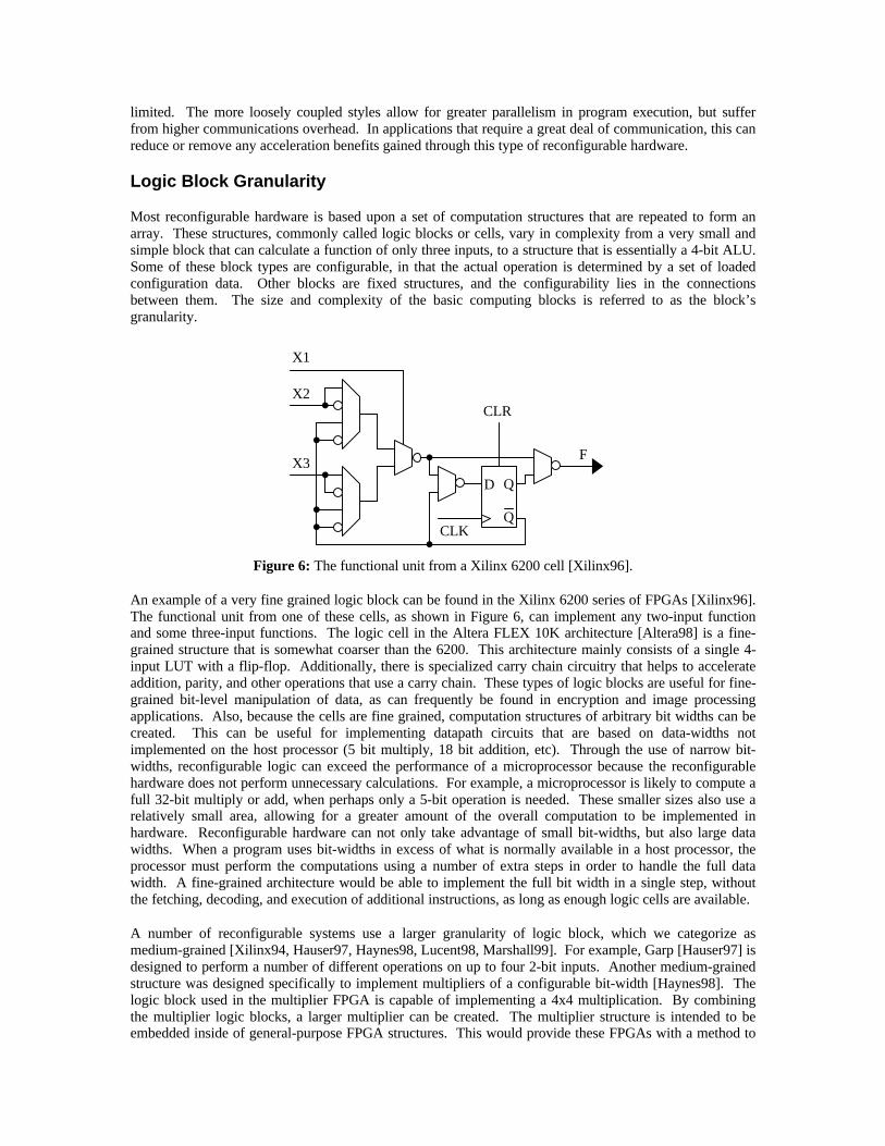
Figure 6: The functional unit from a Xilinx 6200 cell [Xilinx96].
An example of a very fine grained logic block can be found in the Xilinx 6200 series of FPGAs [Xilinx96].The functional unit from one of these cells, as shown in Figure 6, can implement any two-input functionand some three-input functions. The logic cell in the Altera FLEX 10K architecture [Altera98] is a fine-grained structure that is somewhat coarser than the 6200. This architecture mainly consists of a single 4-input LUT with a flip-flop. Additionally, there is specialized carry chain circuitry that helps to accelerateaddition, parity, and other operations that use a carry chain. These types of logic blocks are useful for fine-grained bit-level manipulation of data, as can frequently be found in encryption and image processingapplications. Also, because the cells are fine grained, computation structures of arbitrary bit widths can becreated. This can be useful for implementing datapath circuits that are based on data-widths notimplemented on the host processor (5 bit multiply, 18 bit addition, etc). Through the use of narrow bit-widths, reconfigurable logic can exceed the performance of a microprocessor because the reconfigurablehardware does not perform unnecessary calculations. For example, a microprocessor is likely to compute afull 32-bit multiply or add, when perhaps only a 5-bit operation is needed. These smaller sizes also use arelatively small area, allowing for a greater amount of the overall computation to be implemented inhardware. Reconfigurable hardware can not only take advantage of small bit-widths, but also large datawidths. When a program uses bit-widths in excess of what is normally available in a host processor, theprocessor must perform the computations using a number of extra steps in order to handle the full datawidth. A fine-grained architecture would be able to implement the full bit width in a single step, withoutthe fetching, decoding, and execution of additional instructions, as long as enough logic cells are available.
A number of reconfigurable systems use a larger granularity of logic block, which we categorize asmedium-grained [Xilinx94, Hauser97, Haynes98, Lucent98, Marshall99]. For example, Garp [Hauser97] isdesigned to perform a number of different operations on up to four 2-bit inputs. Another medium-grainedstructure was designed specifically to implement multipliers of a configurable bit-width [Haynes98]. Thelogic block used in the multiplier FPGA is capable of implementing a 4x4 multiplication. By combiningthe multiplier logic blocks, a larger multiplier can be created. The multiplier structure is intended to beembedded inside of general-purpose FPGA structures. This would provide these FPGAs with a method to
perform efficient multiplication, an operation that is considered difficult to map to traditional structures.The CHESS architecture [Marshall99] also operates on 4-bit values, with each of its cells acting as a 4-bitALU.
Medium-grained logic blocks may be used to implement datapath circuits of varying bit widths, similar tothe fine-grained structures. However, with the ability to perform more complex operations of a greaternumber of inputs, this type of structure can be used efficiently to implement a wider variety of operations.For example, finite state machines are frequently too complex to easily map to a reasonable number of fine-grained logic blocks, and are too dependent upon single bit values to be efficiently implemented in a verycoarse-grained architecture.
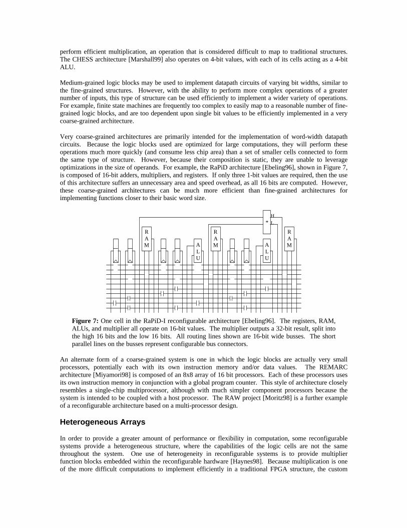
Very coarse-grained architectures are primarily intended for the implementation of word-width datapathcircuits. Because the logic blocks used are optimized for large computations, they will perform theseoperations much more quickly (and consume less chip area) than a set of smaller cells connected to formthe same type of structure. However, because their composition is static, they are unable to leverageoptimizations in the size of operands. For example, the RaPiD architecture [Ebeling96], shown in Figure 7,is composed of 16-bit adders, multipliers, and registers. If only three 1-bit values are required, then the useof this architecture suffers an unnecessary area and speed overhead, as all 16 bits are computed. However,these coarse-grained architectures can be much more efficient than fine-grained architectures forimplementing functions closer to their basic word size.
RAM A
LU
RAM A
LU
RAM
*H
L
Figure 7: One cell in the RaPiD-I reconfigurable architecture [Ebeling96]. The registers, RAM,ALUs, and multiplier all operate on 16-bit values. The multiplier outputs a 32-bit result, split intothe high 16 bits and the low 16 bits. All routing lines shown are 16-bit wide busses. The shortparallel lines on the busses represent configurable bus connectors.
An alternate form of a coarse-grained system is one in which the logic blocks are actually very smallprocessors, potentially each with its own instruction memory and/or data values. The REMARCarchitecture [Miyamori98] is composed of an 8x8 array of 16 bit processors. Each of these processors usesits own instruction memory in conjunction with a global program counter. This style of architecture closelyresembles a single-chip multiprocessor, although with much simpler component processors because thesystem is intended to be coupled with a host processor. The RAW project [Moritz98] is a further exampleof a reconfigurable architecture based on a multi-processor design.
Heterogeneous Arrays
In order to provide a greater amount of performance or flexibility in computation, some reconfigurablesystems provide a heterogeneous structure, where the capabilities of the logic cells are not the samethroughout the system. One use of heterogeneity in reconfigurable systems is to provide multiplierfunction blocks embedded within the reconfigurable hardware [Haynes98]. Because multiplication is oneof the more difficult computations to implement efficiently in a traditional FPGA structure, the custom
multiplication hardware embedded within a reconfigurable array allows a system to perform even thatfunction well.
Another use of heterogeneous structures is to provide embedded memory blocks scattered throughout thereconfigurable hardware. This allows storage of frequently used data and variables, and allows for quickaccess to these values due to the proximity of the memory to the logic blocks that access it. Memorystructures embedded into the reconfigurable fabric come in two forms. The first is simply the use ofavailable LUTs as RAM structures, as can be done in the Xilinx 4000 series [Xilinx94] and Virtex[Xilinx99] FPGAs. Although making these very small blocks into a larger RAM structure introducesoverhead to the memory system, it does provide local, variable width memory structures.
Some architectures include dedicated memory blocks within their array. These memory blocks havegreater performance in large sizes than similar-sized structures built from many small LUTs. While thesestructures are somewhat less flexible than the LUT-based memories, they can also provide somecustomization. For example, the Altera FLEX 10K FPGA [Altera98] provides embedded memories thathave a limited total number of wires, but allow a trade-off between the number of address lines and the databit-width.
When embedded memories are not used for data storage by a particular configuration, the area that theyoccupy does not necessarily have be wasted. By using the address lines of the memory as function inputsand the values stored in the memory as function outputs, logical expressions of a large number of inputscan be emulated [Altera98, Wilton98, Heile99]. In fact, because there may be more than one value outputfrom the memory on a read operation, the memory structure may be able to perform multiple differentcomputations (one for each bit of data output), provided that all necessary inputs appear on the addresslines. In this manner, the embedded RAM behaves the same as a very large LUT. Therefore, embeddedmemory allows a programmer or a synthesis tool to perform a tradeoff between logic and memory usage inorder to achieve higher area efficiency.
Routing Resources
Interconnect resources are provided in an FPGA architecture to interconnect the device’s programmablelogic elements. These resources are usually configurable, where the path of a signal is determined atcompile or run-time rather than fabrication time. This flexible interconnect between logic blocks allows fora wide variety of circuit structures, each with their own interconnect requirements, to be mapped to thereconfigurable hardware. As stated earlier in this paper, the routing for FPGAs is generally island-style,with logic surrounded by routing channels. Within this type of routing architecture, however, there are stillvariations. Some of these differences include the ratio of wires to logic in the system, how long each of thewires should be, and whether they should be connected in a segmented or hierarchical manner.
A step in the design of efficient routing structures for FPGAs and reconfigurable systems therefore involvesexamining the logic vs. routing area tradeoff within reconfigurable architectures. One group has arguedthat the interconnect should constitute a much higher proportion of area in order to allow for successfulrouting under high logic utilization conditions [Takahara98]. However, a high LUT utilization may notnecessarily be the most desirable situation, but rather efficient routing usage may be of more importance[DeHon99]. This is because the routing resources occupy a much larger part of the area of an FPGA thanthe logic resources, and therefore the most area efficient designs will be those that optimize their use of therouting resources rather than the logic resources. The amount of required routing does not grow linearlywith the amount of logic present. Therefore, larger devices require even greater amounts of routing perlogic block than small ones [Trimberger97a].
There are two primary methods to provide both local and global routing resources, as shown in Figure 8.The first is the use of segmented routing. In segmented routing, short wires accommodate localcommunications traffic. These short wires can be connected together using switchboxes to emulate longerwires. Frequently, segmented routing structures also contain longer wires to allow signals to travelefficiently over long distances without passing through a great number of switches. Hierarchical routing

[Aggarwal94, Lai97] is the second method to provide both local and global communication. Routingwithin a group (or cluster) of logic blocks is at the local level, only connecting within that cluster. At theboundaries of these clusters, however, longer wires connect the different clusters together. This ispotentially repeated at a number of levels. The idea behind the use of hierarchical structures is that,provided a good placement has been made onto the hardware, the most communication should be local andonly a limited amount of communication will traverse long distances. Therefore, the wiring is designed tofit this model, with a greater number of local routing wires in a cluster than distance routing wires betweenclusters.
Figure 8: Segmented (left) and hierarchical (right) routing structures. The white boxes are logicblocks, while the dark boxes are connection switches.
Because routing occupies a large part of the area of an FPGA, the type of routing used must be carefullyconsidered. If the wires available are much longer than what is required to route a signal, the excess wirelength is wasted. On the other hand, if the wires available are much shorter than necessary, the signal mustpass through switchboxes that connect the short wires together into a longer wire, or through levels of therouting hierarchy. This induces additional delay and slows the overall operation of the circuit.Furthermore, the switchbox circuitry occupies area that might be better used for additional logic or wires.
There are a few alternatives to the island-style of routing resources. Systems such as RaPiD [Ebeling96]use bus-based routing, where signals are full word-sized in width. This is most common in the one-dimensional type of architecture, as discussed in the next section.
One-dimensional Structures
Most current FPGAs are of the two-dimensional variety, as shown in Figure 9. This allows for a great dealof flexibility, as any signal can be routed on a nearly arbitrary path. However, providing this level ofrouting flexibility requires a great deal of routing area. It also complicates the placement and routingsoftware, as the software must consider a very large number of possibilities.

Figure 9: A traditional two-dimensional island-style routing structure (left) and a one-dimensionalrouting structure (right). The white boxes represent logic elements.
One solution is to use a more one-dimensional style of architecture, also depicted in Figure 9. Here,placement is restricted along one axis. With a more limited set of choices, the placement can be performedmuch more quickly. Routing is also simplified, because it is generally along a single dimension as well,with the other dimension generally only used for calculations requiring a shift operation. One drawback ofthe one-dimensional routing is that if there aren’t enough routing resources in a particular area of a mappedcircuit, routing that circuit becomes actually more difficult than on a two-dimensional array that providesmore alternatives. A number of different reconfigurable systems have been designed in this manner. BothGarp [Hauser97] and Chimaera [Hauck97a] are structures which provide cells that compute a small numberof bit positions, and a row of these cells together computes the full data word. A row can only be used by asingle configuration, making these designs one-dimensional. In this manner, each configuration occupiessome number of complete rows. Although multiple narrow-width computations can fit within a single row,these structures are optimized for word-based computations that occupy the entire row. The NAPAarchitecture [Rupp98] is similar, with a full column of cells acting as the atomic unit for a configuration, asis PipeRench [Cadambi98].
In some systems, the computation blocks in a one-dimensional structure operate on word-width valuesinstead of single bits. Therefore, buses are routed instead of individual values. This also decreases the timerequired for routing, as the bits of a bus can be considered together rather than as separate routes. Asshown in Figure 7, RaPiD [Ebeling96] is basically a one-dimensional design that only includes word-widthprocessing elements. The different computation units are organized in a single dimension along thehorizontal axis. The general flow of information follows this layout, with the major routing busses also laidout in a horizontal manner. Additionally, all routing is of word-sized values, and therefore all routing is ofbuses, not individual wires. A few vertical busses are included in the architecture to allow signals totransfer between busses, or to travel from a bus to a computation node. However, the majority of therouting in this architecture is one-dimensional.
Multi-FPGA Systems
Reconfigurable systems that are composed of multiple FPGA chips interconnected on a single processingboard have additional hardware concerns over single-chip systems. In particular, there is a need for anefficient connection scheme between the chips, as well as to external memory and the system bus. This isto provide for circuits that are too large to fit within a single FPGA, but may be partitioned over themultiple FPGAs available. A number of different interconnection schemes have been explored [Hauck98c,Hauck98d, Khalid99] including meshes and crossbars, as shown in Figure 10. A mesh connects thenearest-neighbors in the array of FPGA chips. This allows for efficient communication between theneighbors, but may require that some signals pass through an FPGA simply to create a connection betweennon-neighbors. Although this can be done, and is quite possible, it uses valuable I/O resources on theFPGA that forms the routing bridge. A crossbar attempts to remove this problem by using special routing-only chips to connect each FPGA potentially to any other FPGA. The inter-chip delays are more uniform,given that a signal travels the exact same “distance” to get from one FPGA to another, regardless of wherethose FPGAs are located. However, a crossbar interconnect does not scale with an increase in the numberof logic FPGAs because of I/O constraints on the chips that are determined at fabrication of the multi-FPGA board. Variants on these two basic topologies attempt to remove some of the problems encountered

in mesh and crossbar topologies [Varghese93, Lewis97, Khalid98]. Because of the need for efficientcommunication between the FPGAs, the determining the inter-chip routing topology is a very importantstep in the design of a multi-FPGA system. More details on multi-FPGA system architectures can be foundelsewhere [Hauck98d].
FPGA
FPGA
FPGA
FPGA
FPGA
FPGA
FPGA
FPGAFPGA FPGA FPGA FPGA
RoutingOnly
RoutingOnly
RoutingOnly
RoutingOnly
Figure 10: Mesh (left) and crossbar (right) interconnect topologies for multi-FPGA systems.
Hardware Summary
The design of reconfigurable hardware varies wildly from system to system. The reconfigurable logic maybe used as a configurable functional unit, or may be a multi-FPGA stand-alone unit. Within thereconfigurable logic itself, the complexity of the core computational units, or logic blocks, vary from verysimple to extremely complex, some implementing a 4-bit ALU or even a 16x16 multiplication. Theseblocks are not required to be uniform throughout the array, as the use of different types of blocks can addhigh-performance functionality in the case of specialized computation circuitry, or expanded storage in thecase of embedded memory blocks. Routing resources also offer a variety of choices, primarily in amount,length, and organization of the wires. Systems have been developed that fit into many different pointswithin this design space, and no true “best” system has yet been declared.
Software
Although reconfigurable hardware has been shown to have significant performance benefits in programexecution, it may be ignored by application programmers unless they are able to easily incorporate its useinto their systems. This requires a software design environment that aids in the creation of configurationsfor the reconfigurable hardware. This software can range from a software assist to manual circuit creationto a complete automated circuit design system. Manual circuit description is a powerful method for thecreation of high-quality circuit designs. However, it requires a great deal of background knowledge of theparticular reconfigurable system employed, as well as a significant amount of design time. On the otherend of the spectrum, an automatic compilation system provides a quick and easy way to program forreconfigurable systems, and therefore makes the use of reconfigurable hardware more accessible to generalapplication programmers.
Both for manual and automatic circuit creation, the design process must proceed through a number ofdistinct phases. Circuit specification is the process of describing the functions that are to be placed on thereconfigurable hardware. This can be done as simply as writing a program in C that represents thefunctionality of the algorithm to be implemented in hardware. On the other hand, this can also be ascomplex as specifying the inputs, outputs, and operation of each basic building block in the reconfigurablesystem. Between these two methods is the specification of the circuit using generic complex components,such as adders and multipliers, which will be mapped to the actual hardware later in the design process.For descriptions in a high level language (HLL), such as C/C++ or Java, or ones using complex buildingblocks, this code must be compiled into a netlist of gate-level components. For the HLL implementationsthis involves generating computational components to perform the arithmetic and logic operations withinthe program, and separate structures to handle the program control, such as loop iterations and branchingoperations. Given a structural description, either generated from a HLL or specified by the user, eachcomplex structure is replaced with a network of the basic gates that perform that function.

Once a detailed gate-level description of the circuit has been created, these structures must be translated tothe actual logic elements of the reconfigurable hardware. This stage is known as technology mapping, andis dependent upon the exact target architecture. For a LUT-based architecture, this stage partitions thecircuit into a number of small sub-functions, each of which can be mapped to a single LUT [Brown92a,Abouzeid93, Vincentelli93, Hwang94, Chang96, Hauck96, Yi96, Chowdhary97, Lin97, Cong98c, Pan98,Togawa98, Cong99]. Some architectures, such as the Xilinx 4000 series [Xilinx94], contain multiple LUTsper logic cell. These LUTs can be used either separately to generate small functions, or together togenerate some wider-input functions [Inuani97, Cong98a]. By taking advantage of multiple LUTs and theinternal routing within a single logic cell, functions with more inputs than can be implemented using asingle LUT can efficiently be mapped into the FPGA architecture. Figure 11 shows one example of a widefunction mapped to a multi-LUT FPGA logic cell.
OUT
ABCD
HG
FE
LUT
LUT
LUTFHBAGAB
FECBAABCDCDBAOUT
)(
)(
++
++=
Figure 11: A wide function implemented with multiple LUTs.
For reconfigurable structures that include embedded memory blocks, the mapping stage may also considerusing these memories as logic units when they are not being used for data storage. The memories act asvery large LUTs, where the number of inputs is equal to the number of address lines. In order to use thesememories as logic, the mapping software must analyze how much of the memory blocks are actually usedas storage in a given mapping. It must then determine which are available in order to implement logic, andwhat part or parts of the circuit are best mapped to the memory [Cong98b, Wilton98].
After the circuit has been mapped, the resulting blocks must be placed onto the reconfigurable hardware.Each of these blocks is assigned to a specific location within the hardware, hopefully close to the otherlogic blocks with which it communicates. As FPGA capacities increase, the placement phase of circuitmapping becomes more and more time consuming. Floorplanning is a technique that can be used toalleviate some of this cost. A floorplanning algorithm first partitions the logic cells into clusters, wherecells with a large amount of communication are grouped together. These clusters are then placed as unitsonto regions of the reconfigurable hardware. Once this global placement is complete, the actual placementalgorithm performs detailed placement of the individual logic blocks within the boundaries assigned to thecluster [Sankar99].
The use of a floorplanning tool is particularly helpful for situations where the circuit structure beingmapped is of a datapath type. Large computational components or macros that are found in datapathcircuits are frequently composed of highly regular logic. These structures are placed as entire units, andtheir component cells are restricted to the floorplanned location [Shi97, Emmert99]. This encourages theplacer to find a very regular placement of these logic cells, resulting in a higher performance layout for thistype of circuit. Another technique for the mapping and placement of datapath elements is to perform bothof these steps simultaneously [Callahan98]. This method also exploits the regularity of the datapathelements to generate mappings and placements both quickly and efficiently.
Floorplanning is also important when dealing with hierarchically structured reconfigurable designs. Inthese architectures the available resources have been grouped by the logic or routing hierarchy of thehardware. Because performance is best when routing is minimized, the cells to be placed should begrouped such that cells which require a great deal of communication or which are on a critical path areplaced together within a logic cluster on the hardware [Krupnova97, Senouci98].

After floorplanning, the individual logic blocks are placed into specific logic cells. One algorithm that iscommonly used is the simulated annealing technique [Shahookar91, Betz97, Sankar99]. This method takesan initial placement of the system, which can be generated randomly, and performs a series of “moves” onthat layout. A move is simply the changing of the location of a single logic cell, or the exchanging oflocations of two logic cells. These moves are attempted one at a time using random target locations at eachiteration. If a move improves the layout, then the layout is changed to reflect that move. If a move isconsidered to be undesirable, then it is only accepted a small percentage of the time. Accepting a few“bad” moves helps to avoid any local minima in the placement space. Placement can also be performeddeterministically [Gehring96], although this searches a smaller area of the placement space for a solution,and therefore may be unable to find a solution which meets performance requirements if a design uses ahigh percentage of the reconfigurable resources.
Finally, the different reconfigurable components comprising the application circuit are connected duringthe routing stage. Particular signals are assigned to specific portions of the routing resources of thereconfigurable hardware. This can become difficult if the placement causes many connected componentsto be placed far from one another, as the signals that travel long distances use more routing resources thanthose that travel shorter ones. A good placement is therefore essential to the routing process. One of thechallenges in routing for FPGAs and reconfigurable systems is that the available routing resources arelimited. In general hardware design, the goal is to minimize the number of routing tracks used in a channelbetween rows of computation units, but the channels can be made as wide as necessary. In reconfigurablesystems, however, the number of available routing tracks is determined at fabrication time, and thereforethe routing software must perform within these boundaries, and concentrate on minimizing congestionwithin the available tracks [Brown92b, Alexander96, Chan97, Lee97, Thakur97, Wu97, Swartz98,Nam99]. Because routing is one of the more time-intensive portions of the design cycle, it can be helpfulto determine if a placed circuit can be routed before actually performing the routing step. This quicklyinforms the designer if changes need to be made to the layout or a larger reconfigurable structure isrequired [Wood97, Swarts98].
Each of the design phases mentioned above may be implemented either manually or automatically usingcompiler tools. The operation of some of these steps are described in greater depth in the followingsections.
Hardware-Software Partitioning
For systems that include both reconfigurable hardware and a traditional microprocessor, the program mustfirst be partitioned into sections to be executed on the reconfigurable hardware and sections to be executedin software on the microprocessor. In general, complex control sequences such as variable loops are moreefficiently implemented in software, while fixed datapath operations may be more optimally executed inhardware.
Most compilers presented for reconfigurable systems generate only the hardware configuration for thesystem, rather than both hardware and software. In some cases, this is because the reconfigurable hardwaremay not be coupled with a host processor, so only a hardware configuration is necessary. For cases wherereconfigurable hardware does operate alongside a host microprocessor, certain compilation methods requirethat the hardware compilation be performed separately from the software compilation, and specialfunctions are called from within the software in order to configure and control the reconfigurable hardware.However, this requires effort on the part of the designer to identify the sections that should be mapped tohardware, and to map these into special hardware functions. In order to make the use of the reconfigurablehardware transparent to the designer, the partitioning and programming of the hardware should occursimultaneously in a single programming environment.
For compilers that manage both the hardware and software aspects of application design, thehardware/software partitioning can be performed either manually, through the use of compiler directives tomark sections of program code for hardware compilation, or automatically by the compiler itself. TheNAPA C language [Gokhale98] provides pragma statements to allow a programmer to specify whether a
section of code is to be executed in software on the Fixed Instruction Processor (FIP), or in hardware on theAdaptive Logic Processor (ALP). [Cardoso99] presents another compiler that requires the user to specify(using information gained through the use of profiling tools) which areas of code to map to thereconfigurable hardware. Automatic partitioners [Chichkov97] [Kress97] use cost functions based uponthe amount of acceleration gained through the execution of a code fragment in hardware to determinewhether the cost of configuration is overcome by the benefits of hardware execution.
Circuit Specification
In order to use the reconfigurable hardware, designers must somehow be able to specify the operation oftheir custom circuits. Before high-level compilation tools are developed for a specific reconfigurablesystem, this is done through hand mapping of the circuit, where the designer specifies the operation of thecomponents in the configurable system directly. Here, the designers utilize the basic building blocks of thereconfigurable system to create the desired circuit. This style of circuit specification is primarily usefulonly when a software front-end for circuit design is unavailable, or for the design of small circuits orcircuits with very high performance requirements. This is due to the great amount of time involved inmanual circuit creation. However, for the circuits that can be reasonably hand-mapped, this providespotentially the smallest and fastest implementation.
Because not all designers can be intimately familiar with every reconfigurable architecture, some designtools abstract the specifics of the target architecture. Creating a circuit using a structural design languageinvolves describing a circuit using building blocks such as gates, flip-flops and latches [Bellows98,Gehring98, Hutchings99]. The compiler then maps these modules to one or more basic components of thearchitecture of the reconfigurable system. Structural VHDL is one example of this type of programming,and commercial tools are available for compiling from this language into vendor-specific FPGAs[Synplicity99].
However, these two methods require that the designer possess either an intimate knowledge of the targetedreconfigurable hardware or a working knowledge of the concepts involved in hardware design. In order toallow a greater number of software developers to take advantage of reconfigurable computing, tools thatallow for behavioral circuit descriptions are being developed. These systems trade some area andperformance quality for greater flexibility and ease of use.
Behavioral circuit design is similar to software design because the designer indicates the steps a hardwaresubsystem must go through in order to perform the desired computation rather than the actual compositionof the circuit. These behavioral descriptions can be either in a generic hardware description language suchas VHDL or Verilog, or a general-purpose high-level language such as C/C++ or Java. The eventual goalof this type of compilation is to allow users to write programs in commonly used languages that compileequally well, without modification, to both a traditional software executable and to an executable whichleverages reconfigurable hardware. Transmogrifier C [Galloway95] allows a subset of the C language tobe used to describe hardware circuits. While multiplication, division, pointers, arrays, and a few other Clanguage specifics are not supported, this system provides a behavioral method of circuit description usinga primitive form of the C language.
Although behavioral description, and HLL description in particular, provides a convenient method for theprogramming of reconfigurable systems, it does suffer from the drawback that it tends to produce largerand slower designs than those generated by a structural description or hand-mapping. Behavioraldescriptions can leave many aspects of the circuit unspecified. For example, a compiler which encounters awhile loop must generate complicated control structures in order to allow for an unspecified number ofiterations. In many HLL implementations, optimizations based upon the bit width of operands cannot beperformed. The compiler is generally unaware of any application-specific limitations on the operand size;it only sees the programmer’s choice of data format in the program. Problems such as these might besolved through additional programmer effort to replace while loops whenever possible with for loops, andto use compiler directives to indicate exact sizes of operands [Galloway95, Gokhale98]. This method ofhardware design falls between structural description and behavioral description in complexity, because

although the programmers do not need to know a great deal about hardware design, they are required tofollow additional guidelines that are not required for software-only implementations.
The NAPA C [Gokhale98] compiler uses a variant of the C language that uses additional constructs tooptimize programs for the reconfigurable hardware. This compiler uses C with additional #pragmacompiler directives to specify certain aspects of the reconfigurable execution. Because this compiler istargeted to the NAPA architecture [Rupp98], which includes both reconfigurable hardware and a RISCcore, many of these #pragma statements specify the partitioning of the program and data between these twostructures. Areas of code that are to be executed on the reconfigurable hardware must be explicitlydelineated. The NAPA C extensions do have the advantage that because they use #pragma statements, thesame code can be compiled for a system that does not include reconfigurable hardware without changingthe program code.
Circuit Libraries
The use of circuit or macro libraries can greatly simplify and speed the design process. By pre-designingcommonly used structures such as adders, multipliers, and counters, circuit creation for configurablesystems becomes largely the assembly of high level components, and only application-specific structuresrequire detailed design. The actual architecture of the reconfigurable device can be abstracted, providedonly library components are used, as these low-level details will already have been encapsulated within thelibrary structures. Although the users of the circuit library may not know the intricacies of the destinationarchitecture, they are still able to make use of architecture-specific optimizations, such as specialized carrychains. This is because designers very familiar with the details of the target architecture create thecomponents within a circuit library. They can take advantage of architecture specifics when creating themodules to make these components faster and smaller than a designer unfamiliar with the architecturelikely would. An added benefit of the architecture abstraction is that the use of library components can alsofacilitate design migration from one architecture to another, because designers are not required to learn anew architecture, but only to indicate the new target for the library components. However, this doesrequire that a circuit library contain implementations for more than one architecture.
One method for using library components is to simply instantiate them within an HDL design [Xilinx97,Altera99]. However, circuit libraries can also be used in general language compilers. The ConfigurationPRofiling tool (CPR) [Cadambi99] compares the data flow graph of the application program to the dataflow graphs of the library macros. If a dataflow representation of a macro matches a portion of theapplication graph, the corresponding macro is used for that part of the configuration. Although thisparticular compiler requires the use of the DIL language [Budiu99], CPR's use of data flow graphs as themain focus of computation allows for future language expansion.
Another benefit of circuit design with library macros is that of fast compilation. Because the librarystructures have been pre-mapped, pre-placed, and pre-routed (at least within the macro boundaries), theactual compile time is reduced to the time required to place the library components and route betweenthem. For example, fast configuration was one of the main motivations for the creation of libraries forcircuit design in the DISC reconfigurable image processing system [Hutchings97].
Circuit Generators
Circuit generators fulfill a role similar to circuit libraries, in that they provide optimized high-levelstructures for use within larger applications. Again, designers are not required to understand the low-leveldetails of particular architectures. However, circuit generators create semi-customized high level structuresautomatically at compile time, as opposed to circuit libraries that only provide static structures. Forexample, a circuit generator can create an adder structure of the exact bit width required by the designer,whereas a circuit library is likely to contain a limited number of adder structures, none of which may be ofthe correct size. Circuit generators are therefore more flexible than circuit libraries because of thecustomization allowed.

Some circuit generators, such as MacGen [Yasar96], are executed at the command line using customdescription files to generate physical design layout data files. Newer circuit generators, however, arefunctions or methods called from high-level language programs. PAM-Blox [Mencer98] is a set of circuitgenerators executed in C++ that generate structures for use with the PCI Pamette reconfigurable processingboard. The circuit generator presented in [Chu98] contains a number of Java classes to allow aprogrammer to generate arbitrarily sized arithmetic and logical components for a circuit. Although theexamples presented in that paper were mapped to a Xilinx 4000 series FPGA, the generator usesarchitecture specific libraries for module generation. The target architecture can therefore be changedthrough the use of a different design library. The Carry Look-Ahead circuit generator described in[Stohmann96] is also retargetable, because it maps to an FPGA logic cell architecture defined by the user.
One drawback of the circuit generators is that they depend on a regular logic and routing structure.Hierarchical routing structures (such as those present in the Xilinx 6200 series [Xilinx96]) and specializedheterogeneous logic blocks are frequently not accounted for. Therefore, some optimized features of aparticular architecture may be unused. For these cases, a circuit macro from a library may provide a morehighly optimized structure than one created with a circuit generator, provided that the library macro fits theneeds of the application.
Partial Evaluation
Functions that are to be implemented on the reconfigurable array should occupy as little area as possible, soas to maximize the number of functions that can be mapped to the hardware. This, combined with theminimization of the delay incurred by each circuit, increases the overall acceleration of the application.Partial evaluation is the process of reducing hardware requirements for a circuit structure throughoptimization based upon known static inputs. Specifically, if an input is known to be constant, that valuecan potentially be propagated through one or more gates in the structure at compile time, and only theportions of a circuit that depend on time-varying inputs need to be mapped to the reconfigurable structure.One example of the usefulness of this operation is that of constant coefficient multipliers. If one input to amultiplier is constant, a multiplier object can be reduced from a general-purpose multiplier to a set ofadditions with static-length shifts between them corresponding to the locations of '1's in the binary constant.This type of reduction leads to a lower area requirement for the circuit, and potentially higher performancedue to fewer gate delays encountered on the critical path. Partial evaluation can also be performed inconjunction with circuit generation, where the constants passed to the generator function are used tosimplify the created hardware circuit [Chu98]. Other examples of this type of optimization for specificalgorithms include the partial evaluation of DES encryption circuits [Leonard97], and the partial evaluationof constant multipliers and fixed polynomial division circuits [Payne97].
Memory Allocation
As with traditional software programs, it may be necessary in reconfigurable computing to allocatememories to hold variables and other data. Off-chip memories may be added to the reconfigurable system.Alternately, if a reconfigurable system includes memory blocks embedded into the reconfigurable logic,these may be used, provided that the storage requirements do not surpass the available embedded memory.If multiple off-chip memories are available to a reconfigurable system, it is desirable to place variablesused in parallel into different memory structures, such that they can be accessed simultaneously.[Gokhale99] discusses a method for partitioning variables into different off-chip memory modules. Whensmaller embedded memory units are used, [Babb99] outlines a method to create larger memories fromsmaller ones, while using techniques to ensure that each smaller memory is close to the computation thatmost requires its contents. As mentioned earlier, the small embedded memories which are not allocated fordata storage may be used to perform logic functions.
Parallelization
One of the benefits of reconfigurable computing is the ability to execute multiple operations in parallel. Incases where circuits are specified using a structural hardware description language, the user specifies all

structures and timing, and therefore either implicitly or explicitly specifies any parallel operation.However, for behavioral and HLL descriptions there are two methods to incorporate parallelism: manualparallelization through special instructions or compiler directives, and automatic parallelization by thecompiler.
RaPiD-B [Cronquist98] is a HLL very similar to C that requires user intervention in order to take advantageof parallelism in the circuit structure. To this end, the user specifies sections of code that are to operate inparallel, and employs signal and wait primitives to allow for synchronization of the different threads ofcomputation. Additionally, this language provides a special loop instruction to generate an innermost looplevel that will be completely unrolled for parallel execution in hardware. Non-inner loops, however, do nothave multiple iterations executing simultaneously. Any loop re-ordering to improve the parallelism of thecircuit must be done by the programmer. On the other hand, NAPA C [Gokhale98] uses both manual andautomatic parallelization when compiling programs into the NAPA architecture. The compiler detects fine-grained parallelism within computations destined for the reconfigurable hardware. However, in order touse parallel threads of execution, the user must specify when the RISC core and the reconfigurablehardware should commence parallel execution and when they should join back into a single thread.
In addition to using the methods described above to exploit both loop and fine-grained parallelism, custompipeline structures can be created in order to overlap sequential operations. [Weinhardt99] presents amethod called pipelined vectorization in which the inner loops of operations are synthesized into generatedcircuits that act as pipelined coprocessors for those sections of code. The DIL compiler [Budiu99] and thePECompiler [Wang97] operate on the entire program instead of just inner loops, generating a control flowgraph based upon the entire program source code. Loop unrolling is used in order to increase the availableparallelism, and the graph is then used to schedule parallel operations in the hardware.
Multi-FPGA System Software
When reconfigurable systems use more than one FPGA to form the complete reconfigurable hardware,there are additional compilation issues to deal with [Hauck96]. The design must first be partitioned into thedifferent FPGA chips [Hauck95, Acock97, Vahid97, Brasen98, Khalid99]. This is generally done byplacing each highly connected portions of a circuit into a single chip. Multi-FPGA systems have a limitednumber of I/O pins that connect the chips together, and therefore their use must be minimized in the overallcircuit mapping. Also, by minimizing the amount of routing required between the FPGAs, the number ofpaths with a high (inter-chip) delay is reduced, and the circuit may have an overall higher performance.Similarly, those sections of the circuit that require a short delay time must be placed upon the same chip.Global placement then determines which of the actual FPGAs in the multi-FPGA system will contain eachof the partitions.
After the circuit has been partitioned into the different FPGA chips, the connections between the chips mustbe routed [Mak97, Ejnioui99]. A global routing algorithm determines at a high level the connectionsbetween the FPGA chips. It first selects a region of output pins on the source FPGA for a given signal,and determines which (if any) routing switches or additional FPGAs the signal must pass through to get tothe destination FPGA. Detailed routing and pin assignment [Kadi94, Hauck97b, Mak97, Ejnioui99] arethen used to assign signals to traces on an existing multi-FPGA board, or to create traces for a multi-FPGAboard that is to be created specifically to implement the given circuit.
Because multi-FPGA systems use inter-chip connections to allow the circuit partitions to communicate,they frequently require a higher proportion of I/O resources vs. logic in each chip than is normally requiredin single-FPGA use. For this reason, some research has focused on methods to allow pins of the FPGAs tobe re-used for multiple signals. This procedure is referred to as Virtual Wires [Babb93, Agarwal95,Selvidge95], and allows for a flexible trade-off between logic and I/O within a given multi-FPGA system.Signals are multiplexed onto a single wire by using multiple virtual clock cycles, one per multiplexedsignal, within a user clock cycle, thus pipelining the communication. In this manner, the I/O requirementsof a circuit can be reduced, while the logic requirements (because of the added circuitry used for themultiplexing) are increased.

Design Testing
After initial compilation and before deploying any application, it needs to be tested for correct operation.For hardware configurations that have been generated from behavioral descriptions, this is similar to thedebugging of a software application. However, structurally and manually created circuits must besimulated and debugged with techniques based upon those from the design of general hardware circuits.For these structures, simulation and debugging are critical not only to ensure proper circuit operation, butalso to prevent possible incorrect connections from causing a short within the circuit, which can damage thereconfigurable hardware.
JHDL [Bellows98, Hutchings99] provides several methods of observing the behavior of a configurationduring simulation. The contents of memory structures within the design can be viewed, modified, or saved.This allows on-the-fly customization of the simulated execution environment of the reconfigurablehardware, as well as a method for examining the computation results. The input and output values ofcircuit structures and substructures can also be viewed either on a generated schematic drawing or with atraditional waveform output. By examining these values, the operation of the circuit can be verified forcorrectness, and conflicts on individual wires can be seen. Other simulation and debugging softwaresystems have also been developed [Gehring96, Lysaght96, McKay99, Vasilko99].
Software Summary
Reconfigurable hardware systems require software compilation tools to allow programmers to harness thebenefits of reconfigurable computing. On one end of the spectrum, circuits for reconfigurable systems canbe designed manually, leveraging all application-specific and architecture-specific optimizations availableto generate a high performance application. However, this requires a great deal of time and effort on thepart of the designer. At the opposite end of the spectrum is fully automatic compilation of a high levellanguage. Using the automatic tools, a software programmer can transparently utilize the reconfigurablehardware without the need for direct intervention. The circuits created using this method, while quicklyand easily created, are generally larger and slower than manually created versions. The actual toolsavailable for compilation onto reconfigurable systems fall at various points within this range, where manyare partially automated but require some amount of manual aid. Circuit designers for reconfigurablesystems therefore face a trade-off between the ease of design and the quality of the final layout.
Run-Time Reconfiguration
Frequently, the areas of a program that can be accelerated through the use of reconfigurable hardware aretoo numerous or complex to be loaded simultaneously onto the available hardware. For these cases, it isbeneficial to be able to swap different configurations in and out of the reconfigurable hardware, as they areneeded during program execution, as shown in Figure 12. This concept is known as run-timereconfiguration.
wwwwww() { wwwwwwwwwwwwwwwwwwwwwwwwwwwwwwwww wwwwwwwwwwwwwwwwwwwwwwwwww wwwwwwwwwwwwwwwww wwwwwwwwwwwwwwwwwwwwwwwwwwwww wwwwwwwwwwwwwwww wwwwwwwwwwwwwwwwwww wwwwwwwwwwwwwwwwwwwwwww wwwwwwwwww w wwwwwwwwwwwwwwwwwwwwwwwwwwwwwwwwwwwwww wwwwwwwwwwwwwwwwwwwwwwwwwwwww wwwwwwwwwwwwwwwwww wwwwwwwwwwwwwwwwwwwwwwwwwwwwww wwwwwwwwwwwwwwwwwwwwww wwwwwwwwwwwwwwwwwwwwwwwwww wwwwwwwwwwwwwwwwwwwwwwwwwwwwwwwwwwwwww w wwwwwwwwwwwwwwwwwwwwwwwwwwwwwwwwww wwwwwwwwwwwwwwwwwwwwwww wwwwwwwwwwwwwwwwwwwwwwwwwwwww wwwwwwwwwwwwwwwwwwwwwwwwwwwwwwwwwwwwwwwwwww wwwwwwwwwwwwwwwwww wwwwwwwwwwwwwwwwwwwwwwwwwwwwwww wwwwwwwwwwwwwwwwwwwwww wwwwwwwwwwwwwwwwwwwwwwwwwwwwwwwwww wwwwwwwwwwwwwwwwwwwwwwwwwwwwwwwwwwwww wwwwwwwwwwwwwwwwwwwwwwww w w wwwwwwwwwwwwwwwwwww wwwwwwwwwwwwwwwwwwwwwwwwwwwwwwwwwwww wwwwwwwwwwwwwwwwwwwwwwwwwwwwww wwwwwwwwwwwwwwwwwwwwwww wwwwwwwwwwwwwwwwwwwwwwwwwwwwwwwwwwwwwwwwww wwwwwwwwww
ReconfigurableFabric
App
licat
ion
Sour
ce C
ode
Figure 12: Some applications have more configurations than can fit in available hardware. In thiscase, we would like to re-program the reconfigurable logic during run-time to allow allconfigurations to be executed in hardware.

Run-time reconfiguration is based upon the concept of virtual hardware. Virtual hardware is similar to theidea of virtual memory. Here, the physical hardware is much smaller than the sum of the resourcesrequired by each of the configurations. Therefore, instead of reducing the number of configurations thatare mapped, we instead swap them in and out of the actual hardware, as they are needed. Because run-timereconfiguration allows more sections of an application to be mapped into hardware than can be fit in a non-run-time reconfigurable system, a greater portion of the program can be accelerated in the run-timereconfigurable systems. This leads to an overall improvement in performance.
There are a few different configuration memory styles that can be used with reconfigurable systems. Asingle context device is a serially programmed chip that requires a complete reconfiguration in order tochange any of the programming bits. A multi-context device has multiple layers of programming bits, eachof which can be active at a different point in time. Devices that can be selectively programmed without acomplete reconfiguration are called partially reconfigurable. These different types of configurationmemory are described in more detail later. An advantage of the multi-context FPGA over a single-contextarchitecture is that it allows for an extremely fast context switch (on the order of nanoseconds), whereas thesingle-context may take milliseconds or more to reprogram. The partially reconfigurable is also moresuited to run-time reconfiguration than the single-context, because small areas of the array can be modifiedwithout requiring that the entire logic array be reprogrammed.
For all of these run-time reconfigurable architectures, there are also a number of compilation issues that arenot encountered in systems that only configure at the beginning of an application. For example, run-timereconfigurable systems are able to optimize based on values that are known only at run-time. Furthermore,compilers must consider the run-time reconfigurability when generating the different circuit mappings, notonly to be aware of the increase in time-multiplexed capacity, but also to schedule reconfigurations so as tominimize the overhead that they incur. These software issues, as well as an overview of methods toperform fast configuration, will be explored in the sections that follow.
Reconfigurable Models
Traditional FPGA structures have been single-context, only allowing one full-chip configuration to beloaded at a time. However, designers of reconfigurable systems have found this style of configuration to betoo limiting and/or slow to efficiently implement run-time reconfiguration. The following discussiondefines the single-context device, and further considers newer FPGA designs (multi-context and partiallyreconfigurable), along with their impact on run-time reconfiguration.
Logic &Routing
Logic &Routing
Single Context
(after reconfiguration)
Incoming configuration
Logic &Routing
Logic &Routing
Partially Reconfigurable
(after reconfiguration)
Incoming configuration
Logic &Routing
Logic &Routing
Multi-Context
(after reconfiguration)
Incoming configuration
Figure 13: The different basic models of reconfigurable computing: single context, multi-context,and partially reconfigurable. Each of these designs is shown performing a reconfiguration.
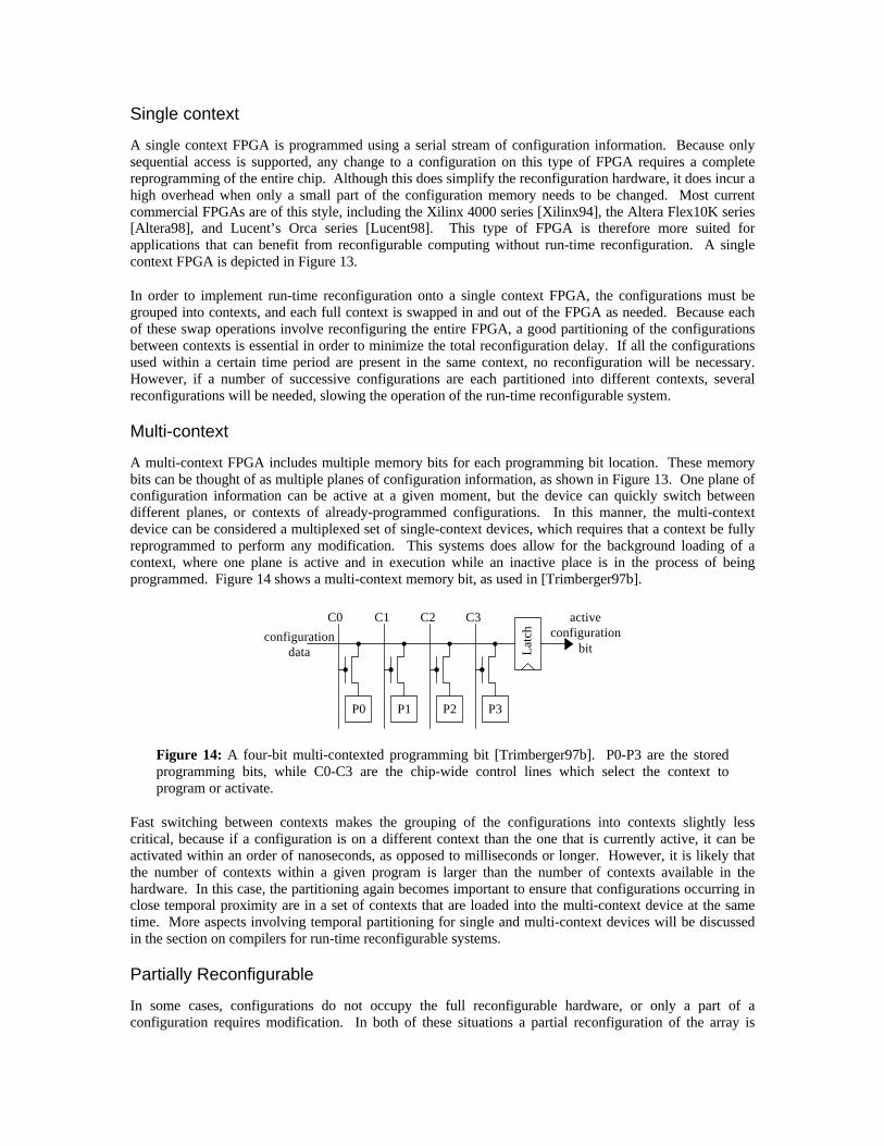
Single context
A single context FPGA is programmed using a serial stream of configuration information. Because onlysequential access is supported, any change to a configuration on this type of FPGA requires a completereprogramming of the entire chip. Although this does simplify the reconfiguration hardware, it does incur ahigh overhead when only a small part of the configuration memory needs to be changed. Most currentcommercial FPGAs are of this style, including the Xilinx 4000 series [Xilinx94], the Altera Flex10K series[Altera98], and Lucent’s Orca series [Lucent98]. This type of FPGA is therefore more suited forapplications that can benefit from reconfigurable computing without run-time reconfiguration. A singlecontext FPGA is depicted in Figure 13.
In order to implement run-time reconfiguration onto a single context FPGA, the configurations must begrouped into contexts, and each full context is swapped in and out of the FPGA as needed. Because eachof these swap operations involve reconfiguring the entire FPGA, a good partitioning of the configurationsbetween contexts is essential in order to minimize the total reconfiguration delay. If all the configurationsused within a certain time period are present in the same context, no reconfiguration will be necessary.However, if a number of successive configurations are each partitioned into different contexts, severalreconfigurations will be needed, slowing the operation of the run-time reconfigurable system.
Multi-context
A multi-context FPGA includes multiple memory bits for each programming bit location. These memorybits can be thought of as multiple planes of configuration information, as shown in Figure 13. One plane ofconfiguration information can be active at a given moment, but the device can quickly switch betweendifferent planes, or contexts of already-programmed configurations. In this manner, the multi-contextdevice can be considered a multiplexed set of single-context devices, which requires that a context be fullyreprogrammed to perform any modification. This systems does allow for the background loading of acontext, where one plane is active and in execution while an inactive place is in the process of beingprogrammed. Figure 14 shows a multi-context memory bit, as used in [Trimberger97b].
P0 P1 P2 P3
Lat
ch
activeconfiguration
bit
C0 C1 C2 C3
configurationdata
Figure 14: A four-bit multi-contexted programming bit [Trimberger97b]. P0-P3 are the storedprogramming bits, while C0-C3 are the chip-wide control lines which select the context toprogram or activate.
Fast switching between contexts makes the grouping of the configurations into contexts slightly lesscritical, because if a configuration is on a different context than the one that is currently active, it can beactivated within an order of nanoseconds, as opposed to milliseconds or longer. However, it is likely thatthe number of contexts within a given program is larger than the number of contexts available in thehardware. In this case, the partitioning again becomes important to ensure that configurations occurring inclose temporal proximity are in a set of contexts that are loaded into the multi-context device at the sametime. More aspects involving temporal partitioning for single and multi-context devices will be discussedin the section on compilers for run-time reconfigurable systems.
Partially Reconfigurable
In some cases, configurations do not occupy the full reconfigurable hardware, or only a part of aconfiguration requires modification. In both of these situations a partial reconfiguration of the array is
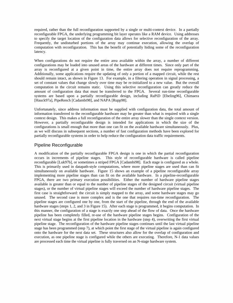
required, rather than the full reconfiguration supported by a single or multi-context device. In a partiallyreconfigurable FPGA, the underlying programming bit layer operates like a RAM device. Using addressesto specify the target location of the configuration data allows for selective reconfiguration of the array.Frequently, the undisturbed portions of the array may continue execution, allowing the overlap ofcomputation with reconfiguration. This has the benefit of potentially hiding some of the reconfigurationlatency.
When configurations do not require the entire area available within the array, a number of differentconfigurations may be loaded into unused areas of the hardware at different times. Since only part of thearray is reconfigured at a given point in time, the entire array does not require reprogramming.Additionally, some applications require the updating of only a portion of a mapped circuit, while the restshould remain intact, as shown in Figure 13. For example, in a filtering operation in signal processing, aset of constant values that change slowly over time may be re-initialized to a new value. But the overallcomputation in the circuit remains static. Using this selective reconfiguration can greatly reduce theamount of configuration data that must be transferred to the FPGA. Several run-time reconfigurablesystems are based upon a partially reconfigurable design, including RaPiD [Ebeling96], Chimaera[Hauck97a], PipeRench [Cadambi98], and NAPA [Rupp98].
Unfortunately, since address information must be supplied with configuration data, the total amount ofinformation transferred to the reconfigurable hardware may be greater than what is required with a singlecontext design. This makes a full reconfiguration of the entire array slower than the single context version.However, a partially reconfigurable design is intended for applications in which the size of theconfigurations is small enough that more than one can fit on the available hardware simultaneously. Plus,as we will discuss in subsequent sections, a number of fast configuration methods have been explored forpartially reconfigurable systems in order to help reduce the configuration data traffic requirements.
Pipeline Reconfigurable
A modification of the partially reconfigurable FPGA design is one in which the partial reconfigurationoccurs in increments of pipeline stages. This style of reconfigurable hardware is called pipelinereconfigurable [Luk97b], or sometimes a striped FPGA [Cadambi98]. Each stage is configured as a whole.This is primarily used in datapath-style computations, where more pipeline stages are used than can fitsimultaneously on available hardware. Figure 15 shows an example of a pipeline reconfigurable arrayimplementing more pipeline stages than can fit on the available hardware. In a pipeline-reconfigurableFPGA, there are two primary execution possibilities. Either the number of hardware pipeline stagesavailable is greater than or equal to the number of pipeline stages of the designed circuit (virtual pipelinestages), or the number of virtual pipeline stages will exceed the number of hardware pipeline stages. Thefirst case is straightforward: the circuit is simply mapped to the array, and some hardware stages may gounused. The second case is more complex and is the one that requires run-time reconfiguration. Thepipeline stages are configured one by one, from the start of the pipeline, through the end of the availablehardware stages (steps 1, 2, and 3 in Figure 15). After each stage is programmed, it begins computation. Inthis manner, the configuration of a stage is exactly one step ahead of the flow of data. Once the hardwarepipeline has been completely filled, re-use of the hardware pipeline stages begins. Configuration of thenext virtual stage begins at the first pipeline location in the hardware (step 4), overwriting the first virtualpipeline stage. The reconfiguration of the hardware pipeline stages continues until the last virtual pipelinestage has been programmed (step 7), at which point the first stage of the virtual pipeline is again configuredonto the hardware for the next data set. These structures also allow for the overlap of configuration andexecution, as one pipeline stage is configured while the others are executing. Therefore, N-1 data valuesare processed each time the virtual pipeline is fully traversed on an N-stage hardware system.
Time
Pipe
line
Stag
es configure 1 execute 1
configure 2 execute 2
configure 3 execute 3
execute 1
execute 2
configure 4 execute 4
execute 3
execute 4
configure 5 execute 5 execute 5
1 2 3 4 5 6 7
configure 1
configure 2
execute 1
Figure 15: A timeline of the configuration and reconfiguration of pipeline stages on a pipelinereconfigurable FPGA. This example shows three physical pipeline stages implementing fivevirtual pipeline stages [Cadambi98].
Communication of Partial Results
During a single program’s execution, configurations are swapped in and out of the reconfigurablehardware. Some of these configurations will likely require access to the results of other configurations.Configurations that are active at different periods in time therefore must be provided with a method tocommunicate with one another. Primarily, this can be done through the use of registers [Ebeling96,Cadambi98, Rupp98, Scalera98], the contents of which can remain intact between reconfigurations. Thisallows one configuration to store a value, and a later configuration to read back that value for use in furthercomputations. An alternative for reconfigurable systems that do not include state-holding devices is towrite the result back to registers or memory external to the reconfigurable array, which is then read back bysuccessive configurations [Hauck97a].
Run-Time Partial Evaluation
One of the advantages that a run-time reconfigurable device has over a system that is only programmed atthe beginning of an application is the ability to perform hardware optimizations based upon valuesdetermined at run-time. Partial evaluation was already discussed in this paper in reference to compilationoptimizations for general reconfigurable systems. Run-time partial evaluation allows for the furtherexploitation of “constants” because the configurations can be modified based not only on completely staticvalues, but also those that change slowly over time [Burns97, Luk97a, Payne97, Wirthlin97, Chu98,McKay99]. This gives reconfigurable circuits the potential to achieve an even higher performance than anASIC, which must retain generality in these situations. The circuit in the reconfigurable system can becustomized to the application at a given time, rather than to the application as a category. For example,where an ASIC may have to include a generic multiplier, a reconfigurable system could instantiate aconstant coefficient multiplier that changes over time. Additionally, partial evaluation can be used inencryption systems [Leonard97]. A key-specific reconfigurable encrypter or decrypter is optimized for theparticular key being used, but retains the ability to use more than one key over the lifetime of the hardware(unlike a key-specialized ASIC) or during actual run-time.
Although partial evaluation can be used to reduce the overall area requirements of a circuit by removingpotentially extraneous hardware within the implementation, occasionally it is preferable to reserve sufficientarea for the largest case, and have all mappings occupy that area. This allows the partially evaluatedportion of a given configuration to be reconfigured, while leaving the remainder of the circuit intact. Forexample, if a constant coefficient multiplier within a larger configuration requires that the constant bechanged, only the area occupied by the multiplier requires reconfiguration. This is true even if the newconstant coefficient multiplier is a larger structure than the previous one, because the reserved area for it isbased upon the largest possibility [McKay99]. Although partial evaluation does not minimize the areaoccupied by the circuit in this case, the speed of configuration is improved by making the multiplier amodular replaceable component. Additionally, this method retains the speed benefits of partialreconfiguration because it still minimizes the logic and routing actually used to implement the structure.

Compilation
For some reconfigurable systems a configuration requires programming the reconfigurable hardware onlyat the start of its execution. On the other hand, in a run-time reconfigurable system the circuits loaded onthe hardware change over time. If the user must specify by hand the loading and execution of the circuitsin the reconfigurable hardware, then the compilers must include methods to indicate these operations.JHDL [Bellows98, Hutchings99] is one such compiler. It provides for the instantiation of configurationsthrough the use of Java constructors, and the removal of the circuits from the hardware by using adestructor on the circuit objects. This allows the programmer to indicate exactly the loading pattern of theconfigurations.
Alternately, the use of the run-time reconfigurable hardware can be automated by the compiler. For asingle-context or multi-context device, configurations must be temporally partitioned into a number ofdifferent full contexts of configuration information. This involves determining which configurations arelikely to be used near in time to one another, and which configurations are able to fit together onto thereconfigurable hardware. Ideally, the number of re-configurations that are to be performed is minimized.By reducing the number of reconfigurations, the proportion of time spent in reconfiguration compared tothe time spent in useful computation is reduced. This issue is discussed in more depth in later sections.
The problem of forming and scheduling single and multi-configuration contexts for use in single-contextand multi-context FPGA designs has been discussed by a number of groups [Chang98, Trimberger98,Liu99, Purna99]. In particular, a single circuit that is too large to fit within the reconfigurable hardwaremay be partitioned over time to form a sequential set of configurations. This involves examining thecontrol flow graph of the circuit and dividing the circuit into distinct computation nodes. The nodes canthen be grouped together within contexts, based upon their proximity to one another within the flow controlgraph. If possible, those configurations that are used in quick succession will be placed within the samegroup. These groups are finally mapped into full contexts, to be loaded into the reconfigurable hardware atruntime.
For partially reconfigurable designs, the compiler must determine the optimal placement to preventconfigurations that are used together in close temporal proximity from occupying the same resources.Again, through minimizing the number of reconfigurations, the overall performance of the system isincreased, as configuration is a slow process [Li00]. An alternative approach, which allows the finalplacement of a configuration to be determined at run-time, is also discussed in the next section.
Fast Configuration
Because run-time reconfigurable systems involve reconfiguration during program execution, thereconfiguration must be done as efficiently and as quickly as possible. This is in order to ensure that theoverhead of the reconfiguration does not eclipse the benefit gained by hardware acceleration. Stallingexecution of either the host processor or the reconfigurable hardware because of configuration is clearlyundesirable. In the DISC II system, from 25% [Wirthlin96] to 71% [Wirthlin95] of execution time is spentin reconfiguration, while in the UCLA ATR work this figure can rise to over 98.5% [Smith99]. If thedelays caused by reconfiguration are reduced, performance can be greatly increased. Therefore, fastconfiguration is an important area of research for run-time reconfigurable systems.
There are a number of different tactics for reducing the configuration overhead. First, loading of theconfigurations can be timed such that the configuration overlaps as much as possible with the execution ofinstructions by the host processor. Second, compression techniques can be introduced to decrease theamount of configuration data that must be transferred to the system. Third, the number of times areconfiguration is necessary can be reduced through hardware optimizations that help prevent programmedconfigurations that will be reused from being unnecessarily replaced by incoming configurations. Finally,the actual process of transferring the data from the host processor to the reconfigurable hardware can bemodified to include a configuration cache, which would provide a faster reconfiguration.

Configuration Prefetching
Performance is improved when the actual configuration of the hardware is overlapped with computationsperformed by the host processor, because programming the reconfigurable hardware requires frommilliseconds to seconds to accomplish. Overlapping configuration and execution prevents the hostprocessor from stalling while it is waiting for the configuration to finish, and hides the configuration timefrom the program execution. Configuration pre-fetching [Hauck98b] attempts to leverage this overlap bydetermining when to initiate reconfiguration of the hardware in order to maximize overlap with usefulcomputation on the host processor. It also seeks to minimize the chance that a configuration will be pre-fetched falsely, overwriting the configuration that is actually used next.
Configuration Compression
Unfortunately, there will always be cases in which the configuration overheads cannot be successfullyhidden using a pre-fetching technique. This can occur when a conditional branch occurs immediatelybefore the use of a configuration, potentially making a 100% correct pre-fetch prediction impossible, orwhen multiple configurations or contexts must be loaded in quick succession. In these cases, the delayincurred is minimized when the amount of data transferred from the host processor to the reconfigurablearray is minimized. Configuration compression can be used to compact this configuration information[Hauck98a, Hauck99, Li99].
One form of configuration compression has already been implemented in a commercial system. The Xilinx6200 series of FPGA [Xilinx96] contains wildcarding hardware, which provides a method to programmultiple logic cells with a single address and data value. This is accomplished by setting a special registerto indicate which of the address bits should behave as "don’t-care" values, resolving to multiple addressesfor configuration. For example, suppose two configuration addresses, 00010 and 00110, are both are to beprogrammed with the same value. By setting the wildcard register to 00100, the address value sent isinterpreted as 00X10 and both these locations are programmed using either of the two addresses above in asingle operation. [Hauck98a] discusses the benefits of this hardware, while [Li99] covers a potentialextension to the concept, where “don’t care” values in the configuration stream can be used to allow areaswith similar but not identical configuration data values to also be programmed simultaneously.
Within partially reconfigurable systems there is an added potential to effectively compress the amount ofdata sent to the reconfigurable hardware. A configuration can possibly re-use configuration informationalready present on the array, such that only the areas differing in configuration values must be re-programmed. Therefore, configuration time can be reduced through the identification of these commoncomponents and the calculation of the incremental configurations that must be loaded [Luk97a, Shirazi98].
Alternately, similar operations can be grouped together to form a single configuration which contains extracontrol circuitry in order to implement the various functions within the group [Kastrup99]. By creatinglarger configurations out of groups of smaller configurations, the configuration overhead of partialreconfiguration is reduced because more operations can be present on chip simultaneously. However, thereare some area and execution penalties imposed by this method, creating a tradeoff between reducedreconfiguration overhead and faster execution with a smaller area.
Relocation and Defragmentation in Partially Reconfigurable Systems
Partially reconfigurable systems have the advantage over single-context systems in that they allow a newconfiguration to be written to the programmable logic while the configurations not occupying that samearea remain intact and available for future use. Because these configurations will not have to bereconfigured onto the array, and because the programming of a single configuration can require the transferof far less configuration data than the programming of an entire context, a partially reconfigurable systemcan incur less configuration overhead than a single-context FPGA. However, inefficiencies can arise if twopartial configurations have been placed to overlapping physical locations on the FPGA. If theseconfigurations are repeatedly used one after another, they must be swapped in and out of the array eachtime. This type of conflict could negate much of the benefit achieved by partially reconfigurable systems.

A better solution to this problem is to allow the final placement of the configurations to occur at run-time,allowing for run-time relocation of those configurations [Compton00, Li00]. Using relocation, a newconfiguration may be placed onto the reconfigurable array where it will cause minimum conflict with otherneeded configurations already present on the hardware. A number of different systems support run-timerelocation, including Chimaera [Hauck97a], Garp [Hauser97], and PipeRench [Cadambi98].
Even with relocation, partially reconfigurable hardware can still suffer from some placement conflicts thatcould be avoided by using an additional hardware optimization. Over time, as a partially reconfigurabledevice loads and unloads configurations, the location of the unoccupied area on the array is likely tobecome fragmented, similar to what occurs in memory systems when RAM is allocated and deallocated.There may be enough empty area on the device to hold an incoming configuration, but it may be distributedthroughout the array. A configuration normally requires a contiguous region of the chip, so it would haveto overwrite a portion of a valid configuration in order to be placed onto the reconfigurable hardware. Asystem that incorporates the ability to perform defragmentation of the reconfigurable array, however, wouldbe able to consolidate the unused area by moving valid configurations to new locations [Diessel97,Compton00]. This area can then be used by incoming configurations, potentially without overwriting anyof the moved configurations.
Configuration Caching
Because a great deal of the delay caused by configuration is due to the distance between the host processorand the reconfigurable hardware, as well the reading of the configuration data from a file or main memory,a configuration cache can potentially reduce the costs of reconfiguration [Deshpande99]. By storing theconfigurations in fast memory near to the reconfigurable array, the data transfer during reconfiguration isaccelerated, and the overall time required is reduced.
Potential Problems with RTR
Partial reconfiguration involves selectively programming portions of the reconfigurable array. However, inmany architectures there are some routing resources which traverse long distances, and may traverse areasallocated to different configurations. Care must be taken such that different configurations do not attemptto drive to these wires simultaneously, as multiple drivers to a wire can potentially damage the hardware.Therefore, systems such as the Xilinx 6200 [Xilinx96] and Chimaera [Hauck97a] have specially designedrouting resources that prevent multiple drivers.
An additional difficulty in using run-time reconfigurable systems occurs when the host processor runsmultiple threads or processes [Chien99, Jean99]. These threads or processes may each have their own setsof configurations that are to be mapped to the reconfigurable hardware. Issues such as the correct use ofmemory protection and virtual memory must be considered during memory accesses by the reconfigurablehardware. Another problem can occur when one thread or process configures the hardware, which is thenreconfigured by a different thread or process. Threads and processes must be prevented from incorrectlycalling hardware functions that no longer appear on the reconfigurable hardware. This requires that thestate of the reconfigurable hardware be set to “dirty” on a main processor context switch, or re-loaded withthe correct configuration context.
Partially reconfigurable systems must also protect against inter-process or inter-thread conflicts within thearray. Even if each application has ensured that their own configurations can safely co-exist, a combinationof configurations from different applications re-introduces the possibility of inadvertently causing anelectrical short within the reconfigurable hardware. This particular issue can be solved through the use ofan architecture that does not have “bad” configurations, such as the 6200 series [Xilinx96] and Chimaera[Hauck97a]. The potential for this type of conflict also introduces the possibility of extremely destructiveconfigurations that can destroy the system’s underlying hardware.

Run-Time Reconfiguration Summary
We have discussed the benefits of using run-time reconfiguration to increase the benefits gained throughreconfigurable computing. Different configurations may be used at different phases of a program’sexecution, customizing the hardware not only for the application, but also for the different stages of theapplication. Run-time reconfiguration also allows configurations larger than the available reconfigurablehardware to be implemented, as these circuits can be split into several smaller ones that are used insuccession. Because of the delays associated with configuration, this style of computing requires thatreconfiguration be performed in a very efficient manner. The multi-context and the partially reconfigurableFPGA are both designed to improve the time required for reconfiguration. Hardware optimizations, such aswildcarding, run-time relocation, and defragmentation, further decrease configuration overhead in apartially reconfigurable design. Software techniques to enable fast configuration, including pre-fetching,compression, and incremental configuration calculation were also discussed.
Conclusion
Reconfigurable computing is becoming an important part of research in computer architectures andsoftware systems. By placing the computationally intense portions of an application onto thereconfigurable hardware, that application can be greatly accelerated. This is because reconfigurablecomputing combines the benefits of both software and ASIC implementations. Like software, the mappedcircuit is flexible, and can be changed over the lifetime of the system or even the lifetime of the application.Similar to an ASIC, reconfigurable systems provide a method to map circuits into hardware, achieving fargreater performance than software as a result of bypassing the fetch-decode-execute cycle of traditionalmicroprocessors, and parallel execution of multiple operations.
Reconfigurable hardware systems come in many forms, from a configurable functional unit integrateddirectly into a CPU, to a reconfigurable co-processor coupled with a host microprocessor, to a multi-FPGAstand-alone unit. The level of coupling, granularity of computation structures, and form of routingresources are all key points in the design of reconfigurable systems. The use of heterogeneous structurescan also greatly add to the overall performance of the final design.
Compilation tools for reconfigurable systems range from simple tools that aid in the manual design andplacement of circuits, to fully automatic design suites that use program code written in a high-levellanguage to generate circuits and the controlling software. The variety of tools available allows designersto choose between manual and automatic circuit creation for any or all of the design steps. Althoughautomatic tools greatly simplify the design process, manual creation is still important for performance-driven applications. Circuit libraries and circuit generators are additional software tools that enabledesigners to quickly create efficient designs. These tools attempt to aid the designer in gaining the benefitsof manual design without entirely sacrificing the ease of automatic circuit creation.
Finally, run-time reconfiguration provides a method to accelerate a greater portion of a given application byallowing the configuration of the hardware to change over time. Apart from the benefits of added capacitythrough the use of virtual hardware, run-time reconfiguration also allows for circuits to be optimized basedon tun-time conditions. In this manner, performance of a reconfigurable system can approach or evensurpass that of an ASIC.
Reconfigurable computing systems have shown the ability to greatly accelerate program execution,providing a high-performance alternative to software-only implementations. However, no one hardwaredesign has emerged as the clear pinnacle of reconfigurable design. Although general-purpose FPGAstructures have standardized into LUT-based architectures, groups designing hardware for reconfigurablecomputing are currently also exploring the use of heterogeneous structures and word-width computationalelements. Those designing compiler systems face the task of improving automatic design tools to the pointwhere they may achieve mappings comparable to manual design for even high-performance applications.Within both of these research categories lies the additional topic of run-time reconfiguration. While somework has been done in this field as well, research must continue in order to be able to perform faster and
more efficient reconfiguration. Further study into each of these topics is necessary in order to harness thefull potential of reconfigurable computing.
Acknowledgments
This research was funded in part by DARPA contracts DABT63-97-C-0035 and F30602-98-0144, and agrant from Motorola, Inc. Katherine Compton was supported by an NSF Fellowship.
References
[Abouzeid93] P. Abouzeid, B. Babba, M. C. de Paulet, G. Saucier, “Input-Driven Partitioning Methodsand Application to Synthesis on Table-Lookup-Based FPGA’s”, IEEE Transactions onComputer-Aided Design of Integrated Circuits and Systems, Vol. 12, No. 7, July 1993.
[Acock97] S. J. B. Acock, K. R. Dimond, “Automatic Mapping of Algorithms onto Multiple FPGA-SRAM Modules”, Lecture Notes in Computer Science 1304—Field-Programmable Logicand Applications. W. Luk, P. Y. K. Cheung, M. Glesner, Eds. Berlin, Germany:Springer-Verlag, pp. 255-264, 1997.
[Agarwal95] A. Agarwal, “VirtualWires: A Technology for Massive Multi-FPGA Systems”,http://www.ikos.com/products/virtualwires.ps, 1995.
[Aggarwal94] A. Aggarwal, D. Lewis, “Routing Architectures for Hierarchical Field ProgrammableGate Arrays”, Proceedings IEEE International Conference on Computer Design, pp.475-478, 1994.
[Alexander96] M. J. Alexander, G. Robins, “New Performance-Driven FPGA Routing Algorithms”,IEEE Transactions on CAD of Integrated Circuits and Systems, Vol. 15, No. 12, pp.1505-1517, December 1996.
[Altera98] Data Book, San Jose, CA: Altera Corporation, 1998.
[Altera99] “Altera MegaCore Functions”, http://www.altera.com/html/tools/megacore.html, SanJose, CA: Altera Corporation, 1999.
[Annapolis98] Wildfire Reference Manual, Annapolis, Maryland: Annapolis Microsystems, Inc., 1998.
[Babb93] J. Babb, R. Tessier, A. Agarwal, “Virtual Wires: Overcoming Pin Limitations in FPGA-based Logic Emulators”, IEEE Workshop on FPGAs for Custom Computing Machines,pp. 142-151, 1993.
[Babb99] J. Babb, M. Rinard, C. A. Moritz, W. Lee, M. Frank, R. Barua, S. Amarasinghe,"Parallelizing Applications into Silicon", IEEE Symposium on Field-ProgrammableCustom Computing Machines, 1999.
[Bellows98] P. Bellows, B. Hutchings, "JHDL - An HDL for Reconfigurable Systems", IEEESymposium on Field-Programmable Custom Computing Machines, 1998.
[Betz97] V. Betz, J. Rose, “VPR: A New Packing, Placement and Routing Tool for FPGAResearch”, Lecture Notes in Computer Science 1304—Field-Programmable Logic andApplications. W. Luk, P. Y. K. Cheung, M. Glesner, Eds. Berlin, Germany: Springer-Verlag, pp. 213-222, 1997.
[Betz99] V. Betz, J. Rose, “FPGA Routing Architecture: Segmentation and Buffering to OptimizeSpeed and Density”, ACM/SIGDA International Symposium on FPGAs, pp. 59-68, 1999.
[Brasen98] D. R. Brasen, G. Saucier, “Using Cone Structures for Circuit Partitioning into FPGAPackages”, IEEE Transactions on CAD of Integrated Circuits and Systems, Vol. 17, No.7, pp. 592-600, July 1998.
[Brown92a] S. D. Brown, R. J. Francis, J. Rose, Z. G. Vranesic, Field-Programmable Gate Arrays,Boston, Mass: Kluwer Academic Publishers, 1992.
[Brown92b] S. Brown, J. Rose, Z. G. Vranesic, “A Detailed Router for Field-Programmable GateArrays”, IEEE Transactions on Computer-Aided Design, Vol. 11, No. 5, pp. 620-628,May 1992.
[Budiu99] M. Budiu, S. C. Goldstein, "Fast Compilation for Pipelined Reconfigurable Fabrics",ACM/SIGDA International Symposium on FPGAs, pp. 195-205, 1999.
[Burns97] J. Burns, A. Donlin, J. Hogg, S. Singh, M. de Wit, “A Dynamic Reconfiguration Run-Time System”, IEEE Symposium on Field-Programmable Custom Computing Machines,1997.
[Cadambi98] S. Cadambi, J. Weener, S. C. Goldstein, H. Schmit, D. E. Thomas, “Managing Pipeline-Reconfigurable FPGAs”, ACM/SIGDA International Symposium on FPGAs, pp. 55-64,1998.
[Cadambi99] S. Cadambi, S. C. Goldstein, "CPR: A Configuration Profiling Tool", IEEE Symposiumon Field-Programmable Custom Computing Machines, 1999.
[Callahan98] T. J. Callahan, P. Chong, A. DeHon, J. Wawrzynek, “Fast Module Mapping andPlacement for Datapaths in FPGAs”, ACM/SIGDA International Symposium on FPGAs,pp. 123-132, 1998.
[Cardoso99] J. M. P. Cardoso, H. C. Neto, "Macro-Based Hardware Compilation of Java™ Bytecodesinto a Dynamic Reconfigurable Computing System", IEEE Symposium on Field-Programmable Custom Computing Machines, 1999.
[Chan97] P. K. Chan, M. D. F. Schalg, “Acceleration of an FPGA Router”, IEEE Symposium onField-Programmable Custom Computing Machines, 1997.
[Chang96] S.-C. Chang, M. Marek-Sadowska, T. T. Hwang, “Technology Mapping for TLUFPGA’s Based on Decomposition of Binary Decision Diagrams”, IEEE Transactions onCAD of Integrated Circuits and Systems, Vol. 15, No. 10, pp. 1226-1248, October 1996.

[Chang98] D. Chang, M. Marek-Sadowska, “Partitioning Sequential Circuits on DynamicallyReconfigurable FPGAs”, ACM/SIGDA International Symposium on FPGAs, pp. 161-167,1998.
[Chichkov97] A. V. Chichkov, C. B. Almeida, “An Hardware/Software Partitioning Algorithm forCustom Computing Machines”, Lecture Notes in Computer Science 1304—Field-Programmable Logic and Applications. W. Luk, P. Y. K. Cheung, M. Glesner, Eds.Berlin, Germany: Springer-Verlag, pp. 274-283, 1997.
[Chien99] A. A. Chien, J. H. Byun, “Safe and Protected Execution for the Morph/AMRMReconfigurable Processor”, IEEE Symposium on Field-Programmable CustomComputing Machines, 1999.
[Chowdhary97] A. Chowdhary, J. P. Hayes, “General Modeling and Technology-Mapping Technique forLUT-based FPGAs”, ACM/SIGDA International Symposium on FPGAs, pp. 43-49, 1997.
[Chu98] M. Chu, N. Weaver, K. Sulimma, A. DeHon, J. Wawrzynek, "Object Oriented Circuit-Generators in Java", IEEE Symposium on Field-Programmable Custom ComputingMachines, 1998.
[Compton00] K. Compton, J. Cooley, S. Knol, S. Hauck, “FPGA Hardware Support for ConfigurationRelocation and Defragmentation”, in preparation for IEEE Symposium on Field-Programmable Custom Computing Machines, 2000.
[Cong98a] J. Cong, Y-Y. Hwang, “Boolean Matching for Complex PLBs in LUT-based FPGAs withApplication to Architecture Evaluation”, ACM/SIGDA International Symposium onFPGAs, pp. 27-34, 1998.
[Cong98b] J. Cong, S. Xu, “Technology Mapping for FPGAs with Embedded Memory Blocks”,ACM/SIGDA International Symposium on FPGAs, pp. 179-188, 1998.
[Cong98c] J. Cong, C. Wu, “An Efficient Algorithm for Performance-Optimal FPGA TechnologyMapping with Retiming”, IEEE Transactions on CAD of Integrated Circuits andSystems, Vol. 17, No. 9, pp. 738-748, September 1998.
[Cong99] J. Cong, C. Wu, Y. Ding, “Cut Ranking and Pruning Enabling A General And EfficientFPGA Mapping Solution”, ACM/SIGDA International Symposium on FPGAs, pp. 29-35,1999.
[Cronquist98] D. C. Cronquist, P. Franklin, S. G. Berg, C. Ebeling, "Specifying and CompilingApplications for RaPiD", IEEE Symposium on Field-Programmable Custom ComputingMachines, 1998.
[DeHon99] A. DeHon, “Balancing Interconnect and Computation in a Reconfigurable ComputingArray (or, why you don’t really want 100% LUT utilization)”, ACM/SIGDA InternationalSymposium on FPGAs, pp. 69-78, 1999.
[Deshpande99] D. Deshpande, A. K. Somani, A. Tyagi, “Configuration Caching Vs Data Caching forStriped FPGAs”, ACM/SIGDA International Symposium on FPGAs, pp. 206-214, 1999.

[Diessel97] O. Diessel, H. ElGindy, “Run-Time Compaction of FPGA Designs”, Lecture Notes inComputer Science 1304—Field-Programmable Logic and Applications. W. Luk, P. Y.K. Cheung, M. Glesner, Eds. Berlin, Germany: Springer-Verlag, pp. 131-140, 1997.
[Ebeling96] C. Ebeling, D. C. Cronquist, P. Franklin, “RaPiD – Reconfigurable Pipelined Datapath”,Lecture Notes in Computer Science 1142—Field-Programmable Logic: SmartApplications, New Paradigms and Compilers. R. W. Hartenstein, M. Glesner, Eds.Berlin, Germany: Springer-Verlag, pp. 126-135, 1996.
[Ejnioui99] A. Ejnioui, N. Ranganathan, “Multi-Terminal Net Routing for Partial Crossbar-BasedMulti-FPGA Systems”, ACM/SIGDA International Symposium on FPGAs, pp. 176-184,1999.
[Emmert99] J. M. Emmert, D. Bhatia, “A Methodology for Fast FPGA Floorplanning”, ACM/SIGDAInternational Symposium on FPGAs, pp. 47-56, 1999.
[Galloway95] D. Galloway, “The Transmogrifier C Hardware Description Language and Compiler forFPGAs”, IEEE Symposium on FPGAs for Custom Computing Machines, pp. 136-144,1995.
[Gehring96] S. Gehring, S. Ludwig, “The Trianus System and Its Application to Custom Computing”,Lecture Notes in Computer Science 1142—Field-Programmable Logic: SmartApplications, New Paradigms and Compilers. R. W. Hartenstein, M. Glesner, Eds.Berlin, Germany: Springer-Verlag, pp. 176-184, 1996.
[Gehring98] S. W. Gehring, S. H-M. Ludwig, “Fast Integrated Tools for Circuit Design with FPGAs”,ACM/SIGDA International Symposium on FPGAs, pp. 133-139, 1998.
[Gokhale98] M. B. Gokhale, J. M. Stone, "NAPA C: Compiling for a Hybrid RISC/FPGAArchitecture", IEEE Symposium on Field-Programmable Custom Computing Machines,1998.
[Gokhale99] M. B. Gokhale, J. M. Stone, "Automatic Allocation of Arrays to Memories in FPGAProcessors With Multiple Memory Banks", IEEE Symposium on Field-ProgrammableCustom Computing Machines, 1999.
[Hauck95] S. Hauck, Multi-FPGA Systems, Ph.D. Thesis, University of Washington, Dept. ofC.S.&E., September 1995.
[Hauck96] S. Hauck, A. Agarwal, “Software Technologies for Reconfigurable Systems”,Northwestern University, Dept. of ECE Technical Report, 1996.
[Hauck97a] S. Hauck, T. W. Fry, M. M. Hosler, J. P. Kao, "The Chimaera Reconfigurable FunctionalUnit", IEEE Symposium on Field-Programmable Custom Computing Machines, 1997.
[Hauck97b] S. Hauck, G. Borriello, "Pin Assignment for Multi-FPGA Systems", IEEE Transactionson Computer-Aided Design of Integrated Circuits and Systems, Vol. 16, No. 9, pp. 956-964, September, 1997.
[Hauck98a] S. Hauck, Z. Li, E. Schwabe, "Configuration Compression for the Xilinx XC6200FPGA", IEEE Symposium on Field-Programmable Custom Computing Machines, 1998.
[Hauck98b] S. Hauck, “Configuration Prefetch for Single Context Reconfigurable Coprocessors”,ACM/SIGDA International Symposium on FPGAs, pp. 65-74, 1998.
[Hauck98c] S. Hauck, G. Borriello, C. Ebeling "Mesh Routing Topologies for Multi-FPGA Systems",IEEE Transactions on VLSI Systems, Vol. 6, No. 3, pp. 400-408, September 1998.
[Hauck98d] S. Hauck, “The Roles of FPGAs in Reprogrammable Systems” Proceedings of the IEEE,Vol. 86, No. 4, pp. 615-638, April 1998.
[Hauck99] S. Hauck, W. D. Wilson, “Runlength Compression Techniques for FPGAConfigurations”, Northwestern University, Dept. of ECE Technical Report, 1999.
[Hauser97] J. R. Hauser, J. Wawrzynek, "Garp: A MIPS Processor with a ReconfigurableCoprocessor", IEEE Symposium on Field-Programmable Custom Computing Machines,1997.
[Haynes98] S. D. Haynes, P. Y. K. Cheung, "A Reconfigurable Multiplier Array For Video ImageProcessing Tasks, Suitable for Embedding In An FPGA Structure", IEEE Symposium onField-Programmable Custom Computing Machines, 1998.
[Heile99] F. Heile, A. Leaver, “Hybrid Product Term and LUT Based Architectures UsingEmbedded Memory Blocks”, ACM/SIGDA International Symposium on FPGAs, pp. 13-16, 1999.
[Hutchings97] B. L. Hutchings, “Exploiting Reconfigurability Through Domain-Specific Systems”,Lecture Notes in Computer Science 1304—Field-Programmable Logic and Applications.W. Luk, P. Y. K. Cheung, M. Glesner, Eds. Berlin, Germany: Springer-Verlag, pp. 193-202, 1997.
[Hutchings99] B. Hutchings, P. Bellows, J. Hawkins, S. Hemmert, B. Nelson, M. Rytting, "A CADSuite for High-Performance FPGA Design", IEEE Symposium on Field-ProgrammableCustom Computing Machines, 1999.
[Hwang94] T.-T. Hwang, R. M. Owens, M. J. Irwin, K. H. Wang, “Logic Synthesis for Field-Programmable Gate Arrays”, IEEE Transactions on Computer-Aided Design ofIntegrated Circuits and Systems, Vol. 13, No. 10, October 1994.
[Inuani97] M. K. Inuani, J. Saul, “Technology Mapping of Heterogeneous LUT-Based FPGAs”,Lecture Notes in Computer Science 1304—Field-Programmable Logic and Applications.W. Luk, P. Y. K. Cheung, M. Glesner, Eds. Berlin, Germany: Springer-Verlag, pp. 223-234, 1997.
[Jean99] J. S. N. Jean, K. Tomko, V. Yavagal, J. Shah, R. Cook, “Dynamic Reconfiguration toSupport Concurrent Applications”, IEEE Transactions on Computers, Vol. 48, No. 6, pp.591-602, June 1999.

[Kadi94] M. Slimane-Kadi, D. Brasen, G. Saucier, “A Fast-FPGA Prototyping System That UsesInexpensive High-Performance FPIC”, ACM/SIGDA Workshop on Field-ProgrammableGate Arrays, 1994.
[Kastrup99] B. Kastrup, A. Bink, J. Hoogerbrugge, "ConCISe: A Compiler-Driven CPLD-BasedInstruction Set Accelerator", IEEE Symposium on Field-Programmable CustomComputing Machines, 1999.
[Khalid98] M. A. S. Khalid, J. Rose, “A Hybrid Complete-Graph Partial-Crossbar RoutingArchitecture for Multi-FPGA Systems”, ACM/SIGDA International Symposium onFPGAs, pp. 45-54, 1998.
[Khalid99] M. A. S. Khalid, Routing Architecture and Layout Synthesis for Multi-FPGA Systems,Ph.D. Thesis, University of Toronto, Dept. of ECE, 1999.
[Kress97] R. Kress, R. W. Hartenstein, U. Nageldinger, “An Operating System for CustomComputing Machines based on the Xputer Paradigm”, Lecture Notes in ComputerScience 1304—Field-Programmable Logic and Applications. W. Luk, P. Y. K. Cheung,M. Glesner, Eds. Berlin, Germany: Springer-Verlag, pp. 304-313, 1997.
[Krupnova97] H. Krupnova, C. Rabedaoro, G. Saucier, “Synthesis and Floorplanning For LargeHierarchical FPGAs”, ACM/SIGDA International Symposium on FPGAs, pp. 105-111,1997.
[Lai97] Y.-T. Lai, P.-T. Wang, “Hierarchical Interconnection Structures for Field ProgrammableGate Arrays”, IEEE Transactions on VLSI Systems, Vol. 5, No. 2, pp. 186-196, June1997.
[Laufer99] R. Laufer, R. R. Taylor, H. Schmit, "PCI-PipeRench and the SwordAPI: A System forStream-based Reconfigurable Computing", IEEE Symposium on Field-ProgrammableCustom Computing Machines, 1999.
[Lee97] Y.-S. Lee, A. C.-H. Wu, “A Performance and Routability-Driven Router for FPGA’sConsidering Path Delays”, IEEE Transactions on CAD of Integrated Circuits andSystems, Vol. 16, No. 2, pp. 179-185, February 1997.
[Leonard97] J. Leonard, W. H. Mangione-Smith, “A Case Study of Partially Evaluated HardwareCircuits: Key-Specific DES”, Lecture Notes in Computer Science 1304—Field-Programmable Logic and Applications. W. Luk, P. Y. K. Cheung, M. Glesner, Eds.Berlin, Germany: Springer-Verlag, pp. 151-160, 1997.
[Lewis97] D. M. Lewis, D. R. Galloway, M. van Ierssel, J. Rose, P. Chow, “The Transmorgrifier-2:A 1 Million Gate Rapid Prototyping System”, ACM/SIGDA International Symposium onFPGAs, pp. 53-61, 1997.
[Li99] Z. Li, S. Hauck, “Don’t Care Discovery for FPGA Configuration Compression”,ACM/SIGDA International Symposium on FPGAs, pp. 91-98, 1999.

[Li00] Z. Li, K. Compton, S. Hauck, “Configuration Caching for FPGAs”, in preparation forIEEE Symposium on Field-Programmable Custom Computing Machines, 2000.
[Lin97] X. Lin, E. Dagless, A. Lu, “Technology Mapping of LUT based FPGAs for DelayOptimisation”, Lecture Notes in Computer Science 1304—Field-Programmable Logicand Applications. W. Luk, P. Y. K. Cheung, M. Glesner, Eds. Berlin, Germany:Springer-Verlag, pp. 245-254, 1997.
[Liu99] H. Liu, D. F. Wong, “Circuit Partitioning for Dynamically Reconfigurable FPGAs”,ACM/SIGDA International Symposium on FPGAs, pp. 187-194, 1999.
[Lucent98] FPGA Data Book, Allentown, PA: Lucent Technologies, Inc., 1998
[Luk97a] W. Luk, N. Shirazi, P. Y. K. Cheung, “Compilation Tools for Run-Time ReconfigurableDesigns”, IEEE Symposium on Field-Programmable Custom Computing Machines,1997.
[Luk97b] W. Luk, N. Shirazi, S. R. Guo, P. Y. K. Cheung, “Pipeline Morphing and VirtualPipelines”, Lecture Notes in Computer Science 1304—Field-Programmable Logic andApplications. W. Luk, P. Y. K. Cheung, M. Glesner, Eds. Berlin, Germany: Springer-Verlag, pp. 111-120, 1997.
[Lysaght96] P. Lysaght, J. Stockwood, “A Simulation Tool for Dynamically Reconfigurable FieldProgrammable Gate Arrays”, IEEE Transactions on VLSI Systems, Vol. 4, No. 3, pp.381-390, September 1996.
[Mak97] W.-K. Mak, D. F. Wong, “Board-Level Multi Net Routing for FPGA-Based LogicEmulation”, ACM Transactions on Design Automation of Electronic Systems, Vol. 2, No.2, pp. 151-167, April 1997.
[Marshall99] A. Marshall, T. Stansfield, I. Kostarnov, J. Vuillemin, B. Hutchings, “A ReconfigurableArithmetic Array for Multimedia Applications”, ACM/SIGDA International Symposiumon FPGAs, pp. 135-143, 1999.
[McKay99] N. McKay, S. Singh, "Debugging Techniques for Dynamically ReconfigurableHardware", IEEE Symposium on Field-Programmable Custom Computing Machines,1999.
[Mencer98] O. Mencer, M. Morf, M. J. Flynn, "PAM-Blox: High Performance FPGA Design forAdaptive Computing", IEEE Symposium on Field-Programmable Custom ComputingMachines, 1998.
[Miyamori98] T. Miyamori, K. Olukotun, "A Quantitative Analysis of Reconfigurable Coprocessors forMultimedia Applications", IEEE Symposium on Field-Programmable Custom ComputingMachines, 1998.
[Moritz98] C. A. Moritz, D. Yeung, A. Agarwal, "Exploring Optimal Cost Performance Designs forRaw Microprocessors", IEEE Symposium on Field-Programmable Custom ComputingMachines, 1998.

[Nam99] G-J. Nam, K. A. Sakallah, R. A. Rutenbar, “Satisfiability-Based Layout Revisited:Detailed Routing of Complex FPGAs Via Search-Based Boolean SAT”, ACM/SIDGAInternational Symposium on FPGAs, pp. 167-175, 1999.
[Pan98] P. Pan, C-C. Lin, “A New Retiming-based Technology Mapping Algorithm for LUT-based FPGAs”, ACM/SIGDA International Symposium on FPGAs, pp. 35-42, 1998.
[Payne97] R. Payne, “Run-Time Parameterised Circuits for the Xilinx XC6200”, Lecture Notes inComputer Science 1304—Field-Programmable Logic and Applications. W. Luk, P. Y.K. Cheung, M. Glesner, Eds. Berlin, Germany: Springer-Verlag, pp. 161-172, 1997.
[Purna99] K. M. G. Purna, D. Bhatia, “Temporal Partitioning and Scheduling Data Flow Graphs forReconfigurable Computers”, IEEE Transactions on Computers, Vol. 48, No. 6, pp. 579-590, June 1999.
[Quickturn99a] “System Realizer™”, http://www.quickturn.com/products/systemrealizer.htm, Quickturn,A Cadence Company, San Jose, CA: 1999.
[Quickturn99b] “Mercury™ Design Verification System Technology Backgrounder”,http://www.quickturn.com/products/mercury_backgrounder.htm, Quickturn, A CadenceCompany, San Jose, CA: 1999.
[Rose93] J. Rose, A. El Gamal, A. Sangiovanni-Vincentelli, “Architecture of Field-ProgrammableGate Arrays”, Proceedings of the IEEE, Vol. 81, No. 7, pp. 1013-1029, July 1993.
[Razdan94] R. Razdan, M. D. Smith, “A High-Performance Microarchitecture with Hardware-Programmable Functional Units”, International Symposium on Microarchitecture, pp.172-180, 1994.
[Rupp98] C. R. Rupp, M. Landguth, T. Garverick, E. Gomersall, H. Holt, J. M. Arnold, M.Gokhale, "The NAPA Adaptive Processing Architecture", IEEE Symposium on Field-Programmable Custom Computing Machines, 1998.
[Sankar99] Y. Sankar, J. Rose, “Trading Quality for Compile Time: Ultra-Fast Placement forFPGAs”, ACM/SIGDA International Symposium on FPGAs, pp. 157-166, 1999.
[Scalera98] S. M. Scalera, J. R. Vazquez, "The Design and Implementation of a Context SwitchingFPGA", IEEE Symposium on Field-Programmable Custom Computing Machines, 1998.
[Selvidge95] C. Selvidge, A. Agarwal, M. Dahl, J. Babb, “TIERS: Topology IndependEnt PipelinedRouting and Scheduling for VirtualWireTM Compilation”, ACM/SIGDA InternationalSymposium on Field-Programmable Gate Arrays, pp. 25-31, 1995.
[Senouci98] S. A. Senouci, A. Amoura, H. Krupnova, G. Saucier, “Timing Driven Floorplanning onProgrammable Hierarchical Targets”, ACM/SIGDA International Symposium on FPGAs,pp. 85-92, 1998.
[Shahookar91] K. Shahookar, P. Mazumder, “VLSI Cell Placement Techniques”, ACM ComputingSurveys, Vol. 23, No. 2, pp. 145-220, June 1991.

[Shi97] J. Shi, D. Bhatia, “Performance Driven Floorplanning for FPGA Based Designs”,ACM/SIGDA International Symposium on FPGAs, pp. 112-118, 1997.
[Shirazi98] N. Shirazi, W. Luk, P. Y. K. Cheung, "Automating Production of Run-TimeReconfigurable Designs", IEEE Symposium on Field-Programmable Custom ComputingMachines, 1998.
[Smith97] W. H. Mangione-Smith, B. Hutchings, D. Andrews, A. DeHon, C. Ebeling, R.Hartenstein, O. Mencer, J. Morris, K. Palem, V. K. Prasanna, H. A. E. Spaanenburg,“Seeking Solutions in Configurable Computing”, IEEE Computer, Vol. 30, No. 12, pp.38-43, December 1997.
[Smith99] W. H. Mangione-Smith, “ATR from UCLA”, Personal Communications, 1999.
[Stohmann96] J. Stohmann, E. Barke, "An Universal CLA Adder Generator for SRAM-Based FPGAs",Lecture Notes in Computer Science 1142––Field-Programmable Logic: SmartApplications, New Paradigms and Compilers. R. W. Hartenstein, M. Glesner, Eds.Berlin, Germany: Springer-Verlag, pp. 44-54, 1996.
[Swartz98] J. S. Swartz, V. Betz, J. Rose, “A Fast Routability-Driven Router for FPGAs”,ACM/SIGDA International Symposium on FPGAs, pp. 140-149, 1998.
[Synplicity99] Synplify User Guide Release 5.1, Sunnyvale, CA: Synplicity, Inc., 1999.
[Takahara98] A. Takahara, T. Miyazaki, T. Murooka, M. Katayama, K. Hayashi, A. Tsutsui, T.Ichimori, K. Fukami, “More wires and fewer LUTs: A design methodology for FPGAs”,ACM/SIGDA International Symposium on FPGAs, pp. 12-19, 1998.
[Thakur97] S. Thakur, Y.-W. Chang, D. F. Wong, S. Muthukrishnan, “Algorithms for an FPGASwitch Module Routing Problem with Application to Global Routing”, IEEETransactions on CAD of Integrated Circuits and Systems, Vol. 16, No. 1, pp. 32-46,January 1997.
[Togawa98] N. Togawa, M. Yanagisawa, T. Ohtsuki, “Maple-opt: A Performance-OrientedSimultaneous Technology Mapping, Placement, and Global Routing Algorithm forFPGA’s”, IEEE Transactions on CAD of Integrated Circuits and Systems, Vol. 17, No. 9,pp. 803-818, September 1998.
[Trimberger97a] S. Trimberger, K. Duong, B. Conn, “Architecture Issues and Solutions for a High-Capacity FPGA”, ACM/SIGDA International Symposium on FPGAs, pp. 3-9, 1997.
[Trimberger97b] S. Trimberger, D. Carberry, A. Johnson, J. Wong, "A Time-Multiplexed FPGA", IEEESymposium on Field-Programmable Custom Computing Machines, 1997.
[Trimberger98] S. Trimberger, "Scheduling Designs into a Time-Multiplexed FPGA", ACM/SIGDAInternational Symposium on FPGAs, pp. 153-160, 1998.
[Vahid97] F. Vahid, “I/O and Performance Tradeoffs with the FunctionBus during Multi-FPGAPartitioning”, ACM/SIGDA International Symposium on FPGAs, pp. 27-34, 1997.

[Varghese93] J. Varghese, M. Butts, J. Batcheller, “An Efficient Logic Emulation System”, IEEETransactions on VLSI Systems, Vol. 1, No. 2, pp. 171-174, June 1993.
[Vasilko99] M. Vasilko, D. Cabanis, "Improving Simulation Accuracy in Design Methodologies forDynamically Reconfigurable Logic Systems", IEEE Symposium on Field-ProgrammableCustom Computing Machines, 1999.
[Vincentelli93] A. Sangiovanni-Vincentelli, A. El Gamal, J. Rose, “Synthesis Methods for FieldProgrammable Gate Arrays”, Proceedings of the IEEE, Vol. 81, No. 7, pp. 1057-1083,1993.
[Wang97] Q. Wang, D. M. Lewis, “Automated Field-Programmable Compute Accelerator DesignUsing Partial Evaluation”, IEEE Symposium on Field-Programmable Custom ComputingMachines, 1997.
[Weinhardt99] M. Weinhardt, W. Luk, "Pipeline Vectorization for Reconfigurable Systems", IEEESymposium on Field-Programmable Custom Computing Machines, 1999.
[Wilton98] S. J. E. Wilton, “SMAP: Heterogeneous Technology Mapping for Area Reduction inFPGAs with Embedded Memory Arrays”, ACM/SIGDA International Symposium onFPGAs, pp. 171-178, 1998.
[Wirthlin95] M. J. Wirthlin, B. L. Hutchings, “A Dynamic Instruction Set Computer”, IEEESymposium on FPGAs for Custom Computing Machines, pp. 99-107, 1995.
[Wirthlin96] M. J. Wirthlin, B. L. Hutchings, “Sequencing Run-Time Reconfigured Hardware withSoftware”, ACM/SIGDA International Symposium on FPGAs, pp. 122-128, 1996.
[Wirthlin97] M. J. Wirthlin, B. L. Hutchings, “Improving Functional Density Through Run-TimeConstant Propagation”, ACM/SIGDA International Symposium on FPGAs, pp. 86-92,1997.
[Wittig96] R. D. Wittig, P. Chow, “OneChip: An FPGA Processor With Reconfigurable Logic”,IEEE Symposium on FPGAs for Custom Computing Machines, pp. 126-135, 1996.
[Wood97] R. G. Wood, R. A. Rutenbar, “FPGA Routing and Routability Estimation Via BooleanSatisfiability”, ACM/SIGDA International Symposium on FPGAs, pp. 119-125, 1997.
[Wu97] Y.-L. Wu, M. Marek-Sadowska, “Routing for Array-Type FPGA’s”, IEEE Transactionson CAD of Integrated Circuits and Systems, Vol. 16, No. 5, pp. 506-518, May 1997.
[Xilinx94] The Programmable Logic Data Book, San Jose, CA: Xilinx, Inc., 1994.
[Xilinx96] XC6200: Advance Product Specification, San Jose, CA: Xilinx, Inc., 1996.
[Xilinx97] LogiBLOX: Product Specification, San Jose, CA: Xilinx, Inc., 1997.

[Xilinx99] Virtex™ 2.5 V Field Programmable Gate Arrays: Advance Product Specification, SanJose, CA: Xilinx, Inc., 1999.
[Yasar96] G. Yasar, J. Devins, Y. Tsyrkina, G. Stadtlander, E. Millham, “Growable FPGA MacroGenerator”, Lecture Notes in Computer Science 1142—Field-Programmable Logic:Smart Applications, New Paradigms and Compilers. R. W. Hartenstein, M. Glesner, Eds.Berlin, Germany: Springer-Verlag, pp. 307-326, 1996.