Conductive nanocomposite ceramics as...
8
Linköping University Post Print Conductive nanocomposite ceramics as tribological and electrical contact materials A. Oberg, A. Kassman, B. Andre, U. Wiklund, M. Lindquist, E. Lewin, U. Jansson, Hans Högberg, T. Joelsson and H. Ljungcrantz N.B.: When citing this work, cite the original article. Original Publication: A. Oberg, A. Kassman, B. Andre, U. Wiklund, M. Lindquist, E. Lewin, U. Jansson, Hans Högberg, T. Joelsson and H. Ljungcrantz, Conductive nanocomposite ceramics as tribological and electrical contact materials, European Physical Journal: Applied Physics, 2010, (49), 2. http://dx.doi.org/10.1051/epjap/2009122 Copyright: EDP Sciences http://publications.edpsciences.org/ Postprint available at: Linköping University Electronic Press http://urn.kb.se/resolve?urn=urn:nbn:se:liu:diva-58454
Transcript of Conductive nanocomposite ceramics as...
Linköping University Post Print
Conductive nanocomposite ceramics as
tribological and electrical contact materials
A. Oberg, A. Kassman, B. Andre, U. Wiklund, M. Lindquist, E. Lewin, U. Jansson,
Hans Högberg, T. Joelsson and H. Ljungcrantz
N.B.: When citing this work, cite the original article.
Original Publication:
A. Oberg, A. Kassman, B. Andre, U. Wiklund, M. Lindquist, E. Lewin, U. Jansson, Hans
Högberg, T. Joelsson and H. Ljungcrantz, Conductive nanocomposite ceramics as
tribological and electrical contact materials, European Physical Journal: Applied Physics,
2010, (49), 2.
http://dx.doi.org/10.1051/epjap/2009122
Copyright: EDP Sciences
http://publications.edpsciences.org/
Postprint available at: Linköping University Electronic Press
http://urn.kb.se/resolve?urn=urn:nbn:se:liu:diva-58454
Eur. Phys. J. Appl. Phys. 49, 22902 (2010) DOI: 10.1051/epjap/2009122
Conductive nanocomposite ceramics as tribological and electricalcontact materials
A. Oberg, A. Kassman, B. Andre, U. Wiklund, M. Lindquist, E. Lewin, U. Jansson, H. Hogberg, T. Joelsson and H.
Ljungcrantz
Eur. Phys. J. Appl. Phys. 49, 22902 (2010)DOI: 10.1051/epjap/2009122
Regular Article
THE EUROPEANPHYSICAL JOURNALAPPLIED PHYSICS
Conductive nanocomposite ceramics as tribological and electricalcontact materials
A. Oberg1,a, A. Kassman2, B. Andre2, U. Wiklund2, M. Lindquist1,2, E. Lewin3, U. Jansson3, H. Hogberg4,5,T. Joelsson5, and H. Ljungcrantz5
1 ABB Corporate Research, Vasteras, Sweden2 Uppsala University, Department of Engineering Sciences, Uppsala, Sweden3 Uppsala University, Department of Materials Chemistry, Uppsala, Sweden4 Linkoping University, Department of Physics, Chemistry and Biology, Linkoping, Sweden5 Impact Coatings AB, Linkoping, Sweden
Received: 28 November 2008 / Received in final form: 2 March 2009 / Accepted: 28 April 2009Published online: 22 December 2009 – c© EDP Sciences
Abstract. Conductive ceramics have widespread use in many industrial applications. One importantapplication for such materials is electrical contact technology. Over the last few years, a new class ofnanocomposite ceramic thin film materials has been developed with contact coatings as one key objective.This family of materials has proven to combine the favorable contact properties of metals, such as lowelectrical and thermal resistivity, and high ductility, with those of ceramics such as low friction and wearrate, high chemical integrity and good high-temperature properties. Furthermore, it is also found that thetribological properties of such materials can be tailored by alloying thus creating a triboactive system. Thetechnology is now industrialized, and a practical example of a contact system utilizing a nanocompositecoating for improved performance is given.
PACS. 81.15.Cd Deposition by sputtering – 84.70.+p High-current and high-voltage technology –84.32.Dd Connectors, relays, and switches
1 Conductive ceramics – an introduction
The traditional materials used in electrical contacts aremetals, mainly due to their high electrical and thermalconductivity in combination with a ductile behavior thatpromotes the formation of large and stable a-spots (thecontact spots in an electrical junction, passed throughby the bundled electrical current flow lines [5]) and thuslow contact resistance. However, metallic contact materi-als have a number of drawbacks, such as:
– Sensitivity to corrosion.– High friction coefficient (non-lubricated).– High wear rate (soft metals).– High wear rate (soft metals).– Poor high-temperature properties.
By using conductive ceramics, both as bulk and as thinfilms, some of these disadvantages may be overcome.For a long time, non-metals have been used in con-tact applications, e.g. graphite brushes in sliding con-tacts [1]. Graphite and transition/refractory metal car-bides, nitrides, oxides, etc., have also been used in differentswitching applications for reduction of arc erosion andhigh-temperature degradation [2–5]. In these applications,
a e-mail: [email protected]
ceramic materials were always part of a composite with amatrix consisting of a noble and/or low-resistivity metal.An alternative way of utilizing ceramic materials in elec-trical contacts, is in the form of thin films deposited ona metallic substrate/conductor. In the 1980’s and 1990’s,several studies were made on TiN and TiC and similartypes of thin film coatings as electrical contact materi-als [6–9]. The R&D efforts did not yield any industrialusage at that time, mainly due to the mechanical andoxidation properties of the stoichiometric or near- sto-ichiometric coating materials that could not meet thedemands of electrical contact applications. The class ofceramic materials covers a wide range of electrical prop-erties from pure insulators to highly conductive com-pounds [10,11]. Both ionic and electronic conduction arefound, and the electronic mode involves semiconductorsas well as semimetals and metallic conduction. Presently,there exist a considerable number of conductive ceramicmaterials which are utilized in a broad variety of commer-cial applications [11]. Table 1 gives a brief overview of thedifferent conductive ceramics and their use.
In the mid 1990’s, Barsoum and co-workers [12,13] dis-covered that so-called MAX materials, such as Ti3SiC2
and Ti2AlN, could be synthesized with partly metal-lic properties such as high thermal and electrical con-ductivity and high ductility, while retaining typical
22902-p1
The European Physical Journal Applied Physics
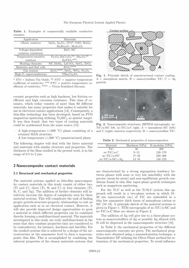
Table 1. Examples of commercially available conductiveceramics.
Application MaterialsOhmic resistors SnO2, In2O3, ITO*, PdO, RuO2,
Bi2Ru2O7, Bi2Ir2O7
Voltage-dependent ZnO, SiCresistors (varistors)
Temperature-sensitive Fe3O4-ZnCr2O4**, Mn3O4**resistors BaTiO3***,
Heating elements SiC,MoSi2 , LaCrO3, SnO2, ZrO2
Batteries and fuel cells ZrO2****Gas sensors ZrO2****, SnO2, WO3, Fe2O3
High-Tc superconductors YBa2Cu3O7
* ITO = Indium Tin Oxide; ** NTC = negative temperaturecoefficient of resistivity; *** PTC = positive temperature co-efficient of resistivity; **** = Yttria Stabilized Zirconia.
ceramic properties such as high hardness, low friction co-efficient and high corrosion resistance. This class of ce-ramics, which today consists of more than 60 differentmaterials, has many properties that makes it suitable foruse in electrical contact applications [14]. Consequently, athin-film technology has been developed, based on PVDmagnetron sputtering utilizing Ti3SiC2 as sputter target.It was then found, that two types of coating materialscould be synthesized from the same source [15]:
– A high-temperature (>800 ◦C) phase consisting of aretained MAX structure.
– A low-temperature (<300 ◦C) nanostructured phase.
The following chapter will deal with the latter materialand materials with similar structure and properties. Thethickness of the films studied in the present work, is in therange of 0.5 to 2 µm.
2 Nanocomposite contact materials
2.1 Structural and mechanical properties
The material systems applied as thin-film nanocompos-ite contact materials in this study consist of either two,(Ti and C), three (Ti, Si and C) or four elements (Ti,Si, C, and Ag). The addition of further elements will in-tuitively increase the degree of complexity seen for thesematerial systems. This will complicate the task of findingproper growth-structure-property relationships to suit anapplication such as in an electrical contact. However, itwill also provide improved design opportunities to growa material in which different properties can be combinedthereby forming a multifunctional material. The materialsinvestigated in this study are truly multifunctional in thesense that they combine properties that are considered tobe contradictory, for instance, hardness and ductility. Forthe studied systems this is achieved by a design of the mi-crostructure at the nanometer level to form a nanocom-posite thin film. This is accomplished by combining theinherent properties of the chosen materials systems that
A
CB
Contact surface
Fig. 1. Principle sketch of nanostructured contact coating.A = amorphous matrix, B = nanocrystalline TiC, C = Agparticle.
Fig. 2. Nanocomposite structures, HRTEM micrographs. nc-TiC/a-SiC left, nc-TiC/a-C right. A = amorphous SiC (left)and C (right) matrices respectively; B = nanocrystalline TiC.
Table 2. Mechanical properties of nanocomposites.
Material Hardness [GPa] E-modulus [GPa]TiC 30 390
nc-TiC/a-C 9–12 120–170nc-TiC/a-SiC 17–23 220–260
nc-TiC/a-SiC+Ag 13–16 140–210
are characterized by a strong segregation tendency be-tween phases with none or very low miscibility with theprecise (atom-by-atom) and non-equilibrium growth con-ditions found in thin film vapor-phase growth techniquessuch as magnetron sputtering.
For the Ti-C as well as the Ti-Si-C system this ap-proach will result in a two-phase system in which 10–20 nm nanocrystals (nc) of TiC are embedded in athin few nanometer thick tissue of amorphous carbon orSiC [16–18]. A principle sketch of the material systems isgiven in Figure 1. TEM micrographs of nc-TiC/a-SiC andnc-TiC/a-C films are shown in Figure 2.
The addition of Ag will give rise to a three-phase sys-tem as nanocrystallites of Ag or possible Ag alloyed withSi will be dispersed in the nanocomposite structure [18].
In Table 2, the mechanical properties of the differentnanocomposite concepts are given. The mechanical prop-erties were obtained using a nanoindentation technique, aNanoindenter XP utilizing the Oliver Pharr method for es-timation of the mechanical properties. To avoid influence
22902-p2
A. Oberg et al.: Nanocomposites for electrical contacts
from the substrate, the indent depths did not exceed 10%of the coating thickness.
The properties of the phases as well as the interfacespresent between them will be highly decisive for the over-all properties of the material. For instance, with respectto mechanical properties the Ti-Si-C system is character-ized by a high hardness and a reduced elastic modulus,yet the material shows pronounced ductility upon inden-tation [17]. The same applies for Ti-C with even morepronounced effects. The first attribute stem from the pres-ence of TiC in the structure whereas the ductility is sug-gested to originate from TiC grain rotation in the softeramorphous SiC or C matrices. The seemingly opposingmechanical properties are not the only noteworthy char-acteristics of these thin-film materials as it also combinesother properties that show similar opposing trends suchas the electrical properties.
2.2 Oxidation and corrosion properties
The stability of the nanocomposites towards oxidation hasnot yet been systematically studied. However, preliminaryresults suggest that both the nc-TiC/a-SiC and nc-TiC/a-C films form rather thin surface oxides in ambient atmo-sphere, X-ray photoelectron (XPS) spectra typically showsmall amounts of Ti-O and Si-O (when Si is present inthe films) suggesting that a mixture of these oxides areformed. The peaks are removed after a few seconds ofsputtering. It should be noted, however, that the surfaceoxidation is related to the grain size of TiC. For exam-ple, in nc-TiC/a-C nanocomposites, the grain size of TiCcan be reduced by increasing the relative amount of car-bon during film growth. XPS analysis of these carbon-richfilms shows more surface oxides which can be attributed tothe fact that a smaller grain size will lead to a larger sur-face area exposed to air and therefore a higher oxidationrate.
The nanocomposite films also seem to exhibit excel-lent corrosion properties. For example, tests of nc-TiC/a-SiC coatings in a Batelle chamber showed excellent resultswith only small amounts of N and Cl in the surface after21 days testing [17]. No S was observed in these films.In contact resistance measurements (coating on crossedrod, ∅10 mm), no significant change was observed. Theaddition of Ag in the surface will, of course, change thechemical stability since Ag is well known to interact withsulphur-containing compounds. The corrosion behavior ofthese materials is currently investigated in more detail andfurther results will be presented elsewhere.
2.3 Resistivity and contact resistance
Resistivity and contact resistance were measured by thefour-terminal method, with an applied current of 5 A whilerecording the voltage drop over the contact. For low con-tact resistance values, measurements were performed withswitched polarity and the mean value of the two measure-ments was given.
Table 3. Resistivity of nanocomposites. Four-terminal mea-surements.
Material Resistivity [µΩcm]TiC 60–80
nc-TiC/a-C 1200–1600nc-TiC/a-SiC 250–350
nc-TiC/a-SiC + Ag 40
���
���
���
��
��
��
��
�
����������������
�������������
���� ����� ���
����� �� ��
����� � ��� �� ��
����������� �� ��
�� �� �� ��������
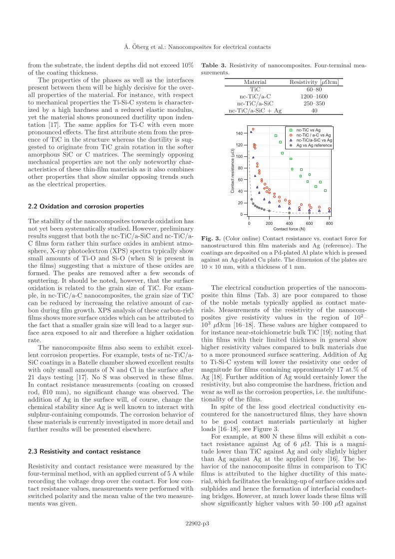
Fig. 3. (Color online) Contact resistance vs. contact force fornanostructured thin film materials and Ag (reference). Thecoatings are deposited on a Pd-plated Al plate which is pressedagainst an Ag-plated Cu plate. The dimension of the plates are10 × 10 mm, with a thickness of 1 mm.
The electrical conduction properties of the nanocom-posite thin films (Tab. 3) are poor compared to thoseof the noble metals typically applied as contact mate-rials. Measurements of the resistivity of the nanocom-posites give resistivity values in the region of 102–103 µΩcm [16–18]. These values are higher compared tofor instance near-stoichiometric bulk TiC [19]; noting thatthin films with their limited thickness in general showhigher resistivity values compared to bulk materials dueto a more pronounced surface scattering. Addition of Agto Ti-Si-C system will lower the resistivity one order ofmagnitude for films containing approximately 17 at.% ofAg [18]. Further addition of Ag would certainly lower theresistivity, but also compromise the hardness, friction andwear as well as the corrosion properties, i.e. the multifunc-tionality of the films.
In spite of the less good electrical conductivity en-countered for the nanostructured films, they have shownto be good contact materials particularly at higherloads [16–18], see Figure 3.
For example, at 800 N these films will exhibit a con-tact resistance against Ag of 6 µΩ. This is a magni-tude lower than TiC against Ag and only slightly higherthan Ag against Ag at the applied force [16]. The be-havior of the nanocomposite films in comparison to TiCfilms is attributed to the higher ductility of this mate-rial, which facilitates the breaking-up of surface oxides andsulphides and hence the formation of interfacial conduct-ing bridges. However, at much lower loads these films willshow significantly higher values with 50–100 µΩ against
22902-p3
The European Physical Journal Applied Physics
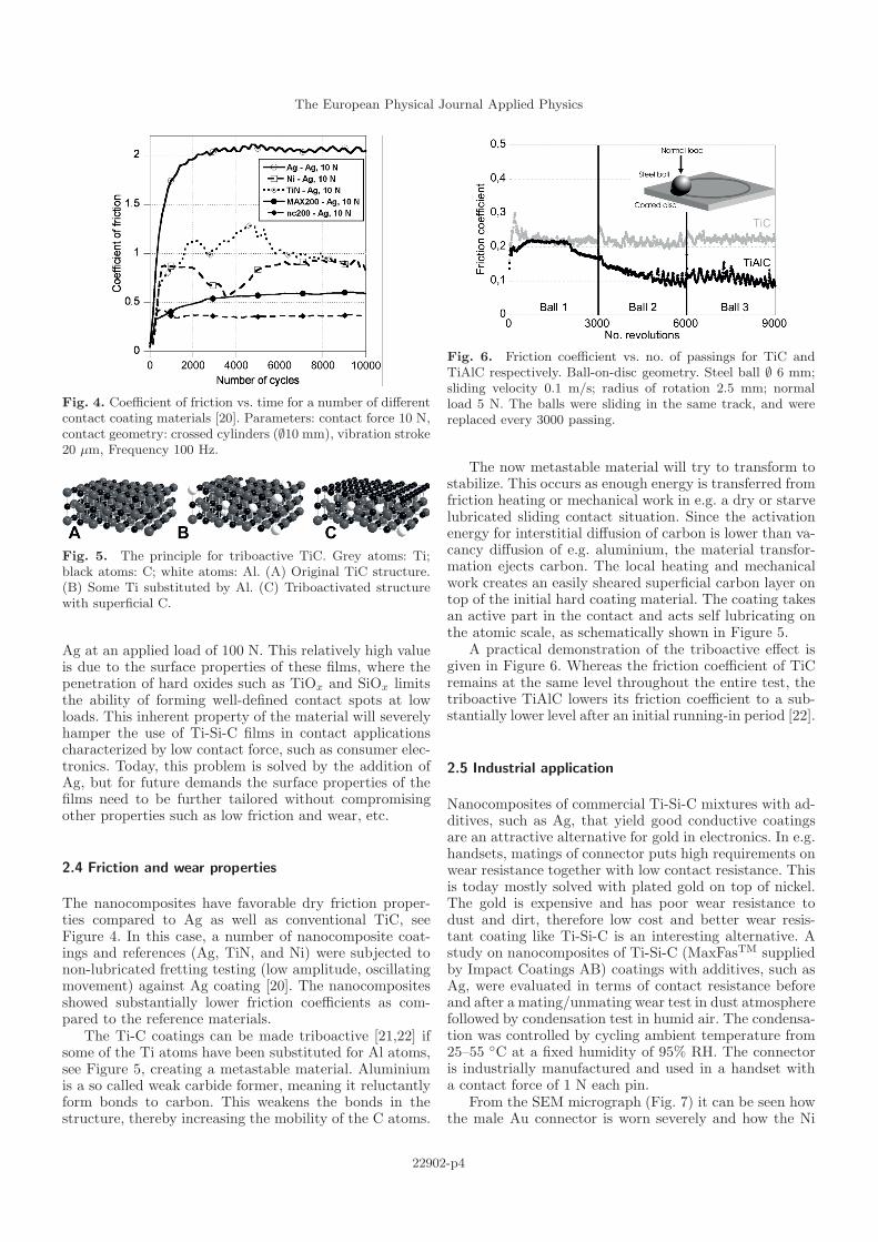
Fig. 4. Coefficient of friction vs. time for a number of differentcontact coating materials [20]. Parameters: contact force 10 N,contact geometry: crossed cylinders (∅10 mm), vibration stroke20 µm, Frequency 100 Hz.
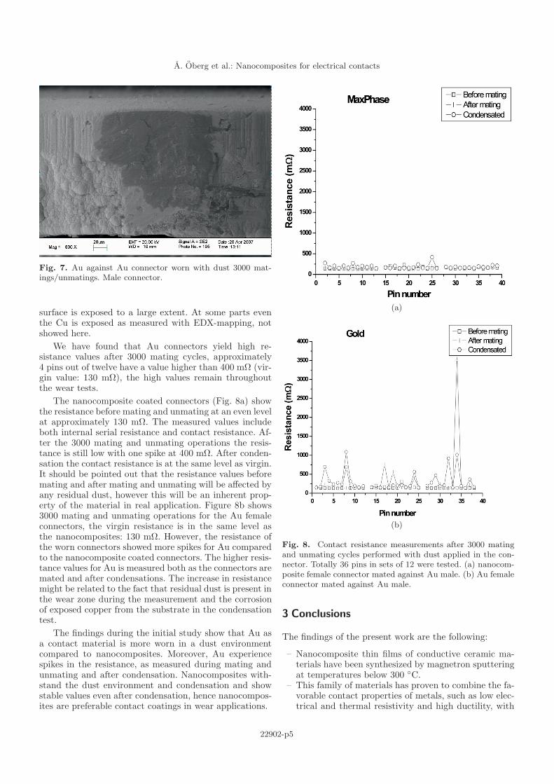
Fig. 5. The principle for triboactive TiC. Grey atoms: Ti;black atoms: C; white atoms: Al. (A) Original TiC structure.(B) Some Ti substituted by Al. (C) Triboactivated structurewith superficial C.
Ag at an applied load of 100 N. This relatively high valueis due to the surface properties of these films, where thepenetration of hard oxides such as TiOx and SiOx limitsthe ability of forming well-defined contact spots at lowloads. This inherent property of the material will severelyhamper the use of Ti-Si-C films in contact applicationscharacterized by low contact force, such as consumer elec-tronics. Today, this problem is solved by the addition ofAg, but for future demands the surface properties of thefilms need to be further tailored without compromisingother properties such as low friction and wear, etc.
2.4 Friction and wear properties
The nanocomposites have favorable dry friction proper-ties compared to Ag as well as conventional TiC, seeFigure 4. In this case, a number of nanocomposite coat-ings and references (Ag, TiN, and Ni) were subjected tonon-lubricated fretting testing (low amplitude, oscillatingmovement) against Ag coating [20]. The nanocompositesshowed substantially lower friction coefficients as com-pared to the reference materials.
The Ti-C coatings can be made triboactive [21,22] ifsome of the Ti atoms have been substituted for Al atoms,see Figure 5, creating a metastable material. Aluminiumis a so called weak carbide former, meaning it reluctantlyform bonds to carbon. This weakens the bonds in thestructure, thereby increasing the mobility of the C atoms.
Fig. 6. Friction coefficient vs. no. of passings for TiC andTiAlC respectively. Ball-on-disc geometry. Steel ball ∅ 6 mm;sliding velocity 0.1 m/s; radius of rotation 2.5 mm; normalload 5 N. The balls were sliding in the same track, and werereplaced every 3000 passing.
The now metastable material will try to transform tostabilize. This occurs as enough energy is transferred fromfriction heating or mechanical work in e.g. a dry or starvelubricated sliding contact situation. Since the activationenergy for interstitial diffusion of carbon is lower than va-cancy diffusion of e.g. aluminium, the material transfor-mation ejects carbon. The local heating and mechanicalwork creates an easily sheared superficial carbon layer ontop of the initial hard coating material. The coating takesan active part in the contact and acts self lubricating onthe atomic scale, as schematically shown in Figure 5.
A practical demonstration of the triboactive effect isgiven in Figure 6. Whereas the friction coefficient of TiCremains at the same level throughout the entire test, thetriboactive TiAlC lowers its friction coefficient to a sub-stantially lower level after an initial running-in period [22].
2.5 Industrial application
Nanocomposites of commercial Ti-Si-C mixtures with ad-ditives, such as Ag, that yield good conductive coatingsare an attractive alternative for gold in electronics. In e.g.handsets, matings of connector puts high requirements onwear resistance together with low contact resistance. Thisis today mostly solved with plated gold on top of nickel.The gold is expensive and has poor wear resistance todust and dirt, therefore low cost and better wear resis-tant coating like Ti-Si-C is an interesting alternative. Astudy on nanocomposites of Ti-Si-C (MaxFasTM suppliedby Impact Coatings AB) coatings with additives, such asAg, were evaluated in terms of contact resistance beforeand after a mating/unmating wear test in dust atmospherefollowed by condensation test in humid air. The condensa-tion was controlled by cycling ambient temperature from25–55 ◦C at a fixed humidity of 95% RH. The connectoris industrially manufactured and used in a handset witha contact force of 1 N each pin.
From the SEM micrograph (Fig. 7) it can be seen howthe male Au connector is worn severely and how the Ni
22902-p4
A. Oberg et al.: Nanocomposites for electrical contacts
Fig. 7. Au against Au connector worn with dust 3000 mat-ings/unmatings. Male connector.
surface is exposed to a large extent. At some parts eventhe Cu is exposed as measured with EDX-mapping, notshowed here.
We have found that Au connectors yield high re-sistance values after 3000 mating cycles, approximately4 pins out of twelve have a value higher than 400 mΩ (vir-gin value: 130 mΩ), the high values remain throughoutthe wear tests.
The nanocomposite coated connectors (Fig. 8a) showthe resistance before mating and unmating at an even levelat approximately 130 mΩ. The measured values includeboth internal serial resistance and contact resistance. Af-ter the 3000 mating and unmating operations the resis-tance is still low with one spike at 400 mΩ. After conden-sation the contact resistance is at the same level as virgin.It should be pointed out that the resistance values beforemating and after mating and unmating will be affected byany residual dust, however this will be an inherent prop-erty of the material in real application. Figure 8b shows3000 mating and unmating operations for the Au femaleconnectors, the virgin resistance is in the same level asthe nanocomposites: 130 mΩ. However, the resistance ofthe worn connectors showed more spikes for Au comparedto the nanocomposite coated connectors. The higher resis-tance values for Au is measured both as the connectors aremated and after condensations. The increase in resistancemight be related to the fact that residual dust is present inthe wear zone during the measurement and the corrosionof exposed copper from the substrate in the condensationtest.
The findings during the initial study show that Au asa contact material is more worn in a dust environmentcompared to nanocomposites. Moreover, Au experiencespikes in the resistance, as measured during mating andunmating and after condensation. Nanocomposites with-stand the dust environment and condensation and showstable values even after condensation, hence nanocompos-ites are preferable contact coatings in wear applications.
(a)
(b)
Fig. 8. Contact resistance measurements after 3000 matingand unmating cycles performed with dust applied in the con-nector. Totally 36 pins in sets of 12 were tested. (a) nanocom-posite female connector mated against Au male. (b) Au femaleconnector mated against Au male.
3 Conclusions
The findings of the present work are the following:
– Nanocomposite thin films of conductive ceramic ma-terials have been synthesized by magnetron sputteringat temperatures below 300 ◦C.
– This family of materials has proven to combine the fa-vorable contact properties of metals, such as low elec-trical and thermal resistivity and high ductility, with
22902-p5
The European Physical Journal Applied Physics
those of ceramics such as low friction and wear rateand high chemical integrity.
– The tribological properties of this type of materialscan be tailored by alloying with a weak carbide former(Al) which creates a triboactive system.
– A substantial improvement in performance of a real-life contact system can be achieved by utilizing ananocomposite coating.
The basic research on nanocomposites is very dynamic andit is expected that new material and system concepts willfurther improve functionality and performance of electri-cal contact systems.
The authors wish to acknowledge the financial support of theSwedish Foundation for Strategic Research (SSF), Swedish Re-search Council (VR) and the Swedish Agency for InnovationSystems (VINNOVA). We also wish to thank P.O. A. Perssonof IFM, Linkoping University, for providing excellent HRTEMmicrographs.
References
1. R. Holm, Electric Contacts, 4th edn. (Springer-Verlag,Berlin, 2000)
2. M. Antler, S.J. Krumbein, in Proc. 11th EngineeringSeminar on Electrical Contacts, Orono, USA, 1965, p. 103
3. J.C. Kosco, in Proc. 14th Holm Seminar on ElectricContact Phenomena, Chicago, USA, 1968, p. 55
4. P.G. Slade, C.Y. Lin, A.R. Pebler, in Proc. 26th HolmConf. on Electrical Contacts, Chicago, USA, 1980, p. 271
5. Electrical Contacts, 1st edn., edited by P.G. Slade (MarcelDekker, New York, 1999), Chaps. 1, 13, 15 and 16
6. C. Ernsberger, J. Nickerson, A.E. Miller, J.F. Moulder, inProc. 30th Holm Conf. on Electrical Contacts, Chicago,USA, 1984, p. 587
7. S. Benhenda, J.M. Guglielmacci, M. Gillet, L. Hultman,J.-E. Sundgren, Appl. Surf. Sci. 40, 121 (1989)
8. S. Benhenda, N. Ben Jemaa, D. Travers, C. Perrin,D. Simon, in Proc. Int. Conf. on Electric Contacts,Loughborough, 1992, p. 181
9. A. Kassman-Rudolphi, S. Jacobson, Surf. Coat. Technol.89, 270 (1997)
10. C. Kittel, Introduction to Solid State Physics, 8th edn.(John Wiley & Sons, New York, 2004)
11. A.J. Moulson, J.M. Herbert, Electroceramics, 2nd edn.(John Wiley & Sons, New York, 2003)
12. M.W. Barsoum, T. El-Raghy, J. Am. Ceram. Soc. 79, 1953(1996)
13. M.W. Barsoum, T. El-Raghy, Am. Scientist 89, 334 (2001)14. P. Isberg, T. Liljenberg, L. Hultman, U. Jansson, ABB
Review 1, 64 (2004)15. J. Emmerlich et al., J. Appl. Phys. 96, 4817 (2004)16. E. Lewin, O. Wilhelmsson, U. Jansson, J. Appl. Phys. 100,
054303 (2006)17. P. Eklund, J. Emmerlich, H. Hogberg, O. Wilhelmsson, P.
Isberg, J. Birch, P.O. A. Persson, U. Jansson, L. Hultman,J. Vac. Sci. Technol. B 23, 2486 (2005)
18. P. Eklund, T. Joelsson, H. Ljungcrantz, O. Wilhelmsson,Zs. Czigany, H. Hogberg, L. Hultman, Surf. Coat.Technnol. 201, 6465 (2007)
19. W.S. Williams, Mat. Sci. Eng. A 105-106, 1 (1988)20. B. Andre, A. Kassman-Rudolphi, in Proc. Eur. Conf. on
Tribology (ECOTRIB), Ljubljana, Slovenia, 2007, p. 8121. O. Wilhelmsson et al., Adv. Funct. Mater. 17, 1611 (2007)22. M. Lindquist, O. Wilhelmsson, U. Jansson, U. Wiklund,
Wear 266, 379 (2009)
22902-p6


![Nanocomposite polymer electrolyte for rechargeable magnesium batteries · batteries in which a stable, but Li + conductive SEI is formed [32]. To date, functional electrolytes for](https://static.fdocuments.us/doc/165x107/5fd5d4a5ea33333dc711f93c/nanocomposite-polymer-electrolyte-for-rechargeable-magnesium-batteries-batteries.jpg)