Conductance Maps by Electrochemical Tunneling Spectroscopy To Fingerprint the Electrode Electronic...
5
Technical Notes Conductance Maps by Electrochemical Tunneling Spectroscopy To Fingerprint the Electrode Electronic Structure IsmaelDı´ez-Pe ´ rez, Aleix G. Gu 1 ell, Fausto Sanz,* , and Pau Gorostiza* ,‡ Laboratory of Electrochemistry and Materials (LCTEM), Department of Physical Chemistry, University of Barcelona, Martı ´ i Franque ` s 1, 08028 Barcelona, Spain, and Centre de Refere ` ncia en Bioenginyeria de Catalunya, Parc Cientific de Barcelona, Josep Samitier 1, Barcelona 08028, Spain We describe a methodology to perform reliable tunneling spectroscopy in electrochemical media. Sequential in situ tunneling spectra are recorded while the electrochemical potential of the electrode is scanned. Spectroscopic data are presented as conductance maps or conductograms that show the in situ electronic structure of an electrode surface while it undergoes an electrochemical reaction. The conductance map or conductogram represents the redox fingerprint of an electrode/liquid interface in a specific medium and can serve to predict its electrochemi- cal behavior in a quantitative energy scale. The methodol- ogy is validated studying the reversible oxidation and passivity of an iron electrode in borate buffer, and we describe the main quantitative information that can be extracted concerning the semiconducting properties of the Fe passive film. This methodology is useful to study heterogeneous catalysis, electrochemical sensing and bioelectronic systems. The use of (electro)chemical-based techniques has become an essential part of the study of fundamental processes in fields such as sensing, 1 catalysis, 2 passivation/corrosion, 3,4 crystal growth, 5 or electron transport through (bio)organic molecules. 6 Although in situ measurements are essential to study directly the chemical-physical properties of electrode/liquid interfaces and the processes occurring therein, they are technically challenging and few techniques are available. Since the first applications of scanning tunneling microscopy (STM) to solid/liquid interfaces, 7 a variety of studies can be found showing spatial resolution up to the atomic scale. 8,9 STM also allows the implementation of an electrochemical cell through a four-electrode configuration (EC- STM), which enables control of the redox processes occurring at the electrode surface. 8 Electrochemical scanning tunneling spec- troscopy (ECTS) provides a unique opportunity to probe in situ the local electronic properties of the electrode/liquid interface. Tao was the first to obtain spectroscopic information of a redox biomolecular system by using ECSTM imaging at different substrate potentials. 10a In parallel, several papers demonstrated the practical realization of ECTS. 10b-14 However, several technical difficulties have hindered its wide application. To use ECTS as a robust electrochemical tool, it is essential to have the following: (i) accurate independent control of both tip and sample potential that ensures the chemical stability of the surfaces electrode, (ii) real reference electrodes that maintain the electrochemical potentials throughout the experiment, and (iii) suitable STM probes that provide a wide potential range and a low leak current during the fast tip voltage ramps used to minimize thermal drift. We have recently developed an electrochemical STM setup and tip preparation method to strictly satisfy all of these requirements. An interesting system to assess with ECTS is iron electrode passivation, which is an extensively studied process 15-17 owing to its wide technological application and the economical impact that corrosion has on Fe and Fe-based alloys. Although the detailed * Corresponding authors. E-mail: [email protected]. phone: +34 4021240. Fax: +34 4021231. E-mail: [email protected]. phone: +34 4037185. Fax: +34 4037181. University of Barcelona. ‡ Parc Cientific de Barcelona. (1) Park, N.; Hahn, J. H. Anal. Chem. 2005, 77, 7100-7100. (2) Maroun, F.; Ozanam, F.; Magnussen, M.; Behm, R. J. Science 2001, 293, 1811-1814. (3) Ryan, M. P.; Williams, D. E.; Chater, R. J.; B. M. Hutton, McPhail, D. S. Nature 2002, 415, 770-774. (4) Punckt, C.; Bo ¨lscher, M.; Rotermund, H. H.; Mikhailov, A. S.; Organ, L.; Budiansky, N.; Scully, J. R.; Hudson, J. L. Science 2004, 305, 1133-1136. (5) Macpherson, J. V.; Unwin, P. R.; Hillier, A. C.; Bard, A. J. J. Am. Chem. Soc. 1996, 118, 6445-6452. (6) Xu, B. Q.; Li, X. L.; Xiao, X. Y.; Sakaguchi, H.; Tao, N. J. Nano Lett. 2005, 5, 1491-1495. (7) Sonnenfeld, R.; Hansma, P. K.; Science 1986, 232, 211-213. (8) (a) Liu, H.-Y.; Fan, F. R. F.; Lin, C. W.; Bard, A. J. J. Am. Chem. Soc. 1986, 108, 3838-3839. (b) Gao, X.; Weaver, M. J. Phys. Rev. Lett. 1994, 73, 846- 849. (c) Dietterle, M.; Will, T.; Kolb, D. M. Surf. Sci. 1998, 396, 189-197. (9) Yao, H.; Yau, S.-L.; Itaya, K. Appl. Phys. Lett. 1996, 68, 1473-1475. (10) (a) Tao, N. J. Phys. Rev. Lett. 1996, 73, 846-849. (b) Hugelmann, P.; Schindler, W. J. Phys. Chem. B 2005, 109, 6262-6267. (11) Tomita, E.; Matsuda, N.; Itaya, K. J. Vac. Technol., A 1990, 8, 534-538. (12) Azumi, K.; Araki, K.; Seo, M. J. Electroanal. Chem. 1997, 427, 15-21. (13) Abadal, G.; Pe ´ rez-Murano, F.; Barniol, N.; Borrise ´, X.; Aymerich, X. Ultramicroscopy 1996, 66, 133-139. (14) Halbritter, J.; Repphun, G.; Vinzelberg, S.; Staikov, G.; Lorenz, W. J. Electrochim. Acta 1995, 40, 1385-1394. (15) Bu ¨chler, M.; Schmuki, P.; Bo ¨hni, H. J. Electrochem. Soc. 1998, 145, 609- 614. (16) Buchler, M.; Schmuki, P.; Bohni, H.; Stenberg, T.; Ma ¨ntyla ¨, T. J. Electrochem. Soc. 1998, 145, 378-385. Anal. Chem. 2006, 78, 7325-7329 10.1021/ac0603330 CCC: $33.50 © 2006 American Chemical Society Analytical Chemistry, Vol. 78, No. 20, October 15, 2006 7325 Published on Web 09/20/2006
Transcript of Conductance Maps by Electrochemical Tunneling Spectroscopy To Fingerprint the Electrode Electronic...
Technical Notes
Conductance Maps by Electrochemical TunnelingSpectroscopy To Fingerprint the ElectrodeElectronic Structure
Ismael Dıez-Perez,† Aleix G. Gu1ell,† Fausto Sanz,*,† and Pau Gorostiza*,‡
Laboratory of Electrochemistry and Materials (LCTEM), Department of Physical Chemistry, University of Barcelona,Martı i Franques 1, 08028 Barcelona, Spain, and Centre de Referencia en Bioenginyeria de Catalunya, Parc Cientific deBarcelona, Josep Samitier 1, Barcelona 08028, Spain
We describe a methodology to perform reliable tunnelingspectroscopy in electrochemical media. Sequential in situtunneling spectra are recorded while the electrochemicalpotential of the electrode is scanned. Spectroscopic dataare presented as conductance maps or conductogramsthat show the in situ electronic structure of an electrodesurface while it undergoes an electrochemical reaction.The conductance map or conductogram represents theredox fingerprint of an electrode/liquid interface in aspecific medium and can serve to predict its electrochemi-cal behavior in a quantitative energy scale. The methodol-ogy is validated studying the reversible oxidation andpassivity of an iron electrode in borate buffer, and wedescribe the main quantitative information that can beextracted concerning the semiconducting properties of theFe passive film. This methodology is useful to studyheterogeneous catalysis, electrochemical sensing andbioelectronic systems.
The use of (electro)chemical-based techniques has becomean essential part of the study of fundamental processes in fieldssuch as sensing,1 catalysis,2 passivation/corrosion,3,4 crystalgrowth,5 or electron transport through (bio)organic molecules.6
Although in situ measurements are essential to study directly thechemical-physical properties of electrode/liquid interfaces andthe processes occurring therein, they are technically challengingand few techniques are available. Since the first applications of
scanning tunneling microscopy (STM) to solid/liquid interfaces,7
a variety of studies can be found showing spatial resolution up tothe atomic scale.8,9 STM also allows the implementation of anelectrochemical cell through a four-electrode configuration (EC-STM), which enables control of the redox processes occurring atthe electrode surface.8 Electrochemical scanning tunneling spec-troscopy (ECTS) provides a unique opportunity to probe in situthe local electronic properties of the electrode/liquid interface.Tao was the first to obtain spectroscopic information of a redoxbiomolecular system by using ECSTM imaging at differentsubstrate potentials. 10a In parallel, several papers demonstratedthe practical realization of ECTS.10b-14 However, several technicaldifficulties have hindered its wide application. To use ECTS as arobust electrochemical tool, it is essential to have the following:(i) accurate independent control of both tip and sample potentialthat ensures the chemical stability of the surfaces electrode, (ii)real reference electrodes that maintain the electrochemicalpotentials throughout the experiment, and (iii) suitable STMprobes that provide a wide potential range and a low leak currentduring the fast tip voltage ramps used to minimize thermal drift.We have recently developed an electrochemical STM setup andtip preparation method to strictly satisfy all of these requirements.
An interesting system to assess with ECTS is iron electrodepassivation, which is an extensively studied process15-17 owing toits wide technological application and the economical impact thatcorrosion has on Fe and Fe-based alloys. Although the detailed
* Corresponding authors. E-mail: [email protected]. phone: +34 4021240. Fax:+34 4021231. E-mail: [email protected]. phone: +34 4037185. Fax: +344037181.
† University of Barcelona.‡ Parc Cientific de Barcelona.
(1) Park, N.; Hahn, J. H. Anal. Chem. 2005, 77, 7100-7100.(2) Maroun, F.; Ozanam, F.; Magnussen, M.; Behm, R. J. Science 2001, 293,
1811-1814.(3) Ryan, M. P.; Williams, D. E.; Chater, R. J.; B. M. Hutton, McPhail, D. S.
Nature 2002, 415, 770-774.(4) Punckt, C.; Bolscher, M.; Rotermund, H. H.; Mikhailov, A. S.; Organ, L.;
Budiansky, N.; Scully, J. R.; Hudson, J. L. Science 2004, 305, 1133-1136.(5) Macpherson, J. V.; Unwin, P. R.; Hillier, A. C.; Bard, A. J. J. Am. Chem.
Soc. 1996, 118, 6445-6452.(6) Xu, B. Q.; Li, X. L.; Xiao, X. Y.; Sakaguchi, H.; Tao, N. J. Nano Lett. 2005,
5, 1491-1495.
(7) Sonnenfeld, R.; Hansma, P. K.; Science 1986, 232, 211-213.(8) (a) Liu, H.-Y.; Fan, F. R. F.; Lin, C. W.; Bard, A. J. J. Am. Chem. Soc. 1986,
108, 3838-3839. (b) Gao, X.; Weaver, M. J. Phys. Rev. Lett. 1994, 73, 846-849. (c) Dietterle, M.; Will, T.; Kolb, D. M. Surf. Sci. 1998, 396, 189-197.
(9) Yao, H.; Yau, S.-L.; Itaya, K. Appl. Phys. Lett. 1996, 68, 1473-1475.(10) (a) Tao, N. J. Phys. Rev. Lett. 1996, 73, 846-849. (b) Hugelmann, P.;
Schindler, W. J. Phys. Chem. B 2005, 109, 6262-6267.(11) Tomita, E.; Matsuda, N.; Itaya, K. J. Vac. Technol., A 1990, 8, 534-538.(12) Azumi, K.; Araki, K.; Seo, M. J. Electroanal. Chem. 1997, 427, 15-21.(13) Abadal, G.; Perez-Murano, F.; Barniol, N.; Borrise, X.; Aymerich, X.
Ultramicroscopy 1996, 66, 133-139.(14) Halbritter, J.; Repphun, G.; Vinzelberg, S.; Staikov, G.; Lorenz, W. J.
Electrochim. Acta 1995, 40, 1385-1394.(15) Buchler, M.; Schmuki, P.; Bohni, H. J. Electrochem. Soc. 1998, 145, 609-
614.(16) Buchler, M.; Schmuki, P.; Bohni, H.; Stenberg, T.; Mantyla, T. J. Electrochem.
Soc. 1998, 145, 378-385.
Anal. Chem. 2006, 78, 7325-7329
10.1021/ac0603330 CCC: $33.50 © 2006 American Chemical Society Analytical Chemistry, Vol. 78, No. 20, October 15, 2006 7325Published on Web 09/20/2006

mechanism is still a subject of debate, the phenomenon of passivityis based on the spontaneous formation of an oxide film, a fewnanometers thick, that effectively protects metal from corrosion.18
Passive films can be created in an electrochemical cell by thecontrolled application of oxidizing electrochemical potentials inneutral and alkaline media. In the case of iron, the electronicproperties of the surface can be driven from metallic (negativepotential) to semiconducting Fe(III) oxide (positive potential),which offers a great variation to be tested by ECTS. The resultingsemiconducting passive film has a large band gap, n-type proper-ties, and a high doping density.15-17,19 The electrochemicalimplications of these electronic properties are not completelyunderstood, and speculative models have been proposed.20,21
In this contribution, we present a novel in situ analytical toolfor the characterization of electrode/liquid interfaces based onECTS technique. Our method allows us to measure conductancespectra of an electrode in the absolute energy scale and as afunction of its oxidation state. These spectra can be directlycompared to spectra acquired in air and vacuum, but are notaffected by artifacts like the tip-induced band bending (seeSupporting Information). Spectroscopic data are presented as 3-Dconductance maps that outline the electronic structure of theelectrode surface in the solution of interest. We have validatedthis methodology with an iron electrode that is reversibly oxidizedin borate buffer solution throughout the entire electrochemicalrange.17 The resulting conductance map of iron in borate,measured directly and locally at the nanoscale, is then useful tounderstand the macroscopic electrochemical behavior of iron.
EXPERIMENTAL SECTIONChemicals. The recording liquid electrolyte (borate buffer
solutions) was made of 0.3 M H3BO3 and 0.0375 M Na2B4O7‚10H2O and gives a pH value of 7.5. Solutions were prepared withpro analysi purity grade chemicals from Merck (Darmstadt,Germany) and Milli-Q water of 18 MΩ‚cm. All experiments wereperformed under an oxygen free atmosphere. This stage is veryimportant since electroactive oxygen can be one of the mainsources of the electrochemical current noise at the STM tip.10 Forthat reason, in addition to 20-min nitrogen bubbling of all boratebuffer solutions, the experiments were conducted in a sealedchamber under nitrogen atmosphere which was part of our STMsystem.
Substrate Preparation. The samples used in this study weremechanically polished polycrystalline iron disks 99.99%, 0.3 mmthick and 10 mm in diameter. The chemical purity of this surfacewas previously checked ex situ by X-ray photoelectron spectros-copy.17 The polishing procedure involved a first step of grindingby silicon carbide polishing papers of 30-, 9-, 5-, 3-, and 1-µmparticle size, successively, and then finishing with 0.3-µm alumi-num oxide powder. Between each polishing step, the iron surfaceswere sonicated in Milli-Q water and ethanol. Before each experi-ment, the samples were thoroughly rinsed in different solvents
in order to remove organic contamination from the surface,followed by a final rinse in Milli-Q water. With this treatment, weobtained a mirrorlike surface with a mean roughness of typicallyless than 2 nm.
ECTS and Electrochemical Measurements. We used anelectrochemical STM setup composed of a pico-SPM microscope(Molecular Imaging, Phoenix, AZ) controlled through a Nano-scope IIIa electronics (Veeco Instruments, Santa Barbara, CA),which was plugged to a signal access module that allows externalapplication of fast voltage ramps using a signal generator (AgilentTechnologies) and fast output data capturing in real time using adigital oscilloscope (Tektronix). This configuration allows stableand independent electrochemical potential control of both sampleand tip (US and UT, respectively), which were placed in a smallelectrochemical cell connected to a bipotentiostat (Picostat,Molecular Imaging), and a real miniaturized home-built Ag/AgClreference electrode (SSC). A circular Pt wire served as a counterelectrode. It is advantageous to quote directly UT and US in theelectrochemical scale (mV/SSC) instead of the sample bias (US
- UT), so that the Fermi level of tip and sample can be directlyplaced in energy diagrams. A scheme of our experimental setupis provided in Figure 1. Typically, our tunneling current versusUT ramps spanned up to 2.5 V, covering the entire energy rangeof interest. Scan rates were up to 20 V/s and lasted less than 100ms to minimize tip drift. These ramps require extremely wellinsulated STM tips in order to minimize electrochemical currents(faradaic and capacitive currents) exchanged at the tip andgenerated when UT is rapidly ramped in a conductive media. Leakcurrents below 0.5 nA can be routinely obtained with proper tippreparation22 and were further reduced by acquiring blank spectraat 3 nm of the surface at each US value.13 Further technicalinformation and other experimental details can be found in theSupporting Information. Cyclic voltammetry was performed with
(17) (a) Dıez-Perez, I.; Gorostiza, P.; Sanz, F. J. Electrochem. Soc. 2003, 150,B348-B354. (b) Dıez-Perez, I.; Gorostiza, P.; Sanz, F.; Muller, C. J.Electrochem. Soc. 2001, 148, B307-B313.
(18) Schonbein, C. Ann. Phys. Chem. 1836, 37, 390-399.(19) Morrison, S. R., Ed. Electrochemistry at Semiconductor and Oxidized Metal
Electrodes; Plenum Press: New York, 1980.(20) Gerischer, H. Corros. Sci. 1989, 29, 191-195.(21) Sato, N. Corros. Sci. 1990, 31, 1-19.
(22) Guell, A. G.; Dıez-Perez, I.; Gorostiza, P.; Sanz, F. Anal. Chem. 2004, 76,5218-5222.
Figure 1. Simplified experimental setup showing the electrochemi-cal cell with a 4-electrode configuration: metallic working electrode(WE), Pt counter electrode (CE), SSC reference electrode (RE), andSTM tip electrode. This configuration allows independent voltagecontrol of the electrochemical potentials UT and US. STM bias isdefined as US-UT.
7326 Analytical Chemistry, Vol. 78, No. 20, October 15, 2006

Solartron electrochemical interface SI 1287 model using a standardelectrochemical cell under static hydrodynamic conditions.
RESULTS AND DISCUSSIONPrior to the acquisition of current-voltage ECTS spectra, it
was essential to evaluate the local energy barrier height (Φ) atevery surface oxidation state in order to ensure the same initialtunneling conditions and to compensate the tunneling junction(see Supporting Information). Barriers Φ can be accuratelycalculated from the slope of the tip current (IT) versus tip-sampledistance (s), through the relation14 Φ(eV) ) 0.952 (d ln IT/ds)2.The IT versus s plots of metallic and oxidized Fe electrode in boratebuffer (Figure 2a and b, respectively) show a clearly exponentialbehavior. We have found that, using UT e -320 mV, goodtunneling conditions and reproducible barrier measurements areobtained for all US. At these UT values, electrons are injected intothe empty states of the metal or into the conduction band (CB)of the oxide (the CB edge of the Fe passive film is located at-320 ( 20 mV;17 see inset plot of Figure 2). The obtainedtunneling barriers are Φ ) 0.30 ( 0.06 eV at US ) -800 mV(corresponding to metallic Fe(0), Figure 2a) and Φ ) 0.26 ( 0.04eV at US ) +500 mV (corresponding to passive Fe(III) oxide,Figure 2b). The fact that the same tunneling barrier is observedfor the metallic and fully oxidized states indicates that, at theseUT, the rate-limiting step is electron tunneling through the liquidgap (Helmholtz layer19), with minor contributions due to the spacecharge region in the oxide. Using UT near or within the band gapleads to poor tunneling conditions, as indicated by nonexponentialbehavior (Figure 2c) and a large scatter in the barrier measure-ments.23 At these US, the tip is partially crashed on the surface ascan be seen from the long retraction required to detach it (Figure2d). It is thus essential to select UT such that the same initialtunneling conditions are maintained throughout the entire con-ductance map (i.e., in all ECTS spectra at different US (oxidationstate) values).
Once stable tunneling conditions are established, it is possibleto obtain comparable tunneling spectra of the iron electrode
surface as it is reversibly oxidized between US ) -1000 and +1100mV. At every US value, an initial UT e -320 mV is set beforedisconnecting the STM feedback loop. ECTS spectra are thenacquired by scanning UT between -800 and +1500 mV while IT
is recorded. The IT(UT) characteristics are shown in Figure 3a.IT(UT) plots are differentiated to obtain the local conductance dIT/dUT (Figure 3b), which is proportional to the density of states atthe different electron energies.14 Since they are measured versusa reference electrode in solution, tip current and conductance canbe represented in an electron energy scale given in electronvoltsversus the vacuum level24 (top axis, Figure 3a). The sameprocedure is repeated at different US (electrode oxidation state),and series of ECTS are thus recorded.
ECTS spectra change strongly with the potential applied tothe iron electrode US (Figure 3a), and these changes are directlyrelated to the electrochemical state of iron within each potentialrange.17 Between US ) -800 and -650 mV, iron is fully reducedto metallic state (Fe(0)) and displays linear ECTS as correspondsto a high density of surface states or a high surface conductance(Figure 3a and b). At US ) -400 mV, releasing of Fe2+(aq) speciesinto the solution gives rise to a hydrated Fe(II) oxide layer16,17
with unknown electronic properties. Within this range and after
(23) Schreyer, A.; Eng, L.; Bohni, H. J. Vac. Technol. 1996, B14, 1162-1166. (24) Gerischer, H.; Ekardt, W. Appl. Phys. Lett. 1983, 43, 393-395.
Figure 2. Averaged (N g 5) IT(s) plots at different UT and Feoxidation states (US). Exponentially decreasing currents correspondto stable tunneling conditions. Similar barriers are obtained at UT )-770 mV, US ) -800 mV (Fe(0), curve a) and UT ) -770 mV, US
) 500 mV (Fe(III), curve b), which correspond to electron injectioninto the conduction band (see inset). On the iron(III) oxide surface,setting UT within the band gap region gives rise to a nonexponentialcurrent behavior, as shown by example traces at UT ) 100 mV, US
) 500 mV (curve c) and UT ) 300 mV, US ) 500 mV (curve d).
Figure 3. ECTS spectra of Fe in borate buffer at different oxidationstates (US). Solid lines are averaged spectra, and gray bands indicatestandard deviation (N g 10). (a) Spectra are linear for metallic Fe(0)(US ) -800 and -650 mV) and show a double-exponential behavioras iron is oxidized to Fe(II) (US ) -400 mV) and to Fe(III) (US ) 500and 900 mV). The positive branch is maintained by a current ofelectrons under slight electron depletion (US ) 500 mV, upper inset,#) but is extinguished at stronger depletion conditions (US ) 900 mV,lower inset, ##). (b) Tunneling conductance of ECTS spectra iscalculated by differentiation of the curves in (a). Initial setpointconditions were IT ) 5 nA and UT ) -800 mV. Electrochemical STMimages of the Fe(III) surface (US ) 500 mV, 400 × 400 nm2) showsthat imaging is only possible by electron injection into the conductionband (UT e -320 mV).
Analytical Chemistry, Vol. 78, No. 20, October 15, 2006 7327
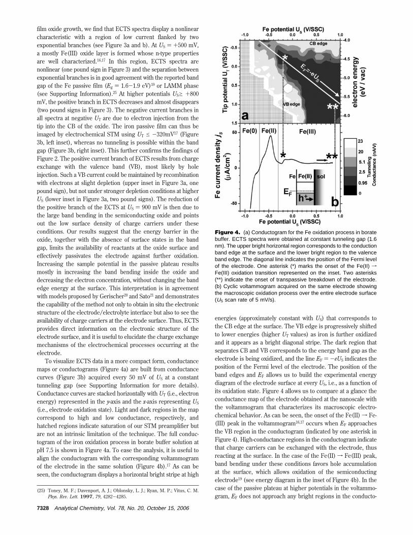
film oxide growth, we find that ECTS spectra display a nonlinearcharacteristic with a region of low current flanked by twoexponential branches (see Figure 3a and b). At US ) +500 mV,a mostly Fe(III) oxide layer is formed whose n-type propertiesare well characterized.16,17 In this region, ECTS spectra arenonlinear (one pound sign in Figure 3) and the separation betweenexponential branches is in good agreement with the reported bandgap of the Fe passive film (Eg ) 1.6-1.9 eV)19 or LAMM phase(see Supporting Information).25 At higher potentials USg +800mV, the positive branch in ECTS decreases and almost disappears(two pound signs in Figure 3). The negative current branches inall spectra at negative UT are due to electron injection from thetip into the CB of the oxide. The iron passive film can thus beimaged by electrochemical STM using UT e -320mV17 (Figure3b, left inset), whereas no tunneling is possible within the bandgap (Figure 3b, right inset). This further confirms the findings ofFigure 2. The positive current branch of ECTS results from chargeexchange with the valence band (VB), most likely by holeinjection. Such a VB current could be maintained by recombinationwith electrons at slight depletion (upper inset in Figure 3a, onepound sign), but not under stronger depletion conditions at higherUS (lower inset in Figure 3a, two pound signs). The reduction ofthe positive branch of the ECTS at US ) 900 mV is then due tothe large band bending in the semiconducting oxide and pointsout the low surface density of charge carriers under theseconditions. Our results suggest that the energy barrier in theoxide, together with the absence of surface states in the bandgap, limits the availability of reactants at the oxide surface andeffectively passivates the electrode against further oxidation.Increasing the sample potential in the passive plateau resultsmostly in increasing the band bending inside the oxide anddecreasing the electron concentration, without changing the bandedge energy at the surface. This interpretation is in agreementwith models proposed by Gerischer20 and Sato21 and demonstratesthe capability of the method not only to obtain in situ the electronicstructure of the electrode/electrolyte interface but also to see theavailability of charge carriers at the electrode surface. Thus, ECTSprovides direct information on the electronic structure of theelectrode surface, and it is useful to elucidate the charge exchangemechanisms of the electrochemical processes occurring at theelectrode.
To visualize ECTS data in a more compact form, conductancemaps or conductograms (Figure 4a) are built from conductancecurves (Figure 3b) acquired every 50 mV of US at a constanttunneling gap (see Supporting Information for more details).Conductance curves are stacked horizontally with UT (i.e., electronenergy) represented in the y-axis and the x-axis representing US
(i.e., electrode oxidation state). Light and dark regions in the mapcorrespond to high and low conductance, respectively, andhatched regions indicate saturation of our STM preamplifier butare not an intrinsic limitation of the technique. The full conduc-togram of the iron oxidation process in borate buffer solution atpH 7.5 is shown in Figure 4a. To ease the analysis, it is useful toalign the conductogram with the corresponding voltammogramof the electrode in the same solution (Figure 4b).17 As can beseen, the conductogram displays a horizontal bright stripe at high
energies (approximately constant with US) that corresponds tothe CB edge at the surface. The VB edge is progressively shiftedto lower energies (higher UT values) as iron is further oxidizedand it appears as a bright diagonal stripe. The dark region thatseparates CB and VB corresponds to the energy band gap as theelectrode is being oxidized, and the line EF ) -eUS indicates theposition of the Fermi level of the electrode. The position of theband edges and EF allows us to build the experimental energydiagram of the electrode surface at every US, i.e., as a function ofits oxidation state. Figure 4 allows us to compare at a glance theconductance map of the electrode obtained at the nanoscale withthe voltammogram that characterizes its macroscopic electro-chemical behavior. As can be seen, the onset of the Fe(II) f Fe-(III) peak in the voltammogram16,17 occurs when EF approachesthe VB region in the conductogram (indicated by one asterisk inFigure 4). High-conductance regions in the conductogram indicatethat charge carriers can be exchanged with the electrode, thusreacting at the surface. In the case of the Fe(II) f Fe(III) peak,band bending under these conditions favors hole accumulationat the surface, which allows oxidation of the semiconductingelectrode19 (see energy diagram in the inset of Figure 4b). In thecase of the passive plateau at higher potentials in the voltammo-gram, EF does not approach any bright regions in the conducto-
(25) Toney, M. F.; Davenport, A. J.; Oblonsky, L. J.; Ryan, M. P.; Vitus, C. M.Phys. Rev. Lett. 1997, 79, 4282-4285.
Figure 4. (a) Conductogram for the Fe oxidation process in boratebuffer. ECTS spectra were obtained at constant tunneling gap (1.6nm). The upper bright horizontal region corresponds to the conductionband edge at the surface and the lower bright region to the valenceband edge. The diagonal line indicates the position of the Fermi levelof the electrode. One asterisk (*) marks the onset of the Fe(II) f
Fe(III) oxidation transition represented on the inset. Two asterisks(**) indicate the onset of transpassive breakdown of the electrode.(b) Cyclic voltammogram acquired on the same electrode showingthe macroscopic oxidation process over the entire electrode surface(US scan rate of 5 mV/s).
7328 Analytical Chemistry, Vol. 78, No. 20, October 15, 2006

gram and no reactions are observed. Note that the so-calledtranspassive breakdown19,21 that occurs on the Fe electrode surfaceat US g +1200 mV can also be related to EF approaching a high-conductance region (indicated by two asterisks in Figure 4).Conductograms thus provide a complete in situ view of theelectronic structure of the electrode as it is being oxidized in asolution and allow us to understand the charge exchange mech-anism of electrode reactions. The conductogram of an electrodeconstitutes the fingerprint of its electronic structure in a givenelectrolyte. As conductograms in different media become available,it will be possible to elucidate the mechanisms of complexelectrochemical processes such as metal corrosion in aggressivemedia or charge exchange through modified electrodes.
CONCLUSIONSIn summary, we have developed a method to acquire reliable
electrochemical tunneling spectra and we have validated it on awell-characterized electrochemical system: reversible iron oxida-tion in borate buffer at pH 7.5. ECTS was used for the first timeto measure in situ the local tunneling barrier and tunneling spectraas a function of the oxidation state of the electrode. Spectroscopicdata were presented as conductance maps or conductograms thatshow the in situ electronic structure of the electrode surface whileit undergoes electrochemical reactions. Conductograms plot thefree carrier density (electrons and holes) that constitutes thereactants on the surface electrode, as a function of electron energyand electrode potential (i.e., oxidation state). They help tounderstand the redox behavior of the electrode and can be usedto predict ECSTM imaging conditions and charge exchange withredox probes in solution. In contrast to voltammograms, theacquisition of ECTS spectra is direct, local, and nondestructive,
and their interpretation is not subjected to electric models of theinterface as in the case of electrochemical impedance tech-niques.15-17 Moreover, conductograms display an additional energyaxis probed by the ECSTM tip (two-dimensional energy diagram)in front of the monodimensional spectroscopic data presented inprevious ECSTM and ECTS works.10-14 Given the local nature ofECTS measurements, conductance maps could be acquired overthe surface of an electrode with nanometer spatial resolution,which is interesting to analyze the electrochemical heterogeneityat the nanoscale.26 The spatial distribution of free charge carriersin an energy scale provided by ECTS would complement themeasurements of electrochemical activity by scanning electro-chemical microscopy.27,28 The ECTS technique then has potentialimpact on the fields of corrosion, electrochemical sensing,heterogeneous catalysis, and bioelectronics and has been recentlyused to explain passivity breakdown on Fe electrodes as a functionof pH,29 in the presence of chloride,30 and also to measure in situenergy barriers on thiol-modified Au(111) electrodes.31
ACKNOWLEDGMENTThis work was supported by a grant of MECD (Ministry of
Education, Culture and Sports) under Project CTQ2004-08046-C02-01. P.G. acknowledges financial support of the MEC throughthe program Ramon y Cajal. We thank Miquel Salmeron andFrancesc Perez-Murano for comments on the manuscript and theScientific-Technical Services of the University of Barcelona foruse of their facilities.
SUPPORTING INFORMATION AVAILABLEAdditional experimental details of our electrochemical STM
setup and the explanation of the methodological procedures(Figure S1). Supplementary electrochemical information on theelectronic properties of the Fe passive film formed in borate bufferat pH 7.5 (Figure S2). This material is available free of charge viathe Internet at http://pubs.acs.org.
Received for review February 22, 2006. Accepted June 22,2006.
AC0603330
(26) Burt, D. P.; Wilson, N. R.; Weaver, J. M. R.; Dobson, P. S.; Macpherson, J.V. Nano Lett. 2005, 5, 639-643.
(27) Amstrong, R. C. Anal. Chem. 1989, 61, 1099A-1104A.(28) Serebrennikova, I.; Lee, S.; White, H. S. Faraday Discuss. 2002, 121, 199-
210.(29) Dıez-Perez, I.; Gorostiza, P.; Sanz, F. Electrochim. Commun. 2006, 8, 627-
632.(30) Dıez-Perez, I.; Vericat, C.; Gorostiza, P.; Sanz, F. Electrochem. Commun.
2006, 8, 1595-1602.(31) Vericat, C.; Dıez-Perez, I.; Gorostiza, P.; Sanz, F. In 209th Meeting of The
Electrochemical Society; Denver, CO, 2006.
Analytical Chemistry, Vol. 78, No. 20, October 15, 2006 7329