Concept HDL Digital Simulation Tutorialstatistics.roma2.infn.it/~sabene/CADENCE...
136
Concept HDL Digital Simulation Tutorial Product Version 14.2 January 2002
Transcript of Concept HDL Digital Simulation Tutorialstatistics.roma2.infn.it/~sabene/CADENCE...

Concept HDL Digital Simulation Tutorial
Product Version 14.2January 2002

1998-2002 Cadence Design Systems, Inc. All rights reserved.Printed in the United States of America.
Cadence Design Systems, Inc., 555 River Oaks Parkway, San Jose, CA 95134, USA
Trademarks: Trademarks and service marks of Cadence Design Systems, Inc. (Cadence) contained inthis document are attributed to Cadence with the appropriate symbol. For queries regarding Cadence’strademarks, contact the corporate legal department at the address shown above or call 1-800-862-4522.
All other trademarks are the property of their respective holders.
Restricted Print Permission: This publication is protected by copyright and any unauthorized use of thispublication may violate copyright, trademark, and other laws. Except as specified in this permissionstatement, this publication may not be copied, reproduced, modified, published, uploaded, posted,transmitted, or distributed in any way, without prior written permission from Cadence. This statement grantsyou permission to print one (1) hard copy of this publication subject to the following conditions:
1. The publication may be used solely for personal, informational, and noncommercial purposes;2. The publication may not be modified in any way;3. Any copy of the publication or portion thereof must include all original copyright, trademark, and other
proprietary notices and this permission statement; and4. Cadence reserves the right to revoke this authorization at any time, and any such use shall be
discontinued immediately upon written notice from Cadence.
Disclaimer: Information in this publication is subject to change without notice and does not represent acommitment on the part of Cadence. The information contained herein is the proprietary and confidentialinformation of Cadence or its licensors, and is supplied subject to, and may be used only by Cadence’scustomer in accordance with, a written agreement between Cadence and its customer. Except as may beexplicitly set forth in such agreement, Cadence does not make, and expressly disclaims, anyrepresentations or warranties as to the completeness, accuracy or usefulness of the information containedin this document. Cadence does not warrant that use of such information will not infringe any third partyrights, nor does Cadence assume any liability for damages or costs of any kind that may result from use ofsuch information.
Restricted Rights: Use, duplication, or disclosure by the Government is subject to restrictions as set forthin FAR52.227-14 and DFAR252.227-7013 et seq. or its successor.

Concept HDL Digital Simulation Tutorial
Contents
Preface . . . . . . . . . . . . . . . . . . . . . . . . . . . . . . . . . . . . . . . . . . . . . . . . . . . . . . . . . . . . . . 7
1Verilog-XL Simulation Tutorial . . . . . . . . . . . . . . . . . . . . . . . . . . . . . . . . . . . . 9
Overview . . . . . . . . . . . . . . . . . . . . . . . . . . . . . . . . . . . . . . . . . . . . . . . . . . . . . . . . . . . . . . 9Audience . . . . . . . . . . . . . . . . . . . . . . . . . . . . . . . . . . . . . . . . . . . . . . . . . . . . . . . . . . . . . 10How to Use this Tutorial . . . . . . . . . . . . . . . . . . . . . . . . . . . . . . . . . . . . . . . . . . . . . . . . . . 10Installing the Design Example Database . . . . . . . . . . . . . . . . . . . . . . . . . . . . . . . . . . . . . 10Digital Simulation Overview . . . . . . . . . . . . . . . . . . . . . . . . . . . . . . . . . . . . . . . . . . . . . . . 12Setting up the Project . . . . . . . . . . . . . . . . . . . . . . . . . . . . . . . . . . . . . . . . . . . . . . . . . . . 12Opening the Design in Concept HDL . . . . . . . . . . . . . . . . . . . . . . . . . . . . . . . . . . . . . . . . 15Setting Up the Simulation Interface for Verilog-XL . . . . . . . . . . . . . . . . . . . . . . . . . . . . . . 15
Specifying the Verilog Netlisting Options . . . . . . . . . . . . . . . . . . . . . . . . . . . . . . . . . . 16Setting Up the Verilog-XL Simulator Options . . . . . . . . . . . . . . . . . . . . . . . . . . . . . . . 18
Providing Stimulus for the Design . . . . . . . . . . . . . . . . . . . . . . . . . . . . . . . . . . . . . . . . . . 20Running the Verilog-XL Simulator . . . . . . . . . . . . . . . . . . . . . . . . . . . . . . . . . . . . . . . . . . 21
Starting Verilog-XL in the SimVision Environment . . . . . . . . . . . . . . . . . . . . . . . . . . . 21Simulating the Design . . . . . . . . . . . . . . . . . . . . . . . . . . . . . . . . . . . . . . . . . . . . . . . . . . . 24
Viewing Simulation Results . . . . . . . . . . . . . . . . . . . . . . . . . . . . . . . . . . . . . . . . . . . . 26Cross-Probing Signals . . . . . . . . . . . . . . . . . . . . . . . . . . . . . . . . . . . . . . . . . . . . . . . . 27
Summary . . . . . . . . . . . . . . . . . . . . . . . . . . . . . . . . . . . . . . . . . . . . . . . . . . . . . . . . . . . . . 28
2NC Verilog Simulation Tutorial . . . . . . . . . . . . . . . . . . . . . . . . . . . . . . . . . . 29
Overview . . . . . . . . . . . . . . . . . . . . . . . . . . . . . . . . . . . . . . . . . . . . . . . . . . . . . . . . . . . . . 29Audience . . . . . . . . . . . . . . . . . . . . . . . . . . . . . . . . . . . . . . . . . . . . . . . . . . . . . . . . . . . . . 30How to Use this Tutorial . . . . . . . . . . . . . . . . . . . . . . . . . . . . . . . . . . . . . . . . . . . . . . . . . . 30Installing the Design Example Database . . . . . . . . . . . . . . . . . . . . . . . . . . . . . . . . . . . . . 30Digital Simulation Overview . . . . . . . . . . . . . . . . . . . . . . . . . . . . . . . . . . . . . . . . . . . . . . . 32Setting up the Project . . . . . . . . . . . . . . . . . . . . . . . . . . . . . . . . . . . . . . . . . . . . . . . . . . . 32
January 2002 3 Product Version 14.2

Concept HDL Digital Simulation Tutorial
Opening the Design in Concept HDL . . . . . . . . . . . . . . . . . . . . . . . . . . . . . . . . . . . . . . . . 35Setting Up the Simulation Interface for NC Verilog . . . . . . . . . . . . . . . . . . . . . . . . . . . . . 35
Specifying the Verilog Netlisting Options . . . . . . . . . . . . . . . . . . . . . . . . . . . . . . . . . . 36Setting Up the NC Verilog Simulator Options . . . . . . . . . . . . . . . . . . . . . . . . . . . . . . . 38
Providing Stimulus for the Design . . . . . . . . . . . . . . . . . . . . . . . . . . . . . . . . . . . . . . . . . . 41Running the NC Verilog Simulator . . . . . . . . . . . . . . . . . . . . . . . . . . . . . . . . . . . . . . . . . . 42
Starting NC Verilog in the SimVision Environment . . . . . . . . . . . . . . . . . . . . . . . . . . . 42Simulating the Design . . . . . . . . . . . . . . . . . . . . . . . . . . . . . . . . . . . . . . . . . . . . . . . . . . . 46
Viewing Simulation Results . . . . . . . . . . . . . . . . . . . . . . . . . . . . . . . . . . . . . . . . . . . . 47Cross-Probing Signals . . . . . . . . . . . . . . . . . . . . . . . . . . . . . . . . . . . . . . . . . . . . . . . . 49
Summary . . . . . . . . . . . . . . . . . . . . . . . . . . . . . . . . . . . . . . . . . . . . . . . . . . . . . . . . . . . . . 50
3NC VHDL Simulation Tutorial . . . . . . . . . . . . . . . . . . . . . . . . . . . . . . . . . . . 51
Overview . . . . . . . . . . . . . . . . . . . . . . . . . . . . . . . . . . . . . . . . . . . . . . . . . . . . . . . . . . . . . 51Audience . . . . . . . . . . . . . . . . . . . . . . . . . . . . . . . . . . . . . . . . . . . . . . . . . . . . . . . . . . . . . 52How to Use this Tutorial . . . . . . . . . . . . . . . . . . . . . . . . . . . . . . . . . . . . . . . . . . . . . . . . . . 52Installing the Design Example Database . . . . . . . . . . . . . . . . . . . . . . . . . . . . . . . . . . . . . 52Digital Simulation Overview . . . . . . . . . . . . . . . . . . . . . . . . . . . . . . . . . . . . . . . . . . . . . . . 54Setting up the Project . . . . . . . . . . . . . . . . . . . . . . . . . . . . . . . . . . . . . . . . . . . . . . . . . . . 54Opening the Design in Concept HDL . . . . . . . . . . . . . . . . . . . . . . . . . . . . . . . . . . . . . . . . 57Setting Up the Simulation Interface for NC VHDL . . . . . . . . . . . . . . . . . . . . . . . . . . . . . . 58
Specifying the VHDL Netlisting Options . . . . . . . . . . . . . . . . . . . . . . . . . . . . . . . . . . . 58Setting Up the NC VHDL Simulator Options . . . . . . . . . . . . . . . . . . . . . . . . . . . . . . . 60
Providing Testfixture for the Design . . . . . . . . . . . . . . . . . . . . . . . . . . . . . . . . . . . . . . . . . 62Running the NC VHDL Simulator . . . . . . . . . . . . . . . . . . . . . . . . . . . . . . . . . . . . . . . . . . 64
Starting NC VHDL in the SimVision Environment . . . . . . . . . . . . . . . . . . . . . . . . . . . 64Simulating the Design . . . . . . . . . . . . . . . . . . . . . . . . . . . . . . . . . . . . . . . . . . . . . . . . . . . 72
Cross-probing between Concept HDL and NC VHDL . . . . . . . . . . . . . . . . . . . . . . . . 74
4Leapfrog Simulation Tutorial. . . . . . . . . . . . . . . . . . . . . . . . . . . . . . . . . . . . . 77
Audience . . . . . . . . . . . . . . . . . . . . . . . . . . . . . . . . . . . . . . . . . . . . . . . . . . . . . . . . . . . . . 77System Simulation Process . . . . . . . . . . . . . . . . . . . . . . . . . . . . . . . . . . . . . . . . . . . . . . . 77Leapfrog Simulation Flow . . . . . . . . . . . . . . . . . . . . . . . . . . . . . . . . . . . . . . . . . . . . . . . . 79
January 2002 4 Product Version 14.2

Concept HDL Digital Simulation Tutorial
Annotating Wire Delays . . . . . . . . . . . . . . . . . . . . . . . . . . . . . . . . . . . . . . . . . . . . . . . 79Cross probing between Concept HDL and Leapfrog . . . . . . . . . . . . . . . . . . . . . . . . . 80Simulating designs using SWIFT and Hardware models . . . . . . . . . . . . . . . . . . . . . . 80Mixed Language Simulation . . . . . . . . . . . . . . . . . . . . . . . . . . . . . . . . . . . . . . . . . . . . 80Leapfrog Simulation Interface . . . . . . . . . . . . . . . . . . . . . . . . . . . . . . . . . . . . . . . . . . . 80VHDL Simulation Process . . . . . . . . . . . . . . . . . . . . . . . . . . . . . . . . . . . . . . . . . . . . . 80
The Leapfrog Simulation Environment . . . . . . . . . . . . . . . . . . . . . . . . . . . . . . . . . . . . . . . 82Creation of Testbenches . . . . . . . . . . . . . . . . . . . . . . . . . . . . . . . . . . . . . . . . . . . . . . . 82Creation of VHDL Configurations . . . . . . . . . . . . . . . . . . . . . . . . . . . . . . . . . . . . . . . . 82
VHDL Simulation Example . . . . . . . . . . . . . . . . . . . . . . . . . . . . . . . . . . . . . . . . . . . . . . . 82Setting Up the Design Example . . . . . . . . . . . . . . . . . . . . . . . . . . . . . . . . . . . . . . . . . 83Working with the Design Example . . . . . . . . . . . . . . . . . . . . . . . . . . . . . . . . . . . . . . . 83
5VHDL Map File Simulation Tutorial . . . . . . . . . . . . . . . . . . . . . . . . . . . . . 89
Audience . . . . . . . . . . . . . . . . . . . . . . . . . . . . . . . . . . . . . . . . . . . . . . . . . . . . . . . . . . . . . 89How to Use this Tutorial . . . . . . . . . . . . . . . . . . . . . . . . . . . . . . . . . . . . . . . . . . . . . . . . . . 89Installing the Design Example Database . . . . . . . . . . . . . . . . . . . . . . . . . . . . . . . . . . . . . 90Setting up the Project . . . . . . . . . . . . . . . . . . . . . . . . . . . . . . . . . . . . . . . . . . . . . . . . . . . 91Opening the Design in Concept HDL . . . . . . . . . . . . . . . . . . . . . . . . . . . . . . . . . . . . . . . . 92Simulating the Design . . . . . . . . . . . . . . . . . . . . . . . . . . . . . . . . . . . . . . . . . . . . . . . . . . . 92
Generating the Simulation Netlist . . . . . . . . . . . . . . . . . . . . . . . . . . . . . . . . . . . . . . . . 93Generating Testbench . . . . . . . . . . . . . . . . . . . . . . . . . . . . . . . . . . . . . . . . . . . . . . . 104
Running the NC VHDL Simulator . . . . . . . . . . . . . . . . . . . . . . . . . . . . . . . . . . . . . . . . . 106Simulating the Design . . . . . . . . . . . . . . . . . . . . . . . . . . . . . . . . . . . . . . . . . . . . . . . . . . 114
Cross-probing between Concept HDL and NC VHDL . . . . . . . . . . . . . . . . . . . . . . . 116
6SDF Annotation . . . . . . . . . . . . . . . . . . . . . . . . . . . . . . . . . . . . . . . . . . . . . . . . . . 119
Audience . . . . . . . . . . . . . . . . . . . . . . . . . . . . . . . . . . . . . . . . . . . . . . . . . . . . . . . . . . . . 120How to Use this Tutorial . . . . . . . . . . . . . . . . . . . . . . . . . . . . . . . . . . . . . . . . . . . . . . . . . 121Installing the Design Example . . . . . . . . . . . . . . . . . . . . . . . . . . . . . . . . . . . . . . . . . . . . 121
Simulating the Design . . . . . . . . . . . . . . . . . . . . . . . . . . . . . . . . . . . . . . . . . . . . . . . 122Packaging the Design . . . . . . . . . . . . . . . . . . . . . . . . . . . . . . . . . . . . . . . . . . . . . . . . 124Creating the Board . . . . . . . . . . . . . . . . . . . . . . . . . . . . . . . . . . . . . . . . . . . . . . . . . . 125
January 2002 5 Product Version 14.2
Concept HDL Digital Simulation Tutorial
Generating the SDF File . . . . . . . . . . . . . . . . . . . . . . . . . . . . . . . . . . . . . . . . . . . . . . 127Backannotating Net Delay . . . . . . . . . . . . . . . . . . . . . . . . . . . . . . . . . . . . . . . . . . . . 130
January 2002 6 Product Version 14.2

Concept HDL Digital Simulation Tutorial
Preface
This tutorial demonstrates performing digital simulation in Concept HDL using the followingCadence simulators:
■ Verilog-XL simulator
■ Affirma NC Verilog simulator
■ Leapfrog VHDL simulator
■ Affirma NC VHDL simulator
Each chapter in this tutorial walks you through the tasks involved in setting up theConcept HDL digital simulation interface and performing digital simulation using one of thesimulators listed above.
After going through this tutorial, you will have a good understanding of the Concept HDLbased digital simulation flow and gain familiarity with the various tools used in the flow.
For more information, see the Concept HDL Digital Simulation User Guide.
January 2002 7 Product Version 14.2

Concept HDL Digital Simulation TutorialPreface
January 2002 8 Product Version 14.2

Concept HDL Digital Simulation Tutorial
1Verilog-XL Simulation Tutorial
Overview
This tutorial demonstrates performing digital simulation in Concept HDL using the CadenceVerilog-XL simulator. It walks you through the tasks involved in setting up the Concept HDLsimulation interface for the Verilog-XL simulator and performing digital simulation using theCadence Verilog-XL simulator.
After going through this tutorial, you will have a good understanding of the Concept HDLwrapper file based simulation solution using the Verilog-XL simulator and gain familiarity withthe various tools used in the flow.
Figure 1-1 Verilog-XL Simulation Flow
Concept HDL
Packager-XLSimulationHierarchy
Allegro/SigNoise
Editor Interface
Physicallayoutbinding
Bindingforsimulation
Verilog Netlist Verilog Netlist
Wire delaysfor timingverification
Packagerfiles
Verilog-XL
Library models,wire delays,stimulus andsimulator options
Create/editVerilogconfiguration
January 2002 9 Product Version 14.2

Concept HDL Digital Simulation TutorialVerilog-XL Simulation Tutorial
Audience
This tutorial is for designers interested in simulating a schematic based mixed level designentered in Concept HDL. Familiarity with the Concept HDL schematic editor, Verilog HDL andthe Cadence Verilog-XL simulator is assumed.
For more information, see the following documentation:
■ Concept HDL User Guide
■ Concept HDL Digital Simulation User Guide
■ Concept HDL Libraries Reference
■ Verilog-XL User Guide
■ Affirma Simvision Analysis Environment User Guide
How to Use this Tutorial
This tutorial uses a design example to walk you through the tasks involved in performingdigital simulation in Concept HDL using the Cadence Verilog-XL simulator. You shouldperform the tasks described in the tutorial in the sequence they appear.
Before using the tutorial you should install the design example database.
Installing the Design Example Database
A hierarchical design risccpu is used throughout this tutorial. To create a local copy of thedesign example database used in this tutorial, use the following procedure.
On UNIX
1. Open a UNIX shell window.
2. Change to the directory in which you want to install the design example database.
3. Copy the sim_vlog_des_ex.t.Z file located at your_install_dir/share/fet/examples/lwbhdl/ to the current directory.
The your_install_dir variable specifies the directory where you have installed theCadence PCB Design software. You can find the installation location by typingcds_root in a UNIX shell window.
January 2002 10 Product Version 14.2

Concept HDL Digital Simulation TutorialVerilog-XL Simulation Tutorial
4. At the command prompt, execute the following command:
zcat sim_vlog_des_ex.t.Z | tar xvof -
This command creates a directory called sim_vlog_des_ex in the current directory.
5. Change directory to the design example project directory.
cd sim_vlog_des_ex
6. Set the following environment variables:
❑ CONCEPT_INST_DIR to point to the directory where you have installed the CadencePCB Design software. For example, if you have installed the PSD software at /cdsinst/psd14, use the following command:
setenv CONCEPT_INST_DIR /cdsinst/psd14
❑ LDV_INST_DIR to point to the directory where you have installed the Cadence LDVsoftware. For example, if you have installed the LDV software at /cdsinst/ldv3,use the following command:
setenv LDV_INST_DIR /cdsinst/ldv3
On Windows NT
1. Browse to the directory:
your_install_dir\share\fet\examples\lwbhdl\
The your_install_dir variable specifies the directory where you have installed theCadence PCB Design software.
2. Unzip the sim_vlog_des_ex.zip file using WinZip to the directory where you want toinstall the design example database. A directory called sim_vlog_des_ex is created.
3. Set the following environment variables:
❑ CONCEPT_INST_DIR to point to the directory where you have installed the CadencePCB Design software. For example, if you have installed the PSD software atC:\PSD14, set the CONCEPT_INST_DIR environment variable to point to thatlocation.
❑ LDV_INST_DIR to point to the directory where you have installed the Cadence LDVsoftware. For example, if you have installed the LDV software at C:\LDV3, set theLDV_INST_DIR environment variable to point to that location.
January 2002 11 Product Version 14.2

Concept HDL Digital Simulation TutorialVerilog-XL Simulation Tutorial
Digital Simulation Overview
Digital simulation in Concept HDL using the Verilog-XL simulator involves the following tasks.These tasks are explained in more detail throughout this tutorial.
1. Setting up the Project on page 12
2. Setting up the options for netlisting, compiling, and simulation in the simulation interfacefor the Verilog-XL simulator. For more information, see Setting Up the SimulationInterface for Verilog-XL on page 15.
3. Providing Stimulus for the Design on page 20
4. Simulating the design and viewing the results. You can perform cross probing betweenConcept HDL and Verilog-XL to quickly debug your design. For more information, seeRunning the Verilog-XL Simulator on page 21, and Simulating the Design on page 24.
Setting up the Project
In this section you will open the design example project in the Project Manager tool. You willthen invoke the Project Setup window to setup the following:
■ Selecting the Verilog-XL simulator
■ Selecting the root design view for Verilog simulation
■ Selecting the default design configuration view for Verilog simulation
To setup the project
1. Invoke Project Manager.
2. Choose File > Open and browse to select the project file cpu.cpm located in thesim_vlog_des_ex directory.
January 2002 12 Product Version 14.2

Concept HDL Digital Simulation TutorialVerilog-XL Simulation Tutorial
3. Click the Setup icon.
January 2002 13 Product Version 14.2

Concept HDL Digital Simulation TutorialVerilog-XL Simulation Tutorial
The Project Setup window appears.
For more information on the Project Setup window, see the Project Setup OnlineHelp.
4. Select the Tools tab and click on the Simulation Setup button.
The Choose Simulator dialog box appears.
5. Select Verilog-XL and click OK.
6. Select the Views tab and set the root design view for Verilog Simulation as sim_sch_1.
7. Select the Expansion tab and select the Verilog Simulation option.
8. Click on the Browse button against the Verilog Simulation option and select thecfg_verilog view. The cfg_verilog view will be used as the default configuration viewfor Verilog simulation.
9. Click OK.
January 2002 14 Product Version 14.2

Concept HDL Digital Simulation TutorialVerilog-XL Simulation Tutorial
Opening the Design in Concept HDL
You will now open the design in the Concept HDL schematic editor.
➤ In Project Manager, click on the Design Entry icon.
Concept HDL appears and displays the following risccpu design. For more informationon using Concept HDL see the Concept HDL User Guide.
This design is a 2-1 risccpu. Other than a RESET signal, the design is self-simulating.Programs are loaded into the memory and the program runs the CPU until successfulcompletion when the HALT signal is set.
All the modules in the design have Verilog descriptions. Many of these modules haveschematic descriptions as well. The board-level components have simulation models, whichcan run in Verilog-XL.
Setting Up the Simulation Interface for Verilog-XL
Before simulating the design you have to specify the options for netlisting, compiling,elaboration and simulation in the Concept HDL simulation interface for the Verilog-XLsimulator.
January 2002 15 Product Version 14.2

Concept HDL Digital Simulation TutorialVerilog-XL Simulation Tutorial
In this section you will setup the simulation interface for Verilog-XL. For more information onthe simulation interface for Verilog-XL, see the online help and the Concept HDL DigitalSimulation User Guide.
To invoke the simulation interface for Verilog-XL
1. In Concept HDL, choose Tools > Simulate.
The Verilog-XL start simulator dialog box appears.
The simulation interface appears with cfg_verilog as the design configuration viewfor Verilog simulation. By default, a run directory sim1 is created under the configurationview you have selected. This directory contains the log and marker files that aregenerated when you run the simulation.
2. Click the Setup button to invoke the Verilog-XL setup dialog box.
Specifying the Verilog Netlisting Options
This section introduces you to the interface where you can specify the options for netlistingthe design. For more information, see the online help and the Concept HDL DigitalSimulation User Guide.
January 2002 16 Product Version 14.2

Concept HDL Digital Simulation TutorialVerilog-XL Simulation Tutorial
To specify the Verilog netlisting options
1. Select the Netlist tab in the Verilog-XL setup dialog box.
By default the netlist will be regenerated every time you click Run in the Verilog-XL startsimulator dialog box. If more than 50 errors are identified during the netlisting process,Concept HDL will not generate the netlist for the design. If you want to increase thenumber of acceptable netlisting errors in the design, specify the same in the Max Errorsfield.
2. Select the Verbose Output option.
January 2002 17 Product Version 14.2

Concept HDL Digital Simulation TutorialVerilog-XL Simulation Tutorial
The debug messages for the netlisting process will be displayed when you run thesimulation process.
3. Select the Regenerate Configuration check box.
The cfg_verilog configuration that is selected in the Verilog-XL start simulator dialogbox is regenerated.
Setting Up the Verilog-XL Simulator Options
This section introduces you to the interface where you can specify the options for running theVerilog-XL simulator. For more information, see the online help and the Concept HDLDigital Simulation User Guide.
To setup the options for running the Verilog-XL simulator
1. Select the Simulation tab in the Verilog-XL setup dialog box.
January 2002 18 Product Version 14.2

Concept HDL Digital Simulation TutorialVerilog-XL Simulation Tutorial
You can specify the options for running the Verilog-XL simulator in this tab.
2. Select the Start SimVision check box.
Verilog-XL will be invoked in the Affirma SimVision analysis and debug environment. Formore information, see the Affirma Simvision Environment User Guide.
3. Select the Enter Interactive Mode check box.
Verilog-XL is stopped at time 0 for you to specify the stimulus.
January 2002 19 Product Version 14.2

Concept HDL Digital Simulation TutorialVerilog-XL Simulation Tutorial
Providing Stimulus for the Design
This section introduces you to the interface where you can provide the stimulus for the design.For more information, see the online help and the Concept HDL Digital Simulation UserGuide.
In this tutorial, the stimulus file is provided with the design example. For Verilog simulation,the stimulus is provided by a Verilog testfixture named run_test.v. This testfixture providesinteractive tasks for programming the memory and displaying circuit activity for several nets.
To provide the stimulus for the design
1. Select the Stimulus tab in the Verilog-XL setup dialog box.
The Stimulus tab allows you to generate a testbench, include a previously createdtestbench, or select a stimulus file.
January 2002 20 Product Version 14.2

Concept HDL Digital Simulation TutorialVerilog-XL Simulation Tutorial
2. Select the Stimulus File Only option.
3. Click Browse to select the run_test.v file in the sim_vlog_des_ex directory. Therun_test.v file enables you to run three tests on the risccpu design during thesimulation.
4. Click OK to save the options specified in the simulation interface.
The Verilog-XL start simulator dialog box appears.
You are now ready to simulate the design.
Running the Verilog-XL Simulator
This section describes the procedures you need to follow to run the Verilog-XL simulator fromthe Concept HDL digital simulation interface, and selecting the signals to be monitored whenthe simulation is run on the counter design.
This section describes the procedures you need to follow to simulate the sample circuit.
Starting Verilog-XL in the SimVision Environment
1. In the Verilog-XL start simulator dialog box, click on the Run button.
January 2002 21 Product Version 14.2

Concept HDL Digital Simulation TutorialVerilog-XL Simulation Tutorial
The Simulation Progress Status window appears.
2. Click on the Details button to view the details of the simulation process.
The Verilog netlist for each component bound to the sim_sch_1 view is generated.Once the netlist is generated, the Verilog source files are compiled by running theverilog program.
Once the design is netlisted and compiled, Verilog-XL is invoked in the SimControlwindow (see Figure 1-2 on page 23) of the Affirma SimVision analysis and debugenvironment.
The Affirma SimVision Analysis Environment
The Affirma SimVision analysis environment is a unified graphical debug environment forCadence simulators. The SimVision environment features advanced debug and analysistools and innovative high-level design and visualization capabilities. These tools include:
■ The SimControl window (see Figure 1-2 on page 23), which allows you to directlyinteract with the simulator. You can single step, trace signals, set breakpoints, andobserve signals to verify your designs. SimControl also provides access to the followingdebug tools:
■ The Watch Objects window, which lets you observe the value of selected signals.
■ The Navigator window, which displays the design hierarchy and shows you signalvalues at any level of the hierarchy.
■ Signalscan Waves (see Figure 1-3 on page 27), which lets you display waveforms.
■ Comparescan, which lets you compare SHM and VCD waveform databases.
January 2002 22 Product Version 14.2

Concept HDL Digital Simulation TutorialVerilog-XL Simulation Tutorial
See the SimVision Analysis Environment User Guide for details on the SimVisionanalysis environment.
The SimControl Window
SimControl is the main SimVision analysis environment window. The following figure showsthe SimControl window as it appears when the simulator is invoked using the tutorialexample:
Figure 1-2 SimControl window
The different parts of the SimControl window are briefly explained below:
Tool Bar
SourceBrowser
ScopeRegion
SimulatorInput/OutputRegion
January 2002 23 Product Version 14.2

Concept HDL Digital Simulation TutorialVerilog-XL Simulation Tutorial
■ The Tool Bar, which contains buttons that give you fast access to commonly-usedcommands and to the other SimVision tools. You can define your own buttons for Tclcommands and add them to the tool bar.
■ The Source Browser, which displays your source code. You can select scopes, signals,or ports in the Source Browser and operate on them.
■ The Scope Region, which displays the current scope and allows you to quickly set thescope to another level in the hierarchy.
■ The Input/Output Region, which displays simulator output and allows command-lineinput to the simulator.
Simulating the Design
This section describes the procedures for simulating the design and viewing the results. Italso gives an overview of the cross-probing of signals between Concept HDL and Verilog-XL.
1. Switch to the SimControl window (see Figure 1-2 on page 23).
Notice that in the toolbar, Time displayed is 0. This indicates that Verilog-XL is stoppedat time 0 for you to specify the stimulus.
2. Click the Run Simulation icon in the toolbar.
Verilog-XL executes the testfixture run_test.v and prompts you to run threediagnostic programs, test1, test2, and test3.
Verilog-XL waits for your input because the Verilog testfixture run_test.v schedulesa $stop at simulation time 0.
3. In the C1> prompt, type the following command and press Enter:
test1;
This command invokes the user-defined Verilog task test1that loads the memory. Thetest1 diagnostic program tests the basic instruction set of the VeriRisc system. If thesystem executes each instruction correctly, it should halt when the HALT instruction ataddress 17(hex) is executed. If the system halts at any other location, then an instructiondid not execute properly.
4. Click the Run Simulation icon in the toolbar.
January 2002 24 Product Version 14.2

Concept HDL Digital Simulation TutorialVerilog-XL Simulation Tutorial
The bus values are displayed in Verilog-XL as below.
5. Click on the halt signal.
6. Click the Run Simulation icon in the Verilog-XL toolbar.
The HALT instruction is encountered at time 5.95 microseconds. Verilog-XL resets totime 0 and prompts you to run one of the three diagnostic tests.
January 2002 25 Product Version 14.2

Concept HDL Digital Simulation TutorialVerilog-XL Simulation Tutorial
Viewing Simulation Results
This section describes the procedures for displaying the results of the Verilog behavioralsimulation. You use Signalscan Waves to view and analyze the results.
➤ From the Verilog-XL window, click the Waveform View icon on the toolbar.
The waveform for the halt signal is displayed in the Signalscan Waves window.
January 2002 26 Product Version 14.2

Concept HDL Digital Simulation TutorialVerilog-XL Simulation Tutorial
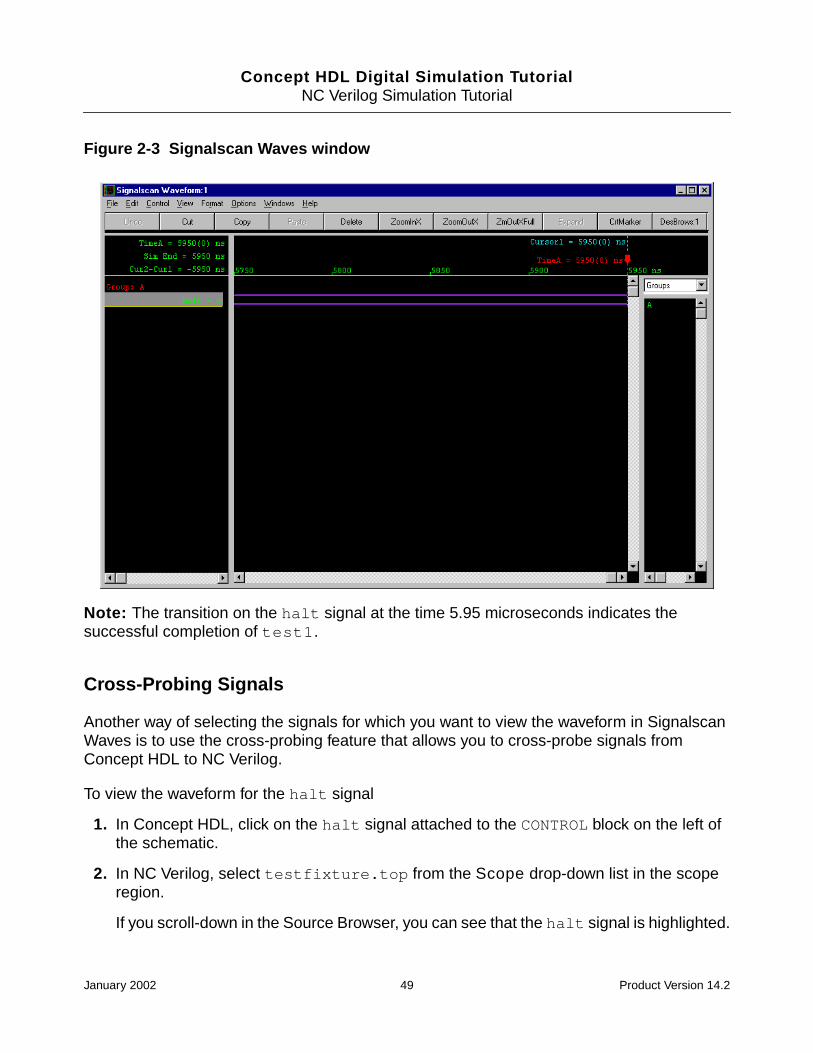
Figure 1-3 Signalscan Waves window
Note: The transition on the halt signal at the time 5.95 microseconds indicates thesuccessful completion of test1.
Cross-Probing Signals
Another way of selecting the signals for which you want to view the waveform in SignalscanWaves is to use the cross-probing feature that allows you to cross-probe signals fromConcept HDL to Verilog-XL.
To view the waveform for the halt signal
1. In Concept HDL, click on the halt signal attached to the CONTROL block on the left ofthe schematic.
2. In Verilog-XL, select risccpu from the Scope drop-down list in the scope region.
You can see that the halt signal is highlighted.
3. From the Verilog-XL window, click the Waveform View icon on the toolbar.
January 2002 27 Product Version 14.2

Concept HDL Digital Simulation TutorialVerilog-XL Simulation Tutorial
The waveform for the halt signal is displayed in the Signalscan Waves window (seeFigure 1-3 on page 27).
You have now completed the tutorial.
You can try out running the diagnostic programs test2, and test3 and view the waveforms.
■ The test2 diagnostic program tests the advanced instruction set of the VeriRisc system.If the system executes each instruction correctly, then it should halt when the HLTinstruction at address 10(hex) is executed. If the system halts at any other location, thenan instruction did not execute properly.
■ The test3 diagnostic program is an actual program that calculates the Fibonaccinumber sequence from 0 to 144. The Fibonacci number sequence is a series of numbersin which each number in the sequence is the sum of the preceding two numbers (that is,0, 1, 1, 2, 3, 5, 8, 13 ...). This number sequence is used in financial analysis.
When you are finished, select File > Exit in the SimControl window.
Summary
The Verilog simulation illustrated a high-level behavioral simulation using Verilog-XL withConcept HDL Digital Simulation Interface. All of the modules used in the design were definedas Verilog descriptions. A Verilog testfixture provided the stimulus. Waveforms were displayedusing Signalscan Waves.This type of simulation is common in the early phases of a design.
January 2002 28 Product Version 14.2

Concept HDL Digital Simulation Tutorial
2NC Verilog Simulation Tutorial
Overview
This tutorial demonstrates performing digital simulation in Concept HDL using the CadenceAffirma NC Verilog simulator. It walks you through the tasks involved in setting up theConcept HDL simulation interface for the NC Verilog simulator and performing digitalsimulation using the Cadence Affirma NC Verilog simulator.
After going through this tutorial, you will have a good understanding of the Concept HDL mapfile based simulation solution using the NC Verilog simulator and gain familiarity with thevarious tools used in the flow.
Figure 2-1 NC Verilog Simulation Flow
Concept HDL
Packager-XLSimulationHierarchy
Allegro/SigNoise
Editor Interface
Physicallayoutbinding
Design Netlist Design Netlist
Wire delaysfor timingverification
Packagerfiles
NC Verilog
library models,wire delays,stimulus andsimulator options
compilescriptSimulation netlist,
Verilogconfiguration
Create/edit
January 2002 29 Product Version 14.2

Concept HDL Digital Simulation TutorialNC Verilog Simulation Tutorial
Audience
This tutorial is for designers interested in simulating a schematic based mixed level designentered in Concept HDL. Familiarity with the Concept HDL schematic editor, Verilog HDL andthe Cadence Affirma NC Verilog simulator is assumed.
For more information, see the following documentation:
■ Concept HDL User Guide
■ Concept HDL Digital Simulation User Guide
■ Concept HDL Libraries Reference
■ Affirma NC Verilog Simulator Help
■ Affirma Simvision Analysis Environment User Guide
How to Use this Tutorial
This tutorial uses a design example to walk you through the tasks involved in performingdigital simulation in Concept HDL using the Cadence Affirma NC Verilog simulator. Youshould perform the tasks described in the tutorial in the sequence they appear.
Before using the tutorial you should install the design example database.
Installing the Design Example Database
A hierarchical design risccpu is used throughout this tutorial. To create a local copy of thedesign example database used in this tutorial, use the following procedure.
On UNIX
1. Open a UNIX shell window.
2. Change to the directory in which you want to install the design example database.
3. Copy the sim_ncvlog_des_ex.t.Z file located at your_install_dir/share/fet/examples/lwbhdl/ to the current directory.
The your_install_dir variable specifies the directory where you have installed theCadence PCB Design software. You can find the installation location by typingcds_root in a UNIX shell window.
January 2002 30 Product Version 14.2

Concept HDL Digital Simulation TutorialNC Verilog Simulation Tutorial
4. At the command prompt, execute the following command:
zcat sim_ncvlog_des_ex.t.Z | tar xvof -
This command creates a directory called sim_ncvlog_des_ex in the currentdirectory.
5. Change directory to the design example project directory.
cd sim_ncvlog_des_ex
6. Set the following environment variables:
❑ CONCEPT_INST_DIR to point to the directory where you have installed the CadencePCB Design software. For example, if you have installed the PSD software at /cdsinst/psd14, use the following command:
setenv CONCEPT_INST_DIR /cdsinst/psd14
❑ LDV_INST_DIR to point to the directory where you have installed the Cadence LDVsoftware. For example, if you have installed the LDV software at /cdsinst/ldv3,use the following command:
setenv LDV_INST_DIR /cdsinst/ldv3
On Windows NT
1. Browse to the directory:
your_install_dir\share\fet\examples\lwbhdl\
The your_install_dir variable specifies the directory where you have installed theCadence PCB Design software.
2. Unzip the sim_ncvlog_des_ex.zip file using WinZip to the directory where you wantto install the design example database. A directory called sim_ncvlog_des_ex iscreated.
3. Set the following environment variables:
❑ CONCEPT_INST_DIR to point to the directory where you have installed the CadencePCB Design software. For example, if you have installed the PSD software atC:\PSD14, set the CONCEPT_INST_DIR environment variable to point to thatlocation.
❑ LDV_INST_DIR to point to the directory where you have installed the Cadence LDVsoftware. For example, if you have installed the LDV software at C:\LDV3, set theLDV_INST_DIR environment variable to point to that location.
January 2002 31 Product Version 14.2

Concept HDL Digital Simulation TutorialNC Verilog Simulation Tutorial
Digital Simulation Overview
Digital simulation in Concept HDL using the NC Verilog simulator involves the following tasks.These tasks are explained in more detail throughout this tutorial.
1. Setting up the Project on page 32
2. Setting up the options for netlisting, compiling, and simulation in the simulation interfacefor the NC Verilog simulator. For more information, see Setting Up the SimulationInterface for NC Verilog on page 35.
3. Providing Stimulus for the Design on page 41
4. Simulating the design and viewing the results. You can perform cross probing betweenConcept HDL and NC Verilog to quickly debug your design. For more information, seeRunning the NC Verilog Simulator on page 42, and Simulating the Design on page 46.
Setting up the Project
In this section you will open the design example project in the Project Manager tool. You willthen invoke the Project Setup window to setup the following:
■ Selecting the NC Verilog simulator
■ Selecting the root design view for Verilog simulation
■ Selecting the default design configuration view for Verilog simulation
To setup the project
1. Invoke Project Manager.
2. Choose File > Open and browse to select the project file cpu.cpm located in thesim_ncvlog_des_ex directory.
January 2002 32 Product Version 14.2

Concept HDL Digital Simulation TutorialNC Verilog Simulation Tutorial
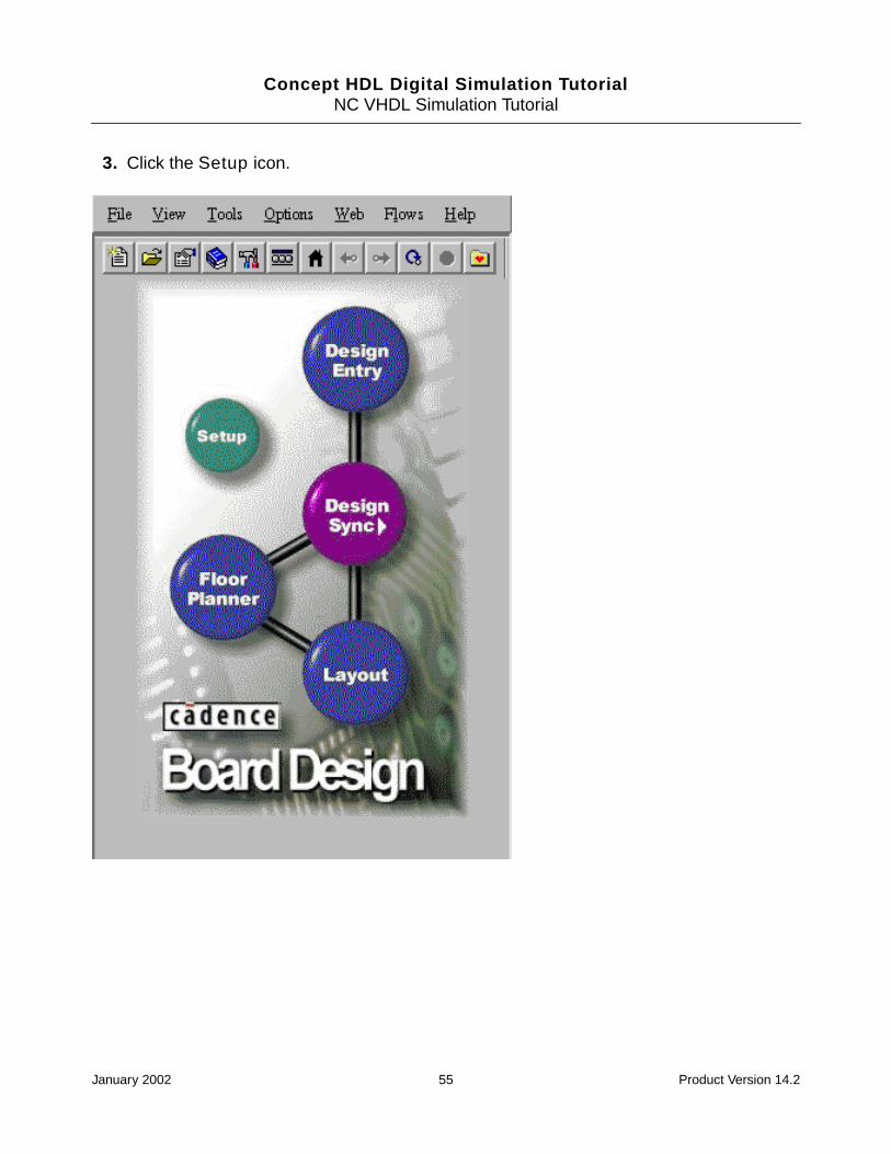
3. Click the Setup icon.
January 2002 33 Product Version 14.2

Concept HDL Digital Simulation TutorialNC Verilog Simulation Tutorial
The Project Setup window appears.
For more information on the Project Setup window, see the Project Setup OnlineHelp.
4. Select the Tools tab and click on the Simulation Setup button.
The Choose Simulator dialog box appears.
5. Select NC Verilog and click OK.
6. Select the Views tab and set the root design view for Verilog Simulation as sim_sch_1.
7. Select the Expansion tab and select the Verilog Simulation option.
8. Click on the Browse button against the Verilog Simulation option and select thecfg_verilog view. The cfg_verilog view will be used as the default configurationview for Verilog simulation.
9. Click OK.
January 2002 34 Product Version 14.2

Concept HDL Digital Simulation TutorialNC Verilog Simulation Tutorial
Opening the Design in Concept HDL
You will now open the design in the Concept HDL schematic editor.
➤ In Project Manager, click on the Design Entry icon.
Concept HDL appears and displays the following risccpu design. For more informationon using Concept HDL see the Concept HDL User Guide.
This design is a 2-1 risccpu. Other than a RESET signal, the design is self-stimulating.Programs are loaded into the memory and the program runs the CPU until successfulcompletion when the HALT signal is set.
All the modules in the design have Verilog descriptions. Many of these modules haveschematic descriptions as well. The board-level components have simulation models, whichcan run in NC Verilog.
Setting Up the Simulation Interface for NC Verilog
Before simulating the design you have to specify the options for netlisting, compiling,elaboration and simulation in the Concept HDL simulation interface for the NC Verilogsimulator.
January 2002 35 Product Version 14.2

Concept HDL Digital Simulation TutorialNC Verilog Simulation Tutorial
In this section you will setup the simulation interface for NC Verilog. For more information onthe simulation interface for NC Verilog, see the online help and the Concept HDL DigitalSimulation User Guide.
To invoke the simulation interface for NC Verilog
1. In Concept HDL, choose Tools > Simulate.
The NC Verilog start simulator dialog box appears.
The simulation interface appears with cfg_verilog as the design configuration viewfor Verilog simulation. By default, a run directory sim1 is created under the configurationview you have selected. This directory contains the log and marker files that aregenerated when you run the simulation.
2. Click the Setup button to invoke the NC Verilog setup dialog box.
Specifying the Verilog Netlisting Options
This section introduces you to the interface where you can specify the options for netlistingthe design. For more information, see the online help and the Concept HDL DigitalSimulation User Guide.
January 2002 36 Product Version 14.2

Concept HDL Digital Simulation TutorialNC Verilog Simulation Tutorial
To specify the Verilog netlisting options
1. Select the Netlist tab in the NC Verilog setup dialog box.
By default the netlist will be regenerated every time you click Run in the NC Verilog startsimulator dialog box. If more than 50 errors are identified during the netlisting process,Concept HDL will not generate the netlist for the design. If you want to increase thenumber of acceptable netlisting errors in the design, specify the same in the Max Errorsfield.
2. Select the Verbose Output option.
The debug messages for the netlisting process will be displayed when you run thesimulation process.
January 2002 37 Product Version 14.2

Concept HDL Digital Simulation TutorialNC Verilog Simulation Tutorial
3. Select the Generate Compile Script option.
A compilescript file that lists all the components used in the design is created in therun directory. When the design is compiled, any local libraries you use in your designare automatically compiled by running the compilescript file.
Note: If any library used in your design is un-compiled, you cannot compile your designusing NC Verilog.
Setting Up the NC Verilog Simulator Options
This section introduces you to the interface where you can specify the options for running theNC Verilog simulator. For more information, see the online help and the Concept HDLDigital Simulation User Guide.
To setup the options for running the NC Verilog simulator
1. Select the Simulation tab in the NC Verilog setup dialog box.
January 2002 38 Product Version 14.2

Concept HDL Digital Simulation TutorialNC Verilog Simulation Tutorial
You can specify the options for running the NC Verilog simulator in this tab.
The hdl.var file field specifies the path to the hdl.var file that will be used for thesimulation. This is an ASCII text file that contains a definition of the WORK variable. TheWORK variable specifies the work library where the compiler stores compiled objects andother derived data.
If you do not specify the path to the hdl.var file, a default hdl.var file is created in therun directory.The contents of the default hdl.var file is given below:
DEFINE work lwb_des_ex
DEFINE NCVLOGOPTS -messages
DEFINE NCELABOPTS -messages
DEFINE NCSIMOPTS -messages
The DEFINE work lwb_des_ex statement indicates that the compiled objects andother derived data will be stored in the lwb_des_ex library of the design. See theAffirma NC Verilog Simulator Help for details on the hdl.var file.
The following log files will be created in the specified log directory when you run thesimulation process:
January 2002 39 Product Version 14.2

Concept HDL Digital Simulation TutorialNC Verilog Simulation Tutorial
❑ ncvlog.log, which contains the messages logged when the design is compiled.
❑ ncelab.log, which contains the messages logged when the design is elaborated.
❑ ncsim.log, which contains the messages logged when the design is simulated.
Note: By default the log files are created in the run directory.
2. Select the Compile, Elaborate, and Simulate check boxes.
You can specify command line options for ncvlog, ncelab and ncsim respectively inthe Cmd Options field against the Compile, Elaborate, and Simulate check boxes.
The design will be compiled, elaborated, and simulated every time you run the simulationprocess.
The Start SimVision check box that is selected by default indicates that NC Verilog will beinvoked in the Affirma SimVision analysis and debug environment. For more information, seethe Affirma Simvision Environment User Guide. The Enter Interactive Mode check boxthat is also selected by default indicates that NC Verilog is stopped at time 0 for you to specifythe stimulus.
January 2002 40 Product Version 14.2

Concept HDL Digital Simulation TutorialNC Verilog Simulation Tutorial
Providing Stimulus for the Design
This section introduces you to the interface where you can provide the stimulus for the design.For more information, see the online help and the Concept HDL Digital Simulation UserGuide.
In this tutorial, the stimulus file is provided with the design example. For Verilog simulation,the stimulus is provided by a Verilog testfixture. This testfixture provides interactive tasks forprogramming the memory and displaying circuit activity for several nets.
To provide the stimulus for the design
1. Select the Stimulus tab in the NC Verilog setup dialog box.
The Stimulus tab allows you to generate a testbench or include a previously createdtestbench.
January 2002 41 Product Version 14.2

Concept HDL Digital Simulation TutorialNC Verilog Simulation Tutorial
2. Select the Include Test Bench option.
3. Click Browse to select the verilog.v file in the /sim_ncvlog_des_ex/lwb_des_ex/testfixture/risccpu_sim_sch_1/ directory. This file enables youto run three tests on the risccpu design during the simulation.
4. Click OK to save the options specified in the simulation interface.
The NC Verilog start simulator dialog box appears.
You are now ready to simulate the design.
Running the NC Verilog Simulator
This section describes the procedures you need to follow to run the NC Verilog simulator fromthe Concept HDL digital simulation interface, and selecting the signals to be monitored whenthe simulation is run on the design.
This section describes the procedures you need to follow to simulate the sample circuit.
Starting NC Verilog in the SimVision Environment
1. In the NC Verilog start simulator dialog box, click on the Run button.
January 2002 42 Product Version 14.2

Concept HDL Digital Simulation TutorialNC Verilog Simulation Tutorial
The Simulation Progress Status window appears.
2. Click on the Details button to view the details of the simulation process.
The Verilog netlist for each component in the hierarchy bound to the sim_sch_1 view isgenerated.
The Verilog netlist for each component bound to the sim_sch_1 view is generated.Once the netlist is generated, the Verilog source files are compiled by running thencvlog program. The ncvlog program performs syntactic and static semantic checkingon the input source files or Verilog design units. If no errors are found, compilationproduces an internal representation for each HDL design unit in the source files. See“Compiling Verilog Source Files with ncvlog” in the Affirma NC Verilog SimulatorHelp for details on ncvlog.
After compiling the Verilog source code, the design is elaborated using a program calledncelab. The elaboration process constructs a design hierarchy based on theinstantiation and configuration information in the design, establishes signal connectivity,and computes initial values for all objects in the design. This design hierarchy is storedin a simulation snapshot.
At the end of the elaboration process, ncelab writes out a simulation snapshot calledwork.testfixture:cfg_verilog\verilog.v. This snapshot is the representationof your design that the NC Verilog simulator uses to run the simulation.
Once the design is netlisted, compiled, and elaborated, NC Verilog is invoked in theSimControl window (see Figure 2-2 on page 45) of the Affirma SimVision analysis anddebug environment.
January 2002 43 Product Version 14.2

Concept HDL Digital Simulation TutorialNC Verilog Simulation Tutorial
The Affirma SimVision Analysis Environment
The Affirma SimVision analysis environment is a unified graphical debug environment forCadence simulators. The SimVision environment features advanced debug and analysistools and innovative high-level design and visualization capabilities. These tools include:
■ The SimControl window (see Figure 2-2 on page 45), which allows you to directlyinteract with the simulator. You can single step, trace signals, set breakpoints, andobserve signals to verify your designs. SimControl also provides access to the followingdebug tools:
■ The Watch Objects window, which lets you observe the value of selected signals.
■ The Navigator window, which displays the design hierarchy and shows you signalvalues at any level of the hierarchy.
■ Signalscan Waves (see Figure 2-3 on page 49), which lets you display waveforms.
■ Comparescan, which lets you compare SHM and VCD waveform databases.
See the SimVision Analysis Environment User Guide for details on the SimVisionanalysis environment.
The SimControl Window
SimControl is the main SimVision analysis environment window. The following figure showsthe SimControl window as it appears when the simulator is invoked using the tutorialexample:
January 2002 44 Product Version 14.2

Concept HDL Digital Simulation TutorialNC Verilog Simulation Tutorial
Figure 2-2 SimControl window
The different parts of the SimControl window are briefly explained below:
■ The Tool Bar, which contains buttons that give you fast access to commonly-usedcommands and to the other SimVision tools. You can define your own buttons for Tclcommands and add them to the tool bar.
■ The Source Browser, which displays your source code. You can select scopes, signals,or ports in the Source Browser and operate on them.
■ The Scope Region, which displays the current scope and allows you to quickly set thescope to another level in the hierarchy.
■ The Input/Output Region, which displays simulator output and allows command-lineinput to the simulator.
Tool Bar
SourceBrowser
ScopeRegion
SimulatorInput/OutputRegion
January 2002 45 Product Version 14.2

Concept HDL Digital Simulation TutorialNC Verilog Simulation Tutorial
Simulating the Design
This section describes the procedures for simulating the design and viewing the results. Italso gives an overview of the cross-probing of signals between Concept HDL and NC Verilog.
1. Switch to the SimControl window (see Figure 2-2 on page 45).
Notice that in the toolbar, Time displayed is 0. This indicates that NC Verilog is stoppedat time 0 for you to specify the stimulus.
2. Click the Run Simulation icon in the toolbar.
NC Verilog executes the Verilog testfixture (/sim_ncvlog_des_ex/lwb_des_ex/testfixture/risccpu_sim_sch_1/verilog.v) and prompts you to run threediagnostic programs, test1, test2, and test3.
NC Verilog waits for your input because the Verilog testfixture schedules a $stop atsimulation time 0.
3. In the C1> prompt, type the following command and press Enter:
task testfixture.test1;
This command invokes the user-defined Verilog task test1that loads the memory. Thetest1 diagnostic program tests the basic instruction set of the VeriRisc system. If thesystem executes each instruction correctly, it should halt when the HALT instruction ataddress 17(hex) is executed. If the system halts at any other location, then an instructiondid not execute properly.
4. Click the Run Simulation icon in the toolbar.
5. Click again on the Run Simulation icon in the NC Verilog toolbar.
The HALT instruction is encountered at time 5.95 microseconds. NC Verilog resets totime 0 and prompts you to run one of the three diagnostic tests.
January 2002 46 Product Version 14.2

Concept HDL Digital Simulation TutorialNC Verilog Simulation Tutorial
Viewing Simulation Results
This section describes the procedures for displaying the results of the Verilog behavioralsimulation. You use Signalscan Waves to view and analyze the results.
January 2002 47 Product Version 14.2

Concept HDL Digital Simulation TutorialNC Verilog Simulation Tutorial
1. Use the scroll bar in the Source Browser to go to line 76.
2. Right-click on halt, and choose Wave Trace.
The waveform for the halt signal is displayed in the Signalscan Waves window.
January 2002 48 Product Version 14.2
Concept HDL Digital Simulation TutorialNC Verilog Simulation Tutorial
Figure 2-3 Signalscan Waves window
Note: The transition on the halt signal at the time 5.95 microseconds indicates thesuccessful completion of test1.
Cross-Probing Signals
Another way of selecting the signals for which you want to view the waveform in SignalscanWaves is to use the cross-probing feature that allows you to cross-probe signals fromConcept HDL to NC Verilog.
To view the waveform for the halt signal
1. In Concept HDL, click on the halt signal attached to the CONTROL block on the left ofthe schematic.
2. In NC Verilog, select testfixture.top from the Scope drop-down list in the scoperegion.
If you scroll-down in the Source Browser, you can see that the halt signal is highlighted.
January 2002 49 Product Version 14.2

Concept HDL Digital Simulation TutorialNC Verilog Simulation Tutorial
3. From the NC Verilog window, click the Waveform View icon on the toolbar.
The waveform for the halt signal is displayed in the Signalscan Waves window (seeFigure 2-3 on page 49).
You have now completed the tutorial.
You can try out running the diagnostic programs test2, and test3 and view the waveforms.
■ The test2 diagnostic program tests the advanced instruction set of the VeriRisc system.If the system executes each instruction correctly, then it should halt when the HLTinstruction at address 10(hex) is executed. If the system halts at any other location, thenan instruction did not execute properly.
■ The test3 diagnostic program is an actual program that calculates the Fibonaccinumber sequence from 0 to 144. The Fibonacci number sequence is a series of numbersin which each number in the sequence is the sum of the preceding two numbers (that is,0, 1, 1, 2, 3, 5, 8, 13 ...). This number sequence is used in financial analysis.
When you are finished, select File > Exit in the SimControl window.
Summary
The Verilog simulation illustrated a high-level behavioral simulation using NC Verilog withConcept HDL Digital Simulation Interface. All of the modules used in the design were definedas Verilog descriptions. A Verilog testfixture provided the stimulus. Waveforms were displayedusing Signalscan Waves.This type of simulation is common in the early phases of a design.
January 2002 50 Product Version 14.2

Concept HDL Digital Simulation Tutorial
3NC VHDL Simulation Tutorial
Overview
This tutorial demonstrates performing digital simulation in Concept HDL using the CadenceAffirma NC VHDL simulator. It walks you through the tasks involved in setting up theConcept HDL simulation interface for the NC VHDL simulator and performing digitalsimulation using the Cadence Affirma NC VHDL simulator.
After going through this tutorial, you will have a good understanding of the Concept HDLwrapper file based simulation solution using the NC VHDL simulator and gain familiarity withthe various tools used in the flow.
Figure 3-1 NC VHDL Simulation Flow
Concept HDL
Packager-XLSimulationHierarchy
Allegro/SigNoise
Editor Interface
Physicallayoutbinding
Verilog Netlist VHDL Netlist
Wire delaysfor timingverification
Packagerfiles
NC VHDL
wire delays,stimulus and options for compiler,elaborator andsimulator
Compilescript
VHDLconfiguration
Create/edit
January 2002 51 Product Version 14.2

Concept HDL Digital Simulation TutorialNC VHDL Simulation Tutorial
Audience
This tutorial is for designers interested in simulating a schematic based mixed level designentered in Concept HDL. Familiarity with the Concept HDL schematic editor, VHDL and theCadence Affirma NC VHDL simulator is assumed.
For more information, see the following documentation:
■ Concept HDL User Guide
■ Concept HDL Digital Simulation User Guide
■ Concept HDL Libraries Reference
■ Affirma NC VHDL Simulator Help
■ Affirma Simvision Analysis Environment User Guide
How to Use this Tutorial
This tutorial uses a design example to walk you through the tasks involved in performingdigital simulation in Concept HDL using the Cadence Affirma NC Verilog simulator. Youshould perform the tasks described in the tutorial in the sequence they appear.
Before using the tutorial you should install the design example database.
Installing the Design Example Database
The design example used throughout this tutorial is a simple counter circuit. To create alocal copy of the design example database, use the following procedure.
On UNIX
1. Open a UNIX shell window.
2. Change to the directory in which you want to install the design example database.
3. Copy the sim_ncvhdl_des_ex.t.Z file located at your_install_dir/share/fet/examples/lwbhdl/ to the current directory.
The your_install_dir variable specifies the directory where you have installed theCadence PCB Design software. You can find the installation location by typingcds_root in a UNIX shell window.
January 2002 52 Product Version 14.2

Concept HDL Digital Simulation TutorialNC VHDL Simulation Tutorial
4. At the command prompt, execute the following command:
zcat sim_ncvhdl_des_ex.t.Z | tar xvof -
This command creates a directory called sim_ncvhdl_des_ex in the currentdirectory.
5. Change directory to the design example project directory.
cd sim_ncvhdl_des_ex
6. Set the following environment variables:
❑ CONCEPT_INST_DIR to point to the directory where you have installed the CadencePSD software. For example, if you have installed the PSD software at /cdsinst/psd14, use the following command:
setenv CONCEPT_INST_DIR /cdsinst/psd14
❑ LDV_INST_DIR to point to the directory where you have installed the Cadence LDVsoftware. For example, if you have installed the LDV software at /cdsinst/ldv3,use the following command:
setenv LDV_INST_DIR /cdsinst/ldv3
On Windows NT
1. Browse to the directory:
your_install_dir\share\fet\examples\lwbhdl\
The your_install_dir variable specifies the directory where you have installed theCadence PCB Design software.
2. Unzip the sim_ncvhdl_des_ex.zip file using WinZip to the directory where you wantto install the design example database. A directory called sim_ncvhdl_des_ex iscreated.
3. Set the following environment variables:
❑ CONCEPT_INST_DIR to point to the directory where you have installed the CadencePSD software. For example, if you have installed the PSD software at C:\PSD14,set the CONCEPT_INST_DIR environment variable to point to that location.
❑ LDV_INST_DIR to point to the directory where you have installed the Cadence LDVsoftware. For example, if you have installed the LDV software at C:\LDV3, set theLDV_INST_DIR environment variable to point to that location.
January 2002 53 Product Version 14.2
Concept HDL Digital Simulation TutorialNC VHDL Simulation Tutorial
Digital Simulation Overview
Digital simulation in Concept HDL using the NC VHDL simulator involves the following tasks.These tasks are explained in more detail throughout this tutorial.
1. Setting up the Project on page 54
2. Setting up the options for netlisting, compiling, elaboration, and simulation in thesimulation interface for the NC VHDL simulator. For more information, see Setting Up theSimulation Interface for NC VHDL on page 58.
3. Providing Testfixture for the Design on page 62
4. Simulating the design and viewing the results. You can perform cross probing betweenConcept HDL and NC VHDL to quickly debug your design. For more information, seeRunning the NC VHDL Simulator on page 64 and Simulating the Design on page 72.
Setting up the Project
In this section you will open the design example project in the Project Manager tool. You willthen invoke the Project Setup window to setup the following:
■ Selecting the NC VHDL simulator
■ Selecting the root design view for VHDL simulation
■ Selecting the default design configuration view for VHDL simulation
To setup the project
1. Invoke Project Manager.
2. Choose File >Open and browse to select the project file count.cpm located in thesim_ncvhdl_des_ex directory.
January 2002 54 Product Version 14.2
Concept HDL Digital Simulation TutorialNC VHDL Simulation Tutorial
3. Click the Setup icon.
January 2002 55 Product Version 14.2

Concept HDL Digital Simulation TutorialNC VHDL Simulation Tutorial
The Project Setup window appears.
For more information on the Project Setup window, see the Project Setup OnlineHelp.
4. Select the Tools tab and click on the Simulation Setup button.
The Choose Simulator dialog box appears.
5. Select NC VHDL and click OK.
6. Select the Views tab and set the root design view for VHDL Simulation as sim_sch_1.
7. Select the Expansion tab and select the VHDL Simulation option.
8. Click on the Browse button against the VHDL Simulation option and select thecfg_vhdl view. The cfg_vhdl view will be used as the default configuration view forVHDL simulation.
9. Click on the Edit button against the VHDL Simulation expansion type option toconfigure the cfg_vhdl design configuration view.
January 2002 56 Product Version 14.2

Concept HDL Digital Simulation TutorialNC VHDL Simulation Tutorial
10. Click OK.
Opening the Design in Concept HDL
You will now open the design in the Concept HDL schematic editor.
➤ In Project Manager, click on the Design Entry icon.
Concept HDL appears and displays the sysctrl design. For more information on usingConcept HDL see the Concept HDL User Guide.
This sysctrl design will be used to illustrate the Concept HDL digital simulation flow.
January 2002 57 Product Version 14.2

Concept HDL Digital Simulation TutorialNC VHDL Simulation Tutorial
Setting Up the Simulation Interface for NC VHDL
Before simulating the design you have to specify the options for netlisting, compiling,elaboration and simulation in the Concept HDL simulation interface for the NC VHDLsimulator.
In this section you will setup the simulation interface for NC VHDL. For more information onthe simulation interface for NC VHDL, see the online help and the Concept HDL DigitalSimulation User Guide.
To invoke the simulation interface for NC VHDL
1. In Concept HDL, choose Tools -> Simulate.
The NC VHDL start simulator dialog box appears.
The simulation interface appears with cfg_vhdl as the design configuration view forVHDL simulation. By default, a run directory sim1 is created under the configurationview you have selected. This directory contains the log and marker files that aregenerated when you run the simulation.
2. Click the Setup button to invoke the NC VHDL setup dialog box.
Specifying the VHDL Netlisting Options
This section introduces you to the interface where you can specify the options for netlistingthe design. For more information, see the online help and the Concept HDL DigitalSimulation User Guide.
January 2002 58 Product Version 14.2

Concept HDL Digital Simulation TutorialNC VHDL Simulation Tutorial
To specify the VHDL netlisting options
1. Select the Netlist tab in the NC VHDL setup dialog box.
You can specify the options for generating the VHDL netlist in this tab.
2. Select the Regenerate Netlist option.
3. Select the Generate Compile Script option.
A compilescript file that lists all the components used in the design is created in therun directory. When the design is compiled, any local libraries you use in your designare automatically compiled by running the compilescript file.
Note: If any library used in your design is un-compiled, you cannot compile your design
January 2002 59 Product Version 14.2

Concept HDL Digital Simulation TutorialNC VHDL Simulation Tutorial
using NC VHDL.
Setting Up the NC VHDL Simulator Options
This section introduces you to the interface where you can specify the options for running theNC VHDL simulator. For more information, see the online help and the Concept HDL DigitalSimulation User Guide.
To setup the options for running the NC VHDL simulator
1. Select the Simulation tab in the NC VHDL setup dialog box.
You can specify the options for running the NC VHDL simulator in this tab.
The hdl.var file field specifies the path to the hdl.var file that will be used for thesimulation. This is an ASCII text file that contains a definition of the WORK variable. TheWORK variable specifies the work library where the compiler stores compiled objects andother derived data.
January 2002 60 Product Version 14.2

Concept HDL Digital Simulation TutorialNC VHDL Simulation Tutorial
If you do not specify the path to the hdl.var file, a default hdl.var file is created in therun directory.The contents of the default hdl.var file is given below:
DEFINE work sysctrl_lib
DEFINE NCVHDLOPTS -messages
DEFINE NCELABOPTS -messages
DEFINE NCSIMOPTS -messages
The DEFINE work sysctrl_lib statement indicates that the compiled objects andother derived data will be stored in the sysctrl library of the design. See the AffirmaNC VHDL Simulator Help for details on the hdl.var file.
The following log files will be created in the specified log directory when you run thesimulation process:
❑ ncvhdl.log, which contains the messages logged when the design is compiled.
❑ ncelab.log, which contains the messages logged when the design is elaborated.
❑ ncsim.log, which contains the messages logged when the design is simulated.
Note: By default the log files are created in the run directory.
2. Select the Compile, Elaborate, and Simulate check boxes.
You can specify command line options for ncvlog, ncelab, and ncsim respectively inthe Cmd Options field against the Compile, Elaborate, and Simulate check boxes.
The design will be compiled, elaborated, and simulated every time you run the simulationprocess.
The Start SimVision check box that is selected by default indicates that NC VHDL will beinvoked in the Affirma SimVision analysis and debug environment. For more information, seethe Affirma Simvision Environment User Guide. The Enter Interactive Mode check boxthat is also selected by default indicates that NC VHDL is stopped at time 0 for you to specifythe stimulus.
January 2002 61 Product Version 14.2
Concept HDL Digital Simulation TutorialNC VHDL Simulation Tutorial
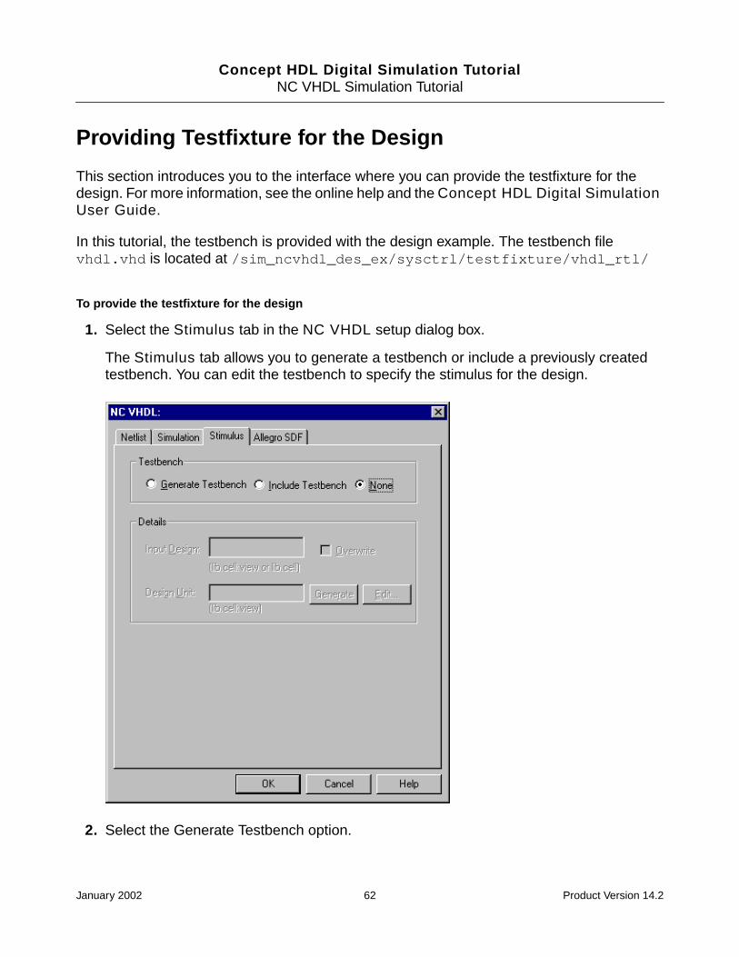
Providing Testfixture for the Design
This section introduces you to the interface where you can provide the testfixture for thedesign. For more information, see the online help and the Concept HDL Digital SimulationUser Guide.
In this tutorial, the testbench is provided with the design example. The testbench filevhdl.vhd is located at /sim_ncvhdl_des_ex/sysctrl/testfixture/vhdl_rtl/
To provide the testfixture for the design
1. Select the Stimulus tab in the NC VHDL setup dialog box.
The Stimulus tab allows you to generate a testbench or include a previously createdtestbench. You can edit the testbench to specify the stimulus for the design.
2. Select the Generate Testbench option.
January 2002 62 Product Version 14.2

Concept HDL Digital Simulation TutorialNC VHDL Simulation Tutorial
3. Type sysctrl_lib.sysctrl in the Input Design field to specify the VHDL entityarchitecture for which you want to generate the testbench.
You can specify the VHDL entity architecture for which you want to generate thetestbench in the lib.cell or lib.cell:view format.
4. Type sysctrl_lib.testfixture:vhdl_rtl in the Design Unit field to specify thedesign view where you want to create the testbench.
5. Click Generate to generate the testbench file vhdl.vhd in the design view.
6. Click Edit.
The testbench file is opened in a text editor.
7. Specify the stimulus for the design as below:
reset_n <= ’1’ after 5 ns,
’0’ after 290 ns,
’1’ after 320 ns;
preset_n <= ’1’ after 10 ns,
’0’ after 35 ns,
’1’ after 70 ns,
’0’ after 635 ns,
’1’ after 670 ns;
clock_n <= ’0’ after 50 ns,
’1’ after 100 ns,
’0’ after 150 ns,
’1’ after 200 ns,
’0’ after 250 ns,
’1’ after 300 ns,
’0’ after 350 ns,
’1’ after 400 ns,
’0’ after 450 ns,
’1’ after 500 ns,
’0’ after 550 ns,
’1’ after 600 ns,
’0’ after 650 ns,
’1’ after 700 ns,
’1’ after 750 ns;
See the sample stim.vhd file located in the /sim_ncvhdl_des_ex/ directory toknow how the stimulus is specified in the testbench file.
January 2002 63 Product Version 14.2

Concept HDL Digital Simulation TutorialNC VHDL Simulation Tutorial
8. Save the testbench file and close the text editor.
9. Click OK to save the options specified in the simulation interface.
The NC VHDL start simulator dialog box appears.
You are now ready to simulate the design.
Running the NC VHDL Simulator
This section describes the procedures you need to follow to run the NC VHDL simulator fromthe Concept HDL digital simulation interface, and selecting the signals to be monitored whenthe simulation is run on the counter design.
Starting NC VHDL in the SimVision Environment
1. In the NC VHDL start simulator dialog box, click on the Run button.
January 2002 64 Product Version 14.2

Concept HDL Digital Simulation TutorialNC VHDL Simulation Tutorial
The Simulation Progress Status window appears.
2. Click on the Details button to view the details of the simulation process.
The VHDL netlist for each component bound to the sim_sch_1 view is generated.Once the netlist is generated, the VHDL source files are compiled by running the ncvhdlprogram. The ncvhdl program performs syntactic and static semantic checking on theinput source files or VHDL design units. If no errors are found, compilation produces aninternal representation for each HDL design unit in the source files. See “CompilingVHDL Source Files With ncvhdl” in the Affirma NC VHDL Simulator Help for detailson ncvhdl.
After compiling the VHDL source code, the design is elaborated using a program calledncelab. The elaboration process constructs a design hierarchy based on theinstantiation and configuration information in the design, establishes signal connectivity,and computes initial values for all objects in the design. This design hierarchy is storedin a simulation snapshot.
At the end of the elaboration process, ncelab writes out a simulation snapshot calledwork.testgixture:cfg_vhdl. This snapshot is the representation of your designthat the NC VHDL simulator uses to run the simulation.
Once the design is netlisted, compiled, and elaborated, NC VHDL is invoked in theSimControl window (see Figure 3-2 on page 67) of the Affirma SimVision analysis anddebug environment.
January 2002 65 Product Version 14.2

Concept HDL Digital Simulation TutorialNC VHDL Simulation Tutorial
The Affirma SimVision Analysis Environment
The Affirma SimVision analysis environment is a unified graphical debug environment forCadence simulators. The SimVision environment features advanced debug and analysistools and innovative high-level design and visualization capabilities. These tools include:
■ The SimControl window (see Figure 3-2 on page 67), which allows you to directlyinteract with the simulator. You can single step, trace signals, set breakpoints, andobserve signals to verify your designs. SimControl also provides access to the followingdebug tools:
■ The Watch Objects window (see Figure 3-4 on page 71), which lets you observe thevalue of selected signals.
■ The Navigator window (see Figure 3-3 on page 69), which displays the design hierarchyand shows you signal values at any level of the hierarchy.
■ Signalscan Waves (see Figure 3-5 on page 72), which lets you display waveforms.
■ Comparescan, which lets you compare SHM and VCD waveform databases.
See the SimVision Analysis Environment User Guide for details on the SimVisionanalysis environment.
The SimControl Window
SimControl is the main SimVision analysis environment window. The following figure showsthe SimControl window as it appears when the simulator is invoked using the tutorialexample:
January 2002 66 Product Version 14.2

Concept HDL Digital Simulation TutorialNC VHDL Simulation Tutorial
Figure 3-2 .SimControl window
The different parts of the SimControl window are briefly explained below:
■ The Tool Bar, which contains buttons that give you fast access to commonly-usedcommands and to the other SimVision tools. You can define your own buttons for Tclcommands and add them to the tool bar.
■ The Source Browser, which displays your source code. You can select scopes, signals,or ports in the Source Browser and operate on them.
■ The Scope Region, which displays the current scope and allows you to quickly set thescope to another level in the hierarchy.
■ The Input/Output Region, which displays simulator output and allows command-lineinput to the simulator.
Tool Bar
SourceBrowser
ScopeRegion
SimulatorInput/OutputRegion
January 2002 67 Product Version 14.2

Concept HDL Digital Simulation TutorialNC VHDL Simulation Tutorial
At this point, you can run the simulation by clicking the Run Simulation button .However, before we simulate the design, let’s look at a few important features of the AffirmaSimVision analysis environment.
Navigating the Design and Selecting Signals to Monitor
1. In the SimControl window, select Tools > Navigator or click on the Navigator iconon the tool bar.
The Navigator window appears.
2. Double-click on the folder icon in the left pane to expand the hierarchy (see Figure 3-3on page 69).
January 2002 68 Product Version 14.2

Concept HDL Digital Simulation TutorialNC VHDL Simulation Tutorial
Figure 3-3 Navigator window
You will notice that all top level objects with their values are displayed in the Object List.
The different parts of the SimControl window are briefly explained below:
❑ Scope Tree View, in which you can view your current design hierarchy in agraphical tree representation. To browse the hierarchy, double-click on a node toexpand to the lower level.
❑ Objects List, which displays a list of objects with their current simulation values anddeclarations.
❑ Object Filter, which controls the signals that are displayed in this window.
CurrentscopeObjectfilter
ObjectList
ScopeTreeView
HierarchyPath
January 2002 69 Product Version 14.2

Concept HDL Digital Simulation TutorialNC VHDL Simulation Tutorial
3. Click on the top icon in the Scope Tree View.
The current scope changes to :top and the Objects List displays the components andsignals for the top design instance. You will also notice that the Source Browser,Scope Region and Simulator Input/Output Region in the SimControl window (seeFigure 3-2 on page 67) get updated to reflect the current scope.
Note: If you change the scope in the SimControl window, the display in the Navigatorwindow gets updated to reflect the current scope.
4. Select the following signals:
January 2002 70 Product Version 14.2

Concept HDL Digital Simulation TutorialNC VHDL Simulation Tutorial
❑ \out\
❑ CLOCK
❑ PRESET
❑ RESET
Click the \out\ signal, press the CTRL key, and select the other signals.
5. Click the Watch window icon on the Navigator tool bar.
The Watch window appears. The four signals that you want to monitor during thesimulation are displayed in the window.
Figure 3-4 Watch window
Viewing Signals in SignalScan Waves
➤ In the Watch window, click the Waveform View icon on the toolbar.
This opens a SHM database called waves, probes the selected signals to the database,and invokes the Signalscan Waves window with all of the selected signals displayed.
January 2002 71 Product Version 14.2

Concept HDL Digital Simulation TutorialNC VHDL Simulation Tutorial
Figure 3-5 Signal Scan Waves window
Look at the SimControl window. Each Tcl command that you have executed using theSimVision windows is echoed in the simulator Input/Output region.
A scope command was executed whenever you changed the scope. The waveformdatabase was created with the database command, and the signals were added to thewaveform database with the probe command.
You are now ready to simulate the design.
Simulating the Design
This section describes the procedures for simulating the design and viewing the results. Italso gives an overview of the cross-probing of signals and component instances betweenConcept HDL and NC VHDL.
1. Switch to the SimControl window (see Figure 3-2 on page 67).
January 2002 72 Product Version 14.2

Concept HDL Digital Simulation TutorialNC VHDL Simulation Tutorial
Notice that in the toolbar, Time displayed is 0. This indicates that NC VHDL is stoppedat time 0 for you to specify the stimulus.
2. Click the Run Simulation icon in the toolbar.
Notice how the simulation time updates in the SimControl window just under the toolbar. Also notice that the waveforms update dynamically in the Signalscan Waveswindow as the simulation runs.The Watch window is updated when the simulation iscomplete. The Watch window displays the value of the signals after the simulation.
Viewing the Waveforms in Signalscan Waves
Once the simulation is complete, the Signalscan Waves window displays the updatedwaveforms for the signals. At this point, the waveform viewer is zoomed in to the end of thesimulation.
1. Click the ZmOutXFull button on the tool bar.
2. Click the ZoomInX button to zoom in until you can view the transitions on the signals.
To zoom in on a time region:
1. Select a signal transition. This inserts one cursor.
2. Insert a second cursor by clicking the middle mouse button (in UNIX) and the right mousebutton in Windows NT.
3. Click the ZoomInX button to zoom in between the cursors.
January 2002 73 Product Version 14.2

Concept HDL Digital Simulation TutorialNC VHDL Simulation Tutorial
Cross-probing between Concept HDL and NC VHDL
Cross-probing is an effective way of debugging a design. Through cross-probing you canselect a component or net in Concept HDL and view its value in NC VHDL using SimVisionor Signalscan Waves.This section describes the procedures for cross-probing signals andcomponent instances between Concept HDL and NC VHDL.
Cross-probing Signals
1. In Concept HDL, click on the PRESET signal at the top of the schematic.
The signal is highlighted in the source browser of the SimControl window (seeFigure 3-2 on page 67). Use the scroll bar in the source browser to view the highlightedsignal.
2. In the SimControl window, click the Waveform View icon on the toolbar. Thewaveform for the signal is displayed in the SignalScan window.
January 2002 74 Product Version 14.2

Concept HDL Digital Simulation TutorialNC VHDL Simulation Tutorial
Cross-probing Component Instances
1. In Concept HDL, click on the 74AC74 component instance on the right of the schematic.
The component instance is highlighted in the source browser of the SimControl window.Use the scroll bar in the source browser to view the highlighted component instance.
2. In the SimControl window, click the Waveform View icon on the toolbar. Thewaveform for all the signals in the scope of the component instance are opened inSignalScan window.
You have now completed the tutorial.
You can continue to experiment with the tools introduced in this tutorial. When you arefinished, select File > Exit in the SimControl window.
January 2002 75 Product Version 14.2

Concept HDL Digital Simulation TutorialNC VHDL Simulation Tutorial
January 2002 76 Product Version 14.2

Concept HDL Digital Simulation Tutorial
4Leapfrog Simulation Tutorial
This tutorial demonstrates performing digital simulation in Concept HDL using the CadenceLeapfrog VHDL simulator. This simulator is available only on UNIX platforms.
Audience
This document is targeted towards designers interested in simulating a schematic basedmixed level design entered in the Cadence Concept HDL schematic editor using the LeapfrogVHDL simulator.
For more information, see the following documentation:
■ Concept HDL User Guide
■ Concept HDL Digital Simulation User Guide
■ Concept HDL Libraries Reference
■ Leapfrog VHDL Simulator User Guide
■ Affirma Simvision Environment User Guide
System Simulation Process
The design process starts with Project Manager. Project Manager is an interface for theCadence board design solution. It is a tool for setting up projects and launching tools in a flow.The currently supported default flows are the Board Design flow and the Programmable ICflow. You can customize Project Manager flows.
As part of setting up the project, you choose libraries and various tool options. You canchoose the primary simulator from among:
■ Verilog-XL
■ Leapfrog
January 2002 77 Product Version 14.2

Concept HDL Digital Simulation TutorialLeapfrog Simulation Tutorial
■ Third part Verilog simulator
■ Third party VHDL simulator.
The project is setup and the schematics are created using the Concept HDL schematic editor.A Verilog netlist is automatically generated when a schematic design is saved inConcept HDL. You can choose to netlist the design in VHDL also. The netlisting is done bythe Concept HDL netlister.
The Concept HDL Simulation Interface helps in setting up and simulating a Concept HDLschematic using either the Verilog-XL simulator or the Leapfrog VHDL simulator. You canexport the netlist created by Concept HDL to a third party simulator.
Figure 4-1 on page 79 shows the PCB verification process involving the following steps:
■ Create a schematic in the Concept HDL schematic editor
■ Choose a configuration for expanding the design for simulation
■ Create a testbench for the design
■ Prepare and include the stimulus in the testbench
■ Create the VHDL configuration for the design including the testbench
■ Compile all the design units including the VHDL configuration.
■ Elaborate the design
■ Simulate, monitor signals and debug the design
January 2002 78 Product Version 14.2

Concept HDL Digital Simulation TutorialLeapfrog Simulation Tutorial
Figure 4-1 VHDL Design Verification Process
Leapfrog Simulation Flow
The Concept HDL VHDL simulation interface allows you to setup and access the LeapfrogVHDL simulation environment. Leapfrog provides a comprehensive set of tools and utilitiesfor simulating a VHDL based design. Using Leapfrog the design can be compiled, elaboratedand simulated, VHDL testbenches and configurations can be created, SDF backannotationand a host of debug operations can be performed.
Annotating Wire Delays
Allegro generated wire delay files in the Standard Delay Format (SDF) can be used toannotate wire delays from the board for timing simulation. The port names in the Allegrogenerated SDF files will be mapped to the Verilog or VHDL name space for the SDF file to beunderstood by the simulator. Apart from this, the Concept HDL simulation interface providesoptions like scale factor, scale type and delay type for annotating SDF delays.
Concept HDL
Packager-XLSimulationHierarchy
Allegro/SigNoise
Editor Interface
Physicallayoutbinding
Verilog Netlist VHDL Netlist
Wire delaysfor timingverification
Packagerfiles
Leapfrog
wire delays,stimulus and options for compiler,elaborator andsimulator
Compilescript
VHDLconfiguration
Create/edit
Bindingforsimulation
January 2002 79 Product Version 14.2

Concept HDL Digital Simulation TutorialLeapfrog Simulation Tutorial
Cross probing between Concept HDL and Leapfrog
The schematics entered in Concept HDL are netlisted in either Verilog or VHDL and passedon to the simulator. The HDL netlist and the schematic are two forms of representing thedesign data. To cross probe signals and component instances select either a signal or aninstance in Concept HDL. The selected signal or instance gets highlighted in the Leapfrog’sdebug environment.
Simulating designs using SWIFT and Hardware models
As both Verilog-XL and Leapfrog provide an Open Modeling Interface, there is no specialsimulator needed to simulate SWIFT and Hardware models. To simulate SWIFT models, youcan build a Verilog-XL simulator or use dynamic task registration with Verilog-XL. Leapfrogcan also be configured to simulate SWIFT and Hardware models.
Mixed Language Simulation
Both Verilog-XL and Leapfrog simulators support model import capabilities. Verilog-XLsupports OMI, VPI, PLI and VHDL model import capabilities. Leapfrog supports OMI andVerilog model import.
Leapfrog Simulation Interface
The Concept HDL simulation interface for Leapfrog does the following:
■ Generates the global signals in the design.
■ Prepares the Allegro generated SDF file for simulation
■ Provides for cross probing signals and component instances from Concept HDL
■ Launches the Leapfrog simulation environment.
VHDL Simulation Process
The VHDL design verification process is described in the VHDL Design Verification Processfigure on page 79.
Schematic designs are created in the Concept HDL schematic editor. The netlisting is donein VHDL. From the Concept HDL simulation interface, the Leapfrog Simulation environmentis invoked. You can perform the following tasks using Leapfrog:
January 2002 80 Product Version 14.2

Concept HDL Digital Simulation TutorialLeapfrog Simulation Tutorial
■ Create a testbench for the design
■ Create a VHDL configuration for the design including the testbench
■ Update out-of-date VHDL design units
■ Navigate through the design hierarchy
■ View the simulation results in SimWave waveform display tool
■ Compare simulation results.
January 2002 81 Product Version 14.2

Concept HDL Digital Simulation TutorialLeapfrog Simulation Tutorial
The Leapfrog Simulation Environment
Creation of Testbenches
The Leapfrog simulation environment allows you to create a testbench by instantiating thedesign under test. You can access the testbench utility from the Utilities menu inLeapfrog.You need to specify the lib.cell:view of the design under test and the output unit.
Example
If the design name is cpu and the logical name of the work library is schematics, the designunder test is specified as:
schematics.cpu:sch_1
The output design unit is the testbench which instantiates the design under test and providesa framework for stimulus. It could be something like:
schematics.stim:vhdl_rtl
A vhdl.vhd file is created under the output lib.cell:view. You can edit this file to addthe stimulus.
Creation of VHDL Configurations
You must create a VHDL configuration for the design you wish to simulate. By creating theconfiguration. you choose the architecture to use for the various instances of the componentsin the design.
The Hierarchy Editor tool can be used to create VHDL configurations. You can invokeHierarchy Editor from the Tools menu in Project Manager or from the Tools menu inConcept HDL.
Hierarchy Editor does not read VHDL configurations. It reads only the standardconfiguration. Modifications made in a VHDL configuration cannot be loaded intoHierarchy Editor.
VHDL Simulation Example
A design example is used to walk you through the VHDL simulation flow.
January 2002 82 Product Version 14.2
Concept HDL Digital Simulation TutorialLeapfrog Simulation Tutorial
Setting Up the Design Example
The design example used throughout this tutorial is a simple counter circuit. To create alocal copy of the design example database, use the following procedure.
Note: Leapfrog is available only on UNIX-based platforms.
1. Open a UNIX shell window.
2. Change to the directory in which you want to install the design example database.
3. Copy the sim_vhdl_des_ex.t.Z file located at your_install_dir/share/fet/examples/lwbhdl/ to the current directory.
The your_install_dir variable specifies the directory where you have installed theCadence PCB Design software. You can find the installation location by typingcds_root in a UNIX shell window.
4. At the command prompt, execute the following command:
zcat sim_vhdl_des_ex.t.Z | tar xvof -
This command creates a directory called sim_vhdl_des_ex in the current directory.
5. Change directory to the design example project directory.
cd sim_vhdl_des_ex
6. Set the following environment variables:
❑ CONCEPT_INST_DIR to point to the directory where you have installed the CadencePSD software. For example, if you have installed the PSD software at /cdsinst/psd14, use the following command:
setenv CONCEPT_INST_DIR /cdsinst/psd14
❑ LDV_INST_DIR to point to the directory where you have installed the Cadence LDVsoftware. For example, if you have installed the LDV software at /cdsinst/ldv3,use the following command:
setenv LDV_INST_DIR /cdsinst/ldv3
Note: Leapfrog is not supported from LDV3.2 onwards.
Working with the Design Example
We will now work with the design example to understand the VHDL simulation process.
1. Invoke Project Manager.
2. Choose File->Open.
January 2002 83 Product Version 14.2

Concept HDL Digital Simulation TutorialLeapfrog Simulation Tutorial
3. Select the count.cpm file located in the design example directory and click OK.
4. Choose Tools->Setup in Project Manager.
The Project Setup window appears.
5. Select the Tools tab.
6. Click on the Simulation Setup button and choose Leapfrog as the simulator.
7. Click OK.
8. Select the Expansion tab.
9. Choose VHDL Simulation as the expansion configuration type and cfg_vhdl as theview for the expansion type.
10. Click OK to create the four default configurations.
11. To open Concept HDL, select Design Entry.
12. In Concept HDL, choose Tools > Options.
a. Select the Output tab.
b. Select the Create Netlist check box.
c. Select the VHDL check box and click Options.
d. In the Netlist tab, select the Analyze On Save check box.
e. In the Libraries list box. add ieee.
f. In the Packages list box add ieee.std_logic_1164.all.
g. Click OK.
h. Click OK to save the changes in the Concept Options dialog box.
13. Choose File > Save.
14. Choose Tools->Hierarchy Editor in Concept HDL.
The Hierarchy Editor window appears. Look at the title bar of the window to make surethat the configuration is cfg_vhdl.
15. By default, the Top Cell is sysctrl_lib:sysctrl:sim_sch_1. Change this tosysctrl_lib:sysctrl:sch_1.
16. Choose View > Update.
January 2002 84 Product Version 14.2

Concept HDL Digital Simulation TutorialLeapfrog Simulation Tutorial
17. Do the following to change the lib.cell:view displayed in Hierarchy Editor:
a. Choose File->Open.
b. Enter sysctrl_lib.sysctrl:cfg_vhdl as the lib. cell:view and click OK.
c. Make sure that the vhdl_lib view is present in the Viewlist as the first view.
d. Replace none in the Stoplist with vhdl_lib.
This will stop further expansion of the hierarchy beyond the wrapper. Theconfiguration of the model is already chosen in the wrapper. So you do not have toget the hierarchical configuration below the wrapper.
e. Save the configuration (cfg_vhdl/expand.cfg).
18. Choose Tools->Simulate in Concept HDL to invoke the Leapfrog simulation interface.
19. Click Run.
A message stating “Could not convert design to path.” might display. Click OK.
The globals package for the design is generated and the Leapfrog Notebook UI appears.
You can see the following design units under the library sysctrl_lib:
❑ alias_bit
❑ alias_vector
❑ glbl
❑ sysctrl
20. Choose Utilities->Testbench in the Leapfrog Notebook.
21. Specify the input lib.cell:view as sysctrl_lib.sysctrl:sch_1.
22. Specify the output lib.cell:view as sysctrl_lib.stim:vhdl_rtl.
23. Click OK to generate the testbench.
You will see that cv is run from within Notebook on the testbench.
Note: In case the you are unable to generate the utility, and an error message stating“Can’t find the design: sysctrl_lib” is generated, ensure that the commandused for generating the testbench is:
hdltb -vhdl -unit sysctrl_lib.sysctrl:sch_1 -outputunitsysctrl_lib.stim:vhdl_rtl
January 2002 85 Product Version 14.2

Concept HDL Digital Simulation TutorialLeapfrog Simulation Tutorial
Notice that the component name used in the testbench is same as the design name(sysctrl). This will help Hierarchy Editor understand that this testbench is for the cellsysctrl. If you use some other name other than sysctrl, the design expansion willnot show the entire hierarchy.
24. To view the testbench being created, double-click stim.
25. Below the stim folder, double-click vhdl_rtl.
The testbench file opens in the vi editor. Notice that the driver process section in the ./sysctrl/stim/vhdl_rtl/chdl.vhd file has no entries. This implies that nostimulus file was used. Modify the testbench as per the test_bench.vhd file providedin the design example directory. This is the testbench with the stimulus added to it.
26. After modifying the testbench, select the Compile button. This will recompile thetestbench located at sysctrl:stim:vhdl_rtl.
You need to create a configuration for the hierarchy starting with stim. Thisconfiguration will define the binding for the testbench and descend further into sysctrland define the binding for all the components there.
27. In Hierarchy editor, modify the cell and view in the 'Top cell' section as:
❑ stim for the Cell
❑ vhdl_rtl for the View
28. Choose View->Update in the Hierarchy Editor.
This will create a hierarchical tree with stim on top instantiating the sysctrl design.
Save this as a standard configuration. To do this, choose File > Save As. Specify
❑ sysctrl_lib as library
❑ stim as cell
❑ cfg_stim as view
29. Choose File > Save As VHDL.
30. Specify sysctrl_lib as Library and schematic_cfg as configuration.
A VHDL configuration will be generated at sysctrl/schematic_cfg/configuration.
In the Leapfrog Notebook UI you can see the following design units under the librarysysctrl_lib:
❑ alias_bit
January 2002 86 Product Version 14.2

Concept HDL Digital Simulation TutorialLeapfrog Simulation Tutorial
❑ alias_vector
❑ glbl
❑ schematic_cfg
❑ stim
❑ sysctrl
31. In the File Browser, double-click winhub_pkgs.
32. Change the filter to *, such that all the files in the folder are visible.
33. Select cv_lib and right-click.
34. Run this script to compile all the VHDL design units.
35. Run cv on the testbench and the configuration files.
Once you have successfully compiled all the VHDL design units, you are ready toelaborate and simulate the design.
36. In the Leapfrog Notebook double-click on the schematic_cfg configuration design unit.
This will expand the tree and show the configuration directory under it.
37. Select the configuration and right-click to display a popup menu.
38. Choose Elaborate.
You can take a look at the log messages in the Notebook console window.
39. A directory sim will be created under the configurationschematic_cfg\configuration.
The tree structure in the Leapfrog Notebook would look like:
alias_bit
alias_vector
glbl
schematic_cfg
configuration
sim
stim
sysctrl
40. Double-click on the sim snapshot to invoke sv.
January 2002 87 Product Version 14.2

Concept HDL Digital Simulation TutorialLeapfrog Simulation Tutorial
The sv window displays the VHDL code for all the design units in the selectedconfiguration and comes up with the top level testbench.
41. Double-click on the testbench instance name top to descend into the top level design(sysctrl) you created in Concept HDL.
You can see the netlist here. You can select signals from this window or you can cross-probe signals from Concept HDL. You can also perform debug operation like settingbreakpoints and wave trace.
42. Select the signals t_clock and t_preset.
43. Click right to display a popup menu.
44. Select Set trace->Sample to invoke the SimWave waveform display tool and display thesignals.
45. Click Run in sv to simulate the design.
46. Click View->Zoom Fit in SimWave to view the waveforms.
January 2002 88 Product Version 14.2

Concept HDL Digital Simulation Tutorial
5VHDL Map File Simulation Tutorial
This tutorial demonstrates performing digital simulation in Concept HDL for a VHDL map filebased design, using Cadence NC VHDL simulator. This tutorial walks you through the tasksinvolved in setting up the simulation interface for NC VHDL simulator and performing digitalsimulation.
Audience
This tutorial is for schematic designers interested in simulating a design entered inConcept HDL. Familiarity with Concept HDL, NC VHDL simulator, and VHDL is assumed.
For related information, see the following documentation:
■ Concept HDL User Guide
■ Concept HDL Digital Simulation User Guide
■ Concept HDL Libraries Reference
■ NC VHDL User Guide
■ Affirma Simvision Analysis Environment User Guide
How to Use this Tutorial
In this tutorial, various tasks involved in simulating a schematic design using CadenceNC VHDL simulator are demonstrated using a design example. The simulation tasks shouldbe performed in the same sequence as they appear in the tutorial.
Before using the tutorial install the design example.
January 2002 89 Product Version 14.2

Concept HDL Digital Simulation TutorialVHDL Map File Simulation Tutorial
Installing the Design Example Database
A hierarchical design counter is used throughout this tutorial. To create a local copy of thedesign example database used in this tutorial, use the following procedure.
On UNIX
1. Open a UNIX shell window.
2. Change to the directory in which you want to install the design example database.
3. Copy the ncvhdl_ex.t.Z file located at <your_install_dir>/share/fet/examples/lwbhdl/ to the current directory.
The your_install_dir variable specifies the directory where you have installed theCadence PCB Design software. You can find the installation location by typingcds_root in a UNIX shell window.
4. At the command prompt, execute the following command:
zcat ncvhdl_ex.t.Z | tar xvof -
This command creates a directory called ncvhdl_ex in the current directory.
5. Change directory to the design example project directory.
cd ncvhdl_ex
6. Set the following environment variables:
❑ CONCEPT_INST_DIR to point to the directory where you have installed the CadencePCB Design software. For example, if you have installed the PSD software at /cdsinst/psd142, use the following command:
setenv CONCEPT_INST_DIR /cdsinst/psd14
❑ LDV_INST_DIR to point to the directory where you have installed the Cadence LDVsoftware. For example, if you have installed the LDV software at /cdsinst/ldv3,use the following command:
setenv LDV_INST_DIR /cdsinst/ldv3
On Windows NT
1. Browse to the following directory:
<your_install_dir>\share\fet\examples\lwbhdl\
The your_install_dir variable specifies the directory where you have installed theCadence PCB Design software.
January 2002 90 Product Version 14.2

Concept HDL Digital Simulation TutorialVHDL Map File Simulation Tutorial
2. Unzip the ncvhdl_ex.zip file using WinZip to the directory where you want to installthe design example database. A directory called ncvhdl_ex is created.
3. Set the following environment variables:
❑ CONCEPT_INST_DIR to point to the directory where you have installed the CadencePCB Design software. For example, if you have installed the PSD software atC:\PSD142, set the CONCEPT_INST_DIR environment variable to point to thatlocation.
❑ LDV_INST_DIR to point to the directory where you have installed the Cadence LDVsoftware. For example, if you have installed the LDV software at C:\LDV3, set theLDV_INST_DIR environment variable to point to that location.
Setting up the Project
In this section, you will open the design example project in Project Manager. You will theninvoke the Project Setup window to setup the following:
■ Selecting the NC VHDL simulator
■ Selecting the root design view for VHDL simulation
■ Selecting the default design configuration view for VHDL simulation
To setup the project
1. Invoke Project Manager.
2. Choose File > Open and browse to select the project file counter_ex.cpm located inthe ncvhdl_ex directory.
3. Click Setup to invoke Project Setup dialog box.
The Project Setup dialog box appears.
For more information on the Project Setup window, see the Project Setup OnlineHelp.
4. Select the Tools tab and click the Simulation Setup button.
The Choose Simulator dialog box appears.
5. Select NC VHDL and click OK.
6. Select the Views tab and set the root design view for VHDL Simulation as sim_sch_1.
January 2002 91 Product Version 14.2

Concept HDL Digital Simulation TutorialVHDL Map File Simulation Tutorial
7. Select the Expansion tab and select the VHDL Simulation option.
8. Click the browse button against the VHDL Simulation option and select the view ascfg_vhdl. This view will be used as the default configuration view for VHDL simulation.
9. Click OK to save the settings and to close the Project Setup dialog box.
Opening the Design in Concept HDL
To open the design in a schematic editor, click Design Entry in Project Manager.
Concept HDL opens displaying the following design.
Simulating the Design
Before you simulate your design, you need to compile the models used in the schematic. Inthis schematic you have used the modules from the models library.
To compile the models library, open a terminal window.
January 2002 92 Product Version 14.2

Concept HDL Digital Simulation TutorialVHDL Map File Simulation Tutorial
Execute the following commands for compiling the modules in the models library:
ncvhdl -messages -work models models/sn74ac74/entity/vhdl.vhd
ncvhdl -messages -work models models/sn74ac74/vhdl_rtl/vhdl.vhd
ncvhdl -messages -work models models/74als08/entity/vhdl.vhd
ncvhdl -messages -work models models/74als08/vhdl_rtl/vhdl.vhd
ncvhdl -messages -work models models/74f10/entity/vhdl.vhd
ncvhdl -messages -work models models/74f10/vhdl_rtl/vhdl.vhd
ncvhdl -messages -work models models/74f02/entity/vhdl.vhd
ncvhdl -messages -work models models/74f02/vhdl_rtl/vhdl.vhd
For the current design example, the commands for compiling modules are saved in theanalyze.cmd file. This file is located in the ncvhdl_ex folder.
To simulate a design you need to:
■ generate a simulation netlist.
■ generate a testbench.
■ simulate the design using the testbench,
All of the above steps are performed using NC VHDL simulator.
Generating the Simulation Netlist
Before you can simulate a design, you need to generate a simulation netlist followed bysimulation configuration. This can be done using the NC VHDL simulation interface.
1. To invoke the NC VHDL simulation interface, select Tools > Simulate.
The NC VHDL start simulator dialog box appears.
January 2002 93 Product Version 14.2

Concept HDL Digital Simulation TutorialVHDL Map File Simulation Tutorial
In the NC VHDL start simulator dialog box, by default the configuration is specified ascfg_vhdl.
Specify the run directory as ./worklib/counter/cfg_vhdl/sim1.
2. Click Setup to invoke the NC VHDL simulation interface.
In the simulation interface dialog box, setup the simulation options
3. In the Netlist tab, select the Regenerate Netlist and Generate Compile Script checkboxes.
Note: Select the Verbose Output check box to display the debug messages in theDetails window.
Note: In case you want to stop immediately after the simulation netlist is generated,select the Stop on Netlist check box.
4. Select the Simulation tab.
5. Specify the location of the hdl.var and the log file.
Ensure that all the check boxes, Compile, Elaborate, Simulate, Start SimVision, andEnter Interactive, in the Flow Options section, are cleared.
6. To generate the simulation configuration, select the Generate Configuration option.
7. In the Library Name field, you need to specify the name of the configuration library. Forthe current design example, ensure that the library name is counter_lib.
8. In the Cell Name field, specify the name of the configuration cell as counter_cfg.
9. In the Stimulus tab, select None.
10. Click OK to save the settings.
January 2002 94 Product Version 14.2

Concept HDL Digital Simulation TutorialVHDL Map File Simulation Tutorial
The NC VHDL start simulator dialog box appears again.
11. Click Run to generate the simulation configuration.
The Simulation progress status box appears indicating the current status of Netlistingand Binding process.
After the process is complete, sim_sch_1 view is created in the counter cell of theworklib. This view contains the simulation netlist, vhdl.vhd, for the schematic design.
A part of the map file based simulation netlist generated is shown below:
...
...
...
LIBRARY ieee;
USE ieee.std_logic_1164.all;
USE work.all;
--------------------------------------------------------------------------------
--- ARCHITECTURE DECLARATION
--------------------------------------------------------------------------------
ARCHITECTURE sim_sch_1 OF COUNTER IS
---
--- Components used in this architecture
COMPONENT \74f10\
--- derived from
--- file D:\concept_ncvhdl_ex\models\74f10…ntity\vhdl.vhd
---
PORT (
Y1N:out std_logic ;
Y2N:out std_logic ;
Y3N:out std_logic ;
A1:in std_logic := ’0’;
B1:in std_logic := ’0’;
C1:in std_logic := ’0’;
A2:in std_logic := ’0’;
B2:in std_logic := ’0’;
C2:in std_logic := ’0’;
A3:in std_logic := ’0’;
January 2002 95 Product Version 14.2

Concept HDL Digital Simulation TutorialVHDL Map File Simulation Tutorial
B3:in std_logic := ’0’;
C3:in std_logic := ’0’
);
END COMPONENT;
COMPONENT \74f02\
--- derived from
--- file D:\concept_ncvhdl_ex\models\74f02…ntity\vhdl.vhd
---
PORT (
Y1N:out std_logic ;
Y2N:out std_logic ;
Y3N:out std_logic ;
Y4N:out std_logic ;
A1:in std_logic := ’0’;
B1:in std_logic := ’0’;
A2:in std_logic := ’0’;
B2:in std_logic := ’0’;
A3:in std_logic := ’0’;
B3:in std_logic := ’0’;
A4:in std_logic := ’0’;
B4:in std_logic := ’0’
);
END COMPONENT;
COMPONENT \74als08\
--- derived from
--- file D:\concept_ncvhdl_ex\models\74als08…ntity\vhdl.vhd
---
PORT (
Y1:out std_logic ;
Y2:out std_logic ;
Y3:out std_logic ;
Y4:out std_logic ;
A1:in std_logic := ’0’;
B1:in std_logic := ’0’;
A2:in std_logic := ’0’;
B2:in std_logic := ’0’;
A3:in std_logic := ’0’;
B3:in std_logic := ’0’;
A4:in std_logic := ’0’;
January 2002 96 Product Version 14.2

Concept HDL Digital Simulation TutorialVHDL Map File Simulation Tutorial
B4:in std_logic := ’0’
);
END COMPONENT;
COMPONENT sn74ac74
--- derived from
--- file D:\concept_ncvhdl_ex\models 74ac74…ntity\vhdl.vhd
---
GENERIC (
tw_cntl : time := 5 ns;
tw_clk : time := 5 ns;
tsu_cntl : time := 0 ns;
ts_data : time := 3 ns;
th_data : time := 0.5 ns;
tp_cntl_max : time := 10.5 ns;
tp_clk_max : time := 10.5 ns
);
PORT (
PRE1_N:in std_logic := ’U’;
CLR1_N:in std_logic := ’U’;
D1:in std_logic := ’U’;
CLK1:in std_logic := ’U’;
Q1:out std_logic ;
QB1:out std_logic ;
PRE2_N:in std_logic := ’U’;
CLR2_N:in std_logic := ’U’;
D2:in std_logic := ’U’;
CLK2:in std_logic := ’U’;
Q2:out std_logic ;
QB2:out std_logic
);
END COMPONENT;
--- PORT CLOCK: in std_logic ;
--- PORT \out\: out std_logic_vector (3 downto 0);
--- PORT PRESET: in std_logic ;
--- PORT RESET: in std_logic ;
signal Q: std_logic_vector (3 downto 0);
signal UNNAMED_1_74AC74_I16_D: std_logic ;
signal UNNAMED_1_74AC74_I16_Q: std_logic ;
signal UNNAMED_1_74AC74_I2_D: std_logic ;
January 2002 97 Product Version 14.2

Concept HDL Digital Simulation TutorialVHDL Map File Simulation Tutorial
signal UNNAMED_1_74AC74_I2_Q_1: std_logic ;
signal UNNAMED_1_74AC74_I3_D: std_logic ;
signal UNNAMED_1_74AC74_I4_D: std_logic ;
BEGIN
---
--- Component instances
---
page1_I2: sn74ac74
GENERIC MAP (
tw_cntl => 5 ns,
tw_clk => 5 ns,
tsu_cntl => 0 ns,
ts_data => 3 ns,
th_data => 0.5 ns,
tp_cntl_max => 10.5 ns,
tp_clk_max => 10.5 ns
)
PORT MAP (
clk1 => CLOCK ,
clk2 => open ,
clr1_n => RESET ,
clr2_n => open ,
d1 => UNNAMED_1_74AC74_I2_D ,
d2 => open ,
pre1_n => PRESET ,
pre2_n => open ,
q1 => Q (1),
q2 => open ,
qb1 => UNNAMED_1_74AC74_I2_Q_1 ,
qb2 => open
);
page1_I3: sn74ac74
GENERIC MAP (
tw_cntl => 5 ns,
tw_clk => 5 ns,
tsu_cntl => 0 ns,
ts_data => 3 ns,
th_data => 0.5 ns,
January 2002 98 Product Version 14.2
Concept HDL Digital Simulation TutorialVHDL Map File Simulation Tutorial
tp_cntl_max => 10.5 ns,
tp_clk_max => 10.5 ns
)
PORT MAP (
clk1 => CLOCK ,
clk2 => open ,
clr1_n => RESET ,
clr2_n => open ,
d1 => UNNAMED_1_74AC74_I3_D ,
d2 => open ,
pre1_n => PRESET ,
pre2_n => open ,
q1 => Q (2),
q2 => open ,
qb1 => open ,
qb2 => open
);
page1_I4: sn74ac74
GENERIC MAP (
tw_cntl => 5 ns,
tw_clk => 5 ns,
tsu_cntl => 0 ns,
ts_data => 3 ns,
th_data => 0.5 ns,
tp_cntl_max => 10.5 ns,
tp_clk_max => 10.5 ns
)
PORT MAP (
clk1 => CLOCK ,
clk2 => open ,
clr1_n => RESET ,
clr2_n => open ,
d1 => UNNAMED_1_74AC74_I4_D ,
d2 => open ,
pre1_n => PRESET ,
pre2_n => open ,
q1 => Q (3),
q2 => open ,
qb1 => UNNAMED_1_74AC74_I16_D ,
qb2 => open
January 2002 99 Product Version 14.2

Concept HDL Digital Simulation TutorialVHDL Map File Simulation Tutorial
);
page1_I5: \74als08
PORT MAP (
A1 => Q (0),
A2 => open ,
A3 => open ,
A4 => open ,
B1 => UNNAMED_1_74AC74_I2_Q_1 ,
B2 => open ,
B3 => open ,
B4 => open ,
Y1 => UNNAMED_1_74AC74_I3_D ,
Y2 => open ,
Y3 => open ,
Y4 => open
);
page1_I6: \74f02
PORT MAP (
A1 => UNNAMED_1_74AC74_I16_D ,
A2 => open ,
A3 => open ,
A4 => open ,
B1 => UNNAMED_1_74AC74_I16_Q ,
B2 => open ,
B3 => open ,
B4 => open ,
Y1N => UNNAMED_1_74AC74_I2_D ,
Y2N => open ,
Y3N => open ,
Y4N => open
);
page1_I9: \74f10
PORT MAP (
A1 => Q (1),
A2 => open ,
A3 => open ,
B1 => UNNAMED_1_74AC74_I3_D ,
B2 => open ,
January 2002 100 Product Version 14.2

Concept HDL Digital Simulation TutorialVHDL Map File Simulation Tutorial
B3 => open ,
C1 => Q (2),
C2 => open ,
C3 => open ,
Y1N => UNNAMED_1_74AC74_I4_D ,
Y2N => open ,
Y3N => open
);
page1_I15_S1: \74als08
PORT MAP (
A1 => Q (0),
A2 => open ,
A3 => open ,
A4 => open ,
B1 => Q (0),
B2 => open ,
B3 => open ,
B4 => open ,
Y1 => \out (0),
Y2 => open ,
Y3 => open ,
Y4 => open
);
page1_I15_S2: \74als08
PORT MAP (
A1 => Q (1),
A2 => open ,
A3 => open ,
A4 => open ,
B1 => Q (1),
B2 => open ,
B3 => open ,
B4 => open ,
Y1 => \out (1),
Y2 => open ,
Y3 => open ,
Y4 => open
);
January 2002 101 Product Version 14.2

Concept HDL Digital Simulation TutorialVHDL Map File Simulation Tutorial
page1_I15_S3: \74als08
PORT MAP (
A1 => Q (2),
A2 => open ,
A3 => open ,
A4 => open ,
B1 => Q (2),
B2 => open ,
B3 => open ,
B4 => open ,
Y1 => \out (2),
Y2 => open ,
Y3 => open ,
Y4 => open
);
page1_I15_S4: \74als08
PORT MAP (
A1 => Q (3),
A2 => open ,
A3 => open ,
A4 => open ,
B1 => Q (3),
B2 => open ,
B3 => open ,
B4 => open ,
Y1 => \out (3),
Y2 => open ,
Y3 => open ,
Y4 => open
);
page1_I16: sn74ac74
GENERIC MAP (
tw_cntl => 5 ns,
tw_clk => 5 ns,
tsu_cntl => 0 ns,
ts_data => 3 ns,
th_data => 0.5 ns,
tp_cntl_max => 10.5 ns,
tp_clk_max => 10.5 ns
January 2002 102 Product Version 14.2

Concept HDL Digital Simulation TutorialVHDL Map File Simulation Tutorial
)
PORT MAP (
clk1 => CLOCK ,
clk2 => open ,
clr1_n => RESET ,
clr2_n => open ,
d1 => UNNAMED_1_74AC74_I16_D ,
d2 => open ,
pre1_n => PRESET ,
pre2_n => open ,
q1 => Q (0),
q2 => open ,
qb1 => UNNAMED_1_74AC74_I16_Q ,
qb2 => open
);
END sim_sch_1 ;
Besides sim_sch_1, a new cell counter_cfg is create in the counter_lib library. In thecounter_cfg cell, configuration view with a vhdl.vhd file is also generated.
A part of the configuration file is shown below:
--
-- Configuration: counter_cfg
-- Top Level : ( counter_lib counter sim_sch_1 )
-- Created by : shilpa
-- Created at : Thu, Jul 26, ’01 at 2:25 PM
--
-- Libraries Included in the Elaboration
library counter_lib;
library models;
configuration counter_cfg of counter is
for sim_sch_1
for all : sn74ac74
use entity models.sn74ac74(vhdl_rtl);
end for;
for all : \74als08\
use entity models.\74als08‹vhdl_rtl);
end for;
January 2002 103 Product Version 14.2

Concept HDL Digital Simulation TutorialVHDL Map File Simulation Tutorial
for all : \74f02\
use entity models.\74f02‹vhdl_rtl);
end for;
for all : \74f10\
use entity models.\74f10‹vhdl_rtl);
end for;
end for;
end;
Generating Testbench
After generating the simulation configuration, the next step is to generate a testbench to beused for the simulation. You can generate a testbench using the NC VHDL start simulatordialog box.
1. Select Tools > Simulate.
The NC VHDL Start simulator dialog box appears.
2. Click Setup.
3. Select the Simulation tab.
4. Select the Include Configuration option.
5. In the Stimulus tab, select the Generate Testbench option.
The Input Design and the Design Unit fields are enabled.
6. Specify the Input Design as counter_lib. counter.
7. In the Design Unit field specify the lib:cell:view where you want the testbench tobe created.
For the current design example, specify Design Unit ascounter_lib:testbench:vhdl_rtl.
8. Click Generate to generate the testbench.
9. After the testbench is generated, you need to edit it to add stimulus lines. Click Edit toopen the testbench file for editing.
The testbench will open in the default text editor which is vi editor on UNIX and notepadon Windows NT.
The testbench file with the modification is shown below:
January 2002 104 Product Version 14.2

Concept HDL Digital Simulation TutorialVHDL Map File Simulation Tutorial
-- VHDL testbench generated by genvhdltb on Wed Jul 04 11:43:33 2001
-- architecture for testfixture
architecture vhdl_rtl of stim is
-- component declaration
component COUNTER
port(
\out : out STD_LOGIC_VECTOR ( 3 downto 0);
CLOCK : in STD_LOGIC := ’U’;
PRESET : in STD_LOGIC := ’U’;
RESET : in STD_LOGIC := ’U’
);
end component;
-- configuration binding
for all : COUNTER
use configuration counter_lib.counter_cfg;
-- signal declaration
signal PORT_N : STD_LOGIC_VECTOR ( 3 downto 0);
signal CLOCK_N : STD_LOGIC := ’U’;
signal PRESET_N : STD_LOGIC := ’U’;
signal RESET_N : STD_LOGIC := ’U’;
begin
-- DUT instantiation
test : COUNTER
port map (
\out => PORT_N ,
CLOCK => CLOCK_N ,
PRESET => PRESET_N ,
RESET => RESET_N
);
RESET_N <= ’1’ after 5 ns, ’0’ after 290 ns, ’1’ after 320 ns;
January 2002 105 Product Version 14.2

Concept HDL Digital Simulation TutorialVHDL Map File Simulation Tutorial
PRESET_N <= ’1’ after 10 ns, ’0’ after 35 ns, ’1’ after 70 ns, ’0’after 635 ns, ’1’ after 670 ns;
CLOCK_N <= ’0’ after 50 ns, ’1’ after 100 ns, ’0’ after 150 ns, ’1’after 200 ns, ’0’ after 250 ns, ’1’ after 300 ns, ’0’ after 350 ns, ’1’after 400 ns, ’0’ after 450 ns, ’1’ after 500 ns, ’0’ after 550 ns, ’1’after 600 ns, ’0’ after 650 ns, ’1’ after 700 ns, ’1’ after 750 ns;
end vhdl_rtl;
Note: Modification to the testbench file are in bold.
10. Save and close the testbench file.
Note: Generating a testbench is a two step process. In the first step, you need to create thesimulation netlist. Only after the simulation netlist is generated, can you complete the secondstep of generating a testbench. Do not try to generate the testbench before the simulationnetlist is created. This is because the simulation netlist in the sim_sch_1 view is used forgenerating the testbench.
Running the NC VHDL Simulator
This section describes the procedures you need to follow to run the NC VHDL simulator fromthe Concept HDL digital simulation interface, and selecting the signals to be monitored whenthe simulation is run on the counter design.
After you have generated and modified the testbench, you can use the testbench to simulateyour design.
1. In the Stimulus tab, select the Include Testbench option.
2. Select the Simulation tab.
3. In the Simulation tab, select the Compile, Elaborate, Simulate, Start SimVision, andEnter Interactive check boxes.
4. Select the Include Configuration option.
5. Click OK to save the changes.
6. To start the simulation, click Run in the NC VHDL start simulator dialog box.
January 2002 106 Product Version 14.2

Concept HDL Digital Simulation TutorialVHDL Map File Simulation Tutorial
The Simulation progress status window appears.
7. Click the Details button to view the details of the simulation process.
A VHDL netlist for all component bound to the sim_sch_1 view is generated. Once thenetlist is generated, all the VHDL source files are compiled by running the ncvhdlprogram. The ncvhdl program performs syntactic and static semantic checking on theinput source files or VHDL design units. If no errors are found, compilation produces aninternal representation for each HDL design unit in the source files. See “CompilingVHDL Source Files With ncvhdl” in the Affirma NC VHDL Simulator Help for detailson ncvhdl.
After compiling the VHDL source code, the design is elaborated using a program calledncelab. The elaboration process constructs a design hierarchy based on theinstantiation and configuration information in the design, establishes signal connectivity,and computes initial values for all objects in the design. This design hierarchy is storedin a simulation snapshot.
At the end of the elaboration process, ncelab writes out a simulation snapshot calledwork.testfixture:cfg_vhdl. This snapshot is the representation of your designthat the NC VHDL simulator uses to run the simulation.
Once the design is netlisted, compiled, and elaborated, NC VHDL is invoked in theSimControl window (see Figure 5-1 on page 109) of the Affirma SimVision analysis anddebug environment.
The Affirma SimVision Analysis Environment
The Affirma SimVision analysis environment is a unified graphical debug environment forCadence simulators. The SimVision environment features advanced debug and analysistools and innovative high-level design and visualization capabilities. These tools include:
January 2002 107 Product Version 14.2

Concept HDL Digital Simulation TutorialVHDL Map File Simulation Tutorial
■ The SimControl window (see Figure 5-1 on page 109), which allows you to directlyinteract with the simulator. You can single step, trace signals, set breakpoints, andobserve signals to verify your designs. SimControl also provides access to the followingdebug tools:
■ The Watch Objects window (see Figure 5-3 on page 113), which lets you observe thevalue of selected signals.
■ The Navigator window (see Figure 5-2 on page 111), which displays the designhierarchy and shows you signal values at any level of the hierarchy.
■ Signalscan Waves (see Figure 5-4 on page 114), which lets you display waveforms.
■ Comparescan, which lets you compare SHM and VCD waveform databases.
See the SimVision Analysis Environment User Guide for details on the SimVisionanalysis environment.
The SimControl Window
SimControl is the main SimVision analysis environment window. The following figure showsthe SimControl window as it appears when the simulator is invoked using the tutorialexample:
January 2002 108 Product Version 14.2

Concept HDL Digital Simulation TutorialVHDL Map File Simulation Tutorial
Figure 5-1 .SimControl window
The different parts of the SimControl window are briefly explained below:
■ The Tool Bar, which contains buttons that give you fast access to commonly-usedcommands and to the other SimVision tools. You can define your own buttons for Tclcommands and add them to the tool bar.
■ The Source Browser, which displays your source code. You can select scopes, signals,or ports in the Source Browser and operate on them.
■ The Scope Region, which displays the current scope and allows you to quickly set thescope to another level in the hierarchy.
■ The Input/Output Region, which displays simulator output and allows command-lineinput to the simulator.
Tool Bar
SourceBrowser
ScopeRegion
SimulatorInput/OutputRegion
January 2002 109 Product Version 14.2

Concept HDL Digital Simulation TutorialVHDL Map File Simulation Tutorial
At this point, you can run the simulation by clicking the Run Simulation button .However, before we simulate the design, let’s look at a few important features of the AffirmaSimVision analysis environment.
Navigating the Design and Selecting Signals to Monitor
1. In the SimControl window, select Tools > Navigator or click on the Navigator iconon the tool bar.
The Navigator window appears.
2. Double-click on the folder icon in the left pane to expand the hierarchy (see Figure 5-2on page 111).
January 2002 110 Product Version 14.2

Concept HDL Digital Simulation TutorialVHDL Map File Simulation Tutorial
Figure 5-2 Navigator window
You will notice that all top level objects with their values are displayed in the Object List.
The different parts of the SimControl window are briefly explained below:
❑ Scope Tree View, in which you can view your current design hierarchy in agraphical tree representation. To browse the hierarchy, double-click on a node toexpand to the lower level.
❑ Objects List, which displays a list of objects with their current simulation values anddeclarations.
❑ Object Filter, which controls the signals that are displayed in this window.
CurrentscopeObjectfilter
ObjectList
ScopeTreeView
HierarchyPath
January 2002 111 Product Version 14.2

Concept HDL Digital Simulation TutorialVHDL Map File Simulation Tutorial
3. Click on the top icon in the Scope Tree View.
The current scope changes to :top and the Objects List displays the components andsignals for the top design instance. You will also notice that the Source Browser,Scope Region and Simulator Input/Output Region in the SimControl window (seeFigure 5-1 on page 109) get updated to reflect the current scope.
Note: If you change the scope in the SimControl window, the display in the Navigatorwindow gets updated to reflect the current scope.
4. Select the following signals:
January 2002 112 Product Version 14.2
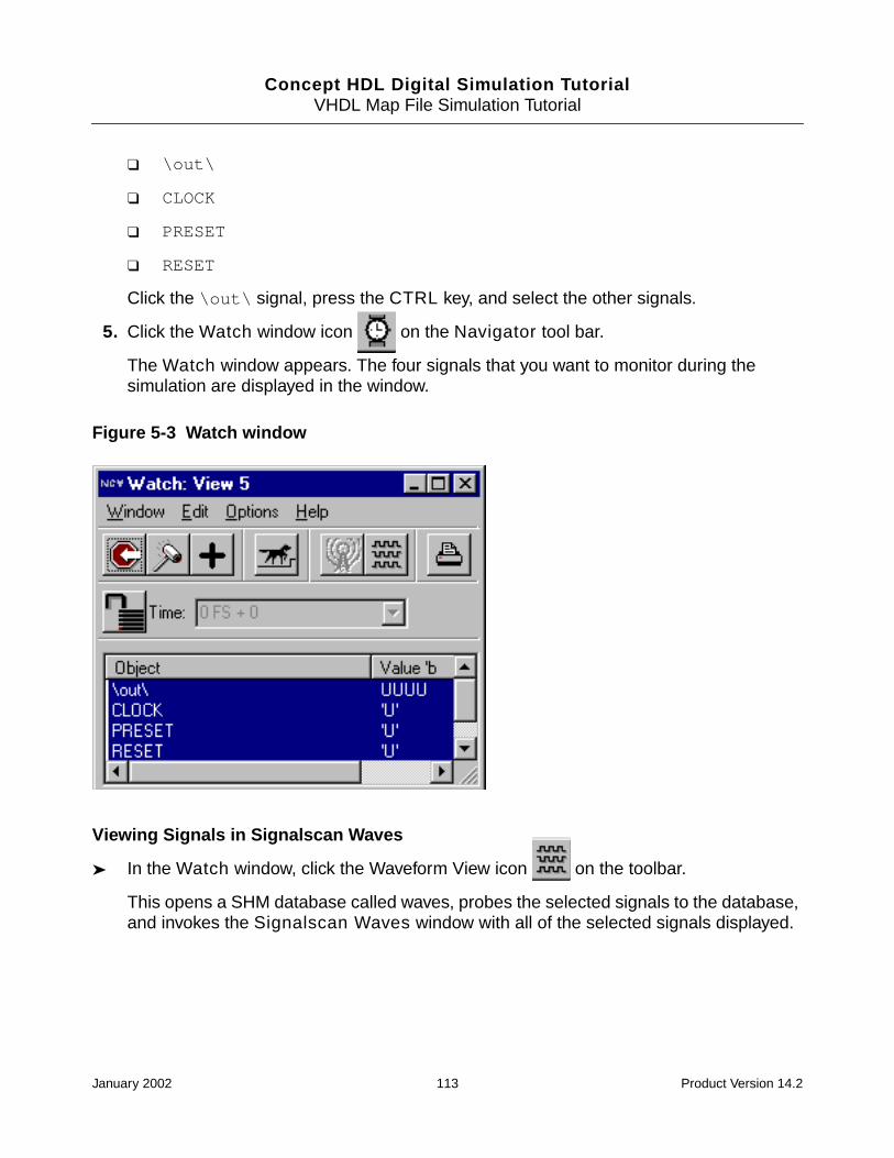
Concept HDL Digital Simulation TutorialVHDL Map File Simulation Tutorial
❑ \out\
❑ CLOCK
❑ PRESET
❑ RESET
Click the \out\ signal, press the CTRL key, and select the other signals.
5. Click the Watch window icon on the Navigator tool bar.
The Watch window appears. The four signals that you want to monitor during thesimulation are displayed in the window.
Figure 5-3 Watch window
Viewing Signals in Signalscan Waves
➤ In the Watch window, click the Waveform View icon on the toolbar.
This opens a SHM database called waves, probes the selected signals to the database,and invokes the Signalscan Waves window with all of the selected signals displayed.
January 2002 113 Product Version 14.2

Concept HDL Digital Simulation TutorialVHDL Map File Simulation Tutorial
Figure 5-4 Signal Scan Waves window
Look at the SimControl window. Each Tcl command that you have executed using theSimVision windows is echoed in the simulator Input/Output region.
A scope command was executed whenever you changed the scope. The waveformdatabase was created with the database command, and the signals were added to thewaveform database with the probe command.
You are now ready to simulate the design.
Simulating the Design
This section describes the procedures for simulating the design and viewing the results. Italso gives an overview of the cross-probing of signals and component instances betweenConcept HDL and NC VHDL.
1. Switch to the SimControl window (see Figure 5-1 on page 109).
Notice that in the toolbar, Time displayed is 0. This indicates that NC VHDL is stoppedat time 0 for you to specify the stimulus.
January 2002 114 Product Version 14.2

Concept HDL Digital Simulation TutorialVHDL Map File Simulation Tutorial
2. Click the Run Simulation icon in the toolbar.
Notice how the simulation time updates in the SimControl window just under the toolbar. Also notice that the waveforms update dynamically in the Signalscan Waveswindow as the simulation runs.The Watch window is updated when the simulation iscomplete. The Watch window displays the value of the signals after the simulation.
Viewing the Waveforms in Signalscan Waves
Once the simulation is complete, the Signalscan Waves window displays the updatedwaveforms for the signals. At this point, the waveform viewer is zoomed in to the end of thesimulation.
1. Click the ZmOutXFull button on the tool bar.
2. Click the ZoomInX button to zoom in until you can view the transitions on the signals.
To zoom in on a time region:
1. Select a signal transition. This inserts one cursor.
2. Insert a second cursor by clicking the middle mouse button (in UNIX) and the right mousebutton in Windows NT.
January 2002 115 Product Version 14.2

Concept HDL Digital Simulation TutorialVHDL Map File Simulation Tutorial
3. Click the ZoomInX button to zoom in between the cursors.
Cross-probing between Concept HDL and NC VHDL
Cross-probing is an effective way of debugging a design. Through cross-probing you canselect a component or net in Concept HDL and view its value in NC VHDL using SimVisionor Signalscan Waves.This section describes the procedures for cross-probing signals andcomponent instances between Concept HDL and NC VHDL.
Cross-probing Signals
1. In Concept HDL, click on the PRESET signal at the top of the schematic.
The signal is highlighted in the source browser of the SimControl window (seeFigure 5-1 on page 109). Use the scroll bar in the source browser to view the highlightedsignal.
2. In the SimControl window, click the Waveform View icon on the toolbar. Thewaveform for the signal is displayed in the SignalScan window.
Cross-probing Component Instances
January 2002 116 Product Version 14.2

Concept HDL Digital Simulation TutorialVHDL Map File Simulation Tutorial
1. In Concept HDL, click on the 74AC74 component instance on the right of the schematic.
The component instance is highlighted in the source browser of the SimControl window.Use the scroll bar in the source browser to view the highlighted component instance.
2. In the SimControl window, click the Waveform View icon on the toolbar. Thewaveform for all the signals in the scope of the component instance are opened inSignalScan window.
Similarly, you can probe other components used in the schematic design. Select File >Exit to close the SimControl window.
January 2002 117 Product Version 14.2

Concept HDL Digital Simulation TutorialVHDL Map File Simulation Tutorial
January 2002 118 Product Version 14.2

Concept HDL Digital Simulation Tutorial
6SDF Annotation
This tutorial demonstrates the steps for backannotating Allegro-generated Standard DelayFormat (SDF) files using the Verilog-XL simulation interface dialog box. Backannotation is theprocess of updating schematic design simulation information, such as component locationand electrical characteristics of the parts used in the schematic. Backannotation involvesusing implementation-specific information to improve the design, and therefore, forcalculating delays accurately it is important that you first complete the layout or the routing forthe design.
This tutorial covers the steps for backannotating the information contained in anAllegro-generated SDF file to a schematic designed in Concept HDL.
To backannotate SDF files, you need to complete the following sequence of tasks:
■ Simulating the Design
■ Packaging the Design
■ Creating the Board
■ Generating the SDF File
■ Backannotating Net Delay
This tutorial will take you through these tasks using a design example. The simulator used isVerilog-XL. Figure 6-1 on page 120 shows the Verilog-XL simulation flow with wire delays.
This tutorial assumes familiarity with Allegro and the digital simulation flow withoutbackannotating delay information from Allegro. This tutorial will not take you through the stepsfor performing digital simulation.
January 2002 119 Product Version 14.2
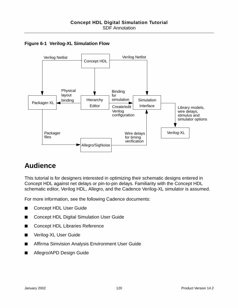
Concept HDL Digital Simulation TutorialSDF Annotation
Figure 6-1 Verilog-XL Simulation Flow
Audience
This tutorial is for designers interested in optimizing their schematic designs entered inConcept HDL against net delays or pin-to-pin delays. Familiarity with the Concept HDLschematic editor, Verilog HDL, Allegro, and the Cadence Verilog-XL simulator is assumed.
For more information, see the following Cadence documents:
■ Concept HDL User Guide
■ Concept HDL Digital Simulation User Guide
■ Concept HDL Libraries Reference
■ Verilog-XL User Guide
■ Affirma Simvision Analysis Environment User Guide
■ Allegro/APD Design Guide
Concept HDL
Packager-XLSimulationHierarchy
Allegro/SigNoise
Editor Interface
Physicallayoutbinding
Bindingforsimulation
Verilog Netlist Verilog Netlist
Wire delaysfor timingverification
Packagerfiles
Verilog-XL
Library models,wire delays,stimulus andsimulator options
Create/editVerilogconfiguration
January 2002 120 Product Version 14.2

Concept HDL Digital Simulation TutorialSDF Annotation
How to Use this Tutorial
This tutorial uses a design example to walk you through the tasks involved in performingdigital simulation using SDF files. The schematic editor used is Concept HDL and thesimulator is the Cadence Verilog-XL simulator.
Before using the tutorial, you need to install the design example.
Installing the Design Example
For the complete SDF flow, you need the following tools:
■ Project Manager (for product settings)
■ Concept HDL (for designing/editing the design)
■ Packager-XL (for packaging the design)
■ Allegro (for designing the physical layout)
■ SPECCTRA (for auto routing)
All of the above tools are available in the PCB Design Expert suite. You might want to use thissuite for going through the complete flow.
This tutorial uses a design, backann. To create a local copy of the design example databaseused in this tutorial, use the following procedure.
On the UNIX Platform
1. Open a UNIX shell window.
2. Change to the directory in which you want to install the design example database.
3. Copy the sdf_anno_ex.t.Z file located at <your_install_dir>/share/fet/examples/lwbhdl/ to the current directory.
The your_install_dir variable specifies the directory where you have installed theCadence PCB Design software. You can find the installation location by typingcds_root in a UNIX shell window.
4. At the command prompt, execute the following command:
zcat sdf_anno_ex.t.Z | tar xvof -
This command creates a directory called sdf_anno_ex in the current directory.
January 2002 121 Product Version 14.2

Concept HDL Digital Simulation TutorialSDF Annotation
5. Change the directory to the design example project directory, using the followingcommand.
cd sdf_anno_ex
6. Set the following environment variables:
❑ CONCEPT_INST_DIR to point to the directory where you have installed the CadencePCB Design software. For example, if you have installed the PSD software at /cdsinst/psd142, use the following command:
setenv CONCEPT_INST_DIR /cdsinst/psd142
❑ LDV_INST_DIR to point to the directory where you have installed the Cadence LDVsoftware. For example, if you have installed the LDV software at /cdsinst/ldv3,use the following command:
setenv LDV_INST_DIR /cdsinst/ldv3
On the Windows NT Platform
1. Browse to the following directory:
your_install_dir\share\fet\examples\lwbhdl\
The your_install_dir variable specifies the directory where you have installed theCadence PCB Design software.
2. Unzip the sdf_anno_ex.zip file to the directory where you want to install the designexample database. A directory called sdf_anno_ex is created.
3. Set the following environment variables:
❑ CONCEPT_INST_DIR to point to the directory where you have installed the CadencePCB Design software. For example, if you have installed the PSD software atC:\PSD142, set the CONCEPT_INST_DIR environment variable to point to thatlocation.
❑ LDV_INST_DIR to point to the directory where you have installed the Cadence LDVsoftware. For example, if you have installed the LDV software at C:\LDV3, set theLDV_INST_DIR environment variable to point to that location.
Simulating the Design
The schematic used in this design example is shown in Figure 6-2 on page 123.
This section gives you an overview of the steps for simulating the schematic in Verilog-XLsimulator.
January 2002 122 Product Version 14.2

Concept HDL Digital Simulation TutorialSDF Annotation
Figure 6-2 Schematic Design in Concept HDL
To simulate the design, complete the following tasks:
1. Generate the testbench. To generate the testbench, first generate the simulation netlistsim_sch_1 and then generate the testbench using stim.v as the stimulus file andtimescale as 1ns/100ps.
Contents of the stim.v file are shown below:
initial
begin
a = 0;
#20 a = 1;
#20 a = 0;
#20 a = 1;
#20 a = 0;
end
2. Specify the Design Instance as top.
3. Include the testbench and simulate the design.
4. View the output in the Signalscan window. The output waveform is shown in Figure 6-3on page 124.
January 2002 123 Product Version 14.2

Concept HDL Digital Simulation TutorialSDF Annotation
Figure 6-3 Output Waveforms
In the above figure signals f, g, and h are the output signals and a is the input signal (seeFigure 6-2 on page 123). Cursor1 indicates the time when the input signal changes the statefrom 1 to 0. Cursor2 indicates the time when all the output signals have changed their statefrom 0 to 1.
Note: The slight delay between Cursor1 and Cursor2 shown in Figure 6-3 on page 124indicates the component delay. This delay is maximum for the signal F because thenumber of components between signal A and signal F is the maximum. The delaybetween signal A and signal G is the same as the delay between signal A and signal Hbecause the number of components between the two signals is the same.
Note: To see the detailed steps for performing digital simulation using Verilog-XL, see DigitalSimulation Overview on page 12.
Packaging the Design
After simulating the design, you need to package the design. For packaging your schematicdesigns, you use a tool called Packager-XL.
Steps
1. To start Packager-XL, click Design Sync in Project Manager.
2. Select Export Physical.
The Export Physical dialog box appears.
January 2002 124 Product Version 14.2

Concept HDL Digital Simulation TutorialSDF Annotation
Figure 6-4 The Export Physical Dialog Box
3. To package the design, select the Package Design check box.
4. Select one of the packaging options. Select the Repackage option if you are packagingthe design for the first time.
5. Click OK.
The files that are created after you package your design are saved in the ./worklib/top/packaged view.
Note: To know more above packaging your designs, see the Cadence documentDesign Synchronization and Packaging User Guide.
Creating the Board
After packaging the design, the next step is to place the components on the board. For thecurrent design example, we will create an Allegro board, placed.brd.
January 2002 125 Product Version 14.2

Concept HDL Digital Simulation TutorialSDF Annotation
Steps
1. To start Allegro, click Layout in Project Manager.
2. To import the logical design in Allegro, choose File > Import > Logic.
The Import Logic dialog box appears with the Logic type tab selected.
3. Select the HDL-Concept option.
The Import from text box shows the location of the packaged view.
4. Click Import.
After the design is imported to Allegro, a new view, physical, is created.
Note: If you select the Update Allegro Board (Netrev) check box in theExport Physical dialog box, you need not perform the import logic step. Selecting theUpdate Allegro Board (Netrev) check box converts the files containing the packaginginformation to Allegro understandable format and also creates the physical view.
5. Next, you need to place the design components. In Allegro, choose Place > Manually.
The Placement dialog box appears with the Placement List tab selected.
January 2002 126 Product Version 14.2

Concept HDL Digital Simulation TutorialSDF Annotation
6. To place the components, select the Components by refdes check box and click on theboard to place the components.
7. Click OK.
8. Save the board design as placed.brd.
9. Choose Route > SPECTRA > Route Automatic to route the design.
10. Finally, save the placed.brd file.
Generating the SDF File
Next, you will generate the SDF file with the net delays. The command used for generatingnet delays is
a2sdf -s placed.brd
where
The delay file placed.sdf is generated. This file is located in thebackann_lib:top:physical view. The contents of placed.sdf file are shown below:
(DELAYFILE
(DESIGN "allegro")
(DATE "")
(VENDOR "Cadence")
(PROGRAM "AllegroSNA")
(VERSION "1.1")
(DIVIDER .)
(VOLTAGE )
(PROCESS "" )
(TEMPERATURE )
(TIMESCALE 1ns)
(CELL
(CELLTYPE "")
(INSTANCE )
(DELAY
-s the option to generate a wiredelay file
placed.brd the .brd file from which thewire delay data is to beextracted
January 2002 127 Product Version 14.2

Concept HDL Digital Simulation TutorialSDF Annotation
(ABSOLUTE
(INTERCONNECTˆbackann_lib˙top‹sch_1›\:page1_i3ˆbackann_lib˙hc04‹chips›\:\\y\*\\‹0›ˆbackann_lib˙top‹sch_1›\:page1_i7ˆbackann_lib˙hc04‹chips›\:a‹0›(:0.915:2.418) (:0.634:1.634))
(INTERCONNECTˆbackann_lib˙top‹sch_1›\:page1_i2ˆbackann_lib˙hc04‹chips›\:\\y\*\\‹0›ˆbackann_lib˙top‹sch_1›\:page1_i3ˆbackann_lib˙hc04‹chips›\:a‹0›(:1.174:2.647) (:0.893:1.854))
(INTERCONNECTˆbackann_lib˙top‹sch_1›\:page1_i1ˆbackann_lib˙hc04‹chips›\:\\y\*\\‹0›ˆbackann_lib˙top‹sch_1›\:page1_i2ˆbackann_lib˙hc04‹chips›\:a‹0›(:1.079:3.815) (:0.733:2.142))
(INTERCONNECTˆbackann_lib˙top‹sch_1›\:page1_i1ˆbackann_lib˙hc04‹chips›\:\\y\*\\‹0›ˆbackann_lib˙top‹sch_1›\:page1_i4ˆbackann_lib˙hc04‹chips›\:a‹0›(:1.226:3.678) (:0.890:2.265))
(INTERCONNECTˆbackann_lib˙top‹sch_1›\:page1_i1ˆbackann_lib˙hc04‹chips›\:\\y\*\\‹0›ˆbackann_lib˙top‹sch_1›\:page1_i5ˆbackann_lib˙hc04‹chips›\:a‹0›(:1.602:3.261) (:1.320:2.403))
(INTERCONNECTˆbackann_lib˙top‹sch_1›\:page1_i6ˆbackann_lib˙hc04‹chips›\:\\y\*\\‹0›ˆbackann_lib˙top‹sch_1›\:page1_i1ˆbackann_lib˙hc04‹chips›\:a‹0›(:0.913:2.439) (:0.620:1.663))
...
...
)
Note: The lines containing the delay information are in bold typeface.
The file, placed.sdf, contains delay information for each net in the schematic design. Thedelay information is listed under the keyword DELAY. The ABSOLUTE keyword specifies thedelay values that replace the existing delay values in the design. The INTERCONNECTkeyword lists the net location and the delay. The format used for the INTERCONNECT keywordis
(INTERCONNECT port_path1 port_path2 delay_list)
January 2002 128 Product Version 14.2

Concept HDL Digital Simulation TutorialSDF Annotation
where
For example, consider the following statement:
(INTERCONNECTˆbackann_lib˙top‹sch_1›\:page1_i3ˆbackann_lib˙hc04‹chips›\:\\y\*\\‹0›ˆbackann_lib˙top‹sch_1›\:page1_i7ˆbackann_lib˙hc04‹chips›\:a‹0›(:0.915:2.418) (:0.634:1.634))
In the above statement
❑ port_path1 isbackann_lib˙top‹sch_1›\:page1_i3ˆbackann_lib˙hc04‹chips›\:\\y\*\\‹0›
❑ port_path2 isbackann_lib˙top‹sch_1›\:page1_i7ˆbackann_lib˙hc04‹chips›\:a‹0›
❑ delay_list is (:0.915:2.418) (:0.634:1.634)
In the above example, delay_list consists of two (minimum:typical:maximum)triplets, one for the rising edge of the signal and the other for the falling edge,respectively.
The example statement lists the delay from the net between the instance I3 of hco4 on Page1 of the backann_lib:top:sch_1 view and instance I7 of hco4 on Page 1 of thebackann_lib:top:sch_1 view. The statement also lists the pin names that are connectedwith the concerned net. In the above example, the net is connected to pin yo of instance I3and pin ao of instance I7.
Arguments... Description...
port_path1 Is the Output or the inout port, from where the signal entersthe net
port_path2 Is the input or the inout port, from where the signal leaves thenet
delay_list Specifies the interconnect delay between port_path1 andport_path2
January 2002 129 Product Version 14.2

Concept HDL Digital Simulation TutorialSDF Annotation
Note: To know the pin name in Concept HDL, place the cursor at the tip of the pin. The pinname appears as a tooltip, as shown below.
The first entry in the delay_list, (:0.915:2.418), gives the delay in-time or the time atwhich the signal was at the first pin, pin yo of I3. The second entry, (:0.634:1.634), givesdelay in the out-time or the time at which the signal reached the second pin, a0 of I7. Thedifference between these two values gives the net delay.
Backannotating Net Delay
After the delay information is generated by Allegro, the next step is to simulate the designusing the delay information. To do this, complete the following steps:
1. In Concept HDL, choose Tools > Simulate.
The Verilog-XL simulation interface dialog box appears.
2. Click Setup.
3. Select the Allegro SDF tab.
4. Select the Perform SDF Annotation check box.
5. In the Allegro SDF File text box, specify the location of the Allegro-generated SDF file.By default, the file is located in the physical view. For the current design example, youneed to specify the location of the placed.sdf file.
6. Specify testfixture.top as Scope.
Note: Usually, the scope is textfixture.<design_instance>. For the currentdesign example, the design instance is top.
January 2002 130 Product Version 14.2

Concept HDL Digital Simulation TutorialSDF Annotation
7. To annotate maximum delay, specify Delay Type as Maximum and Scale Type asFrom Maximum.
To know more about the options in the Allegro SDF tabbed page, see Appendix A,“Dialog Box Reference”, of Concept HDL Digital Simulation User Guide.
8. For the current design example, specify Scale Factors as 5.0:5.0:5.0.
9. If you want the SDF annotation log file to be generated, select the Generate SDF BackAnnotation Log check box.
The Allegro SDF tabbed page with all the selections is shown below:
10. Click OK to save the settings.
11. Click Run to simulate the design using SDF.
January 2002 131 Product Version 14.2

Concept HDL Digital Simulation TutorialSDF Annotation
The Simulation progress status box appears.
When you click Run, following tasks are performed.
❑ The Allegro-generated SDF file is converted to a format that is understood by verilogsimulators. This conversion is required because the SDF file generated by Allegrois in a format that is not understood by Verilog-XL. By default, the SDF file in theverilog format is saved in the cfg_verilog/sim1 view by the name delay.sdf.The delay.sdf file is used for backannotation. A part of the delay.sdf file isshown below:
(DELAYFILE
(SDFVERSION "1.0")
(DESIGN "allegro")
(DATE "")
(VENDOR "Cadence")
(PROGRAM "AllegroSNA")
January 2002 132 Product Version 14.2

Concept HDL Digital Simulation TutorialSDF Annotation
(VERSION "1.1")
(DIVIDER .)
(PROCESS "")
(TIMESCALE 1 ns)
(CELL
(CELLTYPE "")
(INSTANCE )
(DELAY
(ABSOLUTE
(INTERCONNECT top.page1_i3._6Y top.page1_i7._6A (:0.915:2.418)(:0.634:1.634))
(INTERCONNECT top.page1_i2._6Y top.page1_i3._6A (:1.174:2.647)(:0.893:1.854))
(INTERCONNECT top.page1_i1._6Y top.page1_i2._6A (:1.079:3.815)(:0.733:2.142))
(INTERCONNECT top.page1_i1._6Y top.page1_i4._6A (:1.226:3.678)(:0.890:2.265))
(INTERCONNECT top.page1_i1._6Y top.page1_i5._6A (:1.602:3.261)(:1.320:2.403))
(INTERCONNECT top.page1_i6._6Y top.page1_i1._6A (:0.913:2.439)(:0.620:1.663)))))
)
❑ A verilog file, sdf.v, located at cfg_verilog/sim1, is also generated. This filecontains all the options you specified in the Allegro SDF tabbed page. This file alsospecifies the location of the delay.sdf file.
❑ The sdf.v file is passed to the Cadence Verilog-XL simulator. The contents of thesdf.v file are shown below:
module sdf_annotate();
initial
$sdf_annotate("./worklib/top/cfg_verilog/sim1/delay.sdf",testfixture.test,,"./worklib/top/cfg_verilog/sim1/sdf.log","TYPICAL","5.0:5.0:5.0","FROM_TYPICAL");
endmodule
After the SDF files are generated, Cadence Verilog-XL starts.
To view the output waveforms, complete the following steps:
January 2002 133 Product Version 14.2

Concept HDL Digital Simulation TutorialSDF Annotation
12. In the Verilog-XL simulator, choose Select > Signals.
13. Click the right mouse button and select Wave Trace.
Signalscan waveform window appears.
14. In the Verilog-XL simulator, click Run to run the simulation.
15. In the Signalscan window click ZmOutXFull.
Figure 6-5 on page 134 displays the output waveforms after backannotating the net delay.
Figure 6-5 Output Waveforms after SDF Annotation
As per the Figure 6-5 on page 134, there is a maximum delay of 17,680 ps. This delay is thedifference between the time when the output signal F changes its state from 0 to 1 (57,850ps) and the time when the input signal A changes its state from 1 to 0 (40170 ps). To get theactual delay, you need to divide the delay by the scaling factor. For the current designexample, you specified the scaling factor as 5 in the Allegro SDF tab. Therefore, for theabove example, the actual delay is 3536 ps.
The pin-to-pin or net delay is influenced both by the number and by the length of the nets.Signalscan Waveform shows the maximum delay for signal F and the minimum delay forsignal G. Even though the number of parts is the same, the delay for signal H is more than thedelay for signal G because of the length of the net.
By looking at the simulation results obtained after backannotating SDF files, schematicdesigners can take steps to optimize their design. For example, if the net delay does not meetthe timing constraint, schematic designers might decide to make changes to the original
January 2002 134 Product Version 14.2

Concept HDL Digital Simulation TutorialSDF Annotation
design. If the delay in the rising edge or the falling edge is not acceptable, the schematicdesigner might want to change the part itself.
Important
The actual delays that you get when you take the same design example through thecompleted SDF flow on your machines might be different from the delays shown inthe tutorial. This is because delays are influenced to a large extent by the placementof components on the Allegro board.
January 2002 135 Product Version 14.2

Concept HDL Digital Simulation TutorialSDF Annotation
January 2002 136 Product Version 14.2