Computer Structure Part I : combinational modulesmedinamo/Computer_Structure/class_notes.pdf ·...
137
Computer Structure Part I : combinational modules by Guy Even op-gate op-gate op-gate op-gate op-gate op-gate op-gate y[0] x[0] x[1] x[2] x[3] x[n - 4] x[n - 3] x[n - 2] x[n - 1] y[1] y[2] y[3] y[n - 4] y[n - 3] y[n - 2] y[n - 1] x 0 [n/2 - 1] x 0 [n/2 - 2] x 0 [1] x 0 [0] y 0 [n/2 - 1] y 0 [n/2 - 2] y 0 [1] y 0 [0] ppc–op(n/2) Lecture Notes : Spring 2007 School of Electrical Engineering, Tel-Aviv University
-
Upload
nguyenliem -
Category
Documents
-
view
215 -
download
0
Transcript of Computer Structure Part I : combinational modulesmedinamo/Computer_Structure/class_notes.pdf ·...

Computer StructurePart I : combinational modules
by
Guy Even
op-gateop-gateop-gate
op-gateop-gateop-gateop-gate
y[0]
x[0]x[1]x[2]x[3]x[n− 4]x[n − 3]x[n− 2]x[n − 1]
y[1]y[2]y[3]y[n− 4]y[n − 3]y[n− 2]y[n− 1]
x′[n/2 − 1] x′[n/2 − 2] x′[1] x′[0]
y′[n/2 − 1] y′[n/2 − 2] y′[1] y′[0]ppc–op(n/2)
Lecture Notes : Spring 2007School of Electrical Engineering, Tel-Aviv University

Contents
1 The digital abstraction 1
1.1 Transistors . . . . . . . . . . . . . . . . . . . . . . . . . . . . . . . . . . . 2
1.2 From analog signals to digital signals . . . . . . . . . . . . . . . . . . . . 3
1.3 Transfer functions of gates . . . . . . . . . . . . . . . . . . . . . . . . . . 6
1.4 The bounded-noise model . . . . . . . . . . . . . . . . . . . . . . . . . . 8
1.5 The digital abstraction in presence of noise . . . . . . . . . . . . . . . . . 8
1.5.1 Input and output signals . . . . . . . . . . . . . . . . . . . . . . . 9
1.5.2 Redefining the digital interpretation of analog signals . . . . . . . 9
1.6 Stable signals . . . . . . . . . . . . . . . . . . . . . . . . . . . . . . . . . 11
1.7 Summary . . . . . . . . . . . . . . . . . . . . . . . . . . . . . . . . . . . 12
2 Foundations of combinational circuits 13
2.1 Boolean functions . . . . . . . . . . . . . . . . . . . . . . . . . . . . . . . 14
2.2 Combinational gates - an analog approach . . . . . . . . . . . . . . . . . 14
2.3 Back to the digital world . . . . . . . . . . . . . . . . . . . . . . . . . . . 16
2.4 Building blocks . . . . . . . . . . . . . . . . . . . . . . . . . . . . . . . . 18
2.5 Combinational circuits . . . . . . . . . . . . . . . . . . . . . . . . . . . . 21
2.6 Cost and propagation delay . . . . . . . . . . . . . . . . . . . . . . . . . 25
2.7 Syntax and semantics . . . . . . . . . . . . . . . . . . . . . . . . . . . . . 26
2.8 Summary . . . . . . . . . . . . . . . . . . . . . . . . . . . . . . . . . . . 27
3 Trees 29
3.1 Trees of associative Boolean gates . . . . . . . . . . . . . . . . . . . . . . 30
3.1.1 Associative Boolean functions . . . . . . . . . . . . . . . . . . . . 30
3.1.2 or-trees . . . . . . . . . . . . . . . . . . . . . . . . . . . . . . . . 31
3.1.3 Cost analysis . . . . . . . . . . . . . . . . . . . . . . . . . . . . . 33
3.1.4 Delay analysis . . . . . . . . . . . . . . . . . . . . . . . . . . . . . 34
3.2 Optimality of trees . . . . . . . . . . . . . . . . . . . . . . . . . . . . . . 36
3.2.1 Definitions . . . . . . . . . . . . . . . . . . . . . . . . . . . . . . . 36
3.2.2 Lower bounds . . . . . . . . . . . . . . . . . . . . . . . . . . . . . 37
3.3 Summary . . . . . . . . . . . . . . . . . . . . . . . . . . . . . . . . . . . 41
iii

iv CONTENTS
4 Decoders and Encoders 434.1 Notation . . . . . . . . . . . . . . . . . . . . . . . . . . . . . . . . . . . . 444.2 Values represented by binary strings . . . . . . . . . . . . . . . . . . . . 464.3 Decoders . . . . . . . . . . . . . . . . . . . . . . . . . . . . . . . . . . . . 47
4.3.1 Brute force design . . . . . . . . . . . . . . . . . . . . . . . . . . . 484.3.2 An optimal decoder design . . . . . . . . . . . . . . . . . . . . . . 484.3.3 Correctness . . . . . . . . . . . . . . . . . . . . . . . . . . . . . . 494.3.4 Cost and delay analysis . . . . . . . . . . . . . . . . . . . . . . . . 50
4.4 Encoders . . . . . . . . . . . . . . . . . . . . . . . . . . . . . . . . . . . . 514.4.1 Implementation . . . . . . . . . . . . . . . . . . . . . . . . . . . . 524.4.2 Cost and delay analysis . . . . . . . . . . . . . . . . . . . . . . . . 554.4.3 Yet another encoder . . . . . . . . . . . . . . . . . . . . . . . . . 56
4.5 Summary . . . . . . . . . . . . . . . . . . . . . . . . . . . . . . . . . . . 57
5 Selectors and Shifters 595.1 Multiplexers . . . . . . . . . . . . . . . . . . . . . . . . . . . . . . . . . . 60
5.1.1 Implementation . . . . . . . . . . . . . . . . . . . . . . . . . . . . 605.2 Cyclic Shifters . . . . . . . . . . . . . . . . . . . . . . . . . . . . . . . . . 62
5.2.1 Implementation . . . . . . . . . . . . . . . . . . . . . . . . . . . . 635.3 Logical Shifters . . . . . . . . . . . . . . . . . . . . . . . . . . . . . . . . 66
5.3.1 Implementation . . . . . . . . . . . . . . . . . . . . . . . . . . . . 675.4 Arithmetic Shifters . . . . . . . . . . . . . . . . . . . . . . . . . . . . . . 685.5 Summary . . . . . . . . . . . . . . . . . . . . . . . . . . . . . . . . . . . 69
6 Priority encoders 716.1 Big Endian vs. Little Endian . . . . . . . . . . . . . . . . . . . . . . . . 726.2 Priority Encoders . . . . . . . . . . . . . . . . . . . . . . . . . . . . . . . 73
6.2.1 Implementation of u-penc(n) . . . . . . . . . . . . . . . . . . . . 756.2.2 Implementation of b-penc . . . . . . . . . . . . . . . . . . . . . . 77
6.3 Summary . . . . . . . . . . . . . . . . . . . . . . . . . . . . . . . . . . . 80
7 Half-Decoders 817.1 Specification . . . . . . . . . . . . . . . . . . . . . . . . . . . . . . . . . . 827.2 Preliminaries . . . . . . . . . . . . . . . . . . . . . . . . . . . . . . . . . 827.3 Implementation . . . . . . . . . . . . . . . . . . . . . . . . . . . . . . . . 847.4 Correctness . . . . . . . . . . . . . . . . . . . . . . . . . . . . . . . . . . 847.5 Cost and delay analysis . . . . . . . . . . . . . . . . . . . . . . . . . . . . 867.6 Application . . . . . . . . . . . . . . . . . . . . . . . . . . . . . . . . . . 877.7 Summary . . . . . . . . . . . . . . . . . . . . . . . . . . . . . . . . . . . 87
8 Addition 898.1 Definition of a binary adder . . . . . . . . . . . . . . . . . . . . . . . . . 918.2 Ripple Carry Adder . . . . . . . . . . . . . . . . . . . . . . . . . . . . . . 91
8.2.1 Correctness proof . . . . . . . . . . . . . . . . . . . . . . . . . . . 92

CONTENTS v
8.2.2 Delay and cost analysis . . . . . . . . . . . . . . . . . . . . . . . . 938.3 Carry bits . . . . . . . . . . . . . . . . . . . . . . . . . . . . . . . . . . . 93
8.3.1 Redundant and non redundant representation . . . . . . . . . . . 948.3.2 Cone of adder outputs . . . . . . . . . . . . . . . . . . . . . . . . 958.3.3 Reductions between sum and carry bits . . . . . . . . . . . . . . . 95
8.4 Conditional Sum Adder . . . . . . . . . . . . . . . . . . . . . . . . . . . 958.4.1 Motivation . . . . . . . . . . . . . . . . . . . . . . . . . . . . . . . 968.4.2 Implementation . . . . . . . . . . . . . . . . . . . . . . . . . . . . 968.4.3 Delay and cost analysis . . . . . . . . . . . . . . . . . . . . . . . . 96
8.5 Compound Adder . . . . . . . . . . . . . . . . . . . . . . . . . . . . . . . 988.5.1 Implementation . . . . . . . . . . . . . . . . . . . . . . . . . . . . 998.5.2 Correctness . . . . . . . . . . . . . . . . . . . . . . . . . . . . . . 998.5.3 Delay and cost analysis . . . . . . . . . . . . . . . . . . . . . . . . 100
8.6 Summary . . . . . . . . . . . . . . . . . . . . . . . . . . . . . . . . . . . 101
9 Fast Addition 1039.1 Reduction: sum-bits 7−→ carry-bits . . . . . . . . . . . . . . . . . . . . . 1049.2 Computing the carry-bits . . . . . . . . . . . . . . . . . . . . . . . . . . . 104
9.2.1 Carry-Lookahead Adders . . . . . . . . . . . . . . . . . . . . . . . 1059.2.2 Reduction to prefix computation . . . . . . . . . . . . . . . . . . 108
9.3 Parallel prefix computation . . . . . . . . . . . . . . . . . . . . . . . . . . 1109.3.1 Implementation . . . . . . . . . . . . . . . . . . . . . . . . . . . . 1119.3.2 Correctness . . . . . . . . . . . . . . . . . . . . . . . . . . . . . . 1119.3.3 Delay and cost analysis . . . . . . . . . . . . . . . . . . . . . . . . 113
9.4 Putting it all together . . . . . . . . . . . . . . . . . . . . . . . . . . . . 1149.5 Summary . . . . . . . . . . . . . . . . . . . . . . . . . . . . . . . . . . . 114
10 Signed Addition 11710.1 Representation of negative integers . . . . . . . . . . . . . . . . . . . . . 11810.2 Negation in two’s complement representation . . . . . . . . . . . . . . . . 11810.3 Properties of two’s complement representation . . . . . . . . . . . . . . . 12110.4 Reduction: two’s complement addition to binary addition . . . . . . . . . 122
10.4.1 Detecting overflow . . . . . . . . . . . . . . . . . . . . . . . . . . 12410.4.2 Determining the sign of the sum . . . . . . . . . . . . . . . . . . . 125
10.5 A two’s-complement adder . . . . . . . . . . . . . . . . . . . . . . . . . . 12610.6 A two’s complement adder/subtracter . . . . . . . . . . . . . . . . . . . . 12710.7 Additional questions . . . . . . . . . . . . . . . . . . . . . . . . . . . . . 12910.8 Summary . . . . . . . . . . . . . . . . . . . . . . . . . . . . . . . . . . . 131

vi CONTENTS

Chapter 1
The digital abstraction
Contents
1.1 Transistors . . . . . . . . . . . . . . . . . . . . . . . . . . . . . 2
1.2 From analog signals to digital signals . . . . . . . . . . . . . 3
1.3 Transfer functions of gates . . . . . . . . . . . . . . . . . . . . 6
1.4 The bounded-noise model . . . . . . . . . . . . . . . . . . . . 8
1.5 The digital abstraction in presence of noise . . . . . . . . . . 8
1.5.1 Input and output signals . . . . . . . . . . . . . . . . . . . . . . 9
1.5.2 Redefining the digital interpretation of analog signals . . . . . 9
1.6 Stable signals . . . . . . . . . . . . . . . . . . . . . . . . . . . . 11
1.7 Summary . . . . . . . . . . . . . . . . . . . . . . . . . . . . . . 12
Preliminary Questions:
1. Can you justify or explain the saying that “computers use only zeros and ones”?
2. Can you explain the following anomaly? The design of an adder is a simple task.However, the design and analysis of a single electronic device (e.g., a single gate) isa complex task.
1
2 CHAPTER 1. THE DIGITAL ABSTRACTION
The term a digital circuit refers to a device that works in a binary world. In the binaryworld, the only values are zeros and ones. In other words, the inputs of a digital circuitare zeros and ones, and the outputs of a digital circuit are zeros and ones. Digital circuitsare usually implemented by electronic devices and operate in the real world. In the realworld, there are no zeros and ones; instead, what matters is the voltages of inputs andoutputs. Since voltages refer to energy, they are continuous1. So we have a gap betweenthe continuous real world and the two-valued binary world. One should not regard thisgap as an absurd. Digital circuits are only an abstraction of electronic devices. In thischapter we explain this abstraction, called the digital abstraction.
In the digital abstraction one interprets voltage values as binary values. The advan-tages of the digital model cannot be overstated; this model enables one to focus on thedigital behavior of a circuit, to ignore analog and transient phenomena, and to easilybuild larger more complex circuits out of small circuits. The digital model together witha simple set of rules, called design rules, enable logic designers to design complex digitalcircuits consisting of millions of gates.
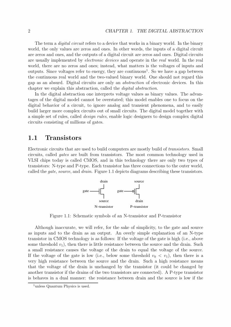
1.1 Transistors
Electronic circuits that are used to build computers are mostly build of transistors. Smallcircuits, called gates are built from transistors. The most common technology used inVLSI chips today is called CMOS, and in this technology there are only two types oftransistors: N-type and P-type. Each transistor has three connections to the outer world,called the gate, source, and drain. Figure 1.1 depicts diagrams describing these transistors.
gate gate
N−transistor
drain
drainsourceP−transistor
source
Figure 1.1: Schematic symbols of an N-transistor and P-transistor
Although inaccurate, we will refer, for the sake of simplicity, to the gate and sourceas inputs and to the drain as an output. An overly simple explanation of an N-typetransistor in CMOS technology is as follows: If the voltage of the gate is high (i.e., abovesome threshold v1), then there is little resistance between the source and the drain. Sucha small resistance causes the voltage of the drain to equal the voltage of the source.If the voltage of the gate is low (i.e., below some threshold v0 < v1), then there is avery high resistance between the source and the drain. Such a high resistance meansthat the voltage of the drain is unchanged by the transistor (it could be changed byanother transistor if the drains of the two transistors are connected). A P-type transistoris behaves in a dual manner: the resistance between drain and the source is low if the
1unless Quantum Physics is used.

1.2. FROM ANALOG SIGNALS TO DIGITAL SIGNALS 3
gate voltage is below v0. If the voltage of the gate is above v1, then the source-to-drainresistance is very high.
Note that this description of transistor behavior implies immediately that transistorsare highly non-linear. (Recall that a linear function f(x) satisfies f(a · x) = a · f(x).) Intransistors, changes of 10% in input values above the threshold v1 have a small effect onthe output while changes of 10% in input values between v0 and v1 have a large effecton the output. In particular, this means that transistors do not follow Ohm’s Law (i.e.,V = I ·R).
Example 1.1 (A CMOS inverter) Figure 1.2 depicts a CMOS inverter. If the inputvoltage is above v1, then the source-to-drain resistance in the P-transistor is very highand the source-to-drain resistance in the N-transistor is very low. Since the source of theN-transistor is connected to low voltage (i.e., ground), the output of the inverter is low.
If the input voltage is below v0, then the source-to-drain resistance in the N-transistoris very high and the source-to-drain resistance in the P-transistor is very low. Since thesource of the P-transistor is connected to high voltage, the output of the inverter is high.
We conclude that the voltage of the output is low when the input is high, and vice-versa, and the device is indeed an inverter.
OUTIN
0 volts
5 volts
N−transistor
P−transistor
Figure 1.2: A CMOS inverter
The qualitative description in Example 1.1 hopefully conveys some intuition abouthow gates are built from transistors. A quantitative analysis of such an inverter requiresprecise modeling of the functionality of the transistors in order to derive the input-output voltage relation. One usually performs such an analysis by computer programs(e.g. SPICE). Quantitative analysis is relatively complex and inadequate for designinglarge systems like computers. (This would be like having to deal with the chemistry ofink when using a pen.)
1.2 From analog signals to digital signals
An analog signal is a real function f : R → R that describes the voltage of a givenpoint in a circuit as a function of the time. We ignore the resistance and capacities ofwires. Moreover, we assume that signals propagate through wires immediately2. Under
2This is a reasonable assumption if wires are short.

4 CHAPTER 1. THE DIGITAL ABSTRACTION
these assumptions, it follows that, in every moment, the voltages measured along differentpoints of a wire are identical. Since a signal describes the voltage (i.e., derivative of energyas a function of electric charge), we also assume that a signal is a continuous function.
A digital signal is a function g : R→ 0, 1, non-logical. The value of a digital signaldescribes the logical value carried along a wire as a function of time. To be precise thereare two logical values: zero and one. The non-logical value simply means that that thesignal is neither zero or one.
How does one interpret an analog signal as a digital signal? The simplest interpreta-tion is to set a threshold V ′. Given an analog signal f(t), the digital signal dig(f(t)) canbe defined as follows.
dig(f(t))4
=
0 if f(t) < V ′
1 if f(t) > V ′(1.1)
According to this definition, a digital interpretation of an analog signal is always 0 or 1,and the digital interpretation is never non-logical.
There are several problems with the definition in Equation 1.1. One problem with thisdefinition is that all the components should comply with exactly the same threshold V ′.In reality, devices are not completely identical; the actual thresholds of different devicesvary according to a tolerance specified by the manufacturer. This means that instead ofa fixed threshold, we should consider a range of thresholds.
Another problem with the definition in Equation 1.1 is caused by perturbations off(t) around the threshold t. Such perturbations can be caused by noise or oscillationsof f(t) before it stabilizes. We will elaborate more on noise later, and now explain whyoscillations can occur. Consider a spring connected to the ceiling with a weight w hangingfrom it. We expect the spring to reach a length ` that is proportional to the weight w.Assume that all we wish to know is whether the length ` is greater than a threshold `t.Sounds simple! But what if ` is rather close to `t? In practice, the length only tends tothe length ` as time progresses; the actual length of the spring oscillates around ` witha diminishing amplitude. Hence, the length of the spring fluctuates below and above `t
many times before we can decide. This effect may force us to wait for a long time beforewe can decide if ` < `t. If we return to the definition of dig(f(t)), it may well happenthat f(t) oscillates around the threshold V ′. This renders the digital interpretation usedin Eq. 1.1 useless.
Returning to the example of weighing weights, assume that we have two types ofobjects: light and heavy. The weight of a light (resp., heavy) object is at most (resp., atleast) w0 (resp., w1). The bigger the gap w1 − w0, the easier it becomes to determine ifan object is light or heavy (especially in the presence of noise or oscillations).
Now we have two reasons to introduce two threshold values instead of one, namely,different threshold values for different devices and the desire to have a gap betweenvalues interpreted as logical zero and logical one. We denote these thresholds by Vlowand Vhigh, and require that Vlow < Vhigh. An interpretation of an analog signal is
depicted in Figure 1.3. Consider an analog signal f(t). The digital signal dig(f(t)) is

1.2. FROM ANALOG SIGNALS TO DIGITAL SIGNALS 5
defined as follows.
dig(f(t))4
=
0 if f(t) < Vlow1 if f(t) > Vhighnon-logical otherwise.
(1.2)
Vhigh
logical zero
f(t)
Vlow
logical one
t
Figure 1.3: A digital interpretation of an analog signal in the zero-noise model.
We often refer to the logical value of an analog signal f . This is simply a shorthandway of referring to the value of the digital signal dig(f).
It is important to note that fluctuations of f(t) are still possible around the thresholdvalues. However, if the two thresholds are sufficiently far away from each other, fluctua-tions of f do not cause fluctuations of dig(f(t)) between 0 and 1. Instead, we will have atworst fluctuations of dig(f(t)) between a non-logical value and a logical value (i.e., 0 or1). A fluctuation between a logical value and a non-logical value is much more favorablethan a fluctuation between 0 and 1. The reason is that a non-logical value is an indicationthat the circuit is still in a transient state and a “decision” has not been reached yet.
Assume that we design an inverter so that its output tends to a voltage that is boundedaway from the thresholds Vlow and Vhigh. Let us return to the example of the spring
with weight w hanging from it. Additional fluctuations in the length of the spring mightbe caused by wind. This means that we need to consider additional effects so that ourmodel will be useful. In the case of the digital abstraction, we need to take noise intoaccount. Before we consider the effect of noise, we formulate the static functionality of agate, namely, the values of its output as a function of its stable inputs.
Question 1.1 Try to define an inverter in terms of the voltage of the output as a functionof the voltage of the input.

6 CHAPTER 1. THE DIGITAL ABSTRACTION
1.3 Transfer functions of gates
The voltage at an output of a gate depends on the voltages of the inputs of the gate.This dependence is called the transfer function (or the voltage-transfer characteristic -VTC). Consider, for example an inverter with an input x and an output y. To makethings complicated, the value of the signal y(t) at time t is not only a function of thesignal x at time t since y(t) depends on the history. Namely, y(t0) is a function of x(t)over the interval (−∞, t0].
Partial differential equations are used to model gates, and the solution of these equa-tions is unfortunately a rather complicated task. A good approximation of transfer func-tions is obtain by solving differential equations, still a complicated task that can becomputed quickly only for a few transistors. So how are chips that contain millions ofchips designed if the models are too complex to be solved?
The way this very intricate problem is handled is by restricting designs. In particular,only a small set of building blocks is used. The building blocks are analyzed intensively,their properties are summarized, and designers rely on these properties for their designs.
One of the most important steps in characterizing the behavior of a gate is computingits static transfer function. Returning to the example of the inverter, a “proper” inverterhas a unique output value for each input value. Namely, if the input x(t) is stable for asufficiently long period of time and equals x0, then the output y(t) stabilizes on a valuey0 that is a function of x0.
Before we define what a static transfer function is, we point out that there are devicesthat do not have static transfer functions. We need to distinguish between two cases:(a) Stability is not reached: this case occurs, for example, with devices called oscillators.Note that oscillating devices must consume energy even when the input is stable. Wepoint out that in CMOS technology it is easy to design circuits that do not consumeenergy if the input is logical, so such oscillations are avoided. (b) Stability is reached:in this case, if there is more than one stable output value, it means that the devicehas more than one equilibrium point. Such a device can be used to store informationabout the “history”. It is important to note that devices with multiple equilibriums arevery useful as storage devices (i.e., they can “remember” a small amount of information).Nevertheless, devices with multiple equilibriums are not “good” candidates for gates, andit is easy to avoid such devices in CMOS technology.
Example 1.2 (A device with many equillibriums) Consider a pot that is initiallyfilled with water. At time t, the pot is held in angle x(t). A zero angle means that the potis held upright. An angle of 180 means that the pot is upside down. Now, we are toldthat x(t) = 0 for t ≥ 100. Can we say how much water is contained in the pot at timet = 200? The answer, of course, depends on the history during the interval t ∈ [0, 100),namely, whether the pot was tilted.
We formalize the definition of a static transfer function of a gate G with one input xand one output y in the following definition.

1.3. TRANSFER FUNCTIONS OF GATES 7
Definition 1.1 Consider a device G with one input x and one output y. The device Gis a gate if its functionality is specified by a function f : R → R as follows: there existsa ∆ > 0, such that, for every x0 and every t0, if x(t) = x0 for every t ∈ [t0 −∆, t0], theny(t0) = f(x0).Such a function f(x) is called the static transfer function of G.
At this point we should point the following remarks:
1. Since circuits operate over a bounded range of voltages, static transfer functionsare usually only defined over bounded domains and ranges (say, [0, 5] volts).
2. To make the definition useful, one should allow perturbations of x(t) during theinterval [t0 − ∆, t0]. Static transfer functions model physical devices, and hence,are continuous. This implies the following definition: For every ε > 0, there exist aδ > 0 and a ∆ > 0, such that
∀t ∈ [t1, t2] : |x(t)− x0| ≤ δ ⇒ ∀t ∈ [t1 + ∆, t2] : |y(t)− f(x0)| ≤ ε.
3. Note that in the above definition ∆ does not depend on x0 (although it may dependon ε). Typically, we are interested on the values of ∆ only for logical values of x(t)(i.e., x(t) ≤ Vlow and x(t) ≥ Vhigh). Once the value of ε is fixed, this constant
∆ is called the propagation delay of the gate G and is one of the most importantcharacteristic of a gate.
Question 1.2 Extend Definition 1.1 to gates with n inputs and m outputs.
Finally, we can now define an inverter in the zero-noise model. Observe that accordingto this definition a device is an inverter if its static transfer function satisfies a certainproperty.
Definition 1.2 (inverter in zero-noise model) A gate G with a single input x and asingle output y is an inverter if its static transfer function f(z) satisfies the following thefollowing two conditions:
1. If z < Vlow, then f(z) > Vhigh.
2. If z > Vhigh, then f(z) < Vlow.
The implication of this definition is that if the logical value of the input x is zero (resp.,one) during an interval [t1, t2] of length at least ∆, then the logical value of the output yis one (resp., zero) during the interval [t1 + ∆, t2].
How should we define other gates such a nand-gates, xor-gates, etc.? As in thedefinition of an inverter, the definition of a nand-gate is simply a property of its statictransfer function.
Question 1.3 Define a nand-gate.
We are now ready to strengthen the digital abstraction so that it will be useful also inthe presence of bounded noise.

8 CHAPTER 1. THE DIGITAL ABSTRACTION
1.4 The bounded-noise model
Consider a wire from point A to point B. Let A(t) denote the analog signal measured atpoint A. Similarly, let B(t) denote the analog signal measured at point B. We would liketo assume that wires have zero resistance, zero capacitance, and that signals propagatethrough a wire with zero delay. This assumption means that the signals A(t) and B(t)should be equal at all times. Unfortunately, this is not the case; the main reason for thisdiscrepancy is noise.
There are many sources of noise. The main source of noise is heat that causes electronsto move randomly. These random movements do not cancel out perfectly, and randomcurrents are created. These random currents create perturbations in the voltage. Thedifference between the signals B(t) and A(t) is a noise signal.
Consider, for example, the setting of additive noise: A is an output of an inverter andB is an input of another inverter. We consider the signal A(t) to be a reference signal.The signal B(t) is the sum A(t) + nB(t), where nB(t) is the noise signal.
The bounded-noise model assumes that the noise signal along every wire has a boundedabsolute value. We will use a slightly simplified model in which there is a constant ε > 0such that the absolute value of all noise signals is bounded by ε. We refer to this model asthe uniformly bounded noise model. The justification for assuming that noise is boundedis probabilistic. Noise is a random variable whose distribution has a rapidly diminishingtail. This means that if the bound is sufficiently large, then the probability of the noiseexceeding this bound during the lifetime of a circuit is negligibly small.
1.5 The digital abstraction in presence of noise
Consider two inverters, where the output of one gate feeds the input of the second gate.Figure 1.4 depicts such a circuit that consists of two inverters.
Assume that the input x has a value that satisfies: (a) x > Vhigh, so the logical value
of x is one, and (b) y = Vlow− ε′, for a very small ε′ > 0. This might not be possible withevery inverter, but Definition 1.2 does not rule out such an inverter. (Consider a transferfunction with f(Vhigh) = Vlow, and x slightly higher than Vhigh.) Since the logical value
of y is zero, it follows that the second inverter, if not faulty, should output a value z thatis greater than Vhigh. In other words, we expect the logical value of z to be 1. At this
point we consider the effect of adding noise.
Let us denote the noise added to the wire y by ny. This means that the input ofthe second inverter equals y(t) + ny(t). Now, if ny(t) > ε′, then the second inverter isfed a non-logical value! This means that we can no longer deduce that the logical valueof z is one. We conclude that we must use a more resilient model; in particular, thefunctionality of circuits should not be affected by noise. Of course, we can only hope tobe able to cope with bounded noise, namely noise whose absolute value does not exceeda certain value ε.

1.5. THE DIGITAL ABSTRACTION IN PRESENCE OF NOISE 9
zy
x
Figure 1.4: Two inverters connected in series.
1.5.1 Input and output signals
Definition 1.3 An input signal is a signal that is fed to a circuit or to a gate. An outputsignal is a signal that is output by a gate or a circuit.
For example, in Figure 1.4 the signal y is both the output signal of the left inverterand an input signal of the right inverter. If noise is not present and there is no delay, thenthe signal output by the left inverter always equals the signal input to the right inverter.
1.5.2 Redefining the digital interpretation of analog signals
The way we deal with noise is that we interpret input signals and output signals differently.An input signal is a signal measured at an input of a gate. Similarly, an output signal isa signal measured at an output of a gate. Instead of two thresholds, Vlow and Vhigh, we
define the following four thresholds:
• Vlow,in - an upper bound on a voltage of an input signal interpreted as a logicalzero.
• Vlow,out - an upper bound on a voltage of an output signal interpreted as a logicalzero.
• Vhigh,in - a lower bound on a voltage of an input signal interpreted as a logical one.
• Vhigh,out - a lower bound on a voltage of an output signal interpreted as a logicalone.
These four thresholds satisfy the following equation:
Vlow,out < Vlow,in < Vhigh,in < Vhigh,out. (1.3)
Figure 1.5 depicts these four thresholds. Note that the interpretation of input signalsis less strict than the interpretation of output signals. The actual values of these fourthresholds depend on the transfer functions of the devices we wish to use.Consider an input signal fin(t). The digital signal dig(fin(t)) is defined as follows.
dig(fin(t))4
=
0 if fin(t) < Vlow,in1 if fin(t) > Vhigh,innon-logical otherwise.
(1.4)

10 CHAPTER 1. THE DIGITAL ABSTRACTION
Vhigh,out
Vlow,out
logical zero - output
Vhigh,in
Vlow,in
logical zero - input
logical one - output
logical one - input
t
f(t)
Figure 1.5: A digital interpretation of an input and output signals.
Consider an output signal fout(t). The digital signal dig(fout(t)) is defined analogously.
dig(fout(t))4
=
0 if fout(t) < Vlow,out1 if fout(t) > Vhigh,outnon-logical otherwise.
(1.5)
The differences Vlow,in−Vlow,out and Vhigh,out−Vhigh,in are called noise margins.
Our goal is to show that if the absolute value of the noise is less than the noise margins,and if the digital value of an output signal is either zero or one, then the logical value of thecorresponding input signal equals that of the output signal. In other words, if |n(t)| is lessthan the noise margins, and dig(fout)(t) ∈ 0, 1, then dig(fin)(t) = dig(fout)(t). Indeed,if the absolute value of the noise n(t) is bounded by the noise margins, then an outputsignal fout(t) that is below Vlow,out will result with an input signal fin(t) = fout(t)+n(t)
that does not exceed Vlow,in.
We can now fix the definition of an inverter so that bounded noise added to outputs,does not affect the logical interpretation of signals.
Definition 1.4 (inverter in the bounded-noise model) A gate G with a single in-put x and a single output y is an inverter if its static transfer function f(z) satisfies thefollowing the following two conditions:
1. If z < Vlow,in, then f(z) > Vhigh,out.
2. If z > Vhigh,in, then f(z) < Vlow,out.
Question 1.4 Define a nand-gate in the bounded-noise model.

1.6. STABLE SIGNALS 11
Question 1.5 Consider the following piecewise linear function:
f(x) =
5 if x ≤ 53
0 if x ≥ 103
−3x + 10 if 53
< x < 103.
Show that if f(x) is the transfer function of a device C, then one can define thresholdvalues Vlow,out < Vlow,in < Vhigh,in < Vhigh,out so that C is an inverter according to
Definition 1.4.
Question 1.6 Consider the function f(x) = 1− x over the interval [0, 1]. Suppose thatf(x) is a the transfer function of a device C. Can you define threshold values Vlow,out <
Vlow,in < Vhigh,in < Vhigh,out so that C is an inverter according to Definition 1.4?
Hint: Prove that Vhigh,out ≤ 1− Vlow,in and that Vlow,out ≥ 1 − Vhigh,in. Derive
a contradiction from these two inequalities.
Question 1.7 Consider a function f : [0, 1] → [0, 1]. Suppose that: (i) f(0) = 1, andf(1) = 0, (ii) f(x) is monotone decreasing, (iii) the derivative f ′(x) of f(x) satisfiesthe following conditions: f ′(x) is continuous and there is an interval (α, β) such thatf ′(x) < −1 for every x ∈ (α, β). And, (iv) there exists a point x0 ∈ (α, β) such thatf(x0) = x0.
Prove that one can define threshold values Vlow,out < Vlow,in < Vhigh,in < Vhigh,outso that C is an inverter according to Definition 1.4.
Hints: (a) The derivative f ′(x) is continuous. Hence, there exists constants c < −1and δ > 0 such that, in the interval (x0 − δ, x0 + δ), the derivate f ′(x) is less than orequal to c. (b) Set Vlow,in = x0 − δ and Vhigh,in = x0 + δ.
Question 1.8 * Try to characterize transfer functions g(x) that correspond to inverters.Namely, if Cg is a device, the transfer function of which equals g(x), then one can definethreshold values that satisfy Definition 1.4.
1.6 Stable signals
In this section we define terminology that will be used later. To simplify notation wedefine these terms in the zero-noise model. We leave it to the curious reader to extendthe definitions and notation below to the bounded-noise model.
An analog signal f(t) is said to be logical at time t if dig(f(t)) ∈ 0, 1. An analogsignal f(t) is said to be stable during the interval [t1, t2] if f(t) is logical for every t ∈ [t1, t2].Continuity of f(t) and the fact that Vlow < Vhigh imply the following claim.
Claim 1.1 If an analog signal f(t) is stable during the interval [t1, t2], then one of thefollowing holds:
1. dig(f(t)) = 0, for every t ∈ [t1, t2], or

12 CHAPTER 1. THE DIGITAL ABSTRACTION
2. dig(f(t)) = 1, for every t ∈ [t1, t2].
From this point we will deal with digital signals and use the same terminology.Namely, a digital signal x(t) is logical at time t if x(t) ∈ 0, 1. A digital signal isstable during an interval [t1, t2] if x(t) is logical for every t ∈ [t1, t2].
1.7 Summary
In this chapter we presented the digital abstraction of analog devices. For this purpose wedefined analog signals and their digital counterpart, called digital signals. In the digitalabstraction, analog signals are interpreted either as zero, one, or non-logical.
We discussed noise and showed that to make the model useful, one should set stricterrequirements from output signals than from input signals. Our discussion is based on thebounded-noise model in which there is an upper bound on the absolute value of noise.
We defined gates using transfer functions and static transfer functions. This functionsdescribe the analog behavior of devices. We also defined the propagation delay of a deviceas the amount of time that input signals must be stable to guarantee stability of theoutput of a gate.

Chapter 2
Foundations of combinationalcircuits
Contents
2.1 Boolean functions . . . . . . . . . . . . . . . . . . . . . . . . . 14
2.2 Combinational gates - an analog approach . . . . . . . . . . 14
2.3 Back to the digital world . . . . . . . . . . . . . . . . . . . . . 16
2.4 Building blocks . . . . . . . . . . . . . . . . . . . . . . . . . . . 18
2.5 Combinational circuits . . . . . . . . . . . . . . . . . . . . . . 21
2.6 Cost and propagation delay . . . . . . . . . . . . . . . . . . . 25
2.7 Syntax and semantics . . . . . . . . . . . . . . . . . . . . . . . 26
2.8 Summary . . . . . . . . . . . . . . . . . . . . . . . . . . . . . . 27
Preliminary questions:
1. Does every collection of gates and wires constitute a combinational circuit?
2. Which of these tasks is easy?
(a) Check if a circuit is combinational.
(b) Simulate a combinational circuit.
(c) Estimate the propagation delay of a combinational circuit.
3. Suggest criteria for comparing functionally equivalent combinational circuits.
13

14 CHAPTER 2. FOUNDATIONS OF COMBINATIONAL CIRCUITS
In this chapter we define and study combinational circuits. Our goal is to prove twotheorems: (i) Every Boolean function can be implemented by a combinational circuit,and (ii) every combinational circuit implements a Boolean function.
2.1 Boolean functions
Let 0, 1n denote the set of n-bit strings. A Boolean function is defined as follows.
Definition 2.1 A function B : 0, 1n → 0, 1k is called a Boolean function.
There are many ways to represent Boolean functions. The simplest way is by a table.The table for a function B : 0, 1n → 0, 1k has 2n entries, one for every binary stringα ∈ 0, 1n. Each entry of the table contains a binary string β ∈ 0, 1k, where theentry corresponding to α contains the string B(α). The disadvantage of a table is thatsome Boolean functions can be represented much more efficiently. By efficiency we meanthat the Boolean function can be represented by fewer bits. The table we just describedrequires 2n+k bits.
Consider, for example, the Boolean xorn function (i.e., xorn(α) = 1 if and only ifthe number of ones in α is odd). One could represent the xorn function more efficientlyusing a Boolean formula. The length of the formula is n, which is a huge improvementover the length of the table.
In this chapter, our main focus is on the representation of Boolean functions bycombinational circuits, a representation that is different from tables and formulas.
2.2 Combinational gates - an analog approach
By Definition 1.1, a gate is a device whose static functionality is specified by a statictransfer function. This means that the output is a function of the inputs, provided thatthe input values do not change for a sufficiently long amount of time.
Our goal now is to define combinational gates. The difference between a gate and acombinational gate is that we require that if the inputs are stable (and, in particular,logical), then the output is not only well defined but also logical. Hence, not only is theoutput a function of the present value of the inputs - the output is logical if the inputsare stable. We now formalize the definition of a combinational gate.
First, we extend the definition of the digital interpretation of an analog signal toreal vectors. Let ~y ∈ R
n, where ~y = (y1, y2, · · · , yn). The function dign : Rn →
0, 1, non-logicaln is defined by
dign(y1, y2, · · · , yn)4
= (dig(y1), dig(y2), · · · , dig((yn))).
To simplify notation, we denote dign simply by dig when the length n of the vector isclear.
Recall that by Def. 1.1, a gate is a device that functions according to a static transferfunction. We now define a combinational gate.

2.2. COMBINATIONAL GATES - AN ANALOG APPROACH 15
Definition 2.2 Consider a gate G with n inputs (denoted by ~x) and k outputs (denotedby ~y). The gate G is a combinational gate if there exists a ∆ > 0, such that, for all~x(t) ∈ R
n,
∀t ∈ [t1, t2] : dig( ~x(t)) ∈ 0, 1n ⇒ ∀t ∈ [t1 + ∆, t2] : dig(y(t)) ∈ 0, 1k. (2.1)
The above definition requires that a stable input leads to a stable output. Note thatthis definition is stricter than the definition of a gate in two ways. First, we require thatthe static transfer function f : R
n → Rk satisfy
∀~x : dig(~x) ∈ 0, 1n ⇒ dig(f(~x)) ∈ 0, 1k. (2.2)
Second, we allow the input ~x(t) to fluctuate as much as it wishes, along as it is logicallystable (i.e., each component must have the same logical value during the interval [t1, t2],but its analog value may fluctuate within the intervals [0, Vlow,in] and [Vhigh,in, +∞]).
Consider a combinational gate G and let f : Rn → R
k denote its static transferfunction. The function f induces a Boolean function Bf : 0, 1n → 0, 1k as follows.Given a Boolean vector (b1, · · · , bn) ∈ 0, 1n, define xi as follows:
xi4
=
Vlow − ε if bi = 0
Vhigh + ε if bi = 1.
The Boolean function Bf is defined by
Bf(~b)4
= dig(f(~x)).
Since G is a combinational gate, it follows that every component of dig(f(~x)) is logical,and hence Bf is a Boolean function, as required.
After defining the Boolean function Bf , we can rephrase Equation 2.2 as follows:
dig(~x) ∈ 0, 1n ⇒ dig(f(~x)) = Bf (dig(~x)).
The discussion so far proves the following claim.
Claim 2.1 In a combinational gate, the relation between the logical values of the inputsand the logical values of the outputs is specified by a Boolean function.
Recall that the propagation delay is an upper bound on the amount of time thatelapses from the moment that the inputs (nearly) stop changing till the moment that theoutput (nearly) equals the value of the static transfer function. Hence, one must allowsome time till the logical values of the outputs of a combinational gate properly reflectthe value of the Boolean function. We say that a combinational gate is consistent if thisrelation holds. Formally,
Definition 2.3 A combinational gate G with inputs ~x(t) and outputs ~y(t) is consistentat time t if dig(~x(t)) ∈ 0, 1n and dig(~y(t)) = Bf (dig(~x(t))).

16 CHAPTER 2. FOUNDATIONS OF COMBINATIONAL CIRCUITS
2.3 Back to the digital world
In the previous section we defined combinational gates using analog signals and theirdigital interpretation. This approach is useful when one wishes to determine if an analogdevice can be used as a digital combinational gate. Here we change the approach andavoid reference to analog signals.
To simplify notation, we consider a combinational gate G with 2 inputs, denoted byx1, x2, and a single output, denoted by y. Instead of using analog signals, we refer onlyto digital signals. Namely, we denote the digital signal at terminal x1 by x1(t). The samenotation is used for the other terminals.
Our goals are to: (i) specify the functionality of combinational gate G by a Booleanfunction, (ii) define when a combinational gate G is consistent, and (iii) define the prop-agation delay of G.
We use a looser definition of the propagation delay. Recall that we decided to referonly to digital signals. Hence, we are not sensitive to the analog value of the signals.This means that a (logically) stable signal is considered to have a fixed value, and theanalog values of inputs may change as long as they remain with the same logical value.
In the looser definition of propagation delay we only ask about the time that elapsesfrom the moment the inputs are stable till the gate is consistent.
Definition 2.4 A combinational gate G is consistent with a Boolean function B at timet if the input values are logical at time t and
y(t) = B(x1(t), x2(t)).
Note that y(t) must be also logical since x1(t), x2(t) ∈ 0, 1 and B is a Boolean function.
The following definition defines when a combinational gate implements a Booleanfunction with propagation delay tpd.
Definition 2.5 A combinational gate G implements a Boolean function B : 0, 12 →0, 1 with propagation delay tpd if the following holds.
For every σ1, σ2 ∈ 0, 1, if xi(t) = σi, for i = 1, 2, during the interval [t1, t2], then
∀t ∈ [t1 + tpd, t2] : y(t) = B(σ1, σ2).
The following remarks should be well understood before we continue:
1. The above definition can be stated in a more compact form. Namely, a combina-tional gate G implements a Boolean function f : 0, 1n → 0, 1 with propagationdelay tpd if stability of the inputs of G in the interval [t1, t2] implies that the com-binational gate G is consistent with f in the interval [t1 + tpd, t2].
2. If t2 < t1 + tpd, then the statement in the above definition is empty. It followsthat the inputs of a combinational gate must be stable for at least a period of tpd,otherwise, the combinational gate need not reach consistency.

2.3. BACK TO THE DIGITAL WORLD 17
3. Note that the propagation delay is an upper bound on the amount of time thatelapses till a combinational gate becomes consistent (provided that its inputs arestable). The actual amount of time that passes till a combinational gate is consistentis very hard to compute, and in fact it is random. It depends on x(t) during theinterval (−∞, t) (i.e., how fast does the input change?), noise, and manufacturingvariance. This is why upper bounds are used for propagation delays rather thanthe actual times.
Suppose that a combinational gate G implements a Boolean function B : 0, 1n →0, 1 with propagation delay tpd. Assume that t′ ≥ tpd. Then G also implementsthe Boolean function B(x) with propagation delay t′. It is legitimate to use upperbounds on the actual propagation delay, and pessimistic assumptions should notrender a circuit incorrect. Timing analysis, on the the other hand, depends on theupper bounds we use; the tighter the bounds, the more accurate the timing analysisis.
Assume that the combinational gate G is consistent at time t2, and that at least oneinput is not stable in the interval (t2, t3). We can not assume that the output of G remainsstable after t2. However, in practice, an output may remain unchanged for a short whileafter an input becomes instable. We formalize this as follows.
Definition 2.6 The contamination delay of a combinational device is a lower bound onthe amount of time that the output of a consistent gate remains stable after its inputsstop being stable.
Throughout this course, unless stated otherwise, we will make the most “pessimistic”assumption about the contamination delay. Namely, we do not rely on an output remain-ing stable after an input becomes instable. Formally, we will assume that the contami-nation delay is zero.
Figure 2.1 depicts the propagation delay and the contamination delay. The outputsbecome stable at most tpd time units after the inputs become stable. The outputs remainstable at least tcont time units after the inputs become instable.
inputs
tpd
outputstcont
Figure 2.1: The propagation delay and contamination delay of a combinational gate.The x-axis corresponds to time. The dark (or red) segments signify that the signal is notguaranteed to be logical; the light (or green) segments signify that the signal is guaranteedto be stable.

18 CHAPTER 2. FOUNDATIONS OF COMBINATIONAL CIRCUITS
Example 2.1 (Timing analysis & inferring output values based on partial inputs)Consider an and-gate with inputs x1(t) and x2(t) and an output y(t). Suppose that thepropagation delay of the gate is tpd = 2 seconds. (All time units are in seconds in thisexample, so units will not be mentioned anymore in this example).
• Assume that the inputs equal 1 during the interval [100, 109] . Since tpd = 2, itfollows that y(t) = 1 during the interval [102, 109]. It may very well happen thaty(t) = 1 before t = 102, however, we are not certain that this happens. Duringthe interval [100, 102), we are uncertain about the value of y(t); it may be 0, 1, ornon-logical, and it may fluctuate arbitrarily between these values.
• Assume that x1(t) = 1 during the interval [109, 115], x2(t) = non-logical during theinterval (109, 110), and x2(t) = 0 during the interval [110, 115].
During the interval (109, 110) we know nothing about the value of the output y(t)since x2(t) is non-logical. The inputs are stable again starting t = 110. Sincetpd = 2, we are only sure about the value of y(t) during the interval [112, 115](during the interval [112, 115], y(t) = 0). Hence, we are uncertain about the valueof y(t) during the interval (109, 112).
• Assume that x2(t) remains stable during the interval [110, 120], x1(t) becomes non-logical during the interval (115, 116), and x1(t) equals 1 again during the interval[116, 120].
Since x2(t) is stable during the interval [110, 120], we conclude that it equals 0 duringthis interval. The truth-table of an and-gate implies that if one input is zero, thenthe output is zero. Can we conclude that that y(t) = 0 during the interval [110, 120]?
There are some technologies in which we could draw such a conclusion. However,our formalism does not imply this at all! As soon as x1(t) becomes non-logical(after t = 115), we cannot conclude anything about the value of y(t). We remainuncertain for two seconds after both inputs stabilize. Both inputs stabilize at t = 116.Therefore, we can only conclude that y(t) = 0 during the interval [118, 120].
The inability to determine the value of y(t) during the interval (115, 118) is a short-coming of our formalism. For example, in a CMOS nand-gate, one can determinethat the output is zero if one of the outputs is one (even if the other input is non-logical). The problem with using such deductions is that timing becomes dependenton the values of the signals. On one hand, this improves the estimates computed bytiming analysis. One the other hand, timing analysis becomes a very hard computa-tional problem. In particular, instead of a task that can be computed in linear time,it becomes an NP-hard task (i.e., a task that is unlikely to be solvable in polynomialtime).
2.4 Building blocks
The building blocks of combinational circuits are combinational gates and wires. In fact,we will need to consider nets that are generalizations of wires.

2.4. BUILDING BLOCKS 19
Combinational gates or gates. A combinational gate, as defined in Definition 2.5 isa device that implements a Boolean function. We refer to a combinational gate, in short,as a gate.
The inputs and outputs of a gate are often referred to as terminals, ports, or even pins.The fan-in of a gate G is the number of input terminals of G (i.e., the number of bitsin the domain of the Boolean function that specifies the functionality of G). The fan-inof the basic gates that we will be using as building blocks for combinational circuits isconstant (i.e., at most 2− 3 input ports). The basic gates that we consider are: inverter(not-gate), or-gate, nor-gate, and-gate, nand-gate, xor-gate, nxor-gate, multiplexer(mux).
The input ports of a gate G are denoted by the set in(G)ini=1, where n denotes thefan-in of G. The output ports of a gate G are denoted by the set out(G)iki=1, where kdenotes the number of output ports of G.
Wires and nets. A wire is a connection between two terminals (e.g., an output of onegate and an input of another gate). In the zero-noise model, the signals at both ends ofa wire are identical.
Very often we need to connect several terminals (i.e., inputs and outputs of gates)together. We could, of course, use any set of edges (i.e., wires) that connects theseterminals together. Instead of specifying how the terminals are physically connectedtogether, we use nets.
Definition 2.7 A net is a subset of terminals that are connected by wires.
In the digital abstraction we assume that the signals all over a net are identical (why?).The fan-out of a net N is the number of input terminals that are contained in N .
The issue of drawing nets is a bit confusing. Figure 2.2 depicts three different drawingsof the same net. All three nets contain an output terminal of an inverter and 4 inputterminals of inverters. However, the nets are drawn differently. Recall that the definitionof a net is simply a subset of terminals. We may draw a net in any way that we findconvenient or aesthetic. The interpretation of the drawing is that terminals that areconnected by lines or curves constitute a net.
Figure 2.2: Three equivalent nets.
Consider a net N . We would like to define the digital signal N(t) for the whole net.The problem is that due to noise (and other reasons) the analog signals at different termi-nals of the net might not equal each other. This might cause the digital interpretations of

20 CHAPTER 2. FOUNDATIONS OF COMBINATIONAL CIRCUITS
analog signals at different terminals of the net to be different, too. We solve this problemby defining N(t) to logical only if there is a consensus among all the digital interpretationsof the analog signals at all the terminals of the net. Namely, N(t) is zero (respectively,one) if the digital values of all the analog signals in the net are zero (respectively, one). Ifthere is no consensus, then N(t) is non-logical. Recall that, in the bounded-noise model,different thresholds are used to interpret the digital values of the analog signals measuredin input and output terminals.
We say that a net N feeds an input terminal t if the input terminal t is in N . We saythat a net N is fed by an output terminal t if t is in N . Figure 2.3 depicts an outputterminal that feeds a net and an input terminal that is fed by a net. The notion offeeding and being fed implies a direction according to which information “flows”; namely,information is “supplied” by output terminals and is “consumed” by input terminals.Direction of signals along nets is obtained in “pure” CMOS gates as follows. Outputterminals are fed via resistors either by the ground or by the power. Input terminals, onethe other hand, are connected only to capacitors.
G
a net fed by Ga net that feeds G
Figure 2.3: A terminal that is fed by a net and a terminal that feeds a net.
The following definition captures the type of nets we would like to use. We call thesenets simple.
Definition 2.8 A net N is simple if (i) N is fed by exactly one output terminal, and(ii) N feeds at least one input terminal.
A simple net N that is fed by the output terminal t and feeds the input terminals tii∈I ,can be modeled by wires wii∈I . Each wire wi connects t and ti. In fact, since informationflows in one direction, we may regard each wire wi as a directed edge t→ ti.
It follows that a circuit, all the nets of which are simple, may be modeled by a directedgraph. We define this graph in the following definition.
Definition 2.9 Let C denote a circuit, all the nets of which are simple. The directedgraph DG(C) is defined as follows. The vertices of the graph DG(C) are the gates ofC. The directed edges correspond to the wires as follows. Consider a simple net N fedby an output terminal t that feeds the input terminals tii∈I . The directed edges thatcorrespond to N are u→ vi, where u is the gate that contains the output terminal t andvi is the gate that contains the input terminal ti.

2.5. COMBINATIONAL CIRCUITS 21
Note that the information regarding which terminal is connected to each wire is notmaintained in the graph DG(C). One could of course label each endpoint of an edge inDG(C) with the name of the terminal the edge is connected to.
2.5 Combinational circuits
Question 2.1 Consider the circuits depicted in Figure 2.4. Can you explain why theseare not valid combinational circuits?
Figure 2.4: Two examples of non-combinational circuits.
Before we define combinational circuits, it is helpful to define two types of specialgates: an input gate and an output gate. The purpose of these gates is to avoid endpointsin nets that seem to be not connected. (For example, consider the the circuit on the rightside in Figure 2.4. Every net in this circuit has one endpoint that is connected to a gateand one endpoint that “hangs” without a connection.)
Definition 2.10 (input and output gates) An input gate is a gate with zero inputsand a single output. An output gate is a gate with one input and zero outputs.
Figure 2.5 depicts an input gate and an output gate. Inputs from the “external world”are fed to a circuit via input gates. Similarly, outputs to the “external world” are fed bythe circuit via output gates.
Output GateInput Gate
Figure 2.5: An input gate and an output gate
Consider a fixed set of gate-types (e.g.,inverter, nand-gate, etc.); we often refer tosuch a set of gate-types as a library. We associate with every gate-type in the library

22 CHAPTER 2. FOUNDATIONS OF COMBINATIONAL CIRCUITS
the number of inputs, the number of outputs, and the Boolean function that specifies itsfunctionality.
Every gate G in a circuit C is an instance of a gate-type from the library. Formally,the gate-type of a gate G indicates the library element that corresponds to G (e.g.,“thegate-type of G is an inverter”). To simplify the discussion, we simply refer to a gate Gas an inverter instead of saying that its gate-type is an inverter.
We now present a syntactic definition of combinational circuits.
Definition 2.11 (syntactic definition of combinational circuits) A combinationalcircuit is a pair C = 〈G,N〉 that satisfies the following conditions:
1. G is a set of gates.
2. N is a set of nets over terminals of gates in G.
3. Every terminal t of a gate G ∈ G belongs to exactly one net N ∈ N .
4. Every net N ∈ N is simple.
5. The directed graph DG(C) is acyclic.
Note that Definition 2.11 is independent of the gate types. One need not even know thegate-type of each gate to determine whether a circuit is combinational. Moreover, thequestion of whether a circuit is combinational is a purely topological question (i.e., arethe interconnections between gates legal?).
Question 2.2 Which conditions in the syntactic definition of combinational circuits areviolated by the circuits depicted in Figure 2.4?
We list below a few properties that explain why the syntactic definition of combina-tional circuits is so important. In particular, these properties show that the syntacticdefinition of combinational circuits implies well defined semantics.
1. Completeness: for every Boolean function B, there exists a combinational circuitthat implements B. We leave the proof of this property as an exercise for the reader.
2. Soundness: every combinational circuit implements a Boolean function. Note thatit is NP-Complete to decide if the Boolean function that is implemented by a givencombinational circuit with one output ever gets the value 1.
3. Simulation: given the digital values of the inputs of a combinational circuit, one cansimulate the circuit efficiently (the running time is linear in the size of the circuit).Namely, one can compute the digital values of the outputs of the circuit that areoutput by the circuit once the circuit becomes consistent.
4. Delay analysis: given the propagation delays of all the gates in a combinationalcircuit, one can compute in linear time an upper bound on the propagation delayof the circuit. (Moreover, computing tighter upper bounds is again NP-Complete.)

2.5. COMBINATIONAL CIRCUITS 23
The last three properties are proved in the following theorem by showing that in acombinational circuit every net implements a Boolean function of the inputs of the circuit.
Theorem 2.2 (Simulation theorem of combinational circuits) Let C = 〈G,N〉 de-note a combinational circuit that contains k input gates. Let xiki=1 denote the outputterminals of the input gates in C. Assume that the digital signals xi(t)ki=1 are stableduring the interval [t1, t2]. Then, for every net N ∈ N there exist:
1. a Boolean function BN : 0, 1k → 0, 1, and
2. a propagation delay tpd(N)
such thatN(t) = BN(x1(t), x2(t), . . . , xk(t)),
for every t ∈ [t1 + tpd(N), t2].
We can simplify the statement of Theorem 2.2 by considering each net N ∈ N as anoutput of a combinational circuit with k inputs. The theorem then states that everynet implements a Boolean function with an appropriate propagation delay. To simplifynotation, we use ~x(t) to denote the vector x1(t), . . . , xk(t). To simplify the proof, weassume that every gate (except an output gate) has a single output, hence every gatefeeds a single net.
Proof: Let n denote the number of gates in G and m the number of nets in N . Thedirected graph DG(C) is acyclic. It follows that we can topologically sort the vertices ofDG(C). Let v1, v2, . . . , vn denote the set of gates G according to the topological order.(This means that if there is a directed path from vi to vj in DG(C), then i < j.) Weassume, without loss of generality, that the inputs are ordered first, namely, v1, . . . , vk isthe set of input gates, where the input gate vi outputs xi.
Let ei denote the net in N that is fed by the output of gate vi (assuming vi is not anoutput gate). Note that if vi is an input gate then ei(t) = xi(t). Let e1, e2, . . . , em denotean ordering of the nets in N such that the net ei precedes the net ei+1, for every i < n.In other words, we first list the net fed by gate v1, followed by the net fed by gate v2, etc.Since we assumed that v1, . . . , vk are the input gates, it follows that e1 = x1, . . . , ek = xk.
Having defined a linear order on the gates and on the nets, we are now ready to provethe theorem by induction on m (the number of nets).
Induction hypothesis: For every i ≤ m′ there exist:
1. a Boolean function Bei: 0, 1k → 0, 1, and
2. a propagation delay tpd(ei)
such that the network ei implements the Boolean function Beiwith propagation delay
tpd(ei).

24 CHAPTER 2. FOUNDATIONS OF COMBINATIONAL CIRCUITS
Induction Basis: Recall that the first k nets are the input signals, hence ei(t) = xi(t),if i ≤ k. Hence we define Bei
to be simply the projection on the ith component, namelyBe1
(σ1, . . . , σk) = σi. The propagation delay tpd(ei) is zero. The induction basis followsfor m′ = k.
Induction Step: Assume that the induction hypothesis holds for m′ < m. We wish toprove that it also holds for m′ + 1. Consider the net em′+1. Let vi denote the gate thatfeeds the net em′+1. To simplify notation, assume that the gate vi has two input terminalsthat are fed by the nets ej and ek, respectively. The ordering of the nets guarantees thatj, k < m′ + 1. By the induction hypothesis, the net ej (resp., ek) implements a Booleanfunction Bej
(resp., Bek) with propagation delay tpd(ej) (resp., tpd(ek)). This implies that
both inputs to gate vi are stable during the interval
[t1 + maxtpd(ej), tpd(ek), t2].
Gate vi implements a Boolean function Bviwith propagation delay tpd(vi). It follows that
the output of gate vi equals
Bvi(Bej
(~x(t)), Bek(~x(t)))
during the interval[t1 + maxtpd(ej), tpd(ek)+ tpd(vi), t2].
We define Bem′+1to be the Boolean function obtained by the composition of Boolean func-
tions Bem′+1(~σ) = Bvi
(Bej(~σ), Bek
(~σ)). We define tpd(em′+1) to be maxtpd(ej), tpd(ek)+tpd(vi), and the induction step follows. 2
The proof of Theorem 2.2 leads to two related algorithms. One algorithm simulates acombinational circuit, namely, given a combinational circuit and a Boolean assignment tothe inputs ~x, the algorithm can compute the digital signal of every net after a sufficientamount of time elapses. The second algorithm computes the propagation delay of eachnet. Of particular interest are the nets that feed the output gates of the combinationalcircuit. Hence, we may regard a combinational circuit as a “macro-gate”. All instancesof the same combinational circuit implement the same Boolean function and have thesame propagation delay.
The algorithms are very easy. For convenience we describe them as one joint algo-rithm. First, the directed graph DG(C) is constructed (this takes linear time). Then thegates are sorted in topological order (this also takes linear time). This order also inducedan order on the nets. Now a sequence of relaxation steps take place for nets e1, e2, . . . , em.In a relaxation step the propagation delay of a net ei two computations take place:
1. The Boolean value of ei is set toBvj
(~Ivj),
where vj is the gate that feeds the net ei and ~Ivjis the binary vector that describes
the values of the nets that feed gate vj. We usually assume that the Booleanfunction Bvj
is efficiently computable (i.e., its value is computable in a time that islinear in the number of inputs plus outputs).

2.6. COST AND PROPAGATION DELAY 25
2. The propagation delay of the gate that feeds ei is set to
tpd(ei)← tpd(vj) + maxtpd(e′)
e′ feeds vj.
We define the circuit size to be the number of gates plus the sum of the sizes of the nets.This implies that the total amount of time spent in the relaxation steps is linear in thecircuit size, and hence the running time of the algorithm for computing the propagationdelay is linear. Simulation requires computing the Boolean function implemented by eachgate. To maintain linear running time, we must assume that each Boolean function iscomputable in time that is linear in the number of inputs plus outputs.
Question 2.3 Prove that the total amount of time spent in the relaxation steps is linearin the number nodes if the fan-in of each gate is constant (say, at most 3).
Note that it is not true that each relaxation step can be done in constant time if thefan-in of the gates is not constant.
Prove linear running time in the number of nodes if (i) every net feeds a single inputterminal and (ii) the number of outputs of each gate is constant. (You may not assumethat the fan-in of every gate is constant.)
2.6 Cost and propagation delay
In this section we define the cost and propagation delay of a combinational circuit.
We associate a cost with every gate. We denote the cost of a gate G by c(G).
Definition 2.12 The cost of a combinational circuit C = 〈G,N〉 is defined by
c(C)4
=∑
G∈G
c(G).
The following definition defined the propagation delay of a combinational circuit.
Definition 2.13 The propagation delay of a combinational circuit C = 〈G,N〉 is definedby
tpd(C)4
= maxN∈N
tpd(N).
We often refer to the propagation delay of a combinational circuit as its depth or simplyits delay.
Definition 2.14 A sequence p = v0, v1, . . . , vk of gates from G is a path in a combi-national circuit C = 〈G,N〉 if p is a path in the directed graph DG(C).
The propagation delay of a path p is defined as
tpd(p) =∑
v∈p
tpd(v).
The proof of the following claim follows directly from the proof of Theorem 2.2.

26 CHAPTER 2. FOUNDATIONS OF COMBINATIONAL CIRCUITS
Claim 2.3 The propagation delay of a combinational circuit C = 〈G,N〉 equals
tpd(C) = max tpd(p) | p is a path in DG(C)
Paths, the delay of which equals the propagation delay of the circuit, are called criticalpaths. We may assume that critical paths always end in output gates.
Question 2.4 (Exponentially many paths in circuits) Describe a combinational cir-cuit with n gates that has at least 2n/2 paths. Can you describe a circuit with 2n differentpaths?
Question 2.5 In Claim 2.3 the propagation delay of a combinational circuit is claimed toequal the maximum delay of a path in the circuit. The number of paths can be exponentialin n. How can we compute the propagation delay of a combinational circuit in lineartime?
Muller and Paul compiled a table of costs and delays of gates. These figures wereobtained by considering ASIC libraries of two technologies and normalizing them withrespect to the cost and delay of an inverter. They referred to these technologies asMotorola and Venus. Table 2.1 summarizes the normalized costs and delays in thesetechnologies according to Muller and Paul.
Gate Motorola Venuscost delay cost delay
inv 1 1 1 1and,or 2 2 2 1nand, nor 2 1 2 1xor, nxor 4 2 6 2mux 3 2 3 2
Table 2.1: Costs and delays of gates
2.7 Syntax and semantics
In this chapter we have used both explicitly and implicitly the terms syntax and seman-tics. These terms are so fundamental that they deserve a section.
The term semantics (in our context) refers to the function that a circuit implements.Often, the semantics of a circuit is referred to as the functionality or even the behavior ofthe circuit. In general, the semantics of a circuit is a formal description that relates theoutputs of the circuit to the inputs of the circuit. In the case of combinational circuits,semantics are described by Boolean functions. Note that in non-combinational circuits,the output depends not only on the current inputs, so semantics cannot be describedsimply by a Boolean function.

2.8. SUMMARY 27
The term syntax refers to a formal set of rules that govern how “grammatically cor-rect” circuits are constructed from smaller circuits (just as sentences are built by com-bining words). In the syntactic definition of combinational circuits, the functionality (orgate-type) of each gate is not important. The only part that matters is that the rulesfor connecting gates together are followed. Following syntax in itself does not guaranteethat the resulting circuit is useful. Following syntax is, in fact, a restriction that we arewilling to accept so that we can enjoy the benefits of well defined functionality, simplesimulation, and simple timing analysis. The restriction of following syntax rules is areasonable choice since every Boolean function can be implemented by a syntacticallycorrect combinational circuit.
2.8 Summary
Combinational circuits were formally defined in this chapter. We started by consideringthe basic building blocks: gates and wires. Gates are simply implementations of Booleanfunctions. The digital abstraction enables a simple definition of what it means to im-plement a Boolean function B. Given a propagation delay tpd and stable inputs whosedigital value is ~x, the digital values of the outputs of a gate equal B(~x) after tpd timeelapses.
Wires are used to connect terminals together. Bunches of wires are used to connectmultiple terminals to each other and are called nets. Simple nets are nets in which thedirection in which information flows is well defined; from output terminals of gates toinput terminals of gates.
The formal definition of combinational circuits turns out to be most useful. It is asyntactic definition that only depends on the topology of the circuit, namely, how theterminals of the gates are connected. One can check in linear time whether a given circuitis indeed a combinational circuit. Even though the definition ignores functionality, onecan compute in linear time the digital signals of every net in the circuit. Moreover, onecan also compute in linear time the propagation delay of every net.
Two quality measures are defined for every combinational circuit: cost and propaga-tion delay. The cost of a combinational circuit is the sum of the costs of the gates in thecircuit. The propagation delay of a combinational is the maximum delay of a path in thecircuit.

28 CHAPTER 2. FOUNDATIONS OF COMBINATIONAL CIRCUITS

Chapter 3
Trees
Contents
3.1 Trees of associative Boolean gates . . . . . . . . . . . . . . . 30
3.1.1 Associative Boolean functions . . . . . . . . . . . . . . . . . . . 30
3.1.2 or-trees . . . . . . . . . . . . . . . . . . . . . . . . . . . . . . . 31
3.1.3 Cost analysis . . . . . . . . . . . . . . . . . . . . . . . . . . . . 33
3.1.4 Delay analysis . . . . . . . . . . . . . . . . . . . . . . . . . . . 34
3.2 Optimality of trees . . . . . . . . . . . . . . . . . . . . . . . . 36
3.2.1 Definitions . . . . . . . . . . . . . . . . . . . . . . . . . . . . . 36
3.2.2 Lower bounds . . . . . . . . . . . . . . . . . . . . . . . . . . . . 37
3.3 Summary . . . . . . . . . . . . . . . . . . . . . . . . . . . . . . 41
Preliminary questions:
1. Which Boolean functions are suited for implementation by tree-like combinationalcircuits?
2. In what sense are tree-like implementations optimal?
29

30 CHAPTER 3. TREES
In this chapter we deal with combinational circuits that have a topology of a tree.We begin by considering circuits for associative Boolean function. We then prove twolower bounds; one for cost and one for delay. These lower bounds do not assume thatthe circuits are trees. The lower bounds prove that trees have optimal cost and balancedtrees have optimal delay.
3.1 Trees of associative Boolean gates
In this section, we deal with combinational circuits that have a topology of a tree. Allthe gates in the circuits we consider are instances of the same gate that implements anassociative Boolean function.
3.1.1 Associative Boolean functions
Definition 3.1 A Boolean function f : 0, 12 → 0, 1 is associative if
f(f(σ1, σ2), σ3) = f(σ1, f(σ2, σ3)),
for every σ1, σ2, σ3 ∈ 0, 1.
Question 3.1 List all the associative Boolean functions f : 0, 12 → 0, 1.
A Boolean function defined over the domain 0, 12 is often denoted by a dyadic operator,say . Namely, f(σ1, σ2) is denoted by σ1 σ2. Associativity of a Boolean function isthen formulated by
∀σ1, σ2, σ3 ∈ 0, 1 : (σ1 σ2) σ3 = σ1 (σ2 σ3).
This implies that one may omit parenthesis from expressions involving an associativeBoolean function and simply write σ1 σ2 σ3. Thus we obtain a function defined over0, 1n from a dyadic Boolean function. We formalize this composition of functions asfollows.
Definition 3.2 Let f : 0, 12 → 0, 1 denote a Boolean function. The function fn :0, 1n → 0, 1, for n ≥ 2 is defined by induction as follows.
1. If n = 2 then f2 ≡ f (the sign ≡ is used instead of equality to emphasize equalityof functions).
2. If n > 2, then fn is defined based on fn−1 as follows:
fn(x1, x2, . . . xn)4
= f(fn−1(x1, . . . , xn−1), xn).
If f(x1, x2) is an associative Boolean function, then one could define fn in manyequivalent ways, as summarized in the following claim.

3.1. TREES OF ASSOCIATIVE BOOLEAN GATES 31
Claim 3.1 If f : 0, 12 → 0, 1 is an associative Boolean function, then
fn(x1, x2, . . . xn) = f(fk(x1, . . . , xk), fn−k(xk+1, . . . , xn)),
for every k ∈ [2, n− 2].
Question 3.2 Prove that each of the following functions f : 0, 1n → 0, 1 is associa-tive:
f ∈ constant 0, constant 1, x1, xn,andn,orn,xorn,nxorn .
The implication of Question 3.2 is that there are only four non-trivial associative Booleanfunctions fn (which?). In the rest of this section we will only consider the Boolean functionorn. The discussion for the other three non-trivial functions is analogous.
3.1.2 or-trees
Definition 3.3 A combinational circuit C = 〈G,N〉 that satisfies the following condi-tions is called an or-tree(n).
1. Input: x[n− 1 : 0].
2. Output: y ∈ 0, 1
3. Functionality: y = or(x[0], x[1], · · · , x[n− 1]).
4. Gates: All the gates in G are or-gates.
5. Topology: The underlying graph of DG(C) (i.e., undirected graph obtained byignoring edge directions) is a tree.
Consider the binary tree T corresponding to the underlying graph of DG(C), whereC is an or-tree(n). The root of T corresponds to the output gate of C. The leaves of Tcorrespond to the input gates of C, and the interior nodes in T correspond to or-gatesin C.
Claim 3.1 provides a “recipe” for implementing an or-tree using or-gates. Considera rooted binary tree with n leaves. The inputs are fed via the leaves, an or-gate ispositioned in every node of the tree, and the output is obtained at the root. Figure 3.1depicts two or-tree(n) for n = 4.
One could also define an or-tree(n) recursively, as follows.
Definition 3.4 An or-tree(n) is defined recursively as follows (see Figure 3.2):
1. Basis (n = 1): An input gate that directly feeds an output gate is an or-tree withone input.
2. Step (n > 1): Let Tn1and Tn2
denote or-trees with n1 and n2 inputs wheren1, n2 > 0 and n1 + n2 = n. Remove the output gate from each tree, and con-nect the corresponding nets to the inputs of a (new) or-gate. Connect the outputof the new gate to an output gate.

32 CHAPTER 3. TREES
or
or
x[3]
y
x[2]
or
or
or
x[0] x[1] x[2] x[3]
or
x[0] x[1]
y
Figure 3.1: Two implementations of an or-tree(n) with n = 4 inputs.
or
or
or-tree(n1) or-tree(n2)
Figure 3.2: A recursive definition of an or-tree(n).

3.1. TREES OF ASSOCIATIVE BOOLEAN GATES 33
Question 3.3 Design a zero-tester defined as follows.
Input: x[n− 1 : 0].
Output: y
Functionality:y = 1 iff x[n− 1 : 0] = 0n.
1. Suggest a design based on an or-tree.
2. Suggest a design based on an and-tree.
3. What do you think about a design based on a tree of nor-gates?
3.1.3 Cost analysis
You may have noticed that both or-trees depicted in Figure 3.1 contain three or-gates.However, their delay is different. The following claim summarizes the fact that all or-trees have the same cost.
Claim 3.2 The cost of every or-tree(n) is (n− 1) · c(or).
Proof: The proof is by induction on n. The induction basis, for n = 2 follows becauseor-tree(2) contains a single or-gate. (What about the case n = 1?)
We now prove the induction step. Let C denote an or-tree(n), and let g denotethe or-gate that outputs the output of C. The gate g is fed by two wires e1 and e2.The recursive definition of or-gate(n) implies the following. For i = 1, 2, the wire ei isthe output of Ci, where Ci is an or-tree(ni). Moreover, n1 + n2 = n. The inductionhypothesis states that c(C1) = (n1− 1) · c(or) and c(C2) = (n2− 1) · c(or). We concludethat
c(C) = c(g) + c(C1) + c(C2)
= (1 + n1 − 1 + n2 − 1) · c(or)
= (n− 1) · c(or),
and the claim follows. 2
Claim 3.2 is re-statement of the well known relationship between the number of leavesand interior nodes in rooted binary trees. To make sure that the connection is wellunderstood, we describe this relationship in the following lemma. We begin with treesthat are not rooted.
Lemma 3.3 Let T = (V, E) denote a tree. A leaf is a vertex of degree 1. An interiorvertex is a vertex that is not a leaf. We denote the set of leaves in V by leaves(V ) andthe set of interior vertices in V by interior(V ).
If the degree of every vertex in T is at most three, then
|interior(V )| ≥ |leaves(V )| − 2.

34 CHAPTER 3. TREES
Proof: The proof is by induction on |V |. The induction basis for |V | ≤ 2 trivially holdsbecause the right hand side is nonpositive, and the left hand side is nonnegative. Theinduction step is proved as follows. Pick an arbitrary vertex r and call it the root. Nowassign directions to all the edges as follows: an edge (u, v) is assigned the direction u→ vif u belongs to the path from r to v (check that the direction of each edge is well defined!).We refer to v as a child of u if (u, v) ∈ E and the edge is assigned the direction u→ v.
Consider a vertex v that is furthest away from the root r. It follows that v must bea leaf (why?). Let u denote the vertex that appears before v along the path from r to v.Namely, v is a child of u. Since v is furthest away from the root r, it follows that everychild of u is a leaf.
Let T ′ = (V ′, E ′) denote the tree obtained from T by deleting the children of u andthe edges incident to the children of u. The induction hypothesis, applied to T ′, gives
|interior(V ′)| ≥ |leaves(V ′)| − 2.
But, |interior(V ′)| = |interior(V )| − 1 and |leaves(V ′)| = |leaves(V )| − |children(u)| + 1.Since u has at most two children (recall that its degree is at most 3), the induction stepfollows. 2
In a binary tree, the degree of every vertex is at most three. Hence Lemma 3.3 is alemma about binary trees. You may be used to the statement that the number of leavesis one plus the number of interior nodes. Note, however, that this statement is aboutrooted trees in which the root does not count as a leaf (even if its degree is one).
We now connect Claim 3.2 with Lemma 3.3. Let C denote an or-tree(n). LetDG(C) denote the directed acyclic graph that corresponds to C. Let G = (V, E) denotethe underlying graph that corresponds to DG(C) (i.e., the undirected graph obtained byignoring edge directions). Since C is an or-tree(n), it follows that G = (V, E) satisfiesthe following properties: (1) G is a tree, (2) the degree of every vertex in G is eitherone or three, (3) the leaves of G correspond to the input gates and the output gate of C(hence G has n + 1 leaves), and (4) the interior vertices of G correspond to or-gates inC. In Claim 3.2 we have equality whereas in Lemma 3.3 we only have a lower bound onthe number of gates. The explanation is that in Lemma 3.3 we did not assume that thedegree of every interior node is 3.
3.1.4 Delay analysis
The delay of an or-tree(n) is simply the number of or-gates along the longest path froman input to an output times the delay of an or-gate. The depth of a rooted tree is thelength of the longest path from the root to a leaf. We refer to a rooted tree as a minimumdepth tree if its depth is minimum among all the rooted trees with the same number ofleaves.
Since all trees have the same cost, we may focus on minimizing the depth of the treewithout worrying about the cost. The natural candidates to minimize delay are balancedtrees. One can easily verify that for n that is a power of 2 there is a unique minimumdepth tree, namely, the complete binary tree with log2 n levels.

3.1. TREES OF ASSOCIATIVE BOOLEAN GATES 35
On the other hand, if n is not a power of 2, then there can be more than one minimumdepth tree, as demonstrated in the following example.
Example 3.1 Consider the two trees that are depicted in Figure 3.3, each with 6 inputs.One tree is obtained from two binary trees with three leaves each. The second tree isobtained from one binary tree with four leaves and one with two leaves. Although boththese trees have six leaves, they are quite different. On the other hand, their depth is thesame. Are these minimum depth trees?
or
or
or
or
or or
or
or
or
or
Figure 3.3: Two trees with six inputs.
Our goal is to prove that the depth of every rooted tree with n leaves is at leastdlog2 ne. Moreover, we wish to show that this bound can be obtained rather easily.
Claim 3.4 If Tn is a rooted binary tree with n leaves, then the depth of Tn is at leastdlog2 ne.
Question 3.4 Prove Claim 3.4. (Hint: Start with the root, and keep picking the childthat has more leaves hanging from it. Prove that this path is long.)
Question 3.5 Assume that n is a power of 2. Prove that the depth of a complete binarytree with n leaves is log2 n.
We now show that for every n, we can construct a minimum depth tree Tn of depthdlog2 ne. In fact, if n is not a power of 2, then there are many such trees.
We start with a simple rule for determining how to split the leaves between thesubtrees hanging from the root.
Definition 3.5 Two positive integers a, b are a balanced partition of n if: (1) a+b = n,and (2) maxdlog2 ae, dlog2 be ≤ dlog2 ne − 1.
Question 3.6 An even partition is a balanced partition in which |a − b| is minimized.Prove that a = dn/2e and b = n − a is an even partition. (Hint: It is easy to show that|a− b| is minimized. Now prove that the partition is balanced for an even n. For an oddn, prove that dlog2 ae > dlog2 ne − 1 iff n is a power of two. Hence, for an odd n, thiscannot happen.)
36 CHAPTER 3. TREES
Question 3.7 Prove that if n = 2k− r, where 0 ≤ r < 2k−1, then any partition in which2k−1 − r ≤ a ≤ 2k−1 and b = n− a is a balanced partition.
The following question deals with the construction of minimum depth trees. dlog2 ne.
Question 3.8 Consider the following recursive algorithm for constructing a binary treeTn with n ≥ 2 leaves. Prove that the depth of Tn is dlog2 ne.
1. The case that n ≤ 2 is trivial (two leaves connected to a root).
2. If n > 2, then let a, b be balanced partition of n.
3. Compute trees Ta and Tb. Connect their roots to a new root to obtain Tn.
3.2 Optimality of trees
In this section we deal with the following questions: What is the best choice of a topologyfor a combinational circuit that implements the Boolean function orn? Is a tree indeedthe best topology? Perhaps one could do better if another implementation is used? (Say,using other gates or connecting an input xi to more than one gate.)
We attach two measures to every design: cost and delay. In this section we prove lowerbounds on the cost and delay of every circuit that implements the Boolean function orn.These lower bounds imply the optimality of using balanced or-trees.
3.2.1 Definitions
In this section we present a few definitions related to Boolean functions.
Definition 3.6 (restricted Boolean functions) Let f : 0, 1n → 0, 1 denote aBoolean function. Let σ ∈ 0, 1. The Boolean function g : 0, 1n−1 → 0, 1 defined by
g(w0, . . . , wn−2)4
= f(w0, . . . , wi−1, σ, wi, . . . , wn−2)
is called the restriction of f with xi = σ. We denote it by fxi=σ.
Example 3.2 Consider the Boolean function f(~x) = xorn(x1, . . . , xn). The restrictionof f with xn = 1 is the Boolean function
fxn=1(x1, . . . , xn−1)4
= xorn(x1, . . . , xn−1, 1)
= inv(xorn−1(x1, . . . , xn−1)).
Definition 3.7 (cone of a Boolean function) A Boolean function f : 0, 1n → 0, 1depends on its ith input if
fxi=0 6≡ fxi=1.
The cone of a Boolean function f is defined by
cone(f)4
= i : fxi=0 6= fxi=1.

3.2. OPTIMALITY OF TREES 37
The following claim is trivial.
Claim 3.5 The Boolean function orn depends on all its inputs, namely
|cone(orn)| = n.
Example 3.3 Consider the following Boolean function:
f(~x) =
0 if∑
i xi < 3
1 otherwise.
Suppose that one reveals the input bits one by one. As soon as 3 ones are revealed, onecan determine the value of f(~x). Nevertheless, the function f(~x) depends on all its inputs,and hence, cone(f) = 1, . . . , n.
The following trivial claim deals with the case that cone(f) = ∅.
Claim 3.6 cone(f) = ∅ ⇐⇒ f is a constant Boolean function.
3.2.2 Lower bounds
The following claim shows that, if a combinational circuit C implements a Boolean func-tion f , then there must be a path in DG(C) from every input in cone(f) to the outputof f .
Claim 3.7 Let C = 〈G,N〉 denote a combinational circuit that implements a Booleanfunction f : 0, 1n → 0, 1. Let gi ∈ G denote the input gate that feeds the ith input. Ifi ∈ cone(f), then there is a path in DG(C) from gi to the output gate of C.
Proof: If DC(C) lacks a path from the input gate gi that feeds an input i ∈ cone(f)to the output y of C, then C cannot implement the Boolean function f . Consider aninput vector w ∈ 0, 1n−1 for which fxi=0(w) 6= fxi=1(w). Let w′ (resp., w′′) denote theextension of w to n bits by inserting a 0 (resp., 1) in the ith coordinate. The proof of theSimulation Theorem of combinational circuits (Theorem 2.2) implies that C outputs thesame value when given the input strings w′ and w′′, and hence C does not implement f ,a contradiction. 2
The following theorem shows that every circuit, that implements the Boolean functionorn in which the fan-in of every gate is bounded by two, must contain at least n − 1non-trivial gates (a trivial gate is an input gate, an output gate, or a gate that feeds aconstant). We assume that the cost of every non-trivial gate is at least one, therefore,the theorem is stated in terms of cost rather than counting non-trivial gates.
Theorem 3.8 (Linear Cost Lower Bound Theorem) Let C denote a combinationalcircuit that implements a Boolean function f . If the fan-in of every gate in C is at most2, then
c(C) ≥ |cone(f)| − 1.

38 CHAPTER 3. TREES
Before we prove Theorem 3.8 we show that it implies the optimality of or-trees. Notethat it is very easy to prove a lower bound of n/2. The reason is that every input mustbe fed to a non-trivial gate, and each gate can be fed by at most two inputs.
Corollary 3.9 Let Cn denote a combinational circuit that implements orn with inputlength n. Then
c(Cn) ≥ n− 1.
Proof: Follows directly from Claim 3.5 and Theorem 3.8. 2
We prove Theorem 3.8 by considering the directed acyclic graph (DAG) DG(C). Weuse the following terminology for DAGs: The in-degree (resp., out-degree) of a vertex isthe number of edges that enter (resp., emanate from) the vertex. A source is a vertexwith in-degree zero. A sink is a vertex with out-degree zero. An interior vertex is avertex that is neither a source or a sink. See Figure 3.4 for an example.
sources
sinksinterior vertices
Figure 3.4: A DAG with two sources, two interior vertices, and two sinks.
Proof of Theorem 3.8: We first suppose that the underlying graph G = (V, E) ofDG(C) is a tree. By Lemma 3.3 it follows that
|interior(V )| ≥ |leaves(V )| − 2.
Recall that leaves correspond to the input gates and the output gate. Hence, the numberof leaves is n + 1, and the right hand side equals n − 1. Moreover, every interior vertexcorresponds to a non-trivial gate. Hence, it follows that there are at least n−1 non-trivialgates, as required.
If the underlying graph of DG(C) is not a tree, then we construct a “spanning”subgraph T = (V ′, E ′) of DG(C) that satisfies the following properties: (i) the sources inV ′ are all the input gates that feed inputs xi such that i ∈ cone(f), (ii) the output gateis the sink, (iii) the underlying graph of T is a tree, (iv) the in-degree of every node inT is at most two.
The subgraph T is constructed as follows. Pick a source v ∈ V that feeds an input xi
such that i ∈ cone(f). By Claim 3.7, there is a path in DG(C) from v to the output gate.Add all the edges and vertices of this path to T . Now continue in this manner by picking,one by one, sources that feed inputs xi such that i ∈ cone(f). Each time consider a path

3.2. OPTIMALITY OF TREES 39
p that connects the source to the output gate. Add the prefix of the path p to T up tothe first vertex that is already contained in T . We leave it as an exercise to show that Tmeets the three required conditions.
In the underlying graph of T we have the inequality |interior vertices| ≥ |leaves| − 2.The interior vertices of T are also interior vertices of DG(C), and the theorem follows.2
Question 3.9 State and prove a generalization of Theorem 3.8 for the case that thefan-in of every gate is bounded by a constant k.
We now turn to proving a lower bound on the delay of a combinational circuit thatimplements orn. Again, we use a general technique and rely on all gates in the designhaving a constant fan-in.
The following theorem shows a lower bound on the delay of combinational circuitsthat is logarithmic in the size of the cone. We assume that the delay of every nontrivialgate is at least one.
Theorem 3.10 (Logarithmic Delay Lower Bound Theorem) Let C denote a com-binational circuit that implements a non-constant Boolean function f : 0, 1n → 0, 1.If the fan-in of every gate in C is at most k, then the delay of C is at least logk |cone(f)|.
Before we prove Theorem 3.10, we show that the theorem implies a lower bound on thedelay of combinational circuits that implement orn.
Corollary 3.11 Let Cn denote a combinational circuit that implements orn. Let k de-note the maximum fan-in of a gate in Cn. Then
tpd(Cn) ≥ dlogk ne .
Proof: The corollary follows directly from Claim 3.5 and Theorem 3.10. 2
Proof of Theorem 3.10: The proof deals only with the graph DG(C) and shows thatthere must be a path with at least logk |cone(f)| interior vertices in DG(C). Note thatinput/output gates and constants have zero delay, so we have to be careful not to countthem. However, zero delay vertices can appear only as end-points of a path; this is whywe count interior vertices along paths.
The proof involves strengthening the theorem to every vertex v as follows. Followingthe notion of cones, we denote by cone(v) the subset of sources from which v is reachable.Let d(v) denote the maximum number of interior vertices of DG(C) along a path from asource in cone(v) to v (including v). We now prove that, for every vertex v,
d(v) ≥ logk |cone(v)|. (3.1)
Claim 3.7 implies there must be a path in DG(C) from every input xi ∈ cone(f) to theoutput y of C. Hence |cone(f)| ≤ |cone(y)|. Therefore, Equation 3.1 implies the theorem.
We prove Equation 3.1 by induction on d(v). The induction basis, for d(v) = 0, istrivial since d(v) = 0 implies that v is a source. The cone of a source v consists v itself,and log 1 = 0.

40 CHAPTER 3. TREES
The induction hypothesis is
d(v) ≤ i =⇒ d(v) ≥ logk |cone(v)|. (3.2)
cone(v )1 cone(v )2 cone(v )c’
v1 v2 vc’
v
Figure 3.5: The induction step in the proof of Theorem 3.10
In the induction step, we wish to prove that the induction hypothesis implies thatEquation 3.2 holds also if d(v) = i + 1. Consider a vertex v with d(v) = i + 1 (seeFigure 3.5 for a depiction of the induction step). We first assume that v is an interiorvertex. There are at most k edges that enter v. Denote the vertices that precede v byv1, . . . , v
′k, where k′ ≤ k. Namely, the edges that enter v are v1 → v, . . . , vk′ → v. Since
v is an interior vertex, it follows by definition that
d(v) = maxd(vi)k′
i=1 + 1. (3.3)
Since v is not a source, it follows by definition that
cone(v) =
k′
⋃
i=1
cone(vi).
Hence
|cone(v)| ≤k′
∑
i=1
|cone(vi)|
≤ k′ ·max|cone(v1)|, . . . , |cone(vk′)|. (3.4)
Let v′ denote a predecessor of v that satisfies |cone(v ′)| = max|cone(vi)|k′
i=1. Theinduction hypothesis implies that
d(v′) ≥ logk |cone(v′)|. (3.5)

3.3. SUMMARY 41
But,
d(v) ≥ 1 + d(v′) by Eq. 3.3
≥ 1 + logk |cone(v′)| by Eq. 3.5
≥ 1 + logk |cone(v)|/k′ by Eq. 3.4
≥ logk |cone(v)|.
To complete the proof we consider the case the v is an output gate. In this case, v has aunique predecessor v′ that satisfies: d(v) = d(v′) and cone(v) = cone(v′). The inductionstep applies to v′, and therefore we also get d(v) ≥ logk |cone(v)|, as required, and thetheorem follows. 2
Question 3.10 Prove the following statement. Let U ⊆ V denote a subset of verticesof a directed graph G = (V, E), and let r ∈ V . There exists a vertex u ∈ U such thatdist(u, r) ≥ logk |U |, where k denotes the maximum in-degree in G. (dist(u, r) denotesthe length of the shortest path from u to r; if there is no such path, then the distance isinfinite.)
3.3 Summary
In this chapter we focused on combinational circuits that have a topology of a tree and arebuilt from instances of identical gates. Such circuits are especially suited for computingassociative Boolean functions (why?).
We began this chapter by extending associative dyadic functions to n arguments. Weargued that there are only four non-trivial associative Boolean functions; and we decidedto focus on orn. We then defined an or-tree(n) to be a combinational circuit thatimplements orn using a topology of a tree.
Although it is intuitive that or-trees are the cheapest designs for implementing orn,we had to work a bit to prove it. It is also intuitive that balanced or-trees are the fastestdesigns for implementing orn, and again, we had to work a bit to prove that too.
We will be using the lower bounds that we proved in this chapter also in the nextchapters. To prove these lower bounds, we introduced the cone(f) of a Boolean functionf . The cone of f is the set of inputs the function f depends on.
If all the gates have a fan-in of at most two and the cost and delay of non-trivial gatesis at least one, then the lower bounds are as follows. The first lower bound states thatthe number of gates of a combinational circuit implementing a Boolean function f mustbe at least |cone(f)| − 1. The second lower bound states that the propagation delay of acircuit implementing a Boolean function f is at least log2 |cone(f)|.

42 CHAPTER 3. TREES

Chapter 4
Decoders and Encoders
Contents
4.1 Notation . . . . . . . . . . . . . . . . . . . . . . . . . . . . . . . 44
4.2 Values represented by binary strings . . . . . . . . . . . . . . 46
4.3 Decoders . . . . . . . . . . . . . . . . . . . . . . . . . . . . . . . 47
4.3.1 Brute force design . . . . . . . . . . . . . . . . . . . . . . . . . 48
4.3.2 An optimal decoder design . . . . . . . . . . . . . . . . . . . . 48
4.3.3 Correctness . . . . . . . . . . . . . . . . . . . . . . . . . . . . . 49
4.3.4 Cost and delay analysis . . . . . . . . . . . . . . . . . . . . . . 50
4.4 Encoders . . . . . . . . . . . . . . . . . . . . . . . . . . . . . . . 51
4.4.1 Implementation . . . . . . . . . . . . . . . . . . . . . . . . . . . 52
4.4.2 Cost and delay analysis . . . . . . . . . . . . . . . . . . . . . . 55
4.4.3 Yet another encoder . . . . . . . . . . . . . . . . . . . . . . . . 56
4.5 Summary . . . . . . . . . . . . . . . . . . . . . . . . . . . . . . 57
Preliminary questions:
1. Suggest methods for designing combinational circuits that implement nontrivialBoolean functions.
2. How do we check if a design of a combinational circuit is correct?
43

44 CHAPTER 4. DECODERS AND ENCODERS
In this chapter we present two important combinational circuits called decoders andencoders. Decoders and encoders are often used as part of bigger circuits. Along the waywe will define buses and develop notation for buses.
4.1 Notation
We begin this section by describing what buses are. Consider two blocks in a circuit (suchblocks are often called “modules”) that are connected by many wires. A good exampleis an adder and a register (a memory device) in which the output of the adder is inputto the register (namely, we wish to store the sum). Suppose that the adder outputs abinary number with 8 bits. This means that there are 8 different nets that are fed bythe adder and feed inputs of the register. Since the nets are different, we must assigna different name to each net. Instead of naming the nets a, b, c, . . ., one uses the namesa[0], a[1], . . . , a[7].
Definition 4.1 A bus is a set of nets that are connected to the same modules. The widthof a bus is the number of nets in the bus.
In VLSI-CAD tools and hardware description languages (such as VHDL), one oftenuses indexes to represent buses. Indexing of buses is often a cause of confusion. Forexample, assume that the terminals on one side of a bus are called a[0 : 3] and theterminals on the other side of the bus are called b[3 : 0]. Does that mean that a[0]is connected to b[0] or does it mean that a[0] is connected to b[3]? Obviously, namingrules are well defined in hardware description languages, but these rules are too strictfor our purposes (for example, negative indexes are not allowed, and connections are notimplied).
Our convention regarding indexing of terminals and their connection by buses is as follows:
1. Connection of terminals is done by assignment statements. For example, the ter-minals a[0 : 3] are connected to the terminals b[0 : 3] by the statement b[0 : 3] ←a[0 : 3]. This statement is meaningful if a[0 : 3] are output terminals and b[0 : 3]are input terminals.
2. “Reversing” of indexes does not take place unless explicitly stated. Hence, unlessstated otherwise, assignments of buses in which the index ranges are the sameor reversed, such as: b[i : j] ← a[i : j] and b[i : j] ← a[j : i], simply meanb[i]← a[i], . . . , b[j]← a[j].
3. “Shifting” is done by default. For example, will often write a[0 : 3] ← b[4 : 7],meaning that a[0] ← b[4], a[1] ← b[5], etc. Similarly, assignments in which theindex ranges are shifted, such as: b[i + 5 : j + 5] ← a[i : j], mean b[i + 5] ←a[i], . . . , b[j + 5] ← a[j]. We refer to such an implied re-assignment of indexes ashardwired shifting.

4.1. NOTATION 45
Recall that we denote the (digital) signal on a net N by N(t). This notation is a bitcumbersome in buses, e.g., a[i](t) means the signal on the net a[i]. To shorten notation,we will often refer to a[i](t) simply as a[i]. Note that a[i](t) is a bit (this is true onlyafter the signal stabilizes). So, according to our shortened notation, we often refer to a[i]as a bit meaning actually “the stable value of the signal a[i](t)”. This establishes thesomewhat confusing convention of referring to buses (e.g., a[n− 1 : 0]) as binary strings(e.g., the binary string corresponding to the stable signals a[n− 1 : 0](t)).
We will often use an even shorter abbreviation for signals on buses, namely, vectornotation. We often use the shorthand ~a for a binary string a[n−1 : 0] provided, of course,that the indexes of the string a[n− 1 : 0] are obvious from the context.
Consider a gate G with two input terminals a and b and one output terminal z. Thecombinational circuit G(n) is simply n instances of the gate G, as depicted in part (A)of Figure 4.1. The ith instance of gate G in G(n) is denoted by Gi. The two inputterminals of Gi are denoted by ai and bi. The output terminal of Gi is denoted by zi. Weuse shorthand when drawing the schematics of G(n) as depicted in part (B) of Figure 4.1.The short segment drawn across a wire indicates that the line represents a bus. The buswidth is written next to the short segment.
G0
a0 b0
z0
n n
n
G1
a1 b1
z1
Gn−1
an−1 bn−1
zn−1
(A) (B)
G(n)
z[0 : n − 1]
a[0 : n − 1] b[0 : n − 1]
Figure 4.1: Vector notation: multiple instances of the same gate.
We often wish to feed all the second input terminals of gates in G(n) with the samesignal. Figure 4.2 denotes a circuit G(n) in which the value b is fed to the second inputterminal of all the gates.
Note that the fanout of the net that carries the signal b in Figure 4.2 is n. In practice,the capacity of a net increases linearly with the fanout, hence large fanout increases theamount of time that is needed to stabilize the signal along a net. To keep our delay modelsimple, we usually ignore this important phenomenon in this course.
The binary string obtained by concatenating the strings a and b is denoted by a · b.The binary string obtained by i concatenations of the string a is denoted by ai.
Example 4.1 Consider the following examples of string concatenation:
• If a = 01 and b = 10, then a · b = 0110.

46 CHAPTER 4. DECODERS AND ENCODERS
n
n
G1
a1
z1
Gn−1
an−1
zn−1
(A) (B)
G(n)
z[0 : n − 1]
a[0 : n − 1]b
1
b
G0
a0
z0
Figure 4.2: Vector notation: b feeds all the gates.
• If a = 1 and i = 5, then ai = 11111.
• If a = 01 and i = 3, then ai = 010101.
• We denote an the zeros string of length n by 0n (hopefully, there is no confusionbetween exponentiation and concatenation of the binary string 0).
4.2 Values represented by binary strings
There are many ways to represent the same value. In binary representation, the number6 is represented by the binary string 101. The unary representation of the number6 is 111111. Formal definitions of functionality (i.e., specification) become cumbersomewithout introducing a simple notation to relate a binary string with the value it represents.
We now define the number that is represented by a binary string.
Definition 4.2 The value represented in binary representation by a binary string a[n−1 :0] is denoted by 〈a[n− 1 : 0]〉. It is defined as follows
〈a[n− 1 : 0]〉4
=
n−1∑
i=0
ai · 2i.
One may regard 〈·〉 as a function from binary strings in 0, 1n to natural numbers in therange 0, 1, . . . , 2n − 1. We omit the parameter n, since it is not required for definingthe value represented in binary representation by a binary string. However, we do needthe parameter n in order to define the inverse function, called the binary representationfunction.
Definition 4.3 Binary representation using n-bits is a function binn : 0, 1, . . . , 2n −1 → 0, 1n that is the inverse function of 〈·〉. Namely, for every a[n− 1 : 0] ∈ 0, 1n,
binn(〈a[n− 1 : 0]〉) = a[n− 1 : 0].

4.3. DECODERS 47
One advantage of binary representation is that it is trivial to divide by powers of two aswell as compute the remainders. We summarize this property in the following claim.
Claim 4.1 Let x[n − 1 : 0] ∈ 0, 1n denote a binary string. Let i denote the numberrepresented by ~x in binary representation, namely, i = 〈x[n− 1 : 0]〉. Let k denote anindex such that 0 ≤ k ≤ n−1. Let q and r denote the quotient and remainder, respectively,when dividing i by 2k. Namely, i = 2k · q + r, where 0 ≤ r < 2k.
Define the binary strings xR[k − 1 : 0] and xL[n− 1 : n− k − 1] as follows.
xR[k − 1 : 0]← x[k − 1 : 0]
xL[n− k − 1 : 0]← x[n− 1 : k].
Then,
q = 〈xL[n− k − 1 : 0]〉
r = 〈xR[k − 1 : 0]〉.
4.3 Decoders
In this section we present a combinational module called a decoder. We start by definingdecoders. We then suggest an implementation, prove its correctness, and analyze itscost and delay. Finally, we prove that the cost and delay of our implementation isasymptotically optimal.
Definition 4.4 A decoder with input length n is a combinational circuit specified asfollows:
Input: x[n− 1 : 0] ∈ 0, 1n.
Output: y[2n − 1 : 0] ∈ 0, 12n
Functionality:
y[i] = 1⇐⇒ 〈~x〉 = i.
Note that the number of outputs of a decoder is exponential in the number of inputs.Note also that exactly one bit of the output ~y is set to one. Such a representation of anumber is often termed one-hot encoding or 1-out-of-k encoding.
We denote a decoder with input length n by decoder(n).
Example 4.2 Consider a decoder decoder(3). On input x = 101, the output y equals00100000.

48 CHAPTER 4. DECODERS AND ENCODERS
4.3.1 Brute force design
The simplest way to design a decoder is to build a separate circuit for every output bity[i]. We now describe a circuit for computing y[i]. Let b[n − 1 : 0] denote the binaryrepresentation of i (i.e., b[n− 1 : 0] = bin(i)).Let zi,j be defined by zi,j = 1 iff x[j] = b[j]. An easy way to compute zi,j is as follows:
zi,j4
=
x[j] b[j]=1
inv(x[j]) b[j]=0.
Note that for every i, the bits of b are known (no need to compute them). Hence weneed not xor or nxor the bits x[j] and b[j]. Instead we simply add terminals that aresupposed to be fed by zi,j to the nets fed by x[j] or inv(x[j]) according to the value ofb[j].The following claim implies a simple circuit for computing y[i].
Claim 4.2y[i] = and(zi,0, zi,1, . . . , zi,n−1).
Proof: By definition y[i] = 1 iff 〈~x〉 = i. Now 〈~x〉 = i iff ~x = ~b. We compare ~x and ~bby requiring that x[j] = 1 if b[j] = 1 and inv(x[j]) = 1 if b[j] = 0. 2
The brute force decoder circuit consists of (i) n inverters used to compute inv(~x),and (ii) an and(n)-tree for every output y[i]. The delay of the brute force design istpd(inv)+ tpd(and(n)-tree). The cost of the brute force design is Θ(n · 2n), since we havean and(n)-tree for each of the 2n outputs.
Intuitively, the brute force design is wasteful because, if the binary representation ofi and j differ in a single bit, then the corresponding and-trees share all but a singleinput. Hence the and of n− 1 bits is computed twice. In the next section we present asystematic way to share hardware between different outputs.
4.3.2 An optimal decoder design
We design a decoder(n) using recursion on n. We start with the trivial task of designinga decoder(n) with n = 1. We then proceed by designing a decoder(n) based on“smaller” decoders.
decoder(1): The circuit decoder(1) is simply one inverter where: y[0] ← inv(x[0])and y[1]← x[0].
decoder(n): We assume that we know how to design decoders with input length lessthan n, and design a decoder with input length n.
The method we apply for our design is called “divide-and-conquer”. Consider a pa-rameter k, where 0 < k < n. We partition the input string x[n − 1 : 0] into two stringsas follows:

4.3. DECODERS 49
1. The right part (or lower part) is xR[k − 1 : 0] and is defined by xR[k − 1 : 0] =x[k − 1 : 0].
2. The left part (or upper part) is xL[n − k − 1 : 0] and is defined by xL[n − k − 1 :0] = x[n − 1 : k]. (Note that hardwired shift is applied in this definition, namely,xL[0]← x[k], . . . , xL[n− k − 1]← x[n− 1].)
We will later show that, to reduce delay, it is best to choose k as close to n/2 as possible.However, at this point we consider k to be an arbitrary parameter such that 0 < k < n.
Figure 4.3 depicts a recursive implementation of an decoder(n). Our recursivedesign feeds xL[n− k − 1 : 0] to decoder(n− k). We denote the output of the decoderdecoder(n − k) by Q[2n−k − 1 : 0]. (The letter ’Q’ stands “quotient”.) In a similarmanner, our recursive design feeds xR[k − 1 : 0] to decoder(k). We denote the outputof the decoder decoder(k) by R[2k − 1 : 0]. (The letter ’R’ stands for “remainder”.)
The decoder outputs Q[2n−k − 1 : 0] and R[2k − 1 : 0] are fed to a 2n−k × 2k array ofand-gates. We denote the and-gate in position (q, r) in the array by andq,r. The rulesfor connecting the and-gates in the array are as follows. The inputs of the gate andq,r
are Q[q] and R[r]. The output of the gate andq,r is y[q · 2k + r].Note that we have defined a routing rule for connecting the outputs Q[2n−k − 1 : 0]
and R[2k − 1 : 0] to the inputs of the and-gates in the array. This routing rule (thatinvolves division with remainder by 2k) is not computed by the circuit; the routing ruledefines the circuit and must be followed by the person implementing the design.
In Figure 4.3, we do not draw the connections in the array of and-gates. Instead,connections are inferred by the names of the wires (e.g., two wires called R[5] belong tothe same net).
Decoder(k)
k
2k
xR[k − 1 : 0]4
= x[k − 1 : 0]
R[2k− 1 : 0]
Decoder(n − k)
andq,r
y[q · 2k + r]
Q[q]
R[r]
2n−k× 2k
array of
and-gatesQ[2n−k
− 1 : 0]
n − k 2n−kxL[n − k − 1 : 0]
x[n − 1 : k]
4
=
Figure 4.3: A recursive implementation of decoder(n).
4.3.3 Correctness
In this section we prove the correctness of the decoder(n) design.

50 CHAPTER 4. DECODERS AND ENCODERS
Claim 4.3 The decoder(n) design is a correct implementation of a decoder.
Proof: Our goal is to prove that, for every n and every 0 ≤ i < 2n, the following holds:
y[i] = 1 ⇐⇒ 〈x[n− 1 : 0]〉 = i.
The proof is by induction on n. The induction basis, for n = 1, is trivial. We proceeddirectly to the induction step. Fix an index i and divide i by 2k to obtain i = q · 2k + r,where r ∈ [2k − 1 : 0].
We apply the induction hypothesis to decoder(k) to conclude that R[r] = 1 iff〈xR[k − 1 : 0]〉 = r. Similarly, the induction hypothesis when applied to decoder(n−k)implies that Q[q] = 1 iff 〈xL[n− k − 1 : 0]〉 = q. Since i = q · 2k + r, this implies that
y[i] = 1⇐⇒ R[r] = 1 and Q[q] = 1
⇐⇒ 〈xR[k − 1 : 0]〉 = r and 〈xL[n− k − 1 : 0]〉 = q.
⇐⇒ 〈x[n− 1 : 0]〉 = i,
and the claim follows. 2
4.3.4 Cost and delay analysis
In this section we analyze the cost and delay of the decoder(n) design. We denote thecost and delay of decoder(n) by c(n) and d(n), respectively.The cost c(n) satisfies the following recurrence equation:
c(n) =
c(inv) if n=1
c(k) + c(n− k) + 2n · c(and) otherwise.
It follows that
c(n) = c(k) + c(n− k) + Θ(2n)
Obviously, c(n) = Ω(2n) (regardless of the value of k), so the best we can hope for isto find a value of k such that c(n) = O(2n). In fact, it can be shown that c(n) = O(2n),for every choice of 1 ≤ k < n. We show below that c(n) = O(2n) if k = n/2. (If n isodd, then we choose k = bn/2c.) To simplify, we assume that n is a power of 2, namely,n = 2`. If k = n/2 we open the recurrence to get:
c(n) = 2 · c(n/2) + Θ(2n)
= 4 · c(n/4) + Θ(2n + 2 · 2n/2)
= 8 · c(n/8) + Θ(2n + 2 · 2n/2 + 4 · 2n/4)
= n · c(1) + Θ(2n + 2 · 2n/2 + 4 · 2n/4 + · · ·+ n · 2n/n)
= Θ(2n).

4.4. ENCODERS 51
The last line is justified by
2n + 2 · 2n/2 + 4 · 2n/4 + · · ·+ n · 2n/n ≤ 2n + 2(log2 n) · 2n/2
≤ 2n
(
1 +2 log2 n
2n/2
)
= 2n(1 + o(1)).
The delay of decoder(n) satisfies the following recurrence equation:
d(n) =
d(inv) if n=1
maxd(k), d(n− k)+ d(and) otherwise.
Set k = n/2, and it follows that d(n) = Θ(log n).
Question 4.1 Prove that c(n) = O(2n), for every choice of 1 ≤ k < n.
Question 4.2 Prove that decoder(n) is asymptotically optimal with respect to cost anddelay. Namely, prove that, for every decoder G of input length n, the following hold:
c(G) ≥ Ω(2n)
d(G) ≥ Ω(log n).
4.4 Encoders
An encoder implements the inverse Boolean function of a decoder. Note however, thatthe Boolean function implemented by a decoder is not surjective. In fact, the range ofthe decoder function is the set of binary vectors in which exactly one bit equals 1. Itfollows that an encoder implements a partial Boolean function (i.e., a function that isnot defined for every binary string).We first define the (Hamming) weight of binary strings.
Definition 4.5 The weight of a binary string equals the number of non-zero symbols inthe string. We denote the weight of a binary string ~a by wt(~a).Formally,
wt(a[n− 1 : 0])4
= |i : a[i] 6= 0|.
We define the encoder partial function as follows.
Definition 4.6 The function encodern : ~y ∈ 0, 12n
: wt(~y) = 1 → 0, 1n is de-fined as follows: 〈encodern(~y)〉 equals the index of the bit of ~y that equals one. Formally,
wt(y) = 1 =⇒ y[〈encodern(~y)〉] = 1.
Definition 4.7 An encoder with input length 2n and output length n is a combinationalcircuit that implements the Boolean function encodern.

52 CHAPTER 4. DECODERS AND ENCODERS
An encoder can be also specified as follows:
Input: y[2n − 1 : 0] ∈ 0, 12n
.
Output: x[n− 1 : 0] ∈ 0, 1n.
Functionality: If wt(~y) = 1, let i denote the index such that y[i] = 1. In this case ~xshould satisfy 〈~x〉 = i. Formally:
wt(~y) = 1 =⇒ y[〈~x〉] = 1.
If wt(~y) 6= 1, then the output ~x is arbitrary.
Note that the functionality is not uniquely defined for all inputs ~y. However, if ~yis output by a decoder, then wt(~y) = 1, and hence an encoder implements the inversefunction of a decoder. We denote an encoder with input length 2n and output length nby encoder(n).
Example 4.3 Consider an encoder encoder(3). On input 00100000, the output equals101.
4.4.1 Implementation
In this section we present a step by step implementation of an encoder. We start witha rather costly design, which we denote by encoder
′(n). We then show how to modifyencoder
′(n) to an asymptotically optimal one.As in the design of a decoder, our design is recursive. The design for n = 1, is simply
x[0] ← y[1]. Hence, for n = 1, the cost and delay of our design are zero. We proceedwith the design for n > 1.
Again, we use the divide-and-conquer method. We partition the input ~y into twostrings of equal length as follows:
yL[2n−1 − 1 : 0] = y[2n − 1 : 2n−1] yR[2n−1 − 1 : 0] = y[2n−1 − 1 : 0].
The idea is to feed these two parts into two encoders encoder′(n− 1) (see Figure 4.4).
However, there is a problem with this approach. The problem is that even if ~y is a “legal”input (namely, wt(~y) = 1), then one of the strings ~yL or ~yR is all zeros, which is not alegal input. An “illegal” input can produce an arbitrary output, which might make thedesign wrong.
To fix this problem we augment the definition of the encodern function so that itsrange also includes the all zeros string 02n
. We define
encodern(02n
)4
= 0n.
Note that encoder′(1) also meets this new condition, so the induction basis of the
correctness proof holds.

4.4. ENCODERS 53
n− 1 n− 1
or(n− 1)
n − 1
x[n− 2 : 0]
2n−1
1
4
= y[2n− 1 : 2n−1]
4
= y[2n−1− 1 : 0]
2n−1
a[n− 2 : 0]b[n− 2 : 0]
or-tree(2n−1)
encoder′(n− 1) encoder
′(n− 1)
x[n− 1]
yL[2n−1− 1 : 0] yR[2n−1
− 1 : 0]
Figure 4.4: A recursive implementation of encoder′(n).
Let a[n− 2 : 0] (resp., b[n− 2 : 0]) denote the output of the encoder′(n− 1) circuit
that is fed by ~yR (resp., ~yL).Having fixed the problem caused by inputs that are all zeros, we proceed with the
“conquer” step. We distinguish between three cases, depending on which half containsthe bit that is lit in ~y, if any.
1. If wt(~yL) = 0 and wt(~yR) = 1, then the induction hypothesis implies that ~b = 0n−1
and yR[〈~a〉] = 1. It follows that y[〈~a〉] = 1, hence the required output is ~x = 0 · ~a.The actual output equals the required output, and correctness holds in this case.
2. If wt(~yL) = 1 and wt(~yR) = 0, then the induction hypothesis implies that yL[〈~b〉] = 1
and ~a = 0n−1. It follows that y[2n−1+〈~b〉] = 1, hence the required output is ~x = 1·~b.The actual output equals the required output, and correctness holds in this case.
3. If wt(〈~y〉) = 0, then the required output is ~x = 0n. The induction hypothesis implies
that ~a = ~b = 0n−1. The actual output is ~x = 0n, and correctness follows.
We conclude that the design encoder′(n) is correct.
Claim 4.4 The circuit encoder′(n) depicted in Figure 4.4 implements the Boolean
function encodern.
The problem with the encoder′(n) design is that it is too costly. We summarize the
cost of encoder′(n) in the following question.
Question 4.3 This question deals with the cost and delay of encoder′(n).
1. Prove that c(encoder′(n)) = Θ(n · 2n).

54 CHAPTER 4. DECODERS AND ENCODERS
2. Prove that d(encoder′(n)) = Θ(n).
3. Can you suggest a separate circuit for every output bit x[i] with cost O(2n) anddelay O(n)? If so then what advantage does the encoder
′(n) design have over thetrivial design in which every output bit is computed by a separate circuit?
Question 4.4 (hard) An encoder′(n) contains an or-tree(2n) and an encoder
′(n−1)that are both fed by yL[2n−1 − 1 : 0]. This implies that if we “open the recursion” we willhave a chain of or-trees, where small trees are sub-trees of larger trees. This means thatan encoder
′(n) contains redundant duplications of or-trees. Analyze the reduction incost that one could obtain if duplicate or-trees are avoided. Does this reduction changethe asymptotic cost?
Question 4.3 suggests that the encoder′(n) design is not better than a brute force
design. Can we do better? The following claim serves as a basis for reducing the cost ofan encoder.
Claim 4.5 If wt(y[2n − 1 : 0]) ≤ 1, then
encodern−1(or(~yL, ~yR)) = or(encodern−1(~yL), encodern−1(~yR)).
Proof: The proof in case ~y = 02n
is trivial. We prove the case that wt(~yL) = 0 andwt(~yR) = 1 (the proof of other case is analogous). Hence,
encodern−1(or(~yL, ~yR)) = encodern−1(or(02n−1
, ~yR))
= encodern−1(~yR)).
However,
or(encodern−1(~yL), encodern−1(~yR)) = or(encodern−1(02n−1
), encodern−1(~yR))
= or(0n−1, encodern−1(~yR))
= encodern−1(~yR),
and the claim follows. 2
Figure 4.5 depicts the design encoder∗(n) obtained from encoder
′(n) after com-muting the or and the encoder(n−1) operations. We do not need to prove the correct-ness of the encoder
∗(n) circuit “from the beginning”. Instead we rely on the correctnessof encoder
′(n) and on Claim 4.5 that shows that encoder′(n) and encoder
∗(n) arefunctionally equivalent.
Question 4.5 Provide a direct correctness proof for the encoder∗(n) design (i.e., do
not rely on the correctness of encoder′(n)). Does the correctness of encoder
∗(n) re-quire that encoder
∗(n − 1) output an all-zeros string when the input is an all-zerosstring?
The following questions are based on the following definitions:

4.4. ENCODERS 55
2n−1
n − 1
encoder∗(n− 1)
1
or-tree(2n−1)
x[n− 1]
2n−1
or(2n−1)
2n−1
x[n− 2 : 0]
~yL ~yR
Figure 4.5: A recursive implementation of encoder∗(n).
Definition 4.8 A binary string x′[n− 1 : 0] dominates the binary string x′′[n− 1 : 0] if
∀i ∈ [n− 1 : 0] : x′′[i] = 1⇒ x′[i] = 1.
Definition 4.9 A Boolean function f is monotone if x′ dominates x′′ implies that f(x′)dominates f(x′′).
Question 4.6 Prove that if a combinational circuit C contains only gates that implementmonotone Boolean functions (e.g., only and-gates and or-gates, no inverters), then Cimplements a monotone Boolean function.
Question 4.7 The designs encoder′(n) and encoder
∗(n) lack inverters, and henceare monotone circuits. Is the Boolean function encodern a monotone Boolean function?Suppose that G is an encoder and is a monotone combinational circuit. Suppose that theinput y of G has two ones (namely, wt(y) = 2). Can you immediately deduce whichoutputs of G must equal one?
4.4.2 Cost and delay analysis
The cost of encoder∗(n) satisfies the following recurrence equation:
c(encoder∗(n)) =
0 if n=1
c(encoder∗(n− 1)) + 2n · c(or) otherwise.

56 CHAPTER 4. DECODERS AND ENCODERS
We expand this recurrence to obtain:
c(encoder∗(n)) = c(encoder
∗(n− 1)) + 2n · c(or)
= (2n + 2n−1 + . . . + 4) · c(or)
= (2 · 2n − 3) · c(or))
= Θ(2n).
The delay of encoder∗(n) satisfies the following recurrence equation:
d(encoder∗(n)) =
0 if n=1
maxd(or-tree(2n−1), d(encoder∗(n− 1) + d(or)) otherwise.
Since d(or-tree(2n−1) = (n− 1) · d(or), it follows that
d(encoder∗(n)) = Θ(n).
The following question deals with lower bounds for an encoder.
Question 4.8 Prove that the cost and delay of encoder∗(n) are asymptotically optimal.
4.4.3 Yet another encoder
In this section we present another encoder design. We denote this design by encoder′′(n).
The design is a variation of the encoder′(n) design and saves hardware by exponentially
reducing the cost of the or-tree. Figure 4.6 depicts a recursive implementation of theencoder
′′(n) design.
n− 1 n− 1
or(n− 1)
n − 1
x[n− 2 : 0]
2n−1
1
1
4
= y[2n− 1 : 2n−1]
4
= y[2n−1− 1 : 0]
2n−1
a[n− 2 : 0]b[n− 2 : 0]
or-tree(n)
encoder”(n− 1) encoder”(n− 1)
x[n− 1]
yL[2n−1− 1 : 0] yR[2n−1
− 1 : 0]
yL[0]
Figure 4.6: A recursive implementation of encoder′′(n).

4.5. SUMMARY 57
Question 4.9 Prove the correctness of the encoder′′(n) design. Hint: the idea behind
this design is to check if ~yL = 02n−1
by checking if b[n− 2 : 0] = 0n−1 and yL[0] = 0. Notethat b[n− 2 : 0] = 0n−1 implies that yL[2n−1 − 1 : 1] = 02n−1−1. So we only need to checkif yL[0] = 0.
The advantage of the encoder′′(n) design is that it has an optimal asymptotic cost.
In particular its cost satisfies the recurrence:
c(encoder′′(n)) =
0 if n=1
2 · c(encoder′′(n− 1)) + 2 · (n− 1) · c(or) otherwise.
(4.1)
It follows that
c(encoder′′(n)) = c(or) · (2 · 2n−2 + 4 · 2n−3 + · · ·+ 2 · (i− 1) · 2n−i + · · ·+ 2 · (n− 1))
= c(or) · 2n ·
(1
2+
2
4+ · · ·+
i− 1
2(i−1)+ · · ·+
n− 1
2(n−1)
)
≤ c(or) · 2n · 2.
The disadvantage of the encoder′′(n) design is that is it slow.
Question 4.10 1. Write the recurrence equation for the delay of the encoder′′(n)
design.
2. Prove that d(encoder′′(n)) ≤ n · log2 n.
3. Prove that d(encoder′′(n)) ≥ ln 2 · (n−1) · (ln(n−1)−1)+ln 2. Hint:
∑n−1i=2 ln i ≥
∫ n−1
1(ln x)dx. (Any other Ω(n log n) lower bound is fine too).
4.5 Summary
In this chapter, we introduced bus notation that is used to denote indexed signals (e.g.,a[n − 1 : 0]). We also defined binary representation. We then presented decoder andencoder designs using divide-and-conquer.
The first combinational circuit we described is a decoder. A decoder can be viewed asa circuit that translates a number represented in binary representation to a 1-out-of-2n
encoding. We started by presenting a brute force design in which a separate and-treeis used for each output bit. The brute force design is simple yet wasteful. We thenpresented a recursive decoder design with asymptotically optimal cost and delay.
There are many advantages in using recursion. First, we were able to formally definethe circuit. The other option would have been to draw small cases (say, n = 3, 4) andthen argue informally that the circuit is built in a similar fashion for larger values of n.Second, having recursively defined the design, we were able to prove its correctness usinginduction. Third, writing the recurrence equations for cost and delay is easy. We provedthat our decoder design is asymptotically optimal both in cost and in delay.

58 CHAPTER 4. DECODERS AND ENCODERS
The second combinational circuit we described is an encoder. An encoder is the inversecircuit of a decoder. We presented a naive design and proved its correctness. We thenreduced the cost of the naive design by commuting the order of two operations withoutchanging the functionality. We proved that the final encoder design has asymptoticallyoptimal cost and delay.
Three main techniques were used in this chapter.
• Divide & Conquer. We solve a problem by dividing it into smaller sub-problems.The solutions of the smaller sub-problems are “glued” together to solve the bigproblem.
• Extend specification to make problem easier. We encountered a difficulty in theencoder design due to an all zeros input. We bypassed this problem by extendingthe specification of an encoder so that it must output all zeros when input an allzeros. Adding restrictions to the specification made the task easier since we wereable to employ these restrictions with smaller encoders in our recursive construction.
• Evolution. We started with a naive and correct design. This design turned out tobe too costly. We improved the naive design while preserving its functionality toobtain a cheaper design. The correctness of the improved design follows from thecorrectness of the naive design and the fact that it is functionally equivalent to thenaive design.

Chapter 5
Selectors and Shifters
Contents
5.1 Multiplexers . . . . . . . . . . . . . . . . . . . . . . . . . . . . 60
5.1.1 Implementation . . . . . . . . . . . . . . . . . . . . . . . . . . . 60
5.2 Cyclic Shifters . . . . . . . . . . . . . . . . . . . . . . . . . . . 62
5.2.1 Implementation . . . . . . . . . . . . . . . . . . . . . . . . . . . 63
5.3 Logical Shifters . . . . . . . . . . . . . . . . . . . . . . . . . . . 66
5.3.1 Implementation . . . . . . . . . . . . . . . . . . . . . . . . . . . 67
5.4 Arithmetic Shifters . . . . . . . . . . . . . . . . . . . . . . . . 68
5.5 Summary . . . . . . . . . . . . . . . . . . . . . . . . . . . . . . 69
Preliminary questions:
1. Which types of shifts are you familiar with in your favorite programming language?What is the differences between these shifts? Why do we need different types ofshifts?
2. How are these shifts executed in a microprocessor?
3. Should shifters be considered to be combinational circuits? After all, they simply“move bits around” and do not compute “new bits”.
59

60 CHAPTER 5. SELECTORS AND SHIFTERS
In this chapter we present combinational circuits that manipulate the input bits.These manipulations are referred to as shifts. There are different types of shifts: cyclicshifts, logical shifts, and arithmetic shifts. We present shifter designs that are based onmultiplexers.
5.1 Multiplexers
In this section we present designs of (n : 1)-multiplexers. Multiplexers are often alsocalled selectors.We first review the definition of a mux-gate (also known as a (2 : 1)-multiplexer).
Definition 5.1 A mux-gate is a combinational gate that has three inputs D[0], D[1], Sand one output Y . The functionality is defined by
Y =
D[0] if S = 0
D[1] if S = 1.
Note that we could have used the shorter expression Y = D[S] to define the functionalityof a mux-gate.An (n:1)-mux is a combinational circuit defined as follows:
Input: D[n− 1 : 0] and S[k − 1 : 0] where k = dlog2 ne.
Output: Y ∈ 0, 1.
Functionality:Y = D[〈~S〉].
We often refer to ~D as the data input and to ~S as the select input. The select input ~Sencodes the index of the bit of the data input ~D that should be output. To simplify thediscussion, we will assume in this section that n is a power of 2, namely, n = 2k.
Example 5.1 Let n = 4, D[3 : 0] = 0101, and S[1 : 0] = 11. The output Y should be 0.
5.1.1 Implementation
We describe two implementations of (n:1)-mux. The first implementation is based on
translating the number 〈~S〉 to 1-out-of-n representation (using a decoder). The secondimplementation is basically a tree.
A decoder based implementation. Figure 5.1 depicts an implementation of a (n:1)-mux
based on a decoder. The input S[k− 1 : 0] is fed to a decoder(k). The decoder outputs
a 1-out-of-n representation of 〈~S〉. Bitwise-and is applied to the output of the decoderand the input D[n − 1 : 0]. The output of the bitwise-and is then fed to an or-tree toproduce Y .

5.1. MULTIPLEXERS 61
k
2k2k
2k
1
decoder(k)
S[k − 1 : 0]D[n − 1 : 0]
Y
and(2k)
or-tree(2k)
Figure 5.1: An (n:1)-mux based on a decoder (n = 2k).
Question 5.1 The following question deals with the implementation of (n:1)-mux sug-gested in Figure 5.1.
1. Prove the correctness of the design.
2. Analyze the cost and delay of the design.
3. Prove that the cost and delay of the design are asymptotically optimal.
A tree-like implementation. A second implementation of (n:1)-mux is a recursivetree-like implementation. The design for n = 2 is simply a mux-gate. The design forn = 2k is depicted in Figure 5.2. The input ~D is divided into two parts of equal length.Each part is fed to an (n
2: 1)-mux controlled by the signal S[k − 2 : 0]. The outputs of
the (n2
: 1)-muxs are YL and YR. Finally a mux selects between YL and YR according tothe value of S[k − 1].
Question 5.2 Answer the same questions asked in Question 5.1 but this time with respectto the implementation of the (n:1)-mux suggested in Figure 5.2.
Both implementations suggested in this section are asymptotically optimal with re-spect to cost and delay. Which design is better? A cost and delay analysis based on thecost and delay of gates listed in Table 2.1 suggests that the tree-like implementation ischeaper and faster. Nevertheless, our model is not refined enough to answer this ques-tion sharply. On one hand, the tree-like design is simply a tree of multiplexers. Thedecoder based design contains, in addition to an or(n)-tree with n inputs, also a line ofand-gates and a decoder. So one may conclude that the decoder based design is worse.
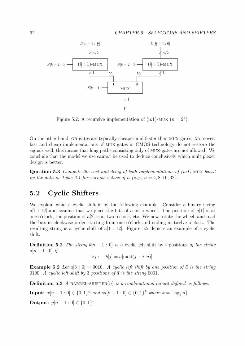
62 CHAPTER 5. SELECTORS AND SHIFTERS
S[k − 1]
(n2
: 1)-mux
n/2
1
S[k − 2 : 0]
D[n
2− 1 : 0]
(n2
: 1)-mux
n/2
1
S[k − 2 : 0]
D[n − 1 : n
2]
1
mux
Y
YL YR
1 0
Figure 5.2: A recursive implementation of (n:1)-mux (n = 2k).
On the other hand, or-gates are typically cheaper and faster than mux-gates. Moreover,fast and cheap implementations of mux-gates in CMOS technology do not restore thesignals well; this means that long paths consisting only of mux-gates are not allowed. Weconclude that the model we use cannot be used to deduce conclusively which multiplexerdesign is better.
Question 5.3 Compute the cost and delay of both implementations of (n:1)-mux basedon the data in Table 2.1 for various values of n (e.g., n = 4, 8, 16, 32).
5.2 Cyclic Shifters
We explain what a cyclic shift is by the following example. Consider a binary stringa[1 : 12] and assume that we place the bits of a on a wheel. The position of a[1] is atone o’clock, the position of a[2] is at two o’clock, etc. We now rotate the wheel, and readthe bits in clockwise order starting from one o’clock and ending at twelve o’clock. Theresulting string is a cyclic shift of a[1 : 12]. Figure 5.2 depicts an example of a cyclicshift.
Definition 5.2 The string b[n − 1 : 0] is a cyclic left shift by i positions of the stringa[n− 1 : 0] if
∀j : b[j] = a[mod(j − i, n)].
Example 5.2 Let a[3 : 0] = 0010. A cyclic left shift by one position of ~a is the string0100. A cyclic left shift by 3 positions of ~a is the string 0001.
Definition 5.3 A barrel-shifter(n) is a combinational circuit defined as follows:
Input: x[n− 1 : 0] ∈ 0, 1n and sa[k − 1 : 0] ∈ 0, 1k where k = dlog2 ne.
Output: y[n− 1 : 0] ∈ 0, 1n.
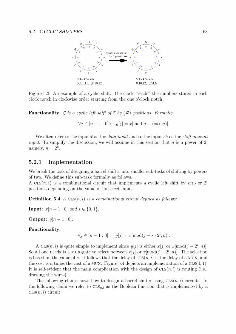
5.2. CYCLIC SHIFTERS 63
910
1112
1
23
4
56
7
8
"clock"reads:5,3,1,11,...,8,10,12
"clock"reads:8,10,12,...,2,4,6
910
1112
1
23
4
56
7
8
5
31
11
972
46
8
10 12
5
3111
97
2
4 6 8
1012
rotate clockwiseby 3 positions
Figure 5.3: An example of a cyclic shift. The clock “reads” the numbers stored in eachclock notch in clockwise order starting from the one o’clock notch.
Functionality: ~y is a cyclic left shift of ~x by 〈 ~sa〉 positions. Formally,
∀j ∈ [n− 1 : 0] : y[j] = x[mod(j − 〈 ~sa〉, n)].
We often refer to the input ~x as the data input and to the input ~sa as the shift amountinput. To simplify the discussion, we will assume in this section that n is a power of 2,namely, n = 2k.
5.2.1 Implementation
We break the task of designing a barrel shifter into smaller sub-tasks of shifting by powersof two. We define this sub-task formally as follows.A cls(n, i) is a combinational circuit that implements a cyclic left shift by zero or 2i
positions depending on the value of its select input.
Definition 5.4 A cls(n, i) is a combinational circuit defined as follows:
Input: x[n− 1 : 0] and s ∈ 0, 1.
Output: y[n− 1 : 0].
Functionality:
∀j ∈ [n− 1 : 0] : y[j] = x[mod(j − s · 2i, n)].
A cls(n, i) is quite simple to implement since y[j] is either x[j] or x[mod(j − 2i, n)].So all one needs is a mux-gate to select between x[j] or x[mod(j − 2i, n)]. The selectionis based on the value of s. It follows that the delay of cls(n, i) is the delay of a mux, andthe cost is n times the cost of a mux. Figure 5.4 depicts an implementation of a cls(4, 1).It is self-evident that the main complication with the design of cls(n.i) is routing (i.e.,drawing the wires).
The following claim shows how to design a barrel shifter using cls(n, i) circuits. Inthe following claim we refer to clsn,i as the Boolean function that is implemented by acls(n, i) circuit.
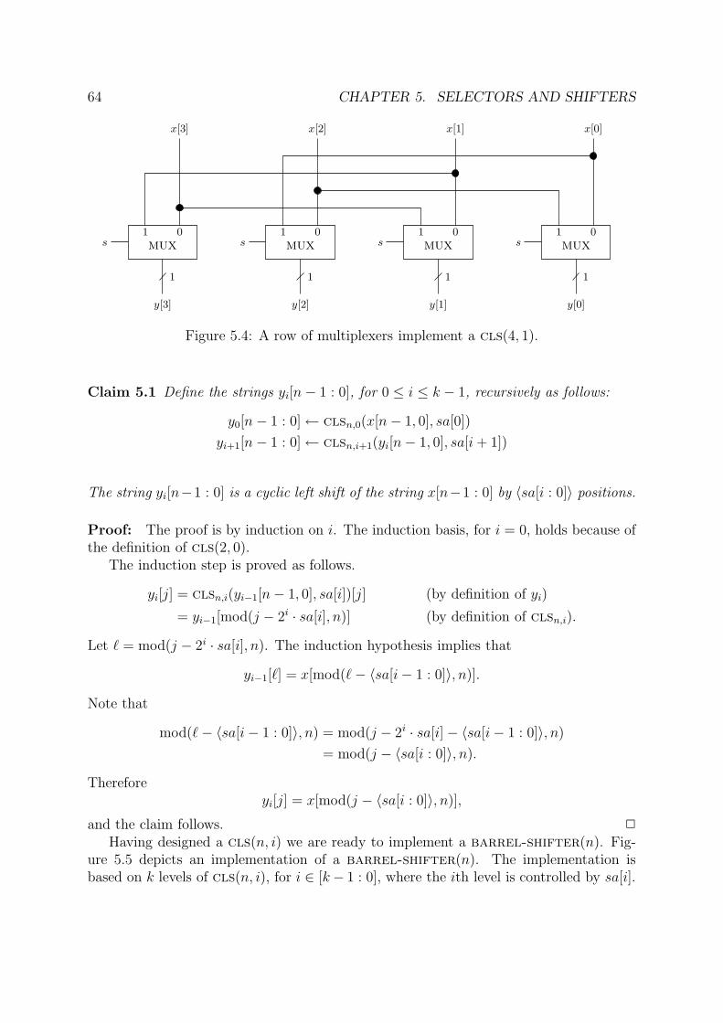
64 CHAPTER 5. SELECTORS AND SHIFTERS
1
s1 0
mux
y[2]
1
s1 0
mux
y[1]
s
1
y[3]
1
s1 0
mux
y[0]
1 0
mux
x[0]x[1]x[2]x[3]
Figure 5.4: A row of multiplexers implement a cls(4, 1).
Claim 5.1 Define the strings yi[n− 1 : 0], for 0 ≤ i ≤ k − 1, recursively as follows:
y0[n− 1 : 0]← clsn,0(x[n− 1, 0], sa[0])
yi+1[n− 1 : 0]← clsn,i+1(yi[n− 1, 0], sa[i + 1])
The string yi[n−1 : 0] is a cyclic left shift of the string x[n−1 : 0] by 〈sa[i : 0]〉 positions.
Proof: The proof is by induction on i. The induction basis, for i = 0, holds because ofthe definition of cls(2, 0).
The induction step is proved as follows.
yi[j] = clsn,i(yi−1[n− 1, 0], sa[i])[j] (by definition of yi)
= yi−1[mod(j − 2i · sa[i], n)] (by definition of clsn,i).
Let ` = mod(j − 2i · sa[i], n). The induction hypothesis implies that
yi−1[`] = x[mod(`− 〈sa[i− 1 : 0]〉, n)].
Note that
mod(`− 〈sa[i− 1 : 0]〉, n) = mod(j − 2i · sa[i]− 〈sa[i− 1 : 0]〉, n)
= mod(j − 〈sa[i : 0]〉, n).
Thereforeyi[j] = x[mod(j − 〈sa[i : 0]〉, n)],
and the claim follows. 2
Having designed a cls(n, i) we are ready to implement a barrel-shifter(n). Fig-ure 5.5 depicts an implementation of a barrel-shifter(n). The implementation isbased on k levels of cls(n, i), for i ∈ [k− 1 : 0], where the ith level is controlled by sa[i].
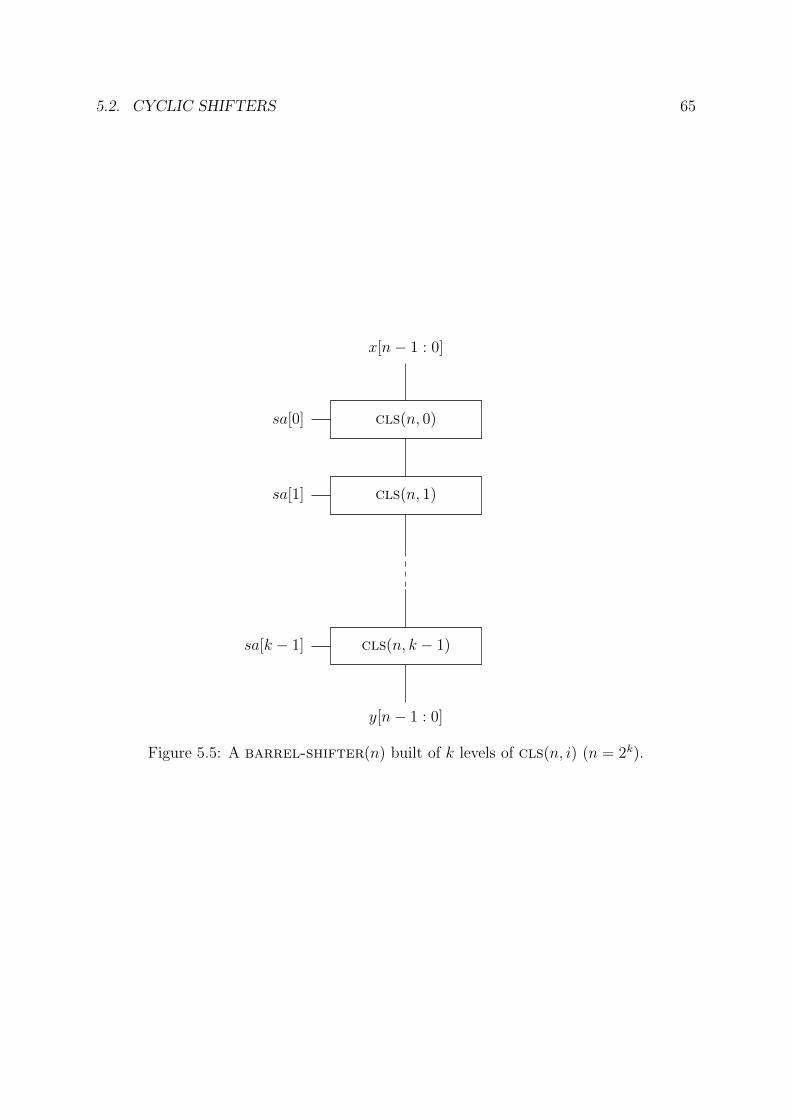
5.2. CYCLIC SHIFTERS 65
cls(n, 0)sa[0]
cls(n, 1)sa[1]
cls(n, k − 1)sa[k − 1]
x[n− 1 : 0]
y[n− 1 : 0]
Figure 5.5: A barrel-shifter(n) built of k levels of cls(n, i) (n = 2k).

66 CHAPTER 5. SELECTORS AND SHIFTERS
Question 5.4 This question deals with the design of the barrel-shifter(n) depictedin Figure 5.5.
1. Prove the correctness of the design.
2. Is the functionality preserved if the order of the levels is changed?
3. Analyze the cost and delay of the design.
4. Prove the asymptotic optimality of the delay of the design.
5. Prove a lower bound on the cost of a combinational circuit that implements a cyclicshifter.
5.3 Logical Shifters
Logical shifting is used for shifting binary strings that represent unsigned integers inbinary representation. Shifting to the left by s positions corresponds to multiplying by2s followed by modulo 2n. Shifting to the right by s positions corresponds to division by2s followed by truncation.
A bi-directional logical shifter is defined as follows.
Definition 5.5 A log-shift(n) is a combinational circuit defined as follows:
Input:
• x[n− 1 : 0] ∈ 0, 1n,
• sa[k − 1 : 0] ∈ 0, 1k, where k = dlog2 ne, and
• ` ∈ 0, 1.
Output: y[n− 1 : 0] ∈ 0, 1n.
Functionality: The output ~y is a logical shift of ~x by 〈 ~sa〉 positions. The direction ofthe shift is determined by `. Formally, If ` = 1, then perform a logical left shift asfollows:
y[n− 1 : 0]4
= x[n− 1− 〈 ~sa〉 : 0] · 0〈 ~sa〉.
If ` = 0, then perform a logical right shift as follows:
y[n− 1 : 0]4
= 0〈 ~sa〉 · x[n− 1 : 〈 ~sa〉].
Example 5.3 Let x[3 : 0] = 0010. If sa[1 : 0] = 10 and ` = 1, then log-shift(4)outputs y[3 : 0] = 1000. If ` = 0, then the output equals y[3 : 0] = 0000.

5.3. LOGICAL SHIFTERS 67
5.3.1 Implementation
As in the case of cyclic shifters, we break the task of designing a logical shifter intosub-tasks of logical shifts by powers of two.
Loosely speaking, an lbs(n, i) is a logical bi-directional shifter that outputs one ofthree possible strings: the input shifted to the left by 2i positions, the input shifted to theright by 2i positions, or the input without shifting. We now formally define this circuit.
Definition 5.6 An lbs(n, i) is a combinational circuit defined as follows:
Input: x[n− 1 : 0] and s, ` ∈ 0, 1.
Output: y[n− 1 : 0].
Functionality: Define x′[n− 1 + 2i : −2i] ∈ 0, 1n+2·2i
as follows:
x′[j]4
=
x[j] if n > j ≥ 0
0 otherwise.
The value of the output y[n− 1 : 0] is specified by
∀j ∈ [n− 1 : 0] : y[j] = x′[j + (−1)` · s · 2i]. (5.1)
Note that the vector ~x′ is an extension of the input ~x in which 2i zeros are paddedto the left and to the right of ~x. The indexes of the bit string ~x′ are also negative; thisnon-standard indexing is very useful in the context of logical shifters. It enables us tovery easily express the fact that, in a logical shift, zeros are padded to one of the sides ofthe output.
The role of ` in Equation 5.1 is to determine if the shift is a left shift or a right shift.If ` = 1 then (−1)` = −1, and the shift is a left shift (since increasing indexes from j− 2i
to j has the effect of a left shift). If ` = 0, then (−1)` = 1, and decreasing indexes fromj + 2i to j has the effect of a right shift.
The role of s in Equation 5.1 is to determine if a shift (in either direction) takes placeat all. If s = 0, then y[j] = x[j], and no shift takes place. If s = 1, then the direction ofthe shift is determined by `.
A bit-slice of an implementation of an lbs(n, i) is depicted in Figure 5.6. By the term“bit-slice” we mean that the figure depicts only how a single output bit y[j] is computed.The whole circuit is obtained by combining such circuits for every output bit y[j]. Wedo not depict the whole circuit to avoid a messy figure with lots of wires that are hardto follow.
Figure 5.6 depicts a circuit for computing y[j] that consists of two blocks.
1. The first block is a (3 : 1)-mux. Since 3 is not a power of 2, such a multiplexercan be constructed by a “pruned” tree-like construction. On the other hand, manylibraries contain a (3 : 1)-mux as a basic gate; in such cases we can simply considera (3 : 1)-mux as a basic gate. In either case, a (3 : 1)-mux is a simple circuit with aconstant number of inputs and outputs, so the best option can be easily determinedbased on the technology at hand.

68 CHAPTER 5. SELECTORS AND SHIFTERS
22 0
x′[j − 2i]
1
x′[j + 2i]
y[j]
2
x[j]
decodings, ` (3 : 1)-mux
Figure 5.6: A bit-slice of an implementation of lbs(n, i).
2. The second block is a decoding circuit. This circuit is not a decoder as definedin Chapter 4. Instead, this is a simple circuit that is input two bits (` and s)and outputs two bits. The output of the decoding circuit controls the selectionperformed by the (3 : 1)-mux. The decoding must cause the (3 : 1)-mux to selectthe correct input based on the values of s and `. We leave it as an exercise to designthe decoding circuit.
Question 5.5 This question deals with various aspects and details concerning the designof a logical shifter.
1. Design a “pruned” tree-like (3 : 1)-mux.
2. Design the decoding box depicted in Figure 5.6.
3. Show how lbs(n, i) circuits can be cascaded to obtain a log-shift(n). Hint: followthe design of a barrel-shifter(n).
5.4 Arithmetic Shifters
Arithmetic shifters are used for shifting binary strings that represent signed integers intwo’s complement representation. Since left shifting is the same in logical shifting and inarithmetic shifting, we discuss only right shifting (i.e., division by a power of 2).
An arithmetic right shifter is defined as follows.
Definition 5.7 An arith-shift(n) is a combinational circuit defined as follows:
Input: x[n− 1 : 0] ∈ 0, 1n and sa[k − 1 : 0] ∈ 0, 1k, where k = dlog2 ne.
Output: y[n− 1 : 0] ∈ 0, 1n.
Functionality: The output ~y is a (sign-extended) arithmetic right shift of ~x by 〈 ~sa〉positions. Formally,
y[n− 1 : 0]4
= x[n− 1]〈 ~sa〉 · x[n− 1 : 〈 ~sa〉].
5.5. SUMMARY 69
Example 5.4 Let x[3 : 0] = 1001. If sa[1 : 0] = 10, then arith-shift(4) outputsy[3 : 0] = 1110.
Question 5.6 Consider the definitions of cls(n, i) and lbs(n, i). Suggest an analogousdefinition ars(n, i) for arithmetic right shift (i.e., modify the definition of ~x′ and use (2 :1)-muxs). Suggest an implementation of an arithmetic right shifter based on cascadingars(n.i) circuits.
5.5 Summary
We began this chapter by defining (n : 1)-multiplexers. We presented two optimal im-plementations. One implementations is based on a decoder, the other implementation isbased on a tree of multiplexers.
We continued by defining three types of shifts: cyclic, logical, and arithmetic shifts.The method we propose for designing such shifters is to cascade a logarithmic number ofshifters (with parameter i) that either perform a shift by 2i positions or no shift at all.

70 CHAPTER 5. SELECTORS AND SHIFTERS

Chapter 6
Priority encoders
Contents
6.1 Big Endian vs. Little Endian . . . . . . . . . . . . . . . . . . 72
6.2 Priority Encoders . . . . . . . . . . . . . . . . . . . . . . . . . 73
6.2.1 Implementation of u-penc(n) . . . . . . . . . . . . . . . . . . . 75
6.2.2 Implementation of b-penc . . . . . . . . . . . . . . . . . . . . . 77
6.3 Summary . . . . . . . . . . . . . . . . . . . . . . . . . . . . . . 80
Preliminary questions
1. Suppose that many devices wish to transmit data along a shared bus. How doesthe bus controller decide which device gets to use the bus?
2. Consider the binary fraction 0.000010101. In many cases, an arithmetic unit issupposed to shift the fraction so that its value is in the range [1/2, 1) (this is oftencalled normalization). How is the shift amount computed?
71

72 CHAPTER 6. PRIORITY ENCODERS
In this chapter we present designs of an important combinational module called pri-ority encoders. Priority encoders have many uses, among them: (1) allocating usage ofa shared resource according to a policy that is defined by priorities, and (2) determiningthe required amount of left shift needed to normalize a fraction so that it represents anumber in the interval [1/2, 1).
We begin this chapter with a discussion of the confusion that may be caused byinterchanging bit orders in which the least significant bit appears first and orders inwhich the most significant bit appears first.
6.1 Big Endian vs. Little Endian
A long standing source of confusion is the order of bits in binary strings. This issue isvery important when strings of bits are serially communicated or stored in memories.Consider the following two scenarios.
In the first setting Alice wishes to send to Bob a binary string a[n − 1 : 0]. Thechannel that Alice and Bob use for communication is a serial channel. This means thatAlice can only send one bit at a time. Now Alice has two “natural” choices:
• She can send a[n−1] first and a[0] last. Namely, she can send the bits in descendingindex order. This order is often referred to as most significant bit first or just MSBfirst.
• She can send a[0] first and a[n− 1] last. Namely, she can send the bits in ascendingindex order. This order is often referred to as least significant bit first or just LSBfirst.
In the second setting computer words are stored in memory. A memory is a vector ofstorage places. We denote this vector by M [0], M [1], . . .. Suppose that each storage placeis capable of storing a byte (i.e., 8 bits). The typical word size in modern computers is32 bits (and even 64 bits). This means that a word is stored in 4 memory slots. Thequestion is how do we store a word a[31 : 0] in 4 memory slots?
Obviously, it is a good idea to store the word in 4 consecutive slots, say M [i : i + 3].There are two “natural” options. In the first option storage is as follows:
M [i]← a[31 : 24]
M [i + 1]← a[23 : 16]
M [i + 2]← a[15 : 8]
M [i + 3]← a[7 : 0].
This option is referred to as Big Endian.
In the second option storage is as follows:

6.2. PRIORITY ENCODERS 73
M [i]← a[0 : 7]
M [i + 1]← a[8 : 15]
M [i + 2]← a[16 : 23]
M [i + 3]← a[24 : 31].
This option is referred to as Little Endian. Note that, for the sake of aesthetics, we usedincreasing bit indexes in the second option.
It is highly recommended that you read the treatise “On holy wars and a plea forpeace” by Danny Cohen (URLs have short lives, so I hope that you can find Cohen’streatise in http://www.networksorcery.com/enp/ien/ien137.txt). It was Danny Co-hen who coined the terms Big Endian and Little Endian.
Each of these options has certain advantages and disadvantages. For example, ifan architecture supports multiple word lengths, then it is convenient to have the mostsignificant bit (MSB) stored in a fixed position relative to the address of the word (inour example we can see that in Big Endian the MSB is stored in M [i] regardless of thenumber of bytes in ~a.) On the other hand, if multiple word lengths are supported and wewish to add a half word (i.e., two-byte string) with a word (i.e., four-byte string), thenLittle Endian may simplify the task of aligning the two words (i.e., making sure that bitsof the same weight are placed in identical offsets).
It is of no surprise that both conventions are used in commercial products. Archi-tectures from the X86 family (such as Intel processors) use Little Endian byte ordering,while Motorola 68000 CPUs follow the Big Endian convention. Interestingly, the Power-PC supports both! Nevertheless, operating systems also follow different conventions:Microsoft operating systems follow Little Endian and Apple operating systems follow BigEndian. So a MAC with a Power-PC CPU that runs an Apple operating system runs inBig Endian mode.
This confusion spreads beyond hardware to software (e.g., Java uses Big Endian) andto file formats (e.g., GIFF uses Little Endian and JPEG uses Big Endian).
What does this story have to do with us? You might have noticed that we use bothascending indexes and descending indexes (e.g. a[n− 1 : 0] vs. a[0 : n− 1]) to denote thesame string. These two conventions are simply an instance of the Big Endian vs. LittleEndian controversy.
Following Oliver Swift (at the risk of not obeying Danny Cohen’s plea), we use bothascending and descending bit orders according to the task we are considering. Whenconsidering strings that represent integers in binary representation, descending indexesare used (i.e., leftmost bit is the MSB). However in many parts of this chapter ascendingindexes are used; the reason is to simplify handling of indexes in the text. We can onlyhope that this simplification does not lead to confusion.
6.2 Priority Encoders
Consider a binary string x[0 : n − 1]. (Note that we use ascending indexes here! So theindex of the leftmost bit is 0.) The index of the leading one is the index of the leftmost

74 CHAPTER 6. PRIORITY ENCODERS
non-zero bit in x[0 : n− 1]. We often abbreviate and refer to the index of the leading onesimply as the leading one. Formally,
Definition 6.1 The leading one of a binary string x[0 : n− 1] is defined by
leading-one(x[0 : n− 1])4
=
mini | x[i] = 1 if x[0 : n− 1] 6= 0n
n otherwise.
Example 6.1 Consider the string x[0 : 6] = 0110100. The leading one is the index [1].Note that indexes are in ascending order and that x[0] is the leftmost bit.
The following claim follows immediately from the definition of the leading one.
Claim 6.1 For every binary string ~a = a[n− 1 : 0]
leading-one(~a) = leading-one(~a · 1).
A priority encoder is a combinational circuit that computes the leading one. Weconsider two types of priority encoders: A unary priority encoder outputs the leadingone in unary representation. A binary priority encoder outputs the leading one in binaryrepresentation.
Definition 6.2 A binary string x[0 : n− 1] represents a number in unary representationif x[0 : n−1] ∈ 1∗ ·0∗. The value represented in unary representation by the binary string1i · 0j is i.
Example 6.2 The binary string 01001011 does not represent a number in unary rep-resentation. Only a string that is obtained by concatenating an all-ones string with anall-zeros string represents a number in unary representation.
Before we define a unary priority encoder, we define a parallel prefix or circuit.
Definition 6.3 A parallel prefix or circuit of length n is a combinational circuit specifiedas follows.
Input: x[0 : n− 1].
Output: y[0 : n− 1].
Functionality:y[i] = or(x[0 : i]).
We denote parallel prefix or circuit of length n by ppc–or(n).We denote unary priority encoder by u-penc(n) and define it as follows. Note that
the output of u-penc(n) is simply the inversion of the outputs of ppc–or(n).
Definition 6.4 A unary priority encoder u-penc(n) is a combinational circuit specifiedas follows.

6.2. PRIORITY ENCODERS 75
Input: x[0 : n− 1].
Output: y[0 : n− 1].
Functionality: The output y[0 : n− 1] is the unary representation of leading-one(~x),namely,
y[i] = inv(or(x[0 : i])).
Example 6.3 Consider the string x[0 : 6] = 0110100. The output of a ppc–or(7) is0111111. The output of a u-penc(7) is 1000000.
Example 6.4 If ~x 6= 0n, then the output of u-penc(n) satisfies y[0 : n− 1] = 1j · 0n−j,where j = mini | x[i] = 1. If ~x = 0n, then ~y = 1n and ~y is a unary representation of n.
We denote binary priority encoder by b-penc(n) and define it as follows.
Definition 6.5 A binary priority encoder b-penc(n) is a combinational circuit specifiedas follows.
Input: x[0 : n− 1].
Output: y[k : 0], where k = blog2 nc. (Note that if n = 2`, then k = `.)
Functionality:〈~y〉 = leading-one(~x)
Note that if n = 2k, then the length of the output of a b-penc(n) is k + 1 bits;otherwise, the number n could not be represented by the output.
Example 6.5 Given input x[0 : 5] = 000101, a u-penc(6) outputs y[0 : 5] = 111000,and b-penc(6) outputs y[2 : 0] = 011.
6.2.1 Implementation of u-penc(n)
We can design a unary priority encoder by inverting the outputs of a parallel prefixppc–or(n). A brute force design of a ppc–or(n) uses a separate or-tree for each outputbit. The delay of such a design is O(log n) and the cost is O(n2). The issue of efficientlycombining these trees will be discussed in detail when we discuss parallel prefix compu-tation in the context of fast addition. In the meantime, we present here a (non-optimal)design based on divide-and-conquer.
The method of divide-and-conquer is applicable for designing a ppc–or(n). We applydivide-and-conquer in the following recursive design. If n = 1, then ppc–or(1) is thetrivial design in which y[0]← x[0]. A recursive design of ppc–or(n) for n > 1 that is apower of 2 is depicted in Figure 6.1. Proving the correctness of the proposed ppc–or(n)design is a simple exercise in associativity of orn, so we leave it as a question.
Question 6.1 This question deals with the recursive design of the ppc–or(n) circuitdepicted in Figure 6.1.

76 CHAPTER 6. PRIORITY ENCODERS
n/2
ppc–or(n
2)
n/2
n/2 n/2
ppc–or(n
2)
or(n
2)
y[n
2: n− 1]
x[0 : n
2− 1] x[n
2: n− 1]
1
y[0 : n
2− 1]
n/2 [n
2− 1] yR[n
2: n− 1]
Figure 6.1: A recursive implementation of ppc–or(n).
1. Prove the correctness of the design.
2. Extend the design for values of n that are not powers of 2.
3. Analyze the delay of the design.
4. Prove the asymptotic optimality of the delay of the design.
Cost analysis. The cost c(n) of the ppc–or(n) depicted in Figure 6.1 satisfies thefollowing recurrence equation.
c(n) =
0 if n=1
2 · c(n2) + (n/2) · c(or) otherwise.
It follows that
c(n) = 2 · c(n
2) + Θ(n)
= Θ(n · log n).
The following question deals with the asymptotic optimality of the ppc–or(n) designdepicted in Figure 6.1.
Question 6.2 Prove a lower bound on the cost of a parallel prefix computation circuitppc–or(n).
In the chapter on fast addition we will present a cheaper implementation of ppc–or(n)(with logarithmic delay).

6.2. PRIORITY ENCODERS 77
6.2.2 Implementation of b-penc
In this section we present two designs for a binary priority encoder. The first designis based on a reduction to a unary priority encoder. The second design is based ondivide-and-conquer.
Reduction to ppc–or
Consider an input x[0 : n − 1] to a binary priority encoder. If ~x = 0n, then the outputshould equal bin(n). If ~x 6= 0n, then let j = mini | x[i] = 1. The output ~y of ab-penc(n) should satisfy 〈~y〉 = j. Our design is based on the observation that theoutput u[0 : n − 1] of a ppc–or(n) satisfies ~u = 0j · 1n−j. In Figure 6.2 we depict areduction from the task of computing ~y to the task of computing ~u.
n
encoder(k + 1)
zero-test(n)
1z
nn
k + 1 k + 1
2k+1
u[0 : n− 1]
diff(n)
ppc–or(n)
u′[0 : n− 1] n
x[0 : n− 1]
y′[k : 0]bin(n)
y[k : 0]
mux(k + 1)
pad-zeros(2k+1)
u”[0 : 2k+1− 1]
Figure 6.2: A binary priority encoder based on a unary priority encoder.
The stages of the reduction are as follows. We first assume that the input x[n− 1 : 0]is not 0n and denote leading-one(~x) by j. We then deal with the case that ~x = 0n
separately.
1. The input ~x is fed to a ppc–or(n) that outputs the string u[0 : n− 1] = 0j · 1n−j.

78 CHAPTER 6. PRIORITY ENCODERS
2. A difference circuit is fed by ~u and outputs the string u′[0 : n − 1]. The stringu′[0 : n− 1] is defined as follows:
u′[i] =
u[0] if i = 0
u[i]− u[i− 1] otherwise.
Note that the output u′[0 : n− 1] satisfies:
u′[0 : n− 1] = 0j · 1 · 0n−1−j.
Hence ~u′ constitutes a 1-out-of-n representation of the index of the leading one(provided that ~x 6= 0n).
3. If n is not a power of 2, then obtain the string u′′[0 : 2k+1 − 1] from ~u′ by paddingzeros from the right as follows:
u′′[0 : n− 1]← u′[0 : n− 1] u′′[n : 2k+1 − 1]← 02k−n.
Namely, u′′[0 : 2k+1 − 1] = 0j · 1 · 02k+1−1. (Recall that k = blog2 nc.) Note that thecost and delay of padding zeros is zero.
4. The string u′′[0 : 2k+1 − 1] is input to an encoder(k + 1). The encoder outputsthe string y′[k : 0] that satisfies 〈~y′〉 equals the index of the bit in ~u′′ that equalsone. Namely, 〈~y′〉 = j, which is the desired output if ~x 6= 0n. In the next item dealalso with the case of an all-zeros input.
5. The input x[n − 1 : 0] is fed to a zero-tester that outputs 1 if ~x = 0n. In this case,the output y[k : 0] should satisfy 〈~y〉 = n. The selection between bin(n) and ~y′ isperformed by the multiplexer according to the output of the zero-tester.
Cost and delay analysis. The cost of the binary priority encoder depicted in Fig-ure 6.2 satisfies:
c(n) = c(ppc–or(n)) + c(diff(n)) + c(encoder(k)) + c(mux(k)) + c(zero-test(n))
= c(ppc–or(n)) + Θ(n).
Hence, the cost of the reduction from a binary priority encoder to a unary priority encoderis linear. This implies that if we knew how to implement a linear cost ppc–or(n) thenwe would have a linear cost b-penc(n).
The delay of the binary priority encoder depicted in Figure 6.2 satisfies:
d(n) = maxd(ppc–or(n)) + d(diff(n)) + d(encoder(k)), d(zero-test(n))+ d(mux)
= d(ppc–or(n)) + Θ(log n).
Hence, the delay of the reduction from a binary priority encoder to a unary priorityencoder is logarithmic.

6.2. PRIORITY ENCODERS 79
A divide-and-conquer implementation
We now present a divide-and-conquer design. For simplicity, assume that n = 2k.Figure 6.3 depicts a recursive design for a binary priority encoder. Consider an input
x[0 : n− 1]. We partition it into two halves: the left part x[0 : n2− 1] and the right part
x[n2
: n− 1]. Each of these two parts is fed to a binary priority encoder with n/2 inputs.We denote the outputs of these binary priority encoders by yL[k − 1 : 0] and yR[k − 1 : 0].The final output y[k : 0] is computed as follows: y[k] = 1 iff yL[k − 1] = yR[k − 1] = 1,y[k−1] = and(yL[k−1], inv(yR[k−1])), and y[k−2 : 0] equals yL[k − 2 : 0] if yL[k−1] = 0and yR[k − 2 : 0] otherwise. We now prove the correctness of the binary priority encoder
k − 1
b-penc(n
2) b-penc(n
2)
k
n/2 n/2
k − 1 k − 1
and
y[k]
yR[k − 1]
and
y[k − 1]
inv(yR[k − 1])
mux(k − 1)
y[k − 2 : 0]
x[0 : n
2− 1] x[n
2: n− 1]
0 1
yL[k − 2 : 0] yR[k − 2 : 0]
yR[k − 1]
k
yL[k − 1]
Figure 6.3: A recursive implementation of a binary priority encoder.
design based on divide-and-conquer. Note that we omitted a description for n = 2. Weleave the recursion basis as an exercise.
Claim 6.2 The design depicted in Figure 6.3 is a binary priority encoder.
Proof: The proof is by induction. We assume that we have a correct design for n = 2so the induction basis holds. We proceed with the induction step. We consider threecases:
1. x[0 : n2− 1] 6= 0n/2. By the induction hypothesis, the required output in this case
equals 0 · ~yL. Note that yL[k− 1] = 0 since the index of the leading one is less thann/2. It follows that y[k] = y[k − 1] = 0 and y[k − 2 : 0] = yL[k − 2 : 0]. Hence〈~y〉 = 〈 ~yL〉, and the output equals the index of the leading one, as required.
2. x[0 : n2− 1] = 0n/2 and x[n
2: n− 1] 6= 0n/2. In this case the index of the leading one
is n/2+〈 ~yR〉. By the induction hypothesis, we have yL[k−1] = 1 and yR[k−1] = 0.It follows that y[k] = 0, y[k − 1] = 1, and y[k − 2 : 0] = yR[k − 2 : 0]. Hence〈~y〉 = 2k−1 + 〈 ~yR〉, as required.
3. x[0 : n2− 1] = 0n/2 and x[n
2: n − 1] = 0n/2. By the induction hypothesis, we
have yL[k − 1 : 0] = yR[k − 1 : 0] = 1 · 0k−1. Hence y[k] = 1, y[k − 1] = 0, andy[k − 2 : 0] = 0k−1, as required.
80 CHAPTER 6. PRIORITY ENCODERS
Since the design is correct in all three cases, we conclude that the design is correct. 2
Cost and delay analysis. The cost of the binary priority encoder depicted in Fig-ure 6.3 satisfies (recall that n = 2k):
c(b-penc(n)) =
c(nor) + c(and) + c(inv) if n=2
2 · c(b-penc(n/2)) + 2 · c(and) + (k − 1) · c(mux) otherwise.
Consider the substitution γ(k) = c(2k). Then γ(k) satisfies the recurrence
γ(k) = 2 · γ(k − 1) + Θ(k).
This recurrence is identical to the recurrence in Equation 4.1. Hence γ(k) = Θ(2k) andc(b-penc(n)) = Θ(n). This implies the asymptotic optimality of the design.
The delay of the binary priority encoder depicted in Figure 6.3 satisfies:
d(b-penc(n)) =
tpd(nor) if n=2
d(b-penc(n/2)) + maxd(mux) + d(and) otherwise.
Hence, the delay is logarithmic, and the design is asymptotically optimal also with respectto delay.
6.3 Summary
In this section we presented designs of priority encoders. Priority encoders are circuitsthat compute the position of a leading one in a binary string. We considered two typesof priority encoders: unary and binary. The difference between these two types of pri-ority encoders is in how the position of the leading one is represented (i.e. in binaryrepresentation or in unary representation).
We first considered unary priority encoders. In the unary case, it is more convenientto consider parallel prefix or circuits. The only difference between these two circuitsis the inversion of the outputs. We presented a divide-and-conquer design for a parallelprefix or circuit ppc–(or)(n). When we discuss fast addition we will return to thiscircuit and present an even cheaper design.
We then considered binary priority encoders. Two designs were presented. Thefirst one is simply a reduction to ppc–(or)(n). The overhead in cost is linear and theoverhead in delay is logarithmic. Hence, this design leads to an asymptotically optimalbinary priority encoder provided that a linear cost and logarithmic delay ppc–(or)(n)design is used.
The second binary priority encoder design is a divide-and-conquer design. The cost ofthis design is linear cost and the delay is logarithmic, hence this design is asymptoticallyoptimal.

Chapter 7
Half-Decoders
Contents
7.1 Specification . . . . . . . . . . . . . . . . . . . . . . . . . . . . 82
7.2 Preliminaries . . . . . . . . . . . . . . . . . . . . . . . . . . . . 82
7.3 Implementation . . . . . . . . . . . . . . . . . . . . . . . . . . 84
7.4 Correctness . . . . . . . . . . . . . . . . . . . . . . . . . . . . . 84
7.5 Cost and delay analysis . . . . . . . . . . . . . . . . . . . . . . 86
7.6 Application . . . . . . . . . . . . . . . . . . . . . . . . . . . . . 87
7.7 Summary . . . . . . . . . . . . . . . . . . . . . . . . . . . . . . 87
Preliminary questions
1. How can we reduce the task of a bi-directional logical shift to a cyclic left shift?
2. Is it easy to compare a number x represented in unary representation with a constanti?
81

82 CHAPTER 7. HALF-DECODERS
In this chapter we deal with the design of half-decoders. Recall that a decoder isa combinational circuit that computes a 1-out-of-2n representation of a given binarynumber. A half-decoder computes a unary representation of a given binary number.Half-decoders can be used for reducing the task of a logical shift to a cyclic shift.
7.1 Specification
Definition 7.1 A half-decoder with input length n is a combinational circuit defined asfollows:
Input: x[n− 1 : 0].
Output: y[0 : 2n − 1]
Functionality:y[0 : 2n − 1] = 1〈x[n−1:0]〉 · 02n−〈x[n−1:0]〉.
We denote a half-decoder with input length n by h-dec(n).
Example 7.1 • Consider a half-decoder h-dec(3). Given x[2 : 0] = 101, h-dec(3)outputs y[0 : 7] = 11111000.
• Given ~x = 0n, h-dec(n) outputs ~y = 02n
.
• Given ~x = 1n, h-dec(n) outputs ~y = 12n−1 · 0.
Remark 7.1 Observe that y[2n − 1] = 0, for every input string. One could omit the bity[2n − 1] from the definition of a half-decoder. We left it in to make the description ofthe design slightly simpler.
The next question deals with designing a half-decoder using a decoder and a unarypriority encoder. The delay of the resulting design is too big.
Question 7.1 Suggest an implementation of a half-decoder based on a decoder and aunary priority encoder. Analyze the cost and delay of the design. Is it asymptoticallyoptimal with respect to cost or delay?
7.2 Preliminaries
In this section we present a few claims that are used in the design of asymptoticallyoptimal half-decoders.The following claim follows trivially from the definition of a half-decoder.
Claim 7.1y[i] = 1⇐⇒ i < 〈~x〉.

7.2. PRELIMINARIES 83
Assume that the binary string z[0 : n−1] represents a number in unary representation(namely, ~z = 1j · 0n−j). Let wt(~z) denote the value represented by ~z in unary represen-tation. The following claim shows that it is easy to compare wt(~z) with a fixed constanti ∈ [0, n− 1]. (By easy we mean that it requires constant cost and delay.)
Claim 7.2 For i ∈ [0 : n− 1]:
wt(~z) < i⇐⇒ z[i − 1] = 0
wt(~z) > i⇐⇒ z[i] = 1
wt(~z) = i⇐⇒ z[i] = 0 and z[i− 1] = 1.
Question 7.2 Prove Claim 7.2.
Claim 7.2 gives a simple recipe for a “comparison box”. A comparison box, denotedby comp(~z, i), is a combinational circuit that compares wt(~z) and i. It has two inputs:z[i − 1] and z[i], and it has three outputs GT, EQ, LT . The outputs have the followingmeaning: GT - indicates whether wt(~z) > i, EQ - indicates whether wt(~z) = i, andLT - indicates whether wt(~z) < i. In the sequel we will only need the GT and EQoutputs. (Note that the GT output simply equals z[i] and the LT output simply equalsinv(z[i − 1])).
We now follow the technique of division with a remainder (see Claim 4.1). Considera partitioning of a string x[n − 1 : 0] according to a parameter k into two sub-strings oflength k and n− k. Namely
xL[n− k − 1 : 0] = x[n− 1 : k] and xR[k − 1 : 0] = x[k − 1 : 0].
Binary representation implies that
〈~x〉 = 2k · 〈~xL〉+ 〈~xR〉.
Namely the quotient when dividing 〈~x〉 by 2k is 〈~xL〉, and the remainder is 〈~xR〉.Consider an index i, and divide it by 2k to obtain i = 2k·q+r, where r ∈ 0, . . . , 2k−1.
(The quotient of this division is q, and r is simply the remainder.) Division by 2k can beinterpreted as partitioning the numbers into blocks, where each block consists of numberswith the same quotient. This division divides the range [2n− 1 : 0] into 2n−k blocks, eachblock is of length 2k. The quotient q can be viewed as an index of the block that i belongsto. The remainder r can be viewed as the offset of i within its block.
The following claim shows how to easily compare i and 〈~x〉 given q, r, 〈~xL〉, and 〈~xR〉.
Claim 7.3i < 〈~x〉 ⇐⇒ q < 〈~xL〉 or (q = 〈~xL〉 and r < 〈~xR〉)
The interpretation of the above claim in terms of “blocks” and “offsets” is the following.The number 〈~x〉 is a number in the range [2n−1 : 0]. The index of the block this numberbelongs to is 〈~xL〉. The offset of this number within its block is 〈~xR〉. Hence, comparisonof 〈~x〉 and i can be done in two steps: compare the block indexes, if they are different,then the number with the higher block index is bigger. If the block indexes are identical,then the offset value determines which number is bigger.

84 CHAPTER 7. HALF-DECODERS
7.3 Implementation
In this section we present an asymptotically optimal half-decoder design. Our design isa recursive divide-and-conquer design.
A h-dec(n), for n = 1 is the trivial circuit y[0] ← x[0]. We now proceed withthe recursion step. Figure 7.1 depicts a recursive implementation of a h-dec(n). Theparameter k equals k = dn
2e (in fact, to minimize delay one needs to be a bit more precise
since the paths may not be perfectly balanced for k = dn2e). The input string x[n− 1 : 0]
is divided into two strings xL[n− k− 1 : 0] = x[n− 1 : k] and xR[k− 1 : 0] = x[k− 1 : 0].These strings are fed to a half-decoders h-dec(n − k) and h-dec(k), respectively. Wedenote the outputs of the half-decoders by zL[2n−k−1 : 0] and zR[2k−1 : 0], respectively.Each of these string are fed to comparison boxes. The “rows” comparison box is fed by ~zL
and compares ~zL with i ∈ [0 : 2n−k− 1]. The “columns” comparison box is fed by ~zR andcompares ~zR with j ∈ [0 : 2k − 1]. Note that we only use the GT and EQ outputs of therows comparison box, and that we only use the GT output of the columns comparison box.(Hence the columns comparison box is trivial and has zero cost and delay.) We denotethe outputs of the rows comparison box by QGT [0 : 2n−k − 1] and QEQ[0 : 2n−k − 1].We denote the output of the columns comparison box by RGT [0 : 2k − 1]. Finally, theoutputs of the comparison boxes fed an array of 2n−k × 2k G-gates. Consider the G-gateGq,r positioned in row q and in column r. The gate Gq,r outputs y[q · 2k + r] that isdefined by
y[q · 2k + r]4
= or(QGT [q],and(QEQ[q], RGT [r])). (7.1)
Example 7.2 Let n = 4 and k = 2. Consider i = 6. The quotient and remainder of iwhen divided by 4 are 1 and 2, respectively. By Claim 7.1, y[6] = 1 iff 〈x[3 : 0]〉 > 6. ByClaim 7.3, 〈~x〉 > 6 iff (〈x[3 : 2]〉 > 1) or (〈x[3 : 2]〉 = 1 and 〈x[1 : 0]〉 > 2). It followsthat if QGT [1] = 1, then y[6] = 1. If QEQ[1] = 1, then y[6] = RGT [2].
7.4 Correctness
Claim 7.4 The design depicted in Figure 7.1 is a correct implementation of a half-decoder.
Proof: The proof is by induction on n. The induction basis, for n = 1, is trivial. Wenow prove the induction step. By Claim 7.1 it suffices to show that y[i] = 1 iff i < 〈~x〉,for every i ∈ [2n − 1 : 0]. Fix an index i and let i = q · 2k + r. By Claim 7.3,
i < 〈~x〉 ⇐⇒ (q < 〈~xL〉) or ((q = 〈~xL〉) and (r < 〈~xR〉)).
The induction hypothesis implies that:
q < 〈~xL〉 ⇐⇒ zL[q] = 1
q = 〈~xL〉 ⇐⇒ zL[q] = 0 and zL[q − 1] = 1
r < 〈~xR〉 ⇐⇒ zR[r] = 1.

7.4. CORRECTNESS 85
h-dec(k)
k
comp( ~zR, j)2k−1j=0
2k
h-dec(n−
k)
comp(~z L
,i)2
n−
k−
1i=
0
2n−k
2k
2n−k
2n−k
xR[k − 1 : 0]4
= x[k − 1 : 0]
~zR
2n−k × 2k
array of
G-gates
xL[n− k − 1 : 0]
x[n− 1 : k]
4
=n− k
~RGT
~zL
~QGT
~QEQ
Figure 7.1: A recursive implementation of h-dec(n). Note that the comparison boxescomp( ~zR, j) are trivial, since we only use their GT outputs.

86 CHAPTER 7. HALF-DECODERS
Observe that:
• The signal QGT [q] equals zL[q], and hence indicates if q < 〈~xL〉.
• The signal QEQ[q] equals and(inv(zL[q]), zL[q−1]), and hence indicates if q = 〈~xL〉.
• The signal RGT [r] equals zR[r], and hence indicates if r < 〈~xR〉.
Finally, by Eq. 7.1, y[i] = 1 iff or(QGT [q],and(QEQ[q], RGT [r])). Hence y[i] is correct,and the claim follows. 2
7.5 Cost and delay analysis
The cost of h-dec(n) satisfies the following recurrence equation:
c(h-dec(n)) =
0 if n=1
c(h-dec(k)) + c(h-dec(n− k))
+2n−k · c(EQ) + 2n · c(G) otherwise.
The cost of computing the EQ signals is c(inv) + c(and). The cost of a G-gate isc(and) + c(or). It follows that
c(h-dec(n)) = c(h-dec(k)) + c(h-dec(n− k)) + Θ(2n)
We already solved this recurrence in the case of decoders and showed that c(h-dec(n)) =Θ(2n).
The delay of h-dec(n) satisfies the following recurrence equation:
d(h-dec(n)) =
0 if n=1
maxd(h-dec(k)), d(h-dec(n− k)) + d(EQ)
+d(G) otherwise.
The delay of computing EQ as well as the delay of a G-gate is constant. Set k = d n2e,
then the recurrence degenerates to
d(h-dec(n)) = d(h-dec(n/2)) + Θ(1)
= Θ(log n).
It follows that the delay of h-dec(n) is asymptotically optimal since all the inputs belongto the cone of a half-decoder.The following question deals with the asymptotically optimal cost of a half-decoder design.
Question 7.3 Prove that every implementation of a half-decoder design must contain atleast 2n − 2 non-trivial gates. (Here we assume that every non-trivial gate has a singleoutput, and we do not have any fan-in or fan-out restrictions).
Hint: The idea is to show that all the outputs must be fed by distinct non-trivial gates.Well, we know that y[2n − 1] = 0, so that rules out one output. What about the otheroutputs? We need to show that:

7.6. APPLICATION 87
1. The other outputs are not constant - so they can’t be fed by a trivial constant gate.
2. The other outputs are distinct - so every two outputs can’t be fed by the same gate.
3. The other outputs do no equal the inputs - so they can’t be directly fed from inputgates (which are trivial gates).
It is not hard to prove the first two items. The third item is simply false! There doesexist an output bit that equals one of the input bits. Can you prove which output bit thisis? Can you prove that it is the only such output bit?
7.6 Application
In the following question half-decoders are used to implement shifters that support alltypes of shifts.
Question 7.4 CPUs often support all three types of shifting: cyclic, logical, and arith-metic shifting.
1. Write a complete specification of a shifter that can perform all three types of shifts.
2. Propose an implementation of such a shifter.
7.7 Summary
This chapter deals with the design of optimal half-decoders. A half-decoder outputs aunary representation of a binary number. Our divide-and-conquer design is a variationof a decoder design. It employs the fact that comparison with a constant is easy in unaryrepresentation.

88 CHAPTER 7. HALF-DECODERS

Chapter 8
Addition
Contents
8.1 Definition of a binary adder . . . . . . . . . . . . . . . . . . . 91
8.2 Ripple Carry Adder . . . . . . . . . . . . . . . . . . . . . . . . 91
8.2.1 Correctness proof . . . . . . . . . . . . . . . . . . . . . . . . . . 92
8.2.2 Delay and cost analysis . . . . . . . . . . . . . . . . . . . . . . 93
8.3 Carry bits . . . . . . . . . . . . . . . . . . . . . . . . . . . . . . 93
8.3.1 Redundant and non redundant representation . . . . . . . . . . 94
8.3.2 Cone of adder outputs . . . . . . . . . . . . . . . . . . . . . . . 95
8.3.3 Reductions between sum and carry bits . . . . . . . . . . . . . 95
8.4 Conditional Sum Adder . . . . . . . . . . . . . . . . . . . . . . 95
8.4.1 Motivation . . . . . . . . . . . . . . . . . . . . . . . . . . . . . 96
8.4.2 Implementation . . . . . . . . . . . . . . . . . . . . . . . . . . . 96
8.4.3 Delay and cost analysis . . . . . . . . . . . . . . . . . . . . . . 96
8.5 Compound Adder . . . . . . . . . . . . . . . . . . . . . . . . . 98
8.5.1 Implementation . . . . . . . . . . . . . . . . . . . . . . . . . . . 99
8.5.2 Correctness . . . . . . . . . . . . . . . . . . . . . . . . . . . . . 99
8.5.3 Delay and cost analysis . . . . . . . . . . . . . . . . . . . . . . 100
8.6 Summary . . . . . . . . . . . . . . . . . . . . . . . . . . . . . . 101
89
90 CHAPTER 8. ADDITION
Preliminary questions
1. What is the definition of an adder?
2. What is the smallest possible delay of an adder? Do you know of an adder thatachieves this delay?
3. Can you prove the correctness of the addition algorithm taught in elementaryschool?
4. Suppose you are given the task of adding very long numbers. Could you sharethis work with friends so that you could work on it simultaneously to speed up thecomputation?

8.1. DEFINITION OF A BINARY ADDER 91
In this chapter we define binary adders. We start by considering a Ripple CarryAdder. This is a design with linear delay and linear cost. We then present designs withlogarithmic delay but super-linear cost.
8.1 Definition of a binary adder
Definition 8.1 A binary adder with input length n is a combinational circuit specifiedas follows.
Input: A[n− 1 : 0], B[n− 1 : 0] ∈ 0, 1n, and C[0] ∈ 0, 1.
Output: S[n− 1 : 0] ∈ 0, 1n and C[n] ∈ 0, 1.
Functionality:
〈~S〉+ 2n · C[n] = 〈 ~A〉+ 〈 ~B〉+ C[0] (8.1)
We denote a binary adder with input length n by adder(n). The inputs ~A and ~B arethe binary representations of the addends. The input C[0] is often called the carry-in bit.
The output ~S is the binary representation of the sum (more precisely, ~S is the binaryrepresentation of the sum modulo 2n), and the output C[n] is often called the carry-outbit.
Question 8.1 Verify that the functionality of adder(n) is well defined. Namely, forevery A[n − 1 : 0], B[n − 1 : 0], and C[0] there exist S[n − 1 : 0] and C[n] that satisfyEquation 8.1.
Hint: Show that the set of numbers that can be represented by sums 〈 ~A〉+ 〈 ~B〉+ C[0]
equals the set of numbers that can be represented by sums 〈~S〉+ 2n · C[n].
There are many ways to implement an adder(n). In this chapter we present a fewadder(n) designs.
Question 8.2 Prove lower bounds on the cost and delay of combinational circuits thatimplement an adder(n).
8.2 Ripple Carry Adder
Ripple Carry Adders are built by chaining a row of Full-Adders. We denote a RippleCarry Adder that implements an adder(n) by rca(n). A Full-Adder is a combinationalcircuit that adds three bits and represents their sum in binary representation.
We do not discuss here how to build a Full-Adder from gates. Since a Full-Adder has aconstant number of inputs and outputs, every (reasonable) implementation has constantcost and delay. Optimizing these constants is a technology dependent issue and is notwithin the scope of our discussion.

92 CHAPTER 8. ADDITION
Definition 8.2 (Full-Adder) A Full-Adder is a combinational circuit with 3 inputsx, y, z ∈ 0, 1 and 2 outputs c, s ∈ 0, 1 that satisfies:
2c + s = x + y + z.
The output s of a Full-Adder is often called the sum output. The output c of a Full-Adderis often called the carry-out output. We denote a Full-Adder by fa.
A Ripple Carry Adder, rca(n), is built by chaining a row of n Full-Adders. Anrca(n) is depicted in Figure 8.1. Note that the carry-out output of the ith Full-Adderis denoted by c[i + 1]. The weight of c[i + 1] is 2i+1. This way, the weight of every signalis two to the power of its index. One can readily notice that an rca(n) adds numbersusing the same addition algorithm that we use for adding numbers by hand.
scfa0
S[0]
A[0]B[0]
scfa1
A[1]B[1]
C[2] S[1]C[n − 2]
scfa
n−2sc
fan−1
S[n − 2]C[n − 1]S[n − 1]C[n] C[1]
A[n − 2]B[n − 2]A[n− 1]B[n− 1]
C[0]
Figure 8.1: A Ripple Carry Adder rca(n).
8.2.1 Correctness proof
In this section we prove the correctness of an rca(n). To facilitate the proof, we use anequivalent recursive definition of rca(n). The recursive definition is as follows.
Basis: an rca(1) is simply a Full-Adder. Step: a recursive description of rca(n), forn ≥ 1, is depicted in Figure 8.2.
S[n − 2 : 0]
n-1n-1
n-1
scfa
n−1
S[n − 1]C[n]
C[0]rca(n− 1)
A[n− 1]B[n− 1]
C[n − 1]
A[n − 2 : 0]B[n − 2 : 0]
Figure 8.2: A recursive description of rca(n).
The following claim deals with the correctness of rca(n).
Claim 8.1 rca(n) is a correct implementation of adder(n).

8.3. CARRY BITS 93
Proof: The proof is by induction on n. The induction basis, for n = 1, follows directlyfrom the definition of a Full-Adder. The induction step is proved as follows.
The induction hypothesis, for n− 1, is
〈A[n− 2 : 0]〉+ 〈B[n− 2 : 0]〉+ C[0] = 2n−1 · C[n− 1] + 〈S[n− 2 : 0]〉. (8.2)
The definition of a Full-Adder states that
A[n− 1] + B[n− 1] + C[n− 1] = 2 · C[n] + S[n− 1]. (8.3)
Multiply Equation 8.3 by 2n−1 to obtain
2n−1 · A[n− 1] + 2n−1 ·B[n− 1] + 2n−1 · C[n− 1] = 2n · C[n] + 2n−1 · S[n− 1]. (8.4)
Note that 2n−1 · A[n − 1] + 〈A[n− 2 : 0]〉 = 〈A[n− 1 : 0]〉. By adding Equations 8.2and 8.4 we obtain:
2n−1·C[n−1]+〈A[n− 1 : 0]〉+〈B[n− 1 : 0]〉+C[0] = 2n·C[n]+2n−1·C[n−1]+〈S[n− 1 : 0]〉.
Cancel out 2n−1 · C[n− 1], and the claim follows. 2
8.2.2 Delay and cost analysis
The cost of an rca(n) satisfies:
c(rca(n)) = n · c(fa) = Θ(n).
The delay of an rca(n) satisfies
d(rca(n)) = n · d(fa) = Θ(n).
The answer to Question 8.2 implies that the asymptotic cost of rca(n) is optimal, butits delay is exponentially far away from the optimum delay. The clock rates in modernmicroprocessors correspond to the delay of 15-20 gates (in more aggressive designs, thecritical paths are even shorter). Most microprocessors easily add 32-bit numbers withinone clock cycle. Obviously, adders in such microprocessors are not Ripple Carry Adders.In the rest of the chapter we present faster adder(n) designs.
8.3 Carry bits
We now define the carry bits associated with the addition
〈A[n− 1 : 0]〉+ 〈B[n− 1 : 0]〉+ C[0] = 〈S[n− 1 : 0]〉+ 2n · C[n]. (8.5)
Our definition is based on the values of the signals C[n − 1 : 1] of an rca(n). Thisdefinition is well defined in light of the Simulation Theorem of combinational circuits.

94 CHAPTER 8. ADDITION
Definition 8.3 The carry bits C[n : 0] corresponding to the addition in Eq. 8.5 aredefined as the values of the stable signals C[n : 0] in an rca(n).
Note that there are n + 1 carry-bits associated with the addition defined in Equa-tion 8.5; these bits are indexed from zero to n. The first carry bit C[0] is an input, thelast carry bit C[n] is an output, and the remaining carry bits C[n − 1 : 0] are internalsignals.
We now discuss a few issues related to the definition of the carry bits and binaryaddition.
8.3.1 Redundant and non redundant representation
Consider Eq. 8.5 and let x = 〈 ~A〉 + 〈 ~B〉 + C[0]. Equation 8.5 means that the sumx admits two representations. The representation of x on the right hand side is thestandard binary representation. This representation is non-redundant. This means thatevery number that is representable by n + 1 bits has a unique representation. (Notethat we need to restrict ourselves to n + 1 bits, otherwise leading zeros create multiplerepresentations. For example: 1, 01, and 001 are different representations of the samenumber).
One nice characteristic of non-redundant representation is that comparison is easy.Suppose that X[n− 1 : 0] is a binary representation of x and that Y [n− 1 : 0] is a binaryrepresentation of y. If we wish to check if x = y, all we need to do is check if the binarystrings ~X and ~Y are identical.
The left hand side represents the same value represented by C[n] and S[n − 1 : 0].However, on the left hand side we have two binary strings and a carry-in bit. Given x,there are many possible combinations of values of 〈 ~A〉, 〈 ~B〉 and C[0] that represent x. Forexample: 8 = 4 + 3 + 1 and also 8 = 5 + 3 + 0.
We refer to such a representation as redundant representation. Comparison of val-ues represented in redundant representation is not as easy as it is with non-redundantrepresentation. For example, assume that
x = ~A + ~B
x′ = ~A′ + ~B′.
It is possible that x = x′ even though A 6= A′ and B 6= B′. Namely, in redundant repre-sentation inequality of the representations does not imply inequality of the representedvalues.
Some of you might wonder at this point whether redundant representations are usefulat all. We just saw that redundant representation makes comparison non-trivial. Theanswer is that redundant representation is most useful. Probably the most noted applica-tion of redundant representation is fast multiplication. In fast multiplication, redundantrepresentation is used for fast (redundant) addition.
We summarize this discussion by noting that an alternative way to interpret an rca(n)(or an adder(n), in general) is to say that it translates a redundant representation to anon-redundant binary representation.

8.4. CONDITIONAL SUM ADDER 95
8.3.2 Cone of adder outputs
The correctness proof of rca(n) implies that, for every 0 ≤ i ≤ n− 1,
〈A[i : 0]〉+ 〈B[i : 0]〉+ C[0] = 2i+1 · C[i + 1] + 〈S[i : 0]〉. (8.6)
Equation 8.6 implies that, for every 0 ≤ i ≤ n− 1,
〈S[i : 0]〉 = mod(〈A[i : 0]〉+ 〈B[i : 0]〉+ C[0], 2i+1).
These equations imply that the cone of each of the signals C[i + 1] and S[i] is the setof inputs corresponding to A[i : 0]
⋃B[i : 0]
⋃C[0] (see the following question).
Question 8.3 Prove that the cone of each of the signals C[i + 1] and S[i] consists of2i + 1 inputs corresponding to A[i : 0]
⋃B[i : 0]
⋃C[0].
8.3.3 Reductions between sum and carry bits
The correctness of rca(n) implies that, for every 0 ≤ i ≤ n− 1,
S[i] = xor(A[i], B[i], C[i]). (8.7)
This immediately implies that, for every 0 ≤ i ≤ n− 1,
C[i] = xor(A[i], B[i], S[i]). (8.8)
Equations 8.7 and 8.8 imply constant-time linear-cost reductions between the prob-lems of computing the sum bits S[n − 1 : 0] and computing the carry bits C[n − 1 : 0].
(This reduction uses the addends ~A and ~B.) The task of computing the sum bits isthe task of an adder. In an rca(n), the carry bit C[i] is computed first, and then thesum bit S[i] is computed according to Eq. 8.7. We will later design an asymptoticallyoptimal adder that first computes all the carry bits and then obtains the sum bits fromthe carry-bits by applying Eq. 8.7.
Question 8.4 Prove Equation 8.8.
8.4 Conditional Sum Adder
A Conditional Sum Adder is a recursive adder design that is based on divide-and-conquer.One often uses only one “level” of recursion. Namely, three adders with input length n/2are used to construct one adder with input size n.

96 CHAPTER 8. ADDITION
8.4.1 Motivation
The following “story” captures the main idea behind a conditional sum adder.
Imagine a situation in which Alice, who is positioned on Earth, holds the stringsA[k − 1 : 0], B[k − 1 : 0], C[0]. Bob, who is stationed on the Moon, holds the stringsA[n − 1 : k], B[n − 1 : k]. The goal of Alice and Bob is to jointly compute the sum〈A[n− 1 : 0]〉+ 〈B[n− 1 : 0]〉+ C[0]. They don’t care who holds the sum bits and C[n],as long as one of them does. Now, sending information from Alice to Bob is costly. Thefirst question we pose is: how many bits must Alice send to Bob? After a short thought,Alice figures out that it suffices to send C[k] to Bob. Alice is happy since she only needsto pay for sending a single bit (which is a big savings compared to sending her 2k + 1bits!).
Unfortunately, sending information from Alice to Bob takes time. Even at the speedof light, it takes a second, which is a lot compared to the time it takes to compute thesum. Suppose Bob wants to finish his task as soon as possible after receiving C[k] fromAlice. The second question we pose is: what should Bob do during the second it takesC[k] to reach him? Since the message has only two possible values (one or zero), anindustrious Bob will compute two sums; one under the assumption that C[k] = 0, andone under the assumption that C[k] = 1. Finally, when C[k] arrives, Bob only needs toselect between the two sums he has pre-computed.
8.4.2 Implementation
A Conditional Sum Adder is designed recursively using divide-and-conquer. A csa(1)is simply a Full-Adder. A csa(n), for n > 1 is depicted in Figure 8.3. The input ispartitioned into a lower part consisting of the bits in positions [k − 1 : 0] and an upperpart consisting of the bits in positions [n − 1 : k]. The lower part (handled by Alice inour short tale) is fed to a csa(k) to produce the sum bits S[k − 1 : 0] and the carry bitC[k]. The upper part (handled by Bob) is fed to two csa(n− k) circuits. The first oneis given a carry-in of 0 and the second is given a carry-in of 1. These two csa(n − k)circuits output n− k + 1 bits each. A multiplexer selects one of these outputs accordingto the value of C[k] which arrives from the lower part.
Question 8.5 Prove the correctness of the csa(n) design.
8.4.3 Delay and cost analysis
To simplify the analysis we assume that n = 2`. To optimize the cost and delay, we usek = n/2.
Let d(fa) denote the delay of a Full-Adder. The delay of a csa(n) satisfies the followingrecurrence:
d(csa(n)) =
d(fa) if n = 1
d(csa(n/2)) + d(mux) otherwise.

8.4. CONDITIONAL SUM ADDER 97
1 0
csa(k)
k
A[k − 1 : 0]
k
B[k − 1 : 0]
k
C[0]
S[k − 1 : 0]
C[k]
csa(n− k)
n − k + 1
csa(n− k)
n − k + 1
n − k + 1
B[n − 1 : k] A[n − 1 : k]
n − k n − k
C0[n] · S0[n − 1 : k]
B[n − 1 : k] A[n − 1 : k]
n − k n − k
C1[n] · S1[n − 1 : k]
mux(n− k + 1)
C[n] · S[n − 1 : k]
01
Figure 8.3: A Conditional Sum Adder csa(n).
It follows that the delay of a csa(n) is
d(csa(n)) = ` · d(mux) + d(fa)
= Θ(log n).
Let c(fa) denote the cost of a Full-Adder. The cost of a csa(n) satisfies the followingrecurrence:
c(csa(n)) =
c(fa) if n = 1
3 · c(csa(n/2)) + (n/2 + 1) · c(mux) otherwise.
Those of you familiar with the master theorem for recurrences can use it to solve thisrecurrence. We solve this recurrence from scratch.
To simplify notation, we ignore the exact constants and solve the recurrence
c(n) =
3 · c(
n2
)+ n if n > 1
1 if n = 1.(8.9)
We open two steps of the recurrence to get a feeling of how the different terms grow.
c(n) = 3 · c(n
2
)
+ n
= 3 ·(
3 · c(n
4
)
+n
2
)
+ n
= 32 · c(n
4
)
+ n ·
(
1 +3
2
)
We now have a good guess (which can be proved by induction) that
c(n) = 3` · c( n
2`
)
+ n ·
(
1 +3
2+ · · ·+
(3
2
)`−1)
.

98 CHAPTER 8. ADDITION
The recursion ends when ` = log2 n. It follows that
c(n) = 3log2 n + n ·
(32
)`− 1
32− 1
= Θ(nlog2 3).
Since log2 3 ≈ 1.58, we conclude that a csa(n) is rather costly - although, for thetime being, this is the only adder we know whose delay is logarithmic. We do point outthat the csa(n) design does allow us to use three half-size adders (i.e., adders with inputlength n/2) to implement a full-size adder (i.e., input length n).
Question 8.6 (effect of fanout on csa(n)) The fanout of the carry-bit C[k] is n/2+1if k = n/2. Suppose that we associate a delay of log2(f) with a fanout f . How wouldtaking the fanout into account change the delay analysis of a csa(n)?
Suppose that we associate a cost O(f) with a fanout f . How would taking the fanoutinto account change the cost analysis of a csa(n)?
8.5 Compound Adder
The Conditional Sum Adder is a divide-and-conquer design that uses two adders in theupper part, one with a zero carry-in and one with a one carry-in. This motivates thedefinition of an adder that computes both the sum and the incremented sum. Surprisingly,this augmented specification leads to an asymptotically cheaper design. We refer to suchan adder as a Compound Adder.
Definition 8.4 A Compound Adder with input length n is a combinational circuit spec-ified as follows.
Input: A[n− 1 : 0], B[n− 1 : 0] ∈ 0, 1n.
Output: S[n : 0], T [n : 0] ∈ 0, 1n+1.
Functionality:
〈~S〉 = 〈 ~A〉+ 〈 ~B〉
〈~T 〉 = 〈 ~A〉+ 〈 ~B〉+ 1.
Note that a Compound Adder does not have carry-in input. To simplify notation, thecarry-out bits are denoted by S[n] for the sum and by T [n] for the incremented sum.
We denote a compound adder with input length n by comp-adder(n).

8.5. COMPOUND ADDER 99
1 01 0
T′[k] S
′[k]
n − k + 1
mux(n− k + 1)
S[n : k]
S′[k]
n− k + 1
mux(n− k + 1)
T [n : k]
T′[k]
T”[n : k] S”[n : k]
comp-adder(n− k)
n− k + 1 n− k + 1
A[n − 1 : k]
n− k
B[n− 1 : k]
n− k
T [k − 1 : 0]
T′[k : 0]
S[k − 1 : 0]
S′[k : 0]
comp-adder(k)
k + 1 k + 1
k k
A[k − 1 : 0]
k
B[k − 1 : 0]
k
Figure 8.4: A Compound Adder comp-adder(n).
8.5.1 Implementation
We apply divide-and-conquer to design a comp-adder(n). For n = 1, we simply usea Full-Adder and a Half-Adder (one could optimize this a bit and combine the Half-Adder and the Full-Adder to reduce the constants). The design for n > 1 is depicted inFigure 8.4.
Example 8.1 Consider a comp-adder(4) with input A[3 : 0] = 0110 and B[3 : 0] =1001. The lower part computes S ′[2 : 0] = 011 and T ′[2 : 0] = 100. The two lower bits ofthe outputs are simply S[1 : 0] = S ′[1 : 0] = 11 and T [1 : 0] = T ′[1 : 0] = 00. The upperpart computes S ′′[4 : 2] = 011 and T ′′[4 : 2] = 100. The output S[4 : 2] is selected to beS ′′[4 : 2] since S ′[2] = 0. The output T [4 : 2] is selected to be T ′′[4 : 2] since T ′[2] = 1.Hence S[4 : 0] = 01111 and T [4 : 0] = 10000.
Question 8.7 Present an example for comp-adder(4) in which T [4 : 2] is selected tobe S ′′[4 : 2]. Is it possible that S ′[k] = 1 and T ′[k] = 0? Which combinations of S ′[k] andT ′[k] are possible?
8.5.2 Correctness
We prove the correctness of comp-adder(n).
Claim 8.2 The comp-adder(n) design depicted in Figure 8.4 is a correct adder.

100 CHAPTER 8. ADDITION
Proof: The proof is by induction on n. The case of n = 1 follows from the correctnessof a Full-Adder and a Half-Adder. We prove the induction step for the output S[n : 0];the correctness of T [n : 0] can be proved in a similar fashion and is left as an exercise.
The induction hypothesis implies that
〈S ′[k : 0]〉 = 〈A[k − 1 : 0]〉+ 〈B[k − 1 : 0]〉. (8.10)
Note that (i) the output S[k − 1 : 0] equals S ′[k − 1 : 0], and (ii) S ′[k] equals the carrybit C[k] corresponding to the addition 〈A[k − 1 : 0]〉+ 〈B[k − 1 : 0]〉.
The induction hypothesis implies that
〈S ′′[n : k]〉 = 〈A[n− 1 : k]〉+ 〈B[n− 1 : k]〉
〈T ′′[n : k]〉 = 〈A[n− 1 : k]〉+ 〈B[n− 1 : k]〉+ 2k.(8.11)
It follows from Equations 8.10 and 8.11 that
〈S ′′[n : k]〉+ 〈S ′[k : 0]〉 = 〈A[n− 1 : 0]〉+ 〈B[n− 1 : 0]〉 (8.12)
We consider two cases of the carry bit C[k]: C[k] = 0 and C[k] = 1.
1. If C[k] = 0, then S ′[k] = 0. Equation 8.12 then reduces to
〈A[n− 1 : 0]〉+ 〈B[n− 1 : 0]〉 = 〈S ′′[n : k]〉+ 〈S ′[k − 1 : 0]〉
= 〈S[n : k]〉+ 〈S[k − 1 : 0]〉 = 〈S[n : 0]〉.
2. If C[k] = 1, then S ′[k] = 1. Equation 8.12 then reduces to
〈A[n− 1 : 0]〉+ 〈B[n− 1 : 0]〉 = 〈S ′′[n : k]〉+ 2k + 〈S ′[k − 1 : 0]〉
= 〈T ′′[n : k]〉+ 〈S[k − 1 : 0]〉 = 〈S[n : 0]〉.
In both cases, the output S[n : 0] is as required, and the claim follows. 2
8.5.3 Delay and cost analysis
To simplify the analysis we assume that n = 2`. To optimize the cost and delay, we usek = n/2.The delay of a comp-adder(n) satisfies the following recurrence:
d(comp-adder(n)) =
d(fa) if n = 1
d(comp-adder(n/2)) + d(mux) otherwise.
It follows that the delay of a comp-adder(n) is
d(comp-adder(n)) = ` · d(mux) + d(fa)
= Θ(log n).

8.6. SUMMARY 101
Note that the fanout of S ′[k] and T ′[k] is n/2 + 1. If the effect of fanout on delay istaken into account, then, as in the case of csa(n), the delay is actually Θ(log2 n).
The cost of a comp-adder(n) satisfies the following recurrence:
c(comp-adder(n)) =
c(fa) + c(ha) if n = 1
2 · c(comp-adder(n/2)) + (n/2 + 1) · c(mux) otherwise.
We are already familiar with such a recurrence and conclude that c(comp-adder) =Θ(n log n).
8.6 Summary
We started by defining binary addition. We reviewed the Ripple Carry Adder. We provedits correctness rigorously and used it to define the carry bits associated with addition.
We showed that the problems of computing the sum bits and the carry bits areequivalent modulo a constant-time linear-cost reduction. Since the cost of every adder isΩ(n) and the delay is Ω(log n), we regard the problems of computing the sum bits andthe carry bits as equivalently hard.
We presented an adder design called Conditional Sum Adder (csa(n)). The csa(n)design is based on divide-and-conquer. Its delay is asymptotically optimal (if fanout isnot taken into account). However, its cost is rather large, approximately Θ (n1.58).
We then considered the problem of simultaneously computing the sum and incre-mented sum of two binary numbers. We presented a design called Compound Adder(comp-adder(n)). This design is also based on divide-and-conquer. The asymptoticdelay is also logarithmic, however, the cost is Θ(n · log n).
This result is rather surprising: a comp-adder(n) is much cheaper asymptoticallythan a csa(n)! You should make sure that you understand the rational behind thismagic. Moreover, by adding a line of multiplexers controlled by the carry-in bit C[0], onecan obtain an adder(n) from a comp-adder(n). So the design of a comp-adder(n)is a real improvement over the csa(n).
In the next chapter we present an adder design that is asymptotically optimal bothwith respect to delay and with respect to cost. Moreover, the asymptotic delay and costof this asymptotically optimal design is not affected by considering fanout.

102 CHAPTER 8. ADDITION

Chapter 9
Fast Addition
Contents
9.1 Reduction: sum-bits 7−→ carry-bits . . . . . . . . . . . . . . . 104
9.2 Computing the carry-bits . . . . . . . . . . . . . . . . . . . . 104
9.2.1 Carry-Lookahead Adders . . . . . . . . . . . . . . . . . . . . . 105
9.2.2 Reduction to prefix computation . . . . . . . . . . . . . . . . . 108
9.3 Parallel prefix computation . . . . . . . . . . . . . . . . . . . 110
9.3.1 Implementation . . . . . . . . . . . . . . . . . . . . . . . . . . . 111
9.3.2 Correctness . . . . . . . . . . . . . . . . . . . . . . . . . . . . . 111
9.3.3 Delay and cost analysis . . . . . . . . . . . . . . . . . . . . . . 113
9.4 Putting it all together . . . . . . . . . . . . . . . . . . . . . . . 114
9.5 Summary . . . . . . . . . . . . . . . . . . . . . . . . . . . . . . 114
Preliminary questions
1. Is the task of computing the sum bits harder than the task of computing the carrybits?
2. Consider a bit-serial adder implemented by a finite state machine with two states.How can one “parallelize” the computation of such a finite state machine? Whatabout a bit serial finite state machine that computes the or of sequence of bits?
103

104 CHAPTER 9. FAST ADDITION
In this chapter we present an asymptotically optimal adder design. The method weuse is called parallel prefix computation. This is a quite general method and has manyapplications besides fast addition.
9.1 Reduction: sum-bits 7−→ carry-bits
In this section we review the reduction (presented in Section 8.3.3) of the task of com-puting the sum-bits to the task of computing the carry-bits.
The correctness of rca(n) implies that, for every 0 ≤ i ≤ n− 1,
S[i] = xor3(A[i], B[i], C[i]).
This implies a constant-time linear-cost reduction of the task of computing S[n − 1 : 0]to the task of computing C[n− 1 : 0]. Given C[n− 1 : 0] we simply apply a bit-wise xor
of C[i] with xor(A[i], B[i]). The cost of this reduction is 2n times the cost of a xor-gateand the delay is 2 · d(xor).
We conclude that if we know how to compute C[n−1 : 0] with O(n) cost and O(logn)delay, then we also know how to add with O(n) cost and O(log n) delay.
9.2 Computing the carry-bits
In this section we present a reduction of the problem of computing the carry-bits to aprefix computation problem (we define what a prefix computation problem is in the nextsection).
Consider the Full-Adder fai in an rca(n). The functionality of a Full-Adder impliesthat C[i + 1] satisfies:
C[i + 1] =
0 if A[i] + B[i] + C[i] ≤ 1
1 if A[i] + B[i] + C[i] ≥ 2.(9.1)
The following claim follows directly from Equation 9.1.
Claim 9.1 For every 0 ≤ i ≤ n− 1,
A[i] + B[i] = 0 =⇒ C[i + 1] = 0
A[i] + B[i] = 2 =⇒ C[i + 1] = 1
A[i] + B[i] = 1 =⇒ C[i + 1] = C[i].
Claim 9.1 implies that it is easy to compute C[i + 1] if A[i] + B[i] 6= 1. It is the caseA[i] + B[i] = 1 that creates the effect of a carry rippling across many bit positions.
The following definition is similar to the “kill, propagate, generate” signals that areoften described in literature.

9.2. COMPUTING THE CARRY-BITS 105
Definition 9.1 The string σ[n− 1 : −1] ∈ 0, 1, 2n+1 is defined as follows:
σ[i]4
=
2 · C[0] if i = −1
A[i] + B[i] if i ∈ [0, n− 1].
Note that σ[i] = 0 corresponds to the case that the carry is “killed”; σ[i] = 1 correspondsto the case that the carry is “propagated”; and σ[i] = 2 corresponds to the case that thecarry is “generated”. Instead of using the letters k, p, g we use the letters 0, 1, 2. (Oneadvantage of our notation is that this spares the need to define addition over the setk, p, g.)
The definition of σ[−1] might seem awkward at first. A simple way to interpret it isthat we could replace a carry-in C[0] = 1 by adding two halves in the addends, namely,A[−1] = B[−1] = 1. The contribution of A[−1] to the sum is one half, and the sameholds for B[−1]. So instead of C[0] we have A[−1] and B[−1]. Now, we simply writeσ[−1] = A[−1] + B[−1].
9.2.1 Carry-Lookahead Adders
Carry-Lookahead adders are hierarchical designs in which addends are partitioned intoblocks. Loosely speaking, for each block there is a separate carry-lookahead generatorthat is input the corresponding block of ~σ and a carry-in bit. This generator computesthe carry bits corresponding to the block as well as a “combined” σ of this block (i.e., a(G, P ) pair for the block).
Carry-lookahead Adders are constructed in a “tree-like” manner by building a hierar-chy of such carry-lookahead generators. Most texts describe only two levels of such a hier-archy although it is possible to build O(log n) levels (to obtain a linear-cost logarithmic-delay adder). Since information flows both from the leaves to the root and from the rootto the leaves, block diagrams of Carry-lookahead Adders contain directed cycles. Only amore detailed look at the dependencies between inputs and outputs in each block showsthat these cycles do not translate to cycles in realizations of Carry-lookahead Adders.(Hence these are combinational circuits after all.)
To avoid this complication, we do not discuss here how the carry-lookahead generatorsare organized in a Carry-Lookahead Adders. Instead, we focus on the computation insingle carry-lookahead generator. We prove that (i) the delay is logarithmic in the blocksize (if fanout is not considered), and (ii) the cost grows cubically as a function of theblock size. This is why the block size in Carry-Lookahead Adders is limited to a smallconstant (i.e., 4 bits).
Before we specify carry-lookahead generators, we state the following claim that char-acterizes when the carry bit C[i + 1] equals 1.
Claim 9.2 For every −1 ≤ i ≤ n− 1,
C[i + 1] = 1 ⇐⇒ ∃j ≤ i : σ[i : j] = 1i−j · 2.

106 CHAPTER 9. FAST ADDITION
Example 9.1 Consider the addition with inputs A[3 : 0] = 0101, B[3 : 0] = 0110, andC[0] = 1. The vector σ[3 : −1] that corresponds to these inputs is σ[3 : −1] = 02112.The vector of carry bits that corresponds to this addition is C[3 : 0] = 1111. Considerthe bit C[2]. According to Claim 9.2 C[2] = 1 simply because σ[1 : −1] = 112 (here i = 1and j = −1). Now consider the bit C[3]. According to the claim C[3] = 1 simply becauseσ[2] = 2 (here i = j = 2).
Proof: We first prove that σ[i : j] = 1i−j ·2 =⇒ C[i+1] = 1. The proof is by inductionon i− j. In induction basis, for i− j = 0 is proved as follows. Since i = j, it follows thatσ[i] = 2. We consider two cases:
• If i = −1, then, by the definition of σ[−1], it follows that C[0] = 1.
• If i ≥ 0, then A[i] + B[i] = 2. Hence, by Claim 9.1 C[i + 1] = 1.
The induction step is proved as follows. Note that σ[i : j] = 1i−j · 2 implies thatσ[i − 1 : j] = 1i−j−1 · 2. We apply the induction hypothesis to σ[i − 1 : j] and concludethat C[i] = 1. Since σ[i] = 1, by Claim 9.1, C[i + 1] = C[i], and hence, C[i + 1] = 1, asrequired.
We now prove that C[i+1] = 1⇒ ∃j ≤ i : σ[i : j] = 1i−j ·2. The proof is by inductionon i. The induction basis, for i = −1, is proved as follows. If C[0] = 1, then σ[−1] = 2.We set j = i, and satisfy the requirement.The induction step is proved as follows. Assume C[i + 1] = 1. Hence,
A[i] + B[i]︸ ︷︷ ︸
σ[i]
+C[i] ≥ 2.
We consider three cases:
• If σ[i] = 0, then we obtain a contradiction (since C[i] is not greater than 1).
• If σ[i] = 2, then we set j = i.
• If σ[i] = 1, then C[i] must equal 1.
We conclude that
C[i] = 1Ind. Hyp.
=⇒ ∃j ≤ i : σ[i− 1 : j] = 1i−j−1 · 2
σ[i]=1=⇒ ∃j ≤ i : σ[i : j] = 1i−j · 2.
This completes the proof of the claim. 2
We are now ready to specify carry-lookahead generators.
Definition 9.2 A carry-lookahead generator with block length n is a combinational cir-cuit specified as follows.
Input: σ[n− 1 : −1] ∈ 0, 1, 2n+1,

9.2. COMPUTING THE CARRY-BITS 107
Output: C[n : 1] ∈ 0, 1n.
Functionality:
C[i + 1] = 1 ⇐⇒ ∃j ≤ i : σ[i : j] = 1i−j · 2. (9.2)
At this point, many readers might be anxious to see a concrete definition of howσ[i] ∈ 0, 1, 2 is represented. There are, of course, many ways to represent elements in0, 1, 2 using bits; all such reasonable methods use 2 − 3 bits and incur constant costand delay. We describe a few options for representing 0, 1, 2.
1. One could, of course, represent σ[i] by the pair (A[i], B[i]), in which case the incurredcost and delay are zero.
2. Binary representation could be used. In this case σ[i] is represented by a pairx[1 : 0]. Since the value 3 is not allowed, we conclude that x[0] signifies whetherσ[i] = 1. Similarly, x[1] signifies whether σ[i] = 2. The cost and delay in computingthe binary representation of σ[i] from A[i] and B[i] is the cost and delay of a Half-Adder.
3. 1-out-of-3 representation could be used. This requires a nor-gate, a xor-gate, andan and-gate.
Regardless of the representation that one may choose to represent σ[i], note that onecan compare σ[i] with 1 or 2 with constant delay and cost. In fact, in binary representationand 1-out-of-3 representation, such a comparison incurs zero cost and delay.
Implementation. Figure 9.1 depicts how the carry-bit C[i+1] is computed in a carry-lookahead generator. For every −1 ≤ j ≤ i, one compares the block σ[i : j] with 1i−j · 2.This comparison is depicted in the left hand side of Fig. 9.1. Each symbol σ[i], . . . , σ[j+1]is compared with 1 and the symbol σ[j] is compared with 2. The results of these i− j +1
comparisons are fed to an and-tree. The output is denoted by σ[i : j]?= 1i−j · 2.
The outcomes of the i+2 comparisons of blocks σ[i : j] with 1i−j ·2 (for j = −1, . . . , i)are fed to an or-tree. The or-tree outputs the carry-bit C[i + 1].
Cost and delay analysis. The delay associated with computing C[i+1] in this fashionis clearly logarithmic. Assume that the comparisons are for free. It follows that the cost

108 CHAPTER 9. FAST ADDITION
?= 1
σ[i]
· · ·
· · ·
?= 1
σ[j + 1]
?= 2
σ[j]
and-tree(i − j + 1)
· · ·
σ[i : j]?= 1i−j
· 2
σ[i : i − 1]?= 1 · 2σ[i]
?= 2 · · · σ[i : j]
?= 1i−j
· 2
or-tree(i + 2)
· · ·
C[i + 1]
Figure 9.1: Computing the carry-bit C[i + 1] in a carry-lookahead generator.
of computing the carry bits C[n : 1] in the fashion depicted in Fig 9.1 is
n∑
i=1
c(lookahead C[i + 1]) =
n∑
i=1
(i∑
j=−1
c(or-tree(i + 2)) + c(and-tree(i− j + 1))
)
=n∑
i=1
(i∑
j=−1
Θ(i− j)
)
=
n∑
i=1
Θ(i2)
=Θ(n3).
We conclude that the cost per block is cubic in the length of the block.
9.2.2 Reduction to prefix computation
The main disadvantage of the carry-lookahead generator implementation depicted inFig. 9.1 is that disjoint circuits are used for computing each carry bit. For example,if σ[15 : 2] = 113 · 2, then we can immediately conclude that σ[i : 2] = 1i−2 · 2, for every2 ≤ i ≤ 15. Nevertheless, in a carry-lookahead generator, separate circuits “repeat” thiscomputation. Our goal is therefore to reduce cost by sharing. For this purpose we startby presenting a simplified form of the problem of computing the carry bits.
Definition 9.3 The dyadic operator ∗ : 0, 1, 2×0, 1, 2 −→ 0, 1, 2 is defined by thefollowing table.

9.2. COMPUTING THE CARRY-BITS 109
∗ 0 1 2
0 0 0 01 0 1 22 2 2 2
We use the notation a ∗ b to denote the result of applying the function ∗ to a and b.
Claim 9.3 For every a ∈ 0, 1, 2:
0 ∗ a = 0
1 ∗ a = a
2 ∗ a = 2.
Claim 9.4 The function ∗ is associative. Namely,
∀a, b, c ∈ 0, 1, 2 : (a ∗ b) ∗ c = a ∗ (b ∗ c).
Question 9.1 (i) Prove claim 9.4. (ii) Is the function ∗ commutative?
We refer to the outcome of applying the ∗ function by the ∗-product. We also use thenotation
π[i : j]4
= σ[i] ∗ · · · ∗ σ[j].
Note that if i = j then π[i : j]4
= σ[i]. Also if i < j, then π[i : j]4
= 1.Associativity of ∗ implies that for every i > j ≥ k:
π[i : k] = π[i : j + 1] ∗ π[j : k].
The reduction of the computation of the carry-bits to a prefix computation is based onthe following claim.
Claim 9.5 For every −1 ≤ i ≤ n− 1,
C[i + 1] = 1 ⇐⇒ π[i : −1] = 2.
Proof: From Claim 9.2, it suffices to prove that
∃j ≤ i : σ[i : j] = 1i−j · 2 ⇐⇒ π[i : −1] = 2.
(⇒) Assume that σ[i : j] = 1i−j · 2. It follows that
π[i : j] = 2.
If j = −1 we are done. Otherwise, by associativity and by Claim 9.3 it follows that
π[i : −1] = π[i : j]︸ ︷︷ ︸
=2
∗π[j − 1 : −1]
= 2.

110 CHAPTER 9. FAST ADDITION
(⇐) Assume that π[i : −1] = 2. If, for every ` ≤ i, σ[`] 6= 2, then π[i : −1] 6= 2, acontradiction. Hence
` : σ[`] = 2 and − 1 ≤ ` ≤ i 6= ∅.
Let`∗
4
= max ` ∈ [−1, i] : σ[`] = 2 .
If `∗ = i, then σ[i] = 2 and we are done. So we assume that that `∗ < i. We claim thatσ[j] = 1, for every `∗ < j ≤ i.
By the definition of `∗, σ[j] 6= 2, for every `∗ < j ≤ i. If σ[j] = 0, for `∗ < j ≤ i, thenπ[i : j] = 0, and then π[i : −1] = π[i : j] ∗ π[j − 1 : −1] = 0, a contradiction.
Since σ[i : `∗ +1] = 1i−`∗, we conclude that σ[i : j] = 1i−j · 2, and the claim follows. 2
A prefix computation problem is defined as follows.
Definition 9.4 Let Σ denote a finite alphabet. Let op : Σ2 −→ Σ denote an associativefunction. A prefix computation over Σ with respect to op is defined as follows.
Input x[n− 1 : 0] ∈ Σn.
Output: y[n− 1 : 0] ∈ Σn defined recursively as follows:
y[0]← x[0]
y[i + 1] = op(x[i + 1], y[i]).
Note that y[i] can be also expressed simply by
yi = opi+1(x[i], x[i − 1], . . . , x[0]).
Claim 9.5 implies a reduction of the problem of computing the carry-bits C[n : 1] tothe prefix computation problem over 0, 1, 2 with respect to the associative operator ∗.
9.3 Parallel prefix computation
In this section we present a general asymptotically optimal circuit for the prefix compu-tation problem.
As in the previous section, let op : Σ2 −→ Σ denote an associative function. We donot address the issue of how values in Σ are represented by binary strings. We do assumethat some fixed representation is used. Moreover, we assume the existence of a op-gatethat given representations of a, b ∈ Σ outputs a representation of op(a, b).
Definition 9.5 A Parallel Prefix Circuit, ppc–op(n), is a combinational circuit thatcomputes a prefix computation. Namely, given input x[n−1 : 0] ∈ Σn, it outputs y[n−1 :0] ∈ Σn, where
yi = opi+1(x[i], x[i − 1], . . . , x[0]).

9.3. PARALLEL PREFIX COMPUTATION 111
Example 9.2 A Parallel Prefix Circuit with (i) the alphabet Σ = 0, 1 and (ii) thefunction op = or is exactly the ppc–or(n) circuit from Definition 6.3.
Example 9.3 Consider Σ = 0, 1, 2 and op = ∗. The Parallel Prefix Circuit with(i) the alphabet Σ = 0, 1, 2 and (ii) the function op = ∗ can be used (according toClaim 9.5) to compute the carry-bits.
Our goal is to design a ppc–op(n) using only op-gates. The cost of the design isthe number of op-gates used. The delay is the maximum number of op-gates along adirected path from an input to an output.
Question 9.2 Design a ppc–op(n) circuit with linear delay and cost.
Question 9.3 Design a ppc–op(n) circuit with logarithmic delay and quadratic cost.
Question 9.4 Assume that a design C(n) is a ppc–op(n). This means that it is com-prised only of op-gates and works correctly for every alphabet Σ and associative functionop : Σ2 → Σ. Can you prove a lower bound on its cost and delay?
9.3.1 Implementation
In this section we present a linear-cost logarithmic-delay ppc–op(n) design. The designis recursive and uses a technique that we name “odd-even” since even indexed inputs andoutputs are handled differently than odd indexed inputs and outputs.
The design we present is a recursive design. For simplicity, we assume that n is apower of 2. The design for n = 2 simply outputs y[0] ← x[0] and y[1] ← op(x[0], x[1]).The recursion step is depicted in Figure 9.2. Adjacent inputs are paired and fed toan op-gate. The n/2 outputs of the op-gates are fed to a ppc–op(n/2). The outputsof the ppc–op(n/2) circuit are directly connected to the odd indexed outputs, namely,y[2i + 1] ← y′[i]. Observe that wires carrying the inputs with even indexes are drawn(or routed) over the ppc–op(n/2) box; these “even indexed” wires are not part of theppc–op(n/2) design. The even indexed outputs (for i > 0) are obtained as follows:y[2i]← op(x[2i], y′[i− 1]).
9.3.2 Correctness
Claim 9.6 The design depicted in Fig. 9.2 is correct.
Proof: The proof of the claim is by induction. The induction basis holds triviallyfor n = 2. We now prove the induction step. Consider the ppc–op(n/2) used in appc–op(n). Let x′[n/2− 1 : 0] and y′[n/2− 1 : 0] denote the inputs and outputs of theppc–op(n/2), respectively. The ith input x′[i] equals op(x[2i+1], x[2i]). By associativityand the induction hypothesis, the ith output y′[i] satisfies:
y′[i] = opi+1(x′[i], . . . , x′[0])
= opi+1(op(x[2i + 1], x[2i]), . . . ,op(x[1], x[0]))
= op2i+2(x[2i + 1], . . . , x[0]).

112 CHAPTER 9. FAST ADDITION
op-gateop-gateop-gate
op-gateop-gateop-gateop-gate
y[0]
x[0]x[1]x[2]x[3]x[n − 4]x[n − 3]x[n − 2]x[n − 1]
y[1]y[2]y[3]y[n − 4]y[n − 3]y[n − 2]y[n − 1]
x′[n/2 − 1] x′[n/2 − 2] x′[1] x′[0]
y′[n/2 − 1] y′[n/2 − 2] y′[1] y′[0]ppc–op(n/2)
Figure 9.2: A recursive design of ppc–op(n). (The even indexed wires x[0],x[2],. . . arepass above the ppc–op(n/2) box only to simplify the drawing. These wires are notinputs/outputs of the ppc–op(n/2) sub-circuit.)

9.3. PARALLEL PREFIX COMPUTATION 113
Since y[2i + 1] equals y′[i], it follows that the odd indexed outputs y[1], y[3], . . . , y[n− 1]are correct. Finally, y[2i] equals op(x[2i], y′[i− 1]), and hence y[2i] = op(x[2i], y[2i− 1]).It follows that the even indexed outputs are also correct, and the claim follows. 2
9.3.3 Delay and cost analysis
The delay of the ppc–op(n) circuit satisfies the following recurrence:
d(ppc–op(n)) =
d(op-gate) if n = 2
d(ppc–op(n/2)) + 2 · d(op-gate) otherwise.
If follows that
d(ppc–op(n)) = (2 log n− 1) · d(op-gate).
The cost of the ppc–op(n) circuit satisfies the following recurrence:
c(ppc–op(n)) =
c(op-gate) if n = 2
c(ppc–op(n/2)) + (n− 1) · c(op-gate) otherwise.
Let n = 2k, it follows that
c(ppc–op(n)) =
k∑
i=2
(2i − 1) · c(op-gate) + c(op-gate)
= ((2n− 1− (1 + 2))− (k − 1) + 1) · c(op-gate)
= (2n− log n− 2) · c(op-gate).
Corollary 9.7 If the delay and cost of an op-gate is constant, then
d(ppc–op(n)) = Θ(log n)
c(ppc–op(n)) = Θ(n).
Corollary 9.7 implies that ppc–op(n) with Σ = 0, 1 and op = or is an asymptoti-cally optimal ppc–or(n). It also implies that we can compute the carry-bit correspondingto an addition in linear cost and logarithmic delay.
Question 9.5 In this question we consider fanout in the ppc–op(n) design and suggesta way to reduce the fanout so that it is at most two.
• What is the maximum fanout in the ppc–op(n) design?
• Show that if a buffer is inserted in every branching point of the ppc–op(n) design(such branching points are depicted by filled circles), then the fanout is constant.(A buffer is a combinational circuit that implements the identity function. A bufferis often implemented by cascading two inverters.)
• By how much does the insertion of buffers increase the cost and delay?

114 CHAPTER 9. FAST ADDITION
9.4 Putting it all together
In this section we assemble an asymptotically optimal adder. The stages of the construc-tion are as follows.
Compute σ[n− 1 : −1]: In this step the symbols σ[i] ∈ 0, 1, 2 are computed. Thisstep can be regarded as an encoding step; the sum A[i]+B[i] is encoded to representthe corresponding value in 0, 1, 2. The cost and delay of this step depend on therepresentation used to represent values in 0, 1, 2. In any case, the cost and delayis constant per σ[i], hence, the total cost is O(n) and the total delay is O(1).
ppc– ∗ (n): In this step the products π[i : −1] are computed from σ[i : −1], for everyi ∈ [n− 1 : 0]. The cost and delay of this step are O(n) and O(log n), respectively.
Extraction of C[n : 1]: By Claim 9.5, it follows that C[i + 1] = 1 iff π[i : −1] = 2. Inthis stage we compare each product π[i : −1] with 2. The result of this comparisonequals C[i + 1]. The cost and delay of this step is constant per carry-bit C[i + 1].It follows that the cost of this step is O(n) and the delay is O(1).
Computation of sum-bits: The sum bits are computed by applying
S[i] = xor3(A[i], B[i], C[i]).
The cost and delay of this step is constant per sum-bit. It follows that the cost ofthis step is O(n) and the delay is O(1).
By combining the cost and delay of each stage we obtain the following result.
Theorem 9.8 The adder based on parallel prefix computation is asymptotically optimal;its cost is linear and its delay is logarithmic.
Remark 9.1 A careful reader may notice that cost can be reduced since it may not beneeded to compute xor(A[i], B[i]) in the last stage. The reason is that in certain repre-sentations of σ[i] (which?) this xor is is computed in the first stage.
9.5 Summary
In this chapter we presented an adder with asymptotically optimal cost and delay. Theadder is based on a reduction of the task of computing the sum-bits to the task ofcomputing the carry bits. We then reduce the task of computing the sum bits to aparallel prefix computation problem.
A parallel prefix computation problem is the problem of computing opi(x[i− 1 : 0]),for 0 ≤ i ≤ n − 1, where op is an associative operation. We present a linear costlogarithmic delay circuit for the parallel prefix computation problem. We refer to thiscircuit as ppc–op(n). This design has two implications:

9.5. SUMMARY 115
• This design computes the product prefixes of the “carry generate-propagate-kill”signals corresponding to an addition. These product prefixes are translated to sumbits in constant time and linear cost. Hence, an asymptotically optimal cost anddelay adder is obtained.
• This design is used to design an optimal cost and delay ppc–or(n) circuit. This inturn leads to optimal priority encoder designs (both unary and binary).
It is possible to design asymptotically optimal adders based on Carry-LookaheadAdders. We chose not to describe it because the design is less systematic and is lessgeneral.

116 CHAPTER 9. FAST ADDITION

Chapter 10
Signed Addition
Contents
10.1 Representation of negative integers . . . . . . . . . . . . . . 118
10.2 Negation in two’s complement representation . . . . . . . . 118
10.3 Properties of two’s complement representation . . . . . . . 121
10.4 Reduction: two’s complement addition to binary addition . 122
10.4.1 Detecting overflow . . . . . . . . . . . . . . . . . . . . . . . . . 124
10.4.2 Determining the sign of the sum . . . . . . . . . . . . . . . . . 125
10.5 A two’s-complement adder . . . . . . . . . . . . . . . . . . . . 126
10.6 A two’s complement adder/subtracter . . . . . . . . . . . . . 127
10.7 Additional questions . . . . . . . . . . . . . . . . . . . . . . . . 129
10.8 Summary . . . . . . . . . . . . . . . . . . . . . . . . . . . . . . 131
Preliminary questions
1. How are signed integers represented in a computer?
2. How are signed integers added and subtracted in a computer?
3. Can we use the same circuitry for adding unsigned and signed integers?
117

118 CHAPTER 10. SIGNED ADDITION
In this chapter we present circuits for adding and subtracting signed numbers that arerepresented by two’s complement representation. Although the designs are obtained byvery minor changes of a binary adder designs, the theory behind these changes requiressome effort.
10.1 Representation of negative integers
We use binary representation to represent non-negative integers. We now address the issueof representing positive and negative integers. Following programming languages, we referto non-negative integers as unsigned numbers and to negative and positive numbers assigned numbers.
There are three common methods for representing signed numbers: sign-magnitude,one’s complements, and two’s complement.
Definition 10.1 The number represented in sign-magnitude representation by A[n− 1 :0] ∈ 0, 1n and S ∈ 0, 1 is
(−1)S · 〈A[n− 1 : 0]〉.
Definition 10.2 The number represented in one’s complement representation by A[n−1 : 0] ∈ 0, 1n is
−(2n−1 − 1) · A[n− 1] + 〈A[n− 2 : 0]〉.
Definition 10.3 The number represented in two’s complement representation by A[n−1 : 0] ∈ 0, 1n is
−2n−1 · A[n− 1] + 〈A[n− 2 : 0]〉.
We denote the number represented in two’s complement representation by A[n − 1 : 0]as follows:
[A[n− 1 : 0]]4
= −2n−1 · A[n− 1] + 〈A[n− 2 : 0]〉.
We often use the term “a two’s complement number A[n− 1]” as an abbreviation ofthe longer phrase “the number represented by A[n− 1 : 0] in two’s complement represen-tation”.
The most common method for representing signed numbers is two’s complement repre-sentation. The main reason is that adding, subtracting, and multiplying signed numbersrepresented in two’s complement representation is almost as easy as performing thesecomputations on unsigned (binary) numbers.
10.2 Negation in two’s complement representation
We denote the set of signed numbers that are representable in two’s complement repre-sentation using n-bit binary strings by Tn.
10.2. NEGATION IN TWO’S COMPLEMENT REPRESENTATION 119
Claim 10.1
Tn4
=−2n−1,−2n−1 + 1, . . . , 2n−1 − 1
.
Question 10.1 Prove Claim 10.1
The following claim deals with negating a value represented in two’s complement repre-sentation.
Claim 10.2
− [A[n− 1 : 0]] = [inv(A[n− 1 : 0])] + 1.
Proof: Note that inv(A[i]) = 1− A[i]. Hence,
[inv(A[n− 1 : 0])] = −2n−1 · inv(A[n− 1]) + 〈inv(A[n− 2 : 0])〉
= −2n−1 · (1− A[n− 1]) +
n−2∑
i=0
(1− A[i]) · 2i
= −2n−1 +
n−2∑
i=0
2i
︸ ︷︷ ︸
=−1
+ 2n−1 ·A[n− 1]−n−2∑
i=0
A[i])
︸ ︷︷ ︸
=−[A[n−1:0]]
= −1− [A[n− 1 : 0]] .
2
In Figure 10.1 we depict a design for negating numbers based on Claim 10.2. Thecircuit is input ~A and is supposed to compute the two’s complement representation of
−[
~A]
. The bits in the string ~A are first inverted to obtain A[n − 1 : 0]. An increment
circuit outputs C[n] ·B[n− 1 : 0] such that
〈C[n] ·B[n− 1 : 0]〉 = 〈A[n− 1 : 0]〉+ 1.
Such an increment circuit can be implemented simply by using a binary adder with oneaddend string fixed to 0n−1 · 1.
We would like to claim that the circuit depicted in Fig. 10.1 is correct. Unfortunately,we do not have yet the tools to prove the correctness. Let us try and see the point inwhich we run into trouble.
Claim 10.2 implies that all we need to do to compute −[
~A]
is invert the bits of ~A
and increment. The problem is with the meaning of increment. The increment circuitcomputes:
〈A[n− 1 : 0]〉+ 1.
However, Claim 10.2 requires that we compute
[A[n− 1 : 0]
]+ 1.

120 CHAPTER 10. SIGNED ADDITION
inv(n)
inc(n)
A[n− 1 : 0]
B[n− 1 : 0]
n
n
n
A[n− 1 : 0]
C[n]
Figure 10.1: A (wrong) circuit for negating a value represented in two’s complementrepresentation.
Now, let C[n] ·B[n− 1 : 0] denote the output of the incrementor. We know that
〈C[n] ·B[n− 1 : 0]〉 = 〈A[n− 1 : 0]〉+ 1.
One may suspect that if C[n] = 1, then correctness might fail due to the “lost” carry-bit.Assume we are “lucky” and C[n] = 0. In this case,
〈B[n− 1 : 0]〉 = 〈A[n− 1 : 0]〉+ 1.
Why should this imply that
[B[n− 1 : 0]] =[A[n− 1 : 0]
]+ 1?
At this point we leave this issue unresolved. We prove a more general result inTheorem 10.7. (Question 10.12 deals with the correctness of the circuit for negating two’scomplement numbers.) Note, however, that the circuit errs with the input A[n− 1 : 0] =
1 ·0n−1. The value represented by ~A equals −2n−1. Inversion yields A[n−1 : 0] = 0 ·1n−2.Increment yields C[n] = 0 and B[n−1 : 0] = 1 ·0n−2 = A[n−1 : 0]. This, of course, is nota counter-example to Claim 10.2. It is an example in which an increment with respectto 〈A[n− 1 : 0]〉 is not an increment with respect to
[A[n− 1 : 0]
]. This is exactly the
point which concerned us. A more careful look at this case shows that every circuit must
err with such an input. The reason is that −[
~A]
6∈ Tn. Hence, the negated value cannot
be represented using an n-bit string, and negation had to fail.Interestingly, negation is easier with respect to the other two representations of signed
numbers.
Question 10.2 Propose circuits for negation with respect to other two representationsof signed numbers: sign-magnitude and one’s-complement. (Make sure your designs cor-rectly invert zero!)

10.3. PROPERTIES OF TWO’S COMPLEMENT REPRESENTATION 121
10.3 Properties of two’s complement representation
Alternative definition of two’s complement representation. The following claimfollows immediately from the definition of two’s complement representation.
Claim 10.3 For every A[n− 1 : 0] ∈ 0, 1n
mod(〈 ~A〉, 2n) = mod([
~A]
, 2n).
The importance of Claim 10.3 is that it provides an explanation for the definitionof two’s complement representation. In fact, one could define two’s complement repre-sentation based on the claim. Namely, represent x ∈ [−2n−1, 2n−1 − 1] by x′ ∈ [0, 2n − 1],where mod(x, 2n) = mod(x′, 2n).
Question 10.3 Prove Claim 10.3.
Sign bit. The most significant bit A[n − 1] of a string A[n − 1 : 0] that represents a
two’s complement number is often called the sign-bit of ~A. The following claim justifiesthis term.
Claim 10.4
[A[n− 1 : 0]] < 0 ⇐⇒ A[n− 1] = 1.
Question 10.4 Prove Claim 10.4.
Do not be misled by the term sign-bit. Two’s complement representation is not sign-magnitude representation. In particular, the prefix A[n − 2 : 0] is not a binary repre-sentation of the magnitude of [A[n− 1 : 0]]. Computing the absolute value of a negativesigned number represented in two’s complement representation involves inversion of thebits and an increment (as suggested by Claim 10.2).
Sign extension. The following claim is often referred to as “sign-extension”. It basi-cally means that duplicating the most significant bit does not affect the value representedin two’s complement representation. This is similar to padding zeros from the left in bi-nary representation.
Claim 10.5 If A[n] = A[n− 1], then
[A[n : 0]] = [A[n− 1 : 0]] .

122 CHAPTER 10. SIGNED ADDITION
Proof:
[A[n : 0]] = −2n ·A[n] + 〈A[n− 1 : 0]〉
= −2n ·A[n] + 2n−1 · A[n− 1] + 〈A[n− 2 : 0]〉
= −2n ·A[n− 1] + 2n−1 · A[n− 1] + 〈A[n− 2 : 0]〉
= −2n−1 · A[n− 1] + 〈A[n− 2 : 0]〉
= [A[n− 1 : 0]] .
2
We can now apply arbitrarily long sign-extension, as summarized in the following Corol-lary.
Corollary 10.6
[A[n− 1]∗ · A[n− 1 : 0]] = [A[n− 1 : 0]] .
Question 10.5 Prove Corollary 10.6.
10.4 Reduction: two’s complement addition to bi-
nary addition
In Section 10.2 we tried (and partly failed) to use a binary incrementor for incrementinga two’s complement signed number. In this section we deal with a more general case,namely computing the two’s complement representation of
[
~A]
+[
~B]
+ C[0].
The following theorem deals with the following setting. Let
A[n− 1 : 0], B[n− 1 : 0], S[n− 1 : 0] ∈ 0, 1n
C[0], C[n] ∈ 0, 1
satisfy
〈A[n− 1 : 0]〉+ 〈B[n− 1 : 0]〉+ C[0] = 〈C[n] · S[n− 1 : 0]〉. (10.1)
Namely, ~A, ~B, and C[0] are fed to a binary adder adder(n) and ~S and C[n] are outputby the adder. The theorem addresses the following questions:
• When does the output S[n− 1 : 0] satisfy:
[
~S]
= [A[n− 1 : 0]] + [B[n− 1 : 0]] + C[0]? (10.2)
• How can we know that Equation 10.2 holds?

10.4. REDUCTION: TWO’S COMPLEMENT ADDITION TO BINARY ADDITION123
Theorem 10.7 Let C[n− 1] denote the carry-bit in position [n− 1] associated with thebinary addition described in Equation 10.1 and let
z4
= [A[n− 1 : 0]] + [B[n− 1 : 0]] + C[0].
Then,
C[n]− C[n− 1] = 1 =⇒ z < −2n−1 (10.3)
C[n− 1]− C[n] = 1 =⇒ z > 2n−1 − 1 (10.4)
z ∈ Tn ⇐⇒ C[n] = C[n− 1] (10.5)
z ∈ Tn =⇒ z = [S[n− 1 : 0]] . (10.6)
Proof: Recall that the definition of the functionality of fan−1 in a Ripple-Carry Adderrca(n) implies that
A[n− 1] + B[n− 1] + C[n− 1] = 2C[n] + S[n− 1].
HenceA[n− 1] + B[n− 1] = 2C[n]− C[n− 1] + S[n− 1]. (10.7)
We now expand z as follows:
z = [A[n− 1 : 0]] + [B[n− 1 : 0]] + C[0]
= −2n−1 · (A[n− 1] + B[n− 1]) + 〈A[n− 2 : 0]〉+ 〈B[n− 2 : 0]〉+ C[0]
= −2n−1 · (2C[n]− C[n− 1] + S[n− 1]) + 〈C[n− 1] · S[n− 2 : 0]〉,
where the last line is based on Equation 10.7 and on
〈A[n− 2 : 0]〉+ 〈B[n− 2 : 0]〉+ C[0] = 〈C[n− 1] · S[n− 2 : 0]〉.
Commuting S[n− 1] and C[n− 1] implies that
z = −2n−1 · (2C[n]− C[n− 1]− C[n− 1]) + [S[n− 1] · S[n− 2 : 0]]
= −2n · (C[n]− C[n− 1]) + [S[n− 1 : 0]] .
We distinguish between three cases:
1. If C[n]− C[n− 1] = 1, then
z = −2n + [S[n− 1 : 0]]
≤ −2n + 2n−1 − 1 = −2n−1 − 1.
Hence Equation 10.3 follows.
2. If C[n]− C[n− 1] = −1, then
z = 2n + [S[n− 1 : 0]]
≥ 2n − 2n−1 = 2n−1.
Hence Equation 10.4 follows.

124 CHAPTER 10. SIGNED ADDITION
3. If C[n] = C[n− 1], then z = [S[n− 1 : 0]], and obviously z ∈ Tn.
Equation 10.5 follows from the fact that if C[n] 6= C[n−1], then either C[n]−C[n−1] = 1or C[n− 1]−C[n] = 1. In both these cases z 6∈ Tn. Equation 10.6 follows from the thirdcase as well, and the theorem follows. 2
10.4.1 Detecting overflow
Overflow occurs when the sum of signed numbers is not in Tn. Using the notation ofTheorem 10.7, overflow is defined as follows.
Definition 10.4 Let z4
= [A[n− 1 : 0]] + [B[n− 1 : 0]] + C[0]. The signal ovf is definedas follows:
ovf4
=
1 if z 6∈ Tn
0 otherwise.
Note that overflow means that the sum is either too large or too small. Perhaps the term“out-of-range” is more appropriate than “overflow” (which suggests that the sum is toobig). We choose to favor tradition here and follow the common term overflow rather thanintroduce a new term.
By Theorem 10.7, overflow occurs iff C[n− 1] 6= C[n]. Namely,
ovf = xor(C[n− 1], C[n]).
Moreover, if overflow does not occur, then Equation 10.2 holds. Hence, we have a simpleway to answer both questions raised before the statement of Theorem 10.7. The signalC[n − 1] may not be available if one uses a “black-box” binary-adder (e.g., a librarycomponent in which C[n− 1] is an internal signal). In this case we detect overflow basedon the following claim.
Claim 10.8
xor(C[n− 1], C[n]) = xor4(A[n− 1], B[n− 1], S[n− 1], C[n]).
Proof: Recall that
C[n− 1] = xor3(A[n− 1], B[n− 1], S[n− 1]).
2
Question 10.6 Prove that
ovf = or(and3(A[n−1], B[n−1], inv(S[n−1])),and3(inv(A[n−1]), inv(B[n−1]), S[n−1])).

10.4. REDUCTION: TWO’S COMPLEMENT ADDITION TO BINARY ADDITION125
10.4.2 Determining the sign of the sum
How do we determine the sign of the sum z? Obviously, if z ∈ Tn, then Claim 10.4implies that S[n− 1] indicates whether z is negative. However, if overflow occurs, this isnot true.
Question 10.7 Provide an example in which the sign of z is not signaled correctly byS[n− 1].
We would like to be able to know whether z is negative regardless of whether overflowoccurs. We define the neg signal.
Definition 10.5 The signal neg is defined as follows:
neg4
=
1 if z < 0
0 if z ≥ 0.
A brute force method based on Theorem 10.7 for computing the neg signal is as follows:
neg =
S[n− 1] if no overflow
1 if C[n]− C[n− 1] = 1
0 if C[n− 1]− C[n] = 1.
(10.8)
Although this computation obviously signals correctly whether the sum is negative, itrequires some further work if we wish to obtain a small circuit for computing neg thatis not given C[n− 1] as input.
Instead pursuing this direction, we compute neg using a more elegant method.
Claim 10.9neg = xor3(A[n− 1], B[n− 1], C[n]).
Proof: The proof is based on playing the following “mental game”. We extend thecomputation to n + 1 bits. We then show that overflow does not occur. This means thatthe sum bit in position n indicates correctly the sign of the sum z. We then express thissum bit using n-bit addition signals.Let
A[n : 0]4
= A[n− 1] · A[n− 1 : 0]
B[n : 0]4
= B[n− 1] ·B[n− 1 : 0]
〈C[n + 1] · S[n : 0]〉4
= 〈A[n : 0]〉+ 〈B[n : 0]〉+ C[0].
Since sign-extension preserves value (see Claim 10.5), it follows that
z =[
A[n : 0]]
+[
B[n : 0]]
+ C[0].

126 CHAPTER 10. SIGNED ADDITION
We claim that z ∈ Tn+1. This follows from
z = [A[n− 1 : 0]] + [B[n− 1 : 0]] + C[0]
≤ 2n−1 − 1 + 2n−1 − 1 + 1
≤ 2n − 1.
Similarly z ≥ 2−n. Hence z ∈ Tn+1, and therefore, by Theorem 10.7
[
S[n : 0]]
=[
A[n : 0]]
+[
B[n : 0]]
+ C[0].
We conclude that z =[
S[n : 0]]
. It follows that neg = S[n]. However,
S[n] = xor3(A[n], B[n], C[n])
= xor3(A[n− 1], B[n− 1], C[n]),
and the claim follows. 2
Question 10.8 Prove that neg = xor(ovf, S[n− 1]).
10.5 A two’s-complement adder
In this section we define and implement a two’s complement adder.
Definition 10.6 A two’s-complement adder with input length n is a combinational cir-cuit specified as follows.
Input: A[n− 1 : 0], B[n− 1 : 0] ∈ 0, 1n, and C[0] ∈ 0, 1.
Output: S[n− 1 : 0] ∈ 0, 1n and neg,ovf ∈ 0, 1.
Functionality: Define z as follows:
z4
= [A[n− 1 : 0]] + [B[n− 1 : 0]] + C[0].
The functionality is defined as follows:
z ∈ Tn =⇒ [S[n− 1 : 0]] = z
z ∈ Tn ⇐⇒ ovf = 0
z < 0 ⇐⇒ neg = 1.
Note that no carry-out C[n] is output. We denote a two’s-complement adder by s-adder(n).The implementation of an s-adder(n) is depicted in Figure 10.2 and is as follows:
1. The outputs C[n] and S[n− 1 : 0] are computed by a binary adder adder(n) thatis fed by A[n− 1 : 0], B[n− 1 : 0], and C[0].

10.6. A TWO’S COMPLEMENT ADDER/SUBTRACTER 127
C[n]
xor
C[n− 1]
ovf
adder(n)
B[n− 1 : 0]A[n− 1 : 0]
S[n− 1 : 0]C[n]
C[0]
C[n]A[n− 1]
neg
B[n− 1]
xor3
Figure 10.2: A two’s complement adder s-adder(n)
2. The output ovf is simply xor(C[n − 1], C[n]) if C[n− 1] is available. Otherwise,we apply Claim 10.8, namely, ovf = xor4(A[n− 1], B[n− 1], S[n− 1], C[n]).
3. The output neg is compute according to Claim 10.9. Namely, neg = xor3(A[n−1], B[n− 1], C[n]).
Note that, except for the circuitry that computes the flags ovf and neg, a two’s com-plement adder is identical to a binary adder. Hence, in an arithmetic logic unit (ALU),one may use the same circuit for signed addition and unsigned addition.
Question 10.9 Prove the correctness of the implementation of s-adder(n) depicted inFigure 10.2.
Question 10.10 Is the design depicted in Figure 10.3 a correct s-adder(2n)?
c[0]
B[n− 1 : 0]A[n− 1 : 0]
S[n− 1 : 0]
C[n]
B[2n− 1 : n]A[2n− 1 : n]
adder(n)s-adder(n)
S[2n− 1 : n]C[2n]
ovf,neg
Figure 10.3: Concatenating an s-adder(n) with an adder(n).
10.6 A two’s complement adder/subtracter
In this section we define and implement a two’s complement adder/subtracter. A two’scomplement adder/subtracter is used in ALUs to implement addition and subtraction ofsigned numbers.
Definition 10.7 A two’s-complement adder/subtracter with input length n is a combi-national circuit specified as follows.

128 CHAPTER 10. SIGNED ADDITION
Input: A[n− 1 : 0], B[n− 1 : 0] ∈ 0, 1n, and sub ∈ 0, 1.
Output: S[n− 1 : 0] ∈ 0, 1n and neg,ovf ∈ 0, 1.
Functionality: Define z as follows:
z4
= [A[n− 1 : 0]] + (−1)sub · [B[n− 1 : 0]] .
The functionality is defined as follows:
z ∈ Tn =⇒ [S[n− 1 : 0]] = z
z ∈ Tn ⇐⇒ ovf = 0
z < 0 ⇐⇒ neg = 1.
We denote a two’s-complement adder/subtracter by add-sub(n). Note that the inputsub indicates if the operation is addition or subtraction. Note also that no carry-in bitC[0] is input and no carry-out C[n] is output.
An implementation of a two’s-complement adder/subtracter add-sub(n) is depictedin Figure 10.4. The implementation is based on a two’s complement adder s-adder(n)and Claim 10.2.
S[n − 1 : 0]
ovf,neg
s-adder(n)
xor(n)
B[n − 1 : 0]
sub
A[n− 1 : 0]
Figure 10.4: A two’s-complement adder/subtracter add-sub(n).
Claim 10.10 The implementation of add-sub(n) depicted in Figure 10.4 is correct.
Question 10.11 Prove Claim 10.10.
Question 10.12 (back to the negation circuit) Consider the negation circuit depictedin Figure 10.1.
1. When is the circuit correct?

10.7. ADDITIONAL QUESTIONS 129
2. Suppose we wish to add a signal that indicates whether the circuit satisfies[
~B]
=
−[
~A]
. How should we compute this signal?
Question 10.13 (wrong implementation of add-sub(n)) Find a input for which thecircuit depicted in Figure 10.5 errs. Can you list all the inputs for which this circuit out-puts a wrong output?
mux(n)
inc(n)
inv(n)
S[n − 1 : 0]
ovf,neg
s-adder(n)
A[n− 1 : 0]
10
0
B[n− 1 : 0]
sub
Figure 10.5: A wrong implementation of add-sub(n).
10.7 Additional questions
Question 10.14 (ovf and neg flags in high level programming) High level program-ming languages such as C and Java do not enable one to see the value of the ovf andneg signals (although these signals are computed by adders in all microprocessors).
1. Write a short program that deduces the values of these flags. Count how manyinstructions are needed to recover these lost flags.
2. Short segments in a low level language (Assembly) can be integrated in C programs.Do you know how to see the values of the ovf and neg flags using a low levellanguage?

130 CHAPTER 10. SIGNED ADDITION
Question 10.15 (bi-directional cyclic shifting) The goal in this question is to de-sign a bi-directional barrel-shifter.
Definition 10.8 A bi-directional barrel-shifter bi-barrel-shifter(n) is a combina-tional circuit defined as follows:
Input: x[n− 1 : 0], dir ∈ 0, 1, and sa[k − 1 : 0] where k = dlog2 ne.
Output: y[n− 1 : 0].
Functionality: If dir = 0 then ~y is a cyclic left shift of ~x by 〈 ~sa〉 positions. Formally,
∀j ∈ [n− 1 : 0] : y[j] = x[mod(j + 〈 ~sa〉, n)].
If dir = 1 then ~y is a cyclic right shift of ~x by 〈 ~sa〉 positions. Formally,
∀j ∈ [n− 1 : 0] : y[j] = x[mod(j − 〈 ~sa〉, n)].
1. Suggest a reduction of right cyclic shifting to left cyclic shifting for n = 2k. (Hint:shift by x to the right is equivalent to shift by 2k − x to the left.)
2. If your reduction includes an increment, suggest a method that avoids the logarith-mic delay associated with incrementing.
Question 10.16 (Comparison) Design a combinational circuit compare(n) definedas follows.
Inputs: A[n− 1 : 0, B[n− 1 : 0] ∈ 0, 1n.
Output: LT, EQ, GT ∈ 0, 1.
Functionality:
[
~A]
>[
~B]
⇐⇒ GT = 1[
~A]
=[
~B]
⇐⇒ EQ = 1[
~A]
<[
~B]
⇐⇒ LT = 1.
1. Design a comparator based on a two’s complement subtracter and a zero-tester.
2. Design a comparator from scratch based on a ppc–op(n) circuit.
Question 10.17 (one’s complement adder/subtracter) Design an adder/subtracterwith respect to one’s complement representation.
Question 10.18 (sign-magnitude adder/subtracter) Design an adder/subtracter withrespect to sign-magnitude representation.
10.8. SUMMARY 131
10.8 Summary
In this chapter we presented circuits for adding and subtracting two’s complement signednumbers. We started by describing three ways for representing negative integers: sign-magnitude, one’s-complement, and two’s complement. We then focused on two’s comple-ment representation.
The first task we consider is negating. We proved that negating in two’s complementrepresentation requires inverting the bits and incrementing. The claim that describesnegation was insufficient to argue about the correctness of a circuit for negating a two’scomplement signed number. We also noticed that negating the represented value is harderin two’s complement representation than in the other two representations.
In Section 10.3 we discussed a few properties of two’s complement representation:(i) We showed that the values represented by the same n-bit string in binary representa-tion and in two’s complement representation are congruent module 2n. (ii) We showedthat the most-significant bit indicates whether the represented value is negative. (iii) Fi-nally, we discussed sign-extension. Sign-extension enables us to increase the number ofbits used to represent a two’s complement number while preserving the represented value.
The main result of this chapter is presented in Section 10.4. We reduce the task oftwo’s complement addition to binary addition. Theorem 10.7 also provides a rule thatenables us to tell when this reduction fails. The rest of this section deals with: (i) thedetection of overflow - this is the case that the sum is out of range; and (ii) determiningthe sign of the sum even if an overflow occurs.
In Section 10.5 we present an implementation of a circuit that adds two’s complementnumbers. Finally, in Section 10.6 we present an implementation of a circuit that can addand subtract two’s complement numbers. Such a circuit is used in arithmetic logic units(ALUs) to implement signed addition and subtraction.