Computational Studies of X-ray Framing Cameras for the ... · Computational Studies of X-ray...
8
Computational Studies of X-ray Framing Cameras for the National Ignition Facility M.P. Perkins, C.S. Anderson, J.P. Holder, L.R. Benedetti, C.G. Brown Jr., P.M. Bell, N. Simanovskaia Lawrence Livermore National Laboratory 7000 East Avenue Livermore, CA 94550 USA Abstract The NIF is the world’s most powerful laser facility and is used for inertial confinement fusion experiments. One hundred and ninety two laser beams are used to compress a small capsule. X-ray framing cameras are an important diagnostic used to help characterize the dynamics of the capsule. The gated x-ray framing cameras consists of several key components including a pin hole array, microstrips, microchannel plate (MCP), pulsed phosphor, and either film pack or CCD for recording images [1]. The pin hole array is a thin piece of tantalum with small holes used to shield most of the incident x-rays, but allows some to be projected onto a microstrip/MCP. When photons strike the microstrip/MCP photoelectrons are created which can be accelerated through pores in the MCP by pulses on the microstrips. The electrons are amplified in the pores by a secondary electron cascade. At the output of the MCP the electrons are accelerated to a phosphor screen where the output is recorded. The x-ray framing cameras have provided excellent information. As the yields at NIF have increased and the data provided by the framing cameras have been further resolved, some “streak” artifacts were discovered that needed further understanding [2]. A theory was proposed as to the origin of these artifacts [2], as well as a mitigation strategy [2]. In this paper we will discuss the results of electrostatic, full wave electromagnetic, and particle-in-cell simulations used to further understand the streaks in the data as well as simulation results for the mitigation strategy used to help correct the problem. We will also discuss some simulation results that illustrate potential enhancements for future framing cameras. I. INTRODUCTION Gated x-ray framing cameras are one of the most important diagnostics for experiments on the NIF. The basic operation of these cameras is shown in Fig. 1. Incident photons generate photoelectrons both in the pores of the MCP and on top of the microstrips. A reverse bias on the microstrips prevents electrons from propagating through the pores of the MCP until a gate voltage arrives on the microstrip. A secondary electron cascade in the pores is created from the gate pulse. After exiting the MCP electrons are accelerated by a voltage placed on a phosphor grid coated onto a fiber optic faceplate, where the image is recorded by either CCD’s or film. For NIF shots a thin, roughly 70 µm thick, tantalum pinhole array is placed in front of the MCP to help in resolving the images. More information about the framing cameras used at NIF can be found in [1], [3]-[7]. Figure 1. Illustration demonstrating several important aspects of how gated framing cameras function. _______________________________ This work performed under the auspices of the U.S. Department of Energy by Lawrence Livermore National Laboratory under Contract DE-AC52-07NA27344. email: [email protected] 1388 U.S. Government work not protected by U.S. copyright
Transcript of Computational Studies of X-ray Framing Cameras for the ... · Computational Studies of X-ray...

Computational Studies of X-ray Framing Cameras for the National Ignition Facility
M.P. Perkins, C.S. Anderson, J.P. Holder, L.R. Benedetti, C.G. Brown Jr., P.M. Bell, N. Simanovskaia
Lawrence Livermore National Laboratory 7000 East Avenue
Livermore, CA 94550 USA
Abstract
The NIF is the world’s most powerful laser facility and is used for inertial confinement fusion experiments. One hundred and ninety two laser beams are used to compress a small capsule. X-ray framing cameras are an important diagnostic used to help characterize the dynamics of the capsule. The gated x-ray framing cameras consists of several key components including a pin hole array, microstrips, microchannel plate (MCP), pulsed phosphor, and either film pack or CCD for recording images [1]. The pin hole array is a thin piece of tantalum with small holes used to shield most of the incident x-rays, but allows some to be projected onto a microstrip/MCP. When photons strike the microstrip/MCP photoelectrons are created which can be accelerated through pores in the MCP by pulses on the microstrips. The electrons are amplified in the pores by a secondary electron cascade. At the output of the MCP the electrons are accelerated to a phosphor screen where the output is recorded.
The x-ray framing cameras have provided excellent information. As the yields at NIF have increased and the data provided by the framing cameras have been further resolved, some “streak” artifacts were discovered that needed further understanding [2]. A theory was proposed as to the origin of these artifacts [2], as well as a mitigation strategy [2]. In this paper we will discuss the results of electrostatic, full wave electromagnetic, and particle-in-cell simulations used to further understand the streaks in the data as well as simulation results for the mitigation strategy used to help correct the problem. We will also discuss some simulation results that illustrate potential enhancements for future framing cameras.
I. INTRODUCTION
Gated x-ray framing cameras are one of the most important diagnostics for experiments on the NIF. The basic operation of these cameras is shown in Fig. 1. Incident photons generate photoelectrons both in the pores of the MCP and on top of the microstrips. A reverse bias on the microstrips prevents electrons from propagating through the pores of the MCP until a gate voltage arrives on the microstrip. A secondary electron cascade in the pores is created from the gate pulse. After exiting the MCP electrons are accelerated by a voltage placed on a phosphor grid coated onto a fiber optic faceplate, where the image is recorded by either CCD’s or film. For NIF shots a thin, roughly 70 µm thick, tantalum pinhole array is placed in front of the MCP to help in resolving the images. More information about the framing cameras used at NIF can be found in [1], [3]-[7].
Figure 1. Illustration demonstrating several important aspects of how gated framing cameras function.
_______________________________ This work performed under the auspices of the U.S. Department of Energy by Lawrence Livermore National Laboratory under Contract DE-AC52-07NA27344. email: [email protected]
1388U.S. Government work not protected by U.S. copyright

Report Documentation Page Form ApprovedOMB No. 0704-0188
Public reporting burden for the collection of information is estimated to average 1 hour per response, including the time for reviewing instructions, searching existing data sources, gathering andmaintaining the data needed, and completing and reviewing the collection of information. Send comments regarding this burden estimate or any other aspect of this collection of information,including suggestions for reducing this burden, to Washington Headquarters Services, Directorate for Information Operations and Reports, 1215 Jefferson Davis Highway, Suite 1204, ArlingtonVA 22202-4302. Respondents should be aware that notwithstanding any other provision of law, no person shall be subject to a penalty for failing to comply with a collection of information if itdoes not display a currently valid OMB control number.
1. REPORT DATE JUN 2013
2. REPORT TYPE N/A
3. DATES COVERED -
4. TITLE AND SUBTITLE Computational Studies of X-ray Framing Cameras for the NationalIgnition Facility
5a. CONTRACT NUMBER
5b. GRANT NUMBER
5c. PROGRAM ELEMENT NUMBER
6. AUTHOR(S) 5d. PROJECT NUMBER
5e. TASK NUMBER
5f. WORK UNIT NUMBER
7. PERFORMING ORGANIZATION NAME(S) AND ADDRESS(ES) Lawrence Livermore National Laboratory 7000 East Avenue Livermore,CA 94550 USA
8. PERFORMING ORGANIZATIONREPORT NUMBER
9. SPONSORING/MONITORING AGENCY NAME(S) AND ADDRESS(ES) 10. SPONSOR/MONITOR’S ACRONYM(S)
11. SPONSOR/MONITOR’S REPORT NUMBER(S)
12. DISTRIBUTION/AVAILABILITY STATEMENT Approved for public release, distribution unlimited
13. SUPPLEMENTARY NOTES See also ADM002371. 2013 IEEE Pulsed Power Conference, Digest of Technical Papers 1976-2013, andAbstracts of the 2013 IEEE International Conference on Plasma Science. IEEE International Pulsed PowerConference (19th). Held in San Francisco, CA on 16-21 June 2013, The original document contains color images.
14. ABSTRACT The NIF is the worlds most powerful laser facility and is used for inertial confinement fusion experiments.One hundred and ninety two laser beams are used to compress a small capsule. X-ray framing cameras arean important diagnostic used to help characterize the dynamics of the capsule. The gated x-ray framingcameras consists of several key components including a pin hole array, microstrips, microchannel plate(MCP), pulsed phosphor, and either film pack or CCD for recording images [1]. The pin hole array is athin piece of tantalum with small holes used to shield most of the incident x-rays, but allows some to beprojected onto a microstrip/MCP. When photons strike the microstrip/MCP photoelectrons are createdwhich can be accelerated through pores in the MCP by pulses on the microstrips. The electrons areamplified in the pores by a secondary electron cascade. At the output of the MCP the electrons areaccelerated to a phosphor screen where the output is recorded. The x-ray framing cameras have providedexcellent information. As the yields at NIF have increased and the data provided by the framing camerashave been further resolved, some streak artifacts were discovered that needed further understanding [2]. Atheory was proposed as to the origin of these artifacts [2], as well as a mitigation strategy [2]. In this paperwe will discuss the results of electrostatic, full wave electromagnetic, and particle-in-cell simulations usedto further understand the streaks in the data as well as simulation results for the mitigation strategy usedto help correct the problem. We will also discuss some simulation results that illustrate potentialenhancements for future framing cameras.
15. SUBJECT TERMS

16. SECURITY CLASSIFICATION OF: 17. LIMITATION OF ABSTRACT
SAR
18. NUMBEROF PAGES
6
19a. NAME OFRESPONSIBLE PERSON
a. REPORT unclassified
b. ABSTRACT unclassified
c. THIS PAGE unclassified
Standard Form 298 (Rev. 8-98) Prescribed by ANSI Std Z39-18
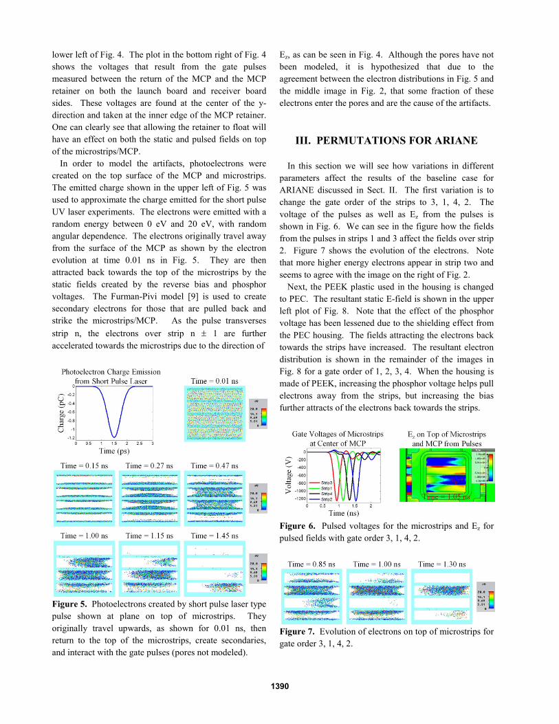
“Streak” artifacts have been observed as the NIF yields have increased and the data provided by framing cameras have been further resolved [2]. Images that illustrate typical artifacts are shown in Fig. 2 for the ARIANE framing camera [2], [3]. In Fig. 2, the image on the left is from an experiment performed on the NIF with a pinhole array. The streak can clearly be seen at the third strip. To record this data the microstrips were pulsed in the order 2, 4, 1, 3 (1 at top, 4 at bottom). The image in the center and on the right are produced from a short pulse UV laser experiment with no pinhole array for gate orders 1, 2, 3, 4, and 3, 1, 4, 2, respectively. A theory was proposed that the origins of these artifacts are due to photoelectrons produced on top of the microstrips/MCP being confined by the static E-fields formed by the DC reverse bias and the phosphor voltages [2]. These electrons then enter the pores and degrade the image. In the remainder of this paper we will discuss EM particle-in-a-cell modeling results from CST Particle Studio for the ARIANE framing camera and a two strip framing camera to further understand the streaks. We will also discuss a technique that can be used to mitigate the streaks by affecting the static E-fields on top of the microstrips/MCP to change electron trajectories [2], [8].
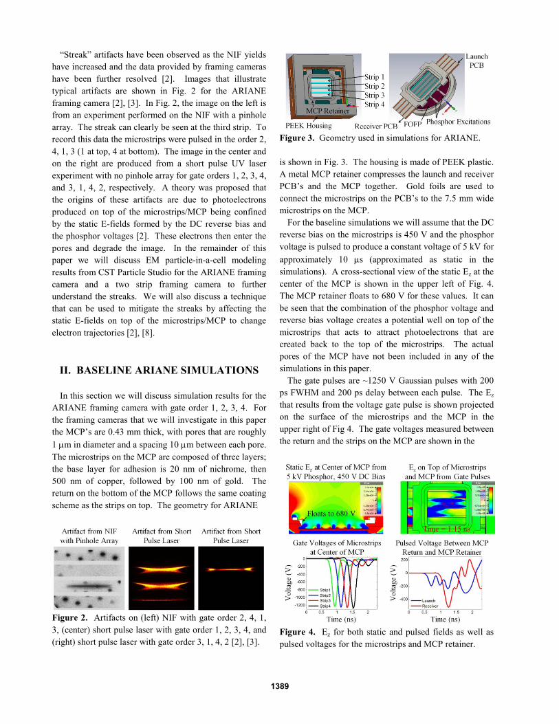
II. BASELINE ARIANE SIMULATIONS In this section we will discuss simulation results for the ARIANE framing camera with gate order 1, 2, 3, 4. For the framing cameras that we will investigate in this paper the MCP’s are 0.43 mm thick, with pores that are roughly 1 µm in diameter and a spacing 10 µm between each pore. The microstrips on the MCP are composed of three layers; the base layer for adhesion is 20 nm of nichrome, then 500 nm of copper, followed by 100 nm of gold. The return on the bottom of the MCP follows the same coating scheme as the strips on top. The geometry for ARIANE
Figure 2. Artifacts on (left) NIF with gate order 2, 4, 1, 3, (center) short pulse laser with gate order 1, 2, 3, 4, and (right) short pulse laser with gate order 3, 1, 4, 2 [2], [3].
Figure 3. Geometry used in simulations for ARIANE. is shown in Fig. 3. The housing is made of PEEK plastic. A metal MCP retainer compresses the launch and receiver PCB’s and the MCP together. Gold foils are used to connect the microstrips on the PCB’s to the 7.5 mm wide microstrips on the MCP. For the baseline simulations we will assume that the DC reverse bias on the microstrips is 450 V and the phosphor voltage is pulsed to produce a constant voltage of 5 kV for approximately 10 µs (approximated as static in the simulations). A cross-sectional view of the static Ez at the center of the MCP is shown in the upper left of Fig. 4. The MCP retainer floats to 680 V for these values. It can be seen that the combination of the phosphor voltage and reverse bias voltage creates a potential well on top of the microstrips that acts to attract photoelectrons that are created back to the top of the microstrips. The actual pores of the MCP have not been included in any of the simulations in this paper.
The gate pulses are ~1250 V Gaussian pulses with 200 ps FWHM and 200 ps delay between each pulse. The Ez that results from the voltage gate pulse is shown projected on the surface of the microstrips and the MCP in the upper right of Fig 4. The gate voltages measured between the return and the strips on the MCP are shown in the
Figure 4. Ez for both static and pulsed fields as well as pulsed voltages for the microstrips and MCP retainer.
1389
lower left of Fig. 4. The plot in the bottom right of Fig. 4 shows the voltages that result from the gate pulses measured between the return of the MCP and the MCP retainer on both the launch board and receiver board sides. These voltages are found at the center of the y-direction and taken at the inner edge of the MCP retainer. One can clearly see that allowing the retainer to float will have an effect on both the static and pulsed fields on top of the microstrips/MCP. In order to model the artifacts, photoelectrons were created on the top surface of the MCP and microstrips. The emitted charge shown in the upper left of Fig. 5 was used to approximate the charge emitted for the short pulse UV laser experiments. The electrons were emitted with a random energy between 0 eV and 20 eV, with random angular dependence. The electrons originally travel away from the surface of the MCP as shown by the electron evolution at time 0.01 ns in Fig. 5. They are then attracted back towards the top of the microstrips by the static fields created by the reverse bias and phosphor voltages. The Furman-Pivi model [9] is used to create secondary electrons for those that are pulled back and strike the microstrips/MCP. As the pulse transverses strip n, the electrons over strip n ± 1 are further accelerated towards the microstrips due to the direction of
Figure 5. Photoelectrons created by short pulse laser type pulse shown at plane on top of microstrips. They originally travel upwards, as shown for 0.01 ns, then return to the top of the microstrips, create secondaries, and interact with the gate pulses (pores not modeled).
Ez, as can be seen in Fig. 4. Although the pores have not been modeled, it is hypothesized that due to the agreement between the electron distributions in Fig. 5 and the middle image in Fig. 2, that some fraction of these electrons enter the pores and are the cause of the artifacts.
III. PERMUTATIONS FOR ARIANE In this section we will see how variations in different parameters affect the results of the baseline case for ARIANE discussed in Sect. II. The first variation is to change the gate order of the strips to 3, 1, 4, 2. The voltage of the pulses as well as Ez from the pulses is shown in Fig. 6. We can see in the figure how the fields from the pulses in strips 1 and 3 affect the fields over strip 2. Figure 7 shows the evolution of the electrons. Note that more higher energy electrons appear in strip two and seems to agree with the image on the right of Fig. 2. Next, the PEEK plastic used in the housing is changed to PEC. The resultant static E-field is shown in the upper left plot of Fig. 8. Note that the effect of the phosphor voltage has been lessened due to the shielding effect from the PEC housing. The fields attracting the electrons back towards the strips have increased. The resultant electron distribution is shown in the remainder of the images in Fig. 8 for a gate order of 1, 2, 3, 4. When the housing is made of PEEK, increasing the phosphor voltage helps pull electrons away from the strips, but increasing the bias further attracts of the electrons back towards the strips.
Figure 6. Pulsed voltages for the microstrips and Ez for pulsed fields with gate order 3, 1, 4, 2.
Figure 7. Evolution of electrons on top of microstrips for gate order 3, 1, 4, 2.
1390
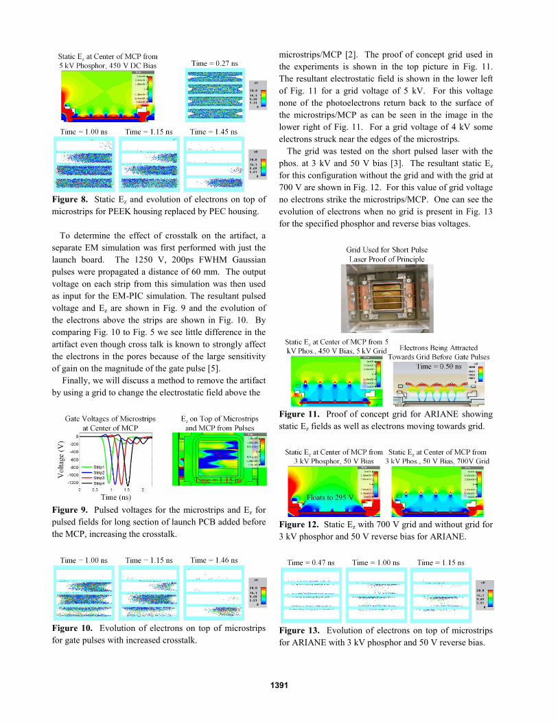
Figure 8. Static Ez and evolution of electrons on top of microstrips for PEEK housing replaced by PEC housing. To determine the effect of crosstalk on the artifact, a separate EM simulation was first performed with just the launch board. The 1250 V, 200ps FWHM Gaussian pulses were propagated a distance of 60 mm. The output voltage on each strip from this simulation was then used as input for the EM-PIC simulation. The resultant pulsed voltage and Ez are shown in Fig. 9 and the evolution of the electrons above the strips are shown in Fig. 10. By comparing Fig. 10 to Fig. 5 we see little difference in the artifact even though cross talk is known to strongly affect the electrons in the pores because of the large sensitivity of gain on the magnitude of the gate pulse [5].
Finally, we will discuss a method to remove the artifact by using a grid to change the electrostatic field above the
Figure 9. Pulsed voltages for the microstrips and Ez for pulsed fields for long section of launch PCB added before the MCP, increasing the crosstalk.
Figure 10. Evolution of electrons on top of microstrips for gate pulses with increased crosstalk.
microstrips/MCP [2]. The proof of concept grid used in the experiments is shown in the top picture in Fig. 11. The resultant electrostatic field is shown in the lower left of Fig. 11 for a grid voltage of 5 kV. For this voltage none of the photoelectrons return back to the surface of the microstrips/MCP as can be seen in the image in the lower right of Fig. 11. For a grid voltage of 4 kV some electrons struck near the edges of the microstrips. The grid was tested on the short pulsed laser with the phos. at 3 kV and 50 V bias [3]. The resultant static Ez for this configuration without the grid and with the grid at 700 V are shown in Fig. 12. For this value of grid voltage no electrons strike the microstrips/MCP. One can see the evolution of electrons when no grid is present in Fig. 13 for the specified phosphor and reverse bias voltages.
Figure 11. Proof of concept grid for ARIANE showing static Ez fields as well as electrons moving towards grid.
Figure 12. Static Ez with 700 V grid and without grid for 3 kV phosphor and 50 V reverse bias for ARIANE.
Figure 13. Evolution of electrons on top of microstrips for ARIANE with 3 kV phosphor and 50 V reverse bias.
1391

IV. TWO STRIP FRAMING CAMERA In this section we discuss results for a two strip framing camera. The geometry is similar to the ARIANE geometry except the housing is made of metal, a metal light shield lays roughly 25 mm above MCP, and the strips are each 15 mm wide. We begin investigating the artifact by assuming 8 kV phosphor, 450 V reverse bias voltage with 1250 V pulses that have 200 ps FWHM. The resultant static and pulsed Ez are shown in the top two images of Fig. 14, while the bottom two plots show the voltages due to the gate pulse at the center of the microstrips and of the MCP retainer. The photoelectron charge originally emitted is the same as that shown in Fig. 5. The evolution of the electrons on top of the microstrips/MCP for these parameters is shown in Fig. 15.
Figure 14. Ez for both static and pulsed fields as well as pulsed voltages for the microstrips and MCP retainer for a two strip gated framing camera.
Figure 15. Evolution of electrons on top of microstrips for two strip framing camera.
We can infer from Fig. 15 that artifacts will once again occur due to the fields that are created above the microstrips/MCP. We can see that higher energy electrons, which are expected to contribute more to the artifacts, occur slightly off the edge of the second microstrip. Once again a grid was used to try to help mitigate the artifact [2], [3]. For this “production” grid, the voltage for the grid is pulled from the phosphor voltage and a voltage divider is used to set the grid voltage [2], [3]. The electrodes for the voltage divider are shown in Fig. 16, but the capacitances and resistances used in the divider were not included in the EM-PIC models. Also visible in Fig. 16 is the bottom part of the PEEK plastic that the voltage divider sits in, not visible is a top PEEK cover. The capacitances, including mutual capacitances, of the electrodes used in the voltage divider were found using the Ansys code MAXWELL3D. A circuit simulation was then performed to choose the capacitors and resistors used to set the grid voltage to 2.8 kV [10]. It was found that the percent difference between measurements and simulations for the grid voltage were less than 6%. The resultant static Ez for the configuration is shown in the right hand side of Fig. 16. Figure 17 shows that most of the electrons are attracted towards the grid, but a small fraction still strike the edges of the microstrips. The final numerical experiment performed was to decrease the value of the reverse bias for the two strip configuration until no electrons strike the microstrips/MCP. Keeping the phosphor and grid voltages fixed, it was found that no electrons struck the microstrips/MCP when the reverse bias was reduced to
Figure 16. Voltage divider and grid for two strip framing camera, modifying the static Ez field.
Figure 17. Most electrons are attracted to the grid, but some still strike microstrips for 450 V reverse bias.
1392

150 V. The resultant static Ez is shown for in Fig. 18 with and without the grid. The evolution of the electrons on top of the microstrips is shown in Fig. 19 when no grid is present.
V. Conclusion
In this paper we have seen how modern computational techniques can be used to help understand a process for how artifacts can be formed for the gated framing cameras that are used at the NIF. We have seen how the static E-fields created by the phosphor voltage and reverse DC bias, as well as the pulsed fields from nearby microstrips effect the artifact. A grid was used to help mitigate the effects of the artifact. It is expected that using the computational tools developed in this paper will be useful to help set voltages or determine their effects on the artifact, rather than relying only on purely empirical techniques. There is still some investigation to be done in the future to further understand all the artifacts seen from NIF data. In some of the artifacts seen on NIF the “streaks” appear narrower then what was shown in the simulations or short pulsed UV laser lab. Simulations varying the energy spectrum of the emitted photoelectrons and duration of emission are currently being performed as well as changing the FWHM of the pulses. It is also anticipated that it will be useful to include several pores in a simulation to show the photoelectrons generated on top of the microstrip/MCP getting pulled into some pores.
Figure 18. Static Ez with and without grid for 8 kV phosphor and 150 V reverse bias for two strip camera.
Figure 19. Evolution of electrons on top of microstrips for two strip with 8 kV phosphor and 150 V reverse bias.
VI. ACKNOWLEDGEMENTS
The authors would like to thank Fred Allen and Brad Petre of LLNL for help with obtaining the correct mechanical schematics needed to input the geometry into CST. We would also like to Monica Garcia for administrative support.
VII. REFERENCES [1] P.M. Bell, D.K. Bradley, J.D. Kilkenny, et al., “Radiation Hardening of Gated X-ray Imagers for the National Ignition Facility,” Rev. Sci. Instrum. 81, 2010, 10E540. [2] Private Communications with J.P. Holder and L.R. Benedetti at LLNL, 2012. [3] L.R. Benedetti et al., “Investigation and suppression of artifacts in X-ray Framing Cameras due to Advance Radiation Incident on Microchannel Plates,” Proc. of SPIE 2013. [4] J.P. Holder, D.R. Hargrove, C.T. Sibernagel, T.S. Perry, D.K. Bradley, and P.M. Bell, “Nanosecond Gating of Microstripline Microchannel Plate Framing Cameras: Characterization and Simulation,” 15th Topical Conf. High Temp. Plasma Diag., 2004. [5] L.R. Benedetti, et al., “Crosstalk in X-ray Framing Cameras: Effect on Voltage, Gain, and Timing,” Rev. Sci. Instrum. 83, 10E135, 2012. [6] M.J. Ayers, et al., “Design and Implementation of Magnification Framing Camera for NIF ARIANE Light,” Proc. SPIE, 2012. [7] J.A. Oertel, et al., “Gated X-ray Detector for the National Ignition Facility,” Rev. Sci. Inst. 77, 10E308, 2006. [8] R.C. Taylor, M.C. Hettrick, R.F. Malina, “Maximizing the Quantum Efficiency of Microchannel Plate Detectors: The Collection of Photoelectrons from the Interchannel Web using an Electric Field, “Rev. Sci. Inst. 54(2), 1983. [9] M.A. Furman, M.T.F. Pivi, “Probabilistic Model for the Simulation of Secondary Electron Emission,” Phys. Rev. Accel. And Beams Vol. 5, 124404, 2002. [10] C.S. Anderson, L.R. Benedetti, C.G. Brown, J.P. Holder, M.P. Perkins, K.W. Piston, “P-Spice Modeling of Attractor Grid Voltage for Implementation in NIF GXD Framing Cameras,” LLNL-TR 2013.
1393