
Compound Semiconductors: Process Flow, Process Integration ...csmantech.org/OldSite/Conference...
45
1 4/28/2010 Ravi Ramanathan Skyworks Solutions, Inc. Compound Semiconductors: Process Flow, Process Integration, Devices and Testing May 2010
Transcript of Compound Semiconductors: Process Flow, Process Integration ...csmantech.org/OldSite/Conference...

1 4/28/2010
Ravi RamanathanSkyworks Solutions, Inc.
Compound Semiconductors:Process Flow, Process Integration,
Devices and Testing
May 2010
2 4/28/2010
Prelude
• Compound Semiconductor Market Value• An Example: Process Technologies in a Radio• Industry Trend in Power Amplifier/Front-end Modules• Multi-Mode, Multi-Band Radio• Process Technology Evolution• Widely Used Compound Semiconductor Devices• Heterostructures

3 4/28/2010
Compound Semiconductor Market Value
GaN LED: http://www.lbl.gov/Science-Articles/Archive/assets/images/2002/Dec-17-2002/indium_LED.jpgLaser Diode: http://www.aeropause.com/archives/Blu-ray-cover_plat.jpg
Mobile Internet
Laser Diodes
Smart Grid HB-LED/SSL
3G, 4G Data Cards
http://www.bccresearch.com/report/SMC032C.html
CAGR of 10%-18%Embedded Wireless Platforms
4 4/28/2010
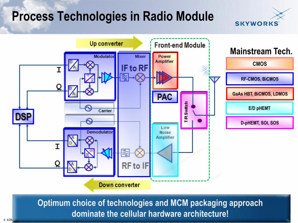
CMOS
RF-CMOS, BiCMOS
GaAs HBT, BiCMOS, LDMOS
E/D pHEMT
D-pHEMT, SOI, SOS
Mainstream Tech.
Optimum choice of technologies and MCM packaging approach dominate the cellular hardware architecture!
Process Technologies in Radio Module
5 4/28/2010
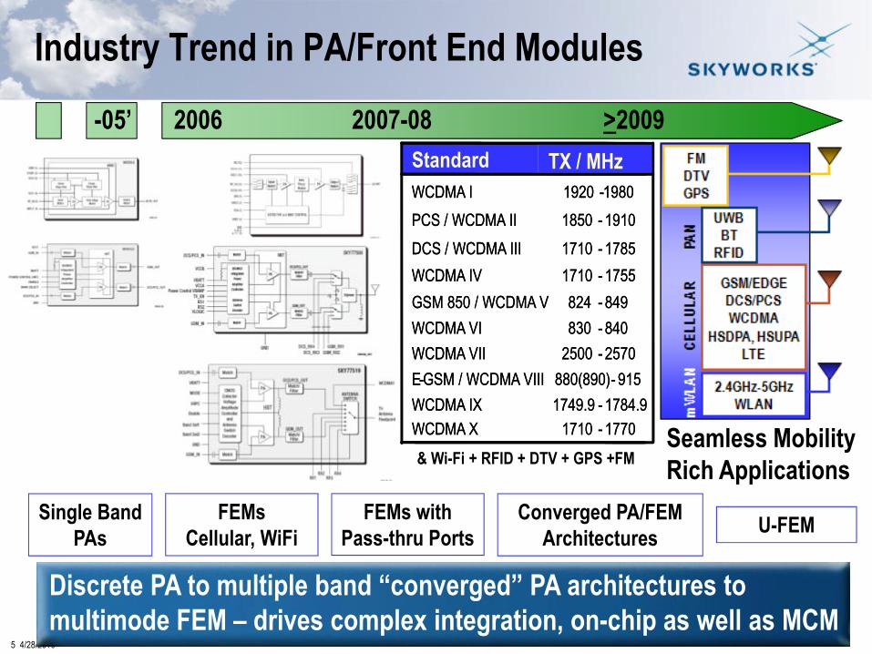
Industry Trend in PA/Front End Modules
Discrete PA to multiple band “converged” PA architectures to multimode FEM – drives complex integration, on-chip as well as MCM
2007-08 >2009-05’ 2006
1710 - 1770WCDMA X1749.9 - 1784.9WCDMA IX880(890) - 915E-GSM / WCDMA VIII2500 - 2570WCDMA VII830 - 840WCDMA VI824 - 849GSM 850 / WCDMA V
1710 - 1755WCDMA IV1710 - 1785DCS / WCDMA III1850 - 1910PCS / WCDMA II1920 -1980WCDMA I
TX / MHzStandard
1710 - 1770WCDMA X1749.9 - 1784.9WCDMA IX880(890) - 915E-GSM / WCDMA VIII2500 - 2570WCDMA VII830 - 840WCDMA VI824 - 849GSM 850 / WCDMA V
1710 - 1755WCDMA IV1710 - 1785DCS / WCDMA III1850 - 1910PCS / WCDMA II1920 -1980WCDMA I
TX / MHz
& Wi-Fi + RFID + DTV + GPS +FM
Single Band PAs
FEMsCellular, WiFi
FEMs withPass-thru Ports
Converged PA/FEM Architectures U-FEM
Seamless MobilityRich Applications

6 4/28/2010
• Radios are becoming complex with the introduction of multiple modes and multiple bands in a single package (SiP).
• Compound Semiconductors dominate the power amplifier, front-end modules and switch applications.– Power amplifiers and front-end modules are fabricated using heterojunction
bipolar transistors• N. Sokal, RF Power Amplifiers - Classes A Through F (Overview), IEEE, 1996.• S.C. Cripps, RF Power Amplifiers for Wireless Communications, Artech House, Book
publication.– Antenna switch modules (ASMs) and diversity switches are fabricated using
depletion mode pHEMT and J-pHEMT devices, low noise amplifiers using E/D pHEMT devices.
• H. Tosaka et al., An Antenna Switch MMIC Using E/D Mode p-HEMT for GSM/DCS/PCS/WCDMA Bands Application, 2003 IEEE Radio Frequency Integrated Circuits Symposium, page 519.
• S. Tamari et al., Recessed JPHEMT Technology for Low Distortion and Low Insertion Loss Switch, CS MANTECH Conference, May 2009, Tampa, Florida, USA
Multi Mode and Multi Band Radio
7 4/28/2010
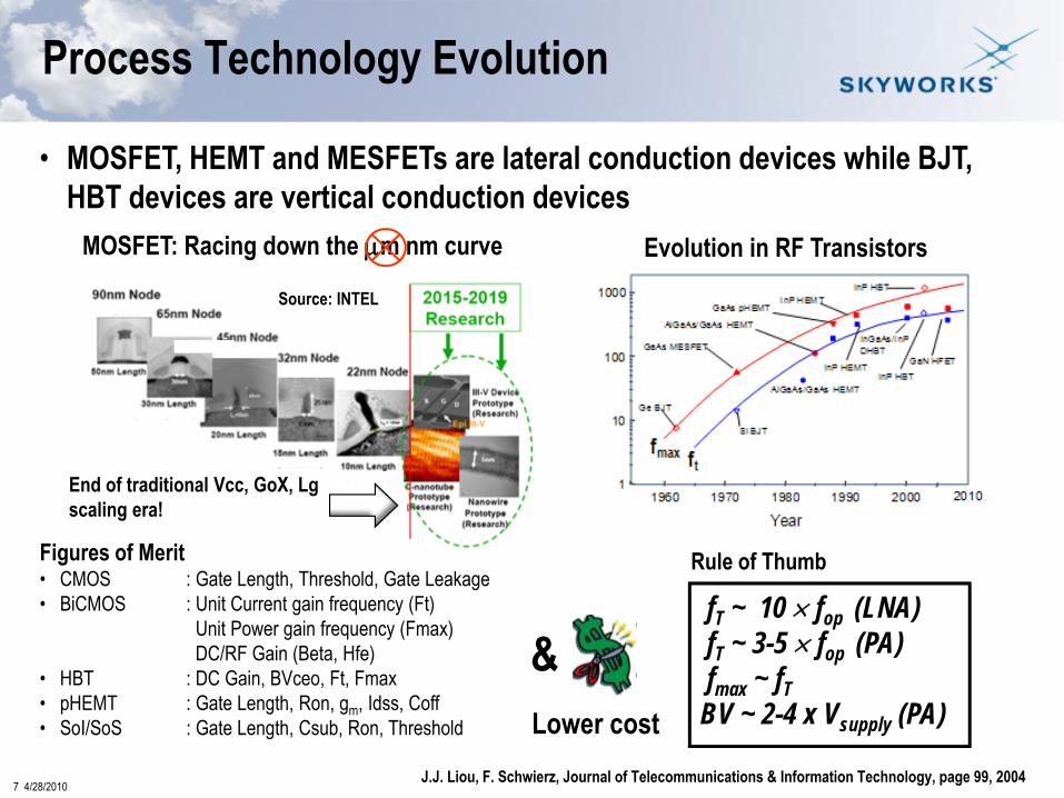
• MOSFET, HEMT and MESFETs are lateral conduction devices while BJT, HBT devices are vertical conduction devices
fT ~ 10 × fop (LNA)fT ~ 3-5 × fop (PA)fmax ~ fTBV ~ 2-4 x Vsupply (PA)
Rule of Thumb
Source: INTEL
MOSFET: Racing down the μm nm curve
Figures of Merit• CMOS : Gate Length, Threshold, Gate Leakage• BiCMOS : Unit Current gain frequency (Ft)
Unit Power gain frequency (Fmax) DC/RF Gain (Beta, Hfe)
• HBT : DC Gain, BVceo, Ft, Fmax• pHEMT : Gate Length, Ron, gm, Idss, Coff• SoI/SoS : Gate Length, Csub, Ron, Threshold
Evolution in RF Transistors
&Lower cost
Process Technology Evolution
End of traditional Vcc, GoX, Lg scaling era!
J.J. Liou, F. Schwierz, Journal of Telecommunications & Information Technology, page 99, 2004

8 4/28/2010
Compound Semiconductor Devices
• Heterojunction Bipolar Transistors– HBT used for power amplification
• pHEMT (Pseudomorphic High Electron Mobility Transistors)– Used as diversity switches, antenna switch module, low noise amplifier,
mmWave amplifiers
• BiFET (Integration of Heterojunction Bipolar and Metal-Semiconductor Field Effect Transistors)– HBT used for power amplification– FET used in the bias circuit and as a “switch”
• BiHEMT (Integration of Heterojunction Bipolar and High Electron Mobility Transistors)– HBT used for power amplification– HEMT used in the bias circuit as well as a “switch” to turn some HBT arrays
“ON” and “OFF”
9 4/28/2010
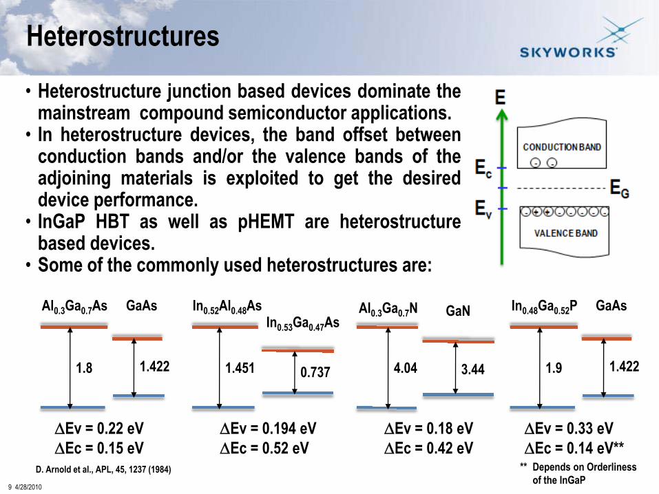
Heterostructures
• Heterostructure junction based devices dominate themainstream compound semiconductor applications.
• In heterostructure devices, the band offset betweenconduction bands and/or the valence bands of theadjoining materials is exploited to get the desireddevice performance.
• InGaP HBT as well as pHEMT are heterostructurebased devices.
• Some of the commonly used heterostructures are:
1.8
Al0.3Ga0.7As
1.422
GaAs
ΔEv = 0.22 eVΔEc = 0.15 eV
D. Arnold et al., APL, 45, 1237 (1984)
1.451
In0.52Al0.48As
0.737
ΔEv = 0.194 eVΔEc = 0.52 eV
In0.53Ga0.47As
1.9
In0.48Ga0.52P
1.422
GaAs
ΔEv = 0.33 eVΔEc = 0.14 eV**
4.04 3.44
ΔEv = 0.18 eVΔEc = 0.42 eV
GaNAl0.3Ga0.7N
** Depends on Orderliness of the InGaP

10 4/28/2010
Organization of Process Flows
• Front-end of Line Device Processing– HBT– pHEMT– BiFET vs. BiHEMT– Diodes (Schottky, Junction Diodes)
• Back-end of Line Interconnect Processing– General Process Flow– Passives
• Resistors• Capacitors• Inductors• Bondpads
• Backside Process Flow (through Wafer Via)
11 4/28/2010
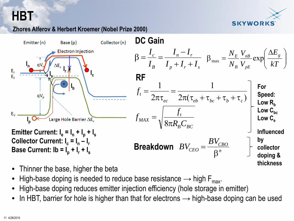
HBT
• Thinner the base, higher the beta • High-base doping is needed to reduce base resistance → high Fmax.• High-base doping reduces emitter injection efficiency (hole storage in emitter)• In HBT, barrier for hole is higher than that for electrons → high-base doping can be used
Zhores Alferov & Herbert Kroemer (Nobel Prize 2000)
srp
rn
B
c
IIIII
II
++−
==β
DC Gain
InIc
Ir
Ib
*
Ip
Is
Emitter Current: Ie = In + Ip + IsCollector Current: Ic = In – IrBase Current: Ib = Ip + Ir + Is
⎟⎟⎠
⎞⎜⎜⎝
⎛ Δ=β
kTE
VV
NN g
pE
nB
B
E expmax
RF
)21
21
cbbcebectf τ+τ+τ+π(τ
=πτ
=
BCB
tMAX CR
ffπ
=8
ForSpeed:Low RbLow CbcLow Ce
nCBO
CEOBVBVβ
=BreakdownInfluenced by collector doping & thickness

12 4/28/2010
InGaP/GaAs HBT
Key Features:(i) Very low output conductance (high base doping), (ii) Fairly constant gain as function of Ib, (iii) Low turn on voltage, (iv) High breakdown voltage
Emitter contact: Ti/Pt (n-type ohmic contact)Base contact: Pt/Ti (p-type ohmic contact)Collector contact: AuGeNi (n-type alloyed contact)
Careful design of epitaxial layer structures as well as optimized device layout geometry are critical to achieve consistent device and circuit performance.
InGaP (Emitter)GaAs (Base)
• HBT devices must be protected with proper ballasting scheme to ensure thermal stability
Base Ballasting
Emitter Ballasting
Rbb
Reb Rbb = β Reb
13 4/28/2010
Layout
Establishing “Statistical Process Control” at device fabrication steps is vital to achieve high yield and consistent performance.
Typical Process Flow Device
TEM
InGaP
Emitter Mesa
InGaAs Cap
Contact Metal TEMof
Emitter of
HBT structure
MOCVD HBTWafers
MOCVD HBTWafers
Emitter ContactPhoto & Metal
Emitter ContactPhoto & Metal E/B/C Nitride
Photo & Etch
E/B/C NitridePhoto & Etch
Emitter MesaPhoto & Etch
Emitter MesaPhoto & Etch Collector Photo
Etch & Metal
Collector PhotoEtch & Metal
Base PedestalPhoto & Etch
Base PedestalPhoto & Etch
IsolationPhoto & Implant
IsolationPhoto & Implant
Base PhotoEtch & Metal
Base PhotoEtch & Metal
RTP AlloyRTP Alloy
Nitride Deposition
Nitride DepositionMOCVD HBT
Wafers
MOCVD HBTWafers
Emitter ContactPhoto & Metal
Ti/PtEmitter Contact E/B/C Nitride
Photo & Etch
Contact ViasE/B/C
Emitter MesaPhoto & Etch
Emitter MesaDry or Dry/Wet etch Collector Photo
Etch & Metal
CollectorDefinition (Wet Etch)
Base PedestalPhoto & Etch
Base PedestalDry or Wet etch
IsolationPhoto & Implant
Implant Isolation(He++)
Base PhotoEtch & Metal
Base ContactDefinition
RTP AlloyAu-Ge-Ni
Alloy Process
Nitride Deposition
Nitride Passivation
HBT Fabrication – Carving the device
Epitaxial Material
14 4/28/2010
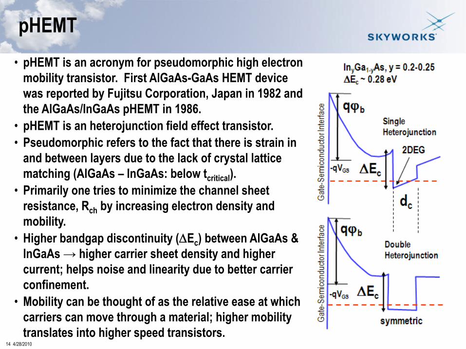
• pHEMT is an acronym for pseudomorphic high electron mobility transistor. First AlGaAs-GaAs HEMT device was reported by Fujitsu Corporation, Japan in 1982 and the AlGaAs/InGaAs pHEMT in 1986.
• pHEMT is an heterojunction field effect transistor. • Pseudomorphic refers to the fact that there is strain in
and between layers due to the lack of crystal lattice matching (AlGaAs – InGaAs: below tcritical).
• Primarily one tries to minimize the channel sheet resistance, Rch by increasing electron density and mobility.
• Higher bandgap discontinuity (ΔEc) between AlGaAs & InGaAs → higher carrier sheet density and higher current; helps noise and linearity due to better carrier confinement.
• Mobility can be thought of as the relative ease at which carriers can move through a material; higher mobility translates into higher speed transistors.
pHEMT

15 4/28/2010
Doped AlGaAs layer on top of an undoped InGaAs layer supplies electrons to the InGaAs channel layer
Flow of electrons in the InGaAs layer with no scattering (undoped channel). This also provides better noise figure.
Von Helmut Brech, 1998 Doctoral Dissertation, Optimization of GaAs based HEMT by Numerical Simulations, Vienna Univ of Technology, Vienna, Austria
pHEMT: Epitaxial Layer Construction
Spacing between AlGaAs and InGaAs channel is adjusted to achieve desired breakdown characteristics and separates the 2DEG from any ionized donors from n+ active.
10-20 periods of AlGaAs/GaAs super lattices grown on GaAs to inhibit substrate conductionBottom layer heterojunction (double heterojunction pHEMT)
InGaP or AlAs etch stops
More than 50+ layers are grown by MBE.
Real Bandgap Engineering…
16 4/28/2010
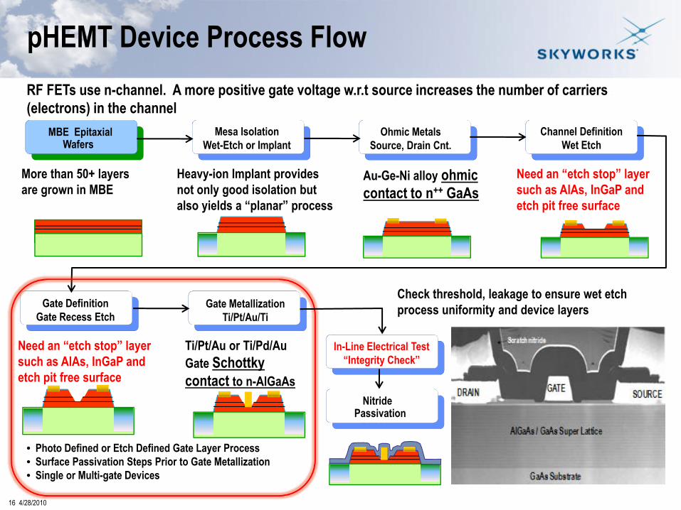
pHEMT Device Process FlowRF FETs use n-channel. A more positive gate voltage w.r.t source increases the number of carriers (electrons) in the channel
MOCVD HBTMOCVD HBTWafersMOCVD HBTMBE EpitaxialWafers Emitter Contact
Photo & MetalEmitter ContactPhoto & MetalEmitter Contact
Photo & MetalMesa Isolation
Wet-Etch or Implant Emitter MesaPhoto & Etch
Emitter MesaPhoto & EtchEmitter Mesa
Photo & EtchOhmic Metals
Source, Drain Cnt. Base PedestalPhoto & Etch
Base PedestalPhoto & EtchBase Pedestal
Photo & EtchChannel Definition
Wet Etch
IsolationPhoto & Implant
IsolationPhoto & ImplantIsolation
Photo & ImplantGate Definition
Gate Recess Etch Base PhotoEtch & MetalBase Photo
Etch & MetalBase PhotoEtch & Metal
Gate MetallizationTi/Pt/Au/Ti
Nitride DepositionNitride
DepositionNitride DepositionNitride
Passivation
Nitride DepositionNitride
DepositionNitride Deposition
In-Line Electrical Test“Integrity Check”
More than 50+ layers are grown in MBE
Heavy-ion Implant provides not only good isolation but also yields a “planar” process
Au-Ge-Ni alloy ohmic contact to n++ GaAs
Need an “etch stop” layer such as AlAs, InGaP and etch pit free surface
• Photo Defined or Etch Defined Gate Layer Process• Surface Passivation Steps Prior to Gate Metallization• Single or Multi-gate Devices
Need an “etch stop” layer such as AlAs, InGaP and etch pit free surface
Ti/Pt/Au or Ti/Pd/AuGate Schottky contact to n-AlGaAs
Check threshold, leakage to ensure wet etch process uniformity and device layers
17 4/28/2010
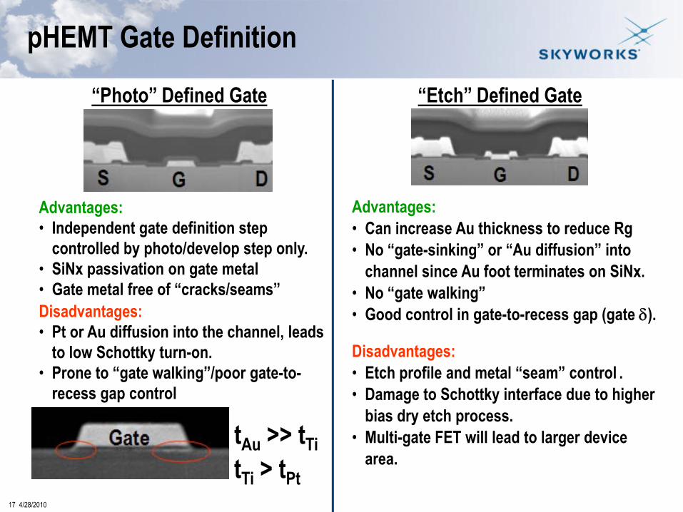
“Photo” Defined Gate
Advantages:• Independent gate definition step
controlled by photo/develop step only.• SiNx passivation on gate metal• Gate metal free of “cracks/seams”Disadvantages:• Pt or Au diffusion into the channel, leads
to low Schottky turn-on.• Prone to “gate walking”/poor gate-to-
recess gap control
tAu >> tTitTi > tPt
“Etch” Defined Gate
Advantages:• Can increase Au thickness to reduce Rg• No “gate-sinking” or “Au diffusion” into
channel since Au foot terminates on SiNx.• No “gate walking”• Good control in gate-to-recess gap (gate δ).
Disadvantages:• Etch profile and metal “seam” control .• Damage to Schottky interface due to higher
bias dry etch process.• Multi-gate FET will lead to larger device
area.
pHEMT Gate Definition

18 4/28/2010
Typical Device Characteristics of D-mode and E-mode pHEMT
Depletion/Enhancement Mode pHEMT
• In a typical depletion mode pHEMT, the gate must be made negative to turn off the “normally on” device.
• In contrast, an enhancement mode device is “normally off” at Vg = 0 and requires that the gate be made more positive than the source for normal operation.
• Therefore a negative power supply voltage is not required for an enhancement mode device.
• Biasing an enhancement mode pHEMT is much like biasing the typical bipolar junction transistor
19 4/28/2010
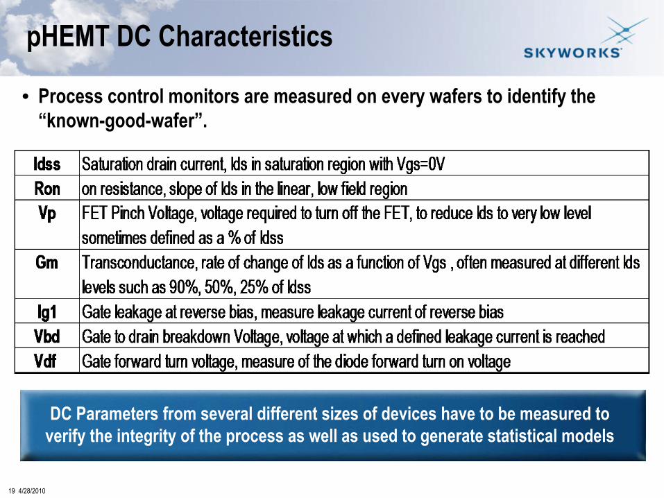
pHEMT DC Characteristics
DC Parameters from several different sizes of devices have to be measured to verify the integrity of the process as well as used to generate statistical models
• Process control monitors are measured on every wafers to identify the “known-good-wafer”.

20 4/28/2010
pHEMT RF Characteristics
• For multi-gate, multi-pole/multi-throw switches, it is vital to monitor the RF characteristics of the switch to identify “known-good-die”.
21 4/28/2010
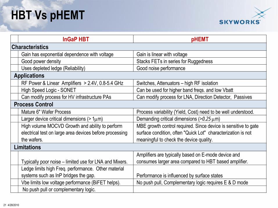
HBT Vs pHEMT
InGaP HBT pHEMT
Gain has exponential dependence with voltage Gain is linear with voltageGood power density Stacks FETs in series for RuggednessUses depleted ledge (Reliability) Good noise performance
RF Power & Linear Amplifiers > 2.4V, 0.8-5.4 GHz Switches, Attenuators – high RF isolationHigh Speed Logic - SONET Can be used for higher band freqs. and low Vbatt Can modify process for HV infrastructure PAs Can modify process for LNA, Direction Detector, Passives
Mature 6" Wafer Process Process variability (Yield, Cost) need to be well understood.Larger device critical dimensions (> 1μm) Demanding critical dimensions (>0.25μm)High volume MOCVD Growth and ability to perform electrical test on large area devices before processing the wafers.
MBE growth control required. Since device is sensitive to gate surface condition, often "Quick Lot" characterization is not meaningful to check the device quality.
Typically poor noise – limited use for LNA and Mixers.Amplifiers are typically based on E-mode device and consumes larger area compared to HBT based amplifier.
Ledge limits high Freq. performance. Other material systems such as InP bridges the gap. Performance is influenced by surface statesVbe limits low voltage performance (BiFET helps). No push pull, Complementary logic requires E & D mode No push pull or complementary logic.
Characteristics
Applications
Process Control
Limitations

22 4/28/2010
• PIN-FET: Integration of P-I-N diode and MESFET 1983• BiFET: HBT Integration with Ion-implanted J-FET (National) 1983• Monolithic Integration of Laser Diodes and HBT 1984• BiFET: FET Integrated into Collector of HBT (Single Growth) 1989• BiHEMT: HEMT Integration with HBT (Re-growth, Selective MBE) 1991, 1995• BiFET: FET Integrated into Emitter of HBT (Single Growth) 1992
• BiFET-based Products – Skyworks, Anadigics 2005
In many cases, FET and/or HBT performance is compromised due to limitations in epitaxial profile and/or process complexities.
Incorporation of Simple MESFET Layer Scheme, in the Emitter Stack of HBT
Incorporation of HFET or pHEMT Layer Schemes, underneath the Collector
Monolithic Integration in GaAs - History
23 4/28/2010
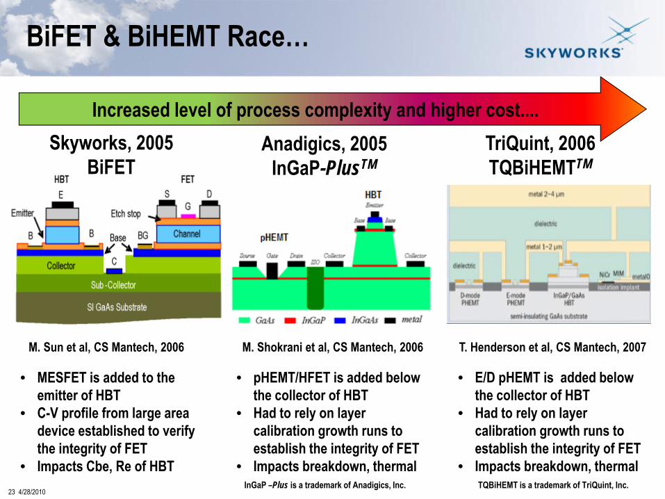
BiFET & BiHEMT Race…
Increased level of process complexity and higher cost....Skyworks, 2005
BiFETAnadigics, 2005
InGaP-PlusTMTriQuint, 2006TQBiHEMTTM
M. Shokrani et al, CS Mantech, 2006M. Sun et al, CS Mantech, 2006 T. Henderson et al, CS Mantech, 2007
• MESFET is added to the emitter of HBT
• C-V profile from large area device established to verify the integrity of FET
• Impacts Cbe, Re of HBT
• pHEMT/HFET is added below the collector of HBT
• Had to rely on layer calibration growth runs to establish the integrity of FET
• Impacts breakdown, thermal
• E/D pHEMT is added below the collector of HBT
• Had to rely on layer calibration growth runs to establish the integrity of FET
• Impacts breakdown, thermalInGaP –Plus is a trademark of Anadigics, Inc. TQBiHEMT is a trademark of TriQuint, Inc.
24 4/28/2010
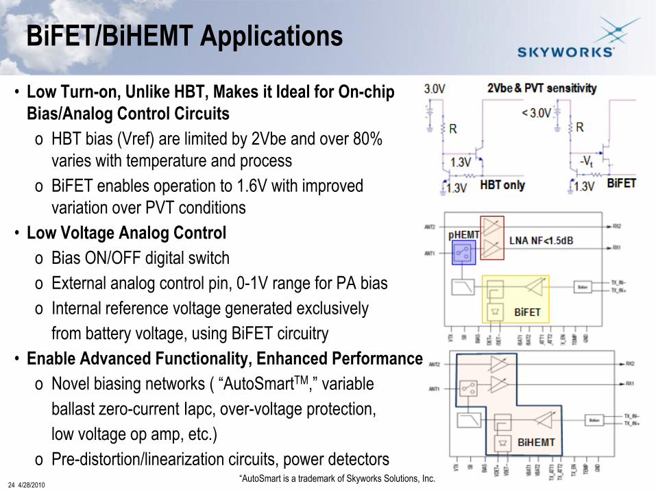
• Low Turn-on, Unlike HBT, Makes it Ideal for On-chip Bias/Analog Control Circuitso HBT bias (Vref) are limited by 2Vbe and over 80%
varies with temperature and processo BiFET enables operation to 1.6V with improved
variation over PVT conditions • Low Voltage Analog Control
o Bias ON/OFF digital switcho External analog control pin, 0-1V range for PA biaso Internal reference voltage generated exclusively
from battery voltage, using BiFET circuitry• Enable Advanced Functionality, Enhanced Performance
o Novel biasing networks ( “AutoSmartTM,” variable ballast zero-current Iapc, over-voltage protection, low voltage op amp, etc.)
o Pre-distortion/linearization circuits, power detectors
BiFET/BiHEMT Applications
“AutoSmart is a trademark of Skyworks Solutions, Inc.

25 4/28/2010
Process Flow for BiFET/BiHEMT
MOCVD HBTWafers
MOCVD HBTWafersMOCVD HBT
Wafers
MOCVD BiFET/BiHEMT Wafer
Emitter ContactPhoto & Metal
Emitter ContactPhoto & MetalEmitter Contact
Photo & MetalEmitter Contact
Emitter MesaPhoto & Etch
Emitter MesaPhoto & EtchEmitter Mesa
Photo & Etch
Emitter MesaDry or Dry/Wet Etch
Collector PhotoEtch & Metal
Collector PhotoEtch & MetalCollector Photo
Etch & Metal
CollectorDefinition
Base PedestalPhoto & Etch
Base PedestalPhoto & EtchBase Pedestal
Photo & Etch
Base PedestalDry or Wet Etch
IsolationPhoto & Implant
IsolationPhoto & ImplantIsolation
Photo & Implant
Implant Isolation(He++)
Base PhotoEtch & Metal
Base PhotoEtch & MetalBase Photo
Etch & Metal
Base ContactDefinition
RTP AlloyRTP AlloyRTP AlloyAu-Ge-NiAlloy Process
Nitride Deposition
Nitride DepositionNitride
Deposition
Nitride Passivation & Vias
Emitter ContactPhoto & Metal
Emitter ContactPhoto & MetalEmitter Contact
Photo & Metal
Channel Mask andWet Etch Process
Emitter ContactPhoto & Metal
Emitter ContactPhoto & MetalEmitter Contact
Photo & Metal
Gate Mask andMetallization
IsolationPhoto & Implant
IsolationPhoto & ImplantIsolation
Photo & Implant
FET ISOLATION(Shared Process)
Emitter ContactPhoto & Metal
Emitter ContactPhoto & MetalEmitter Contact
Photo & Metal
Channel Mask andWet Etch Process
Emitter ContactPhoto & Metal
Emitter ContactPhoto & MetalEmitter Contact
Photo & Metal
Gate Mask andMetallization
BiFET BiHEMT
Emitt
erBa
seCo
llect
or
TOPOLOGY
Challenging to define 0.5μm or sub 0.5μm gates. Requires large spacing between pHEMT and HBT to avoid topology depending processing issues.

26 4/28/2010
BiFET/BiHEMT – Integration Challenges
5 mA/mm and 50 mV for every 10A shift in etch-stop thickness
3 mA/mm and 30 mV for every 10A shift in GaAs thickness80% change in Idss and 30% change in Vp for every 10% shift in channel doping.
• Influence of Epitaxial Layers (Design of Experiments to Correlate Epi Material Characterization Parameters and End-of-Line Device Parameters)
• Influence of Process Conditions― Layout and wet-process optimizationGalvanic corrosion in gate periphery― Nitride vs. photo-defined gate Gate-length control― Surface-passivation step Improved Schottky interface― Gate-placement in HBT flow Thermal stability and Idss/Vt drift
Multitude of “Variables” Can Impact FET Performance and BiFET Yield
0
100
80
60
40
20
0
100
80
60
40
20
0
100
80
60
40
20
0
100
80
60
40
20
Lg
Channel
27 4/28/2010
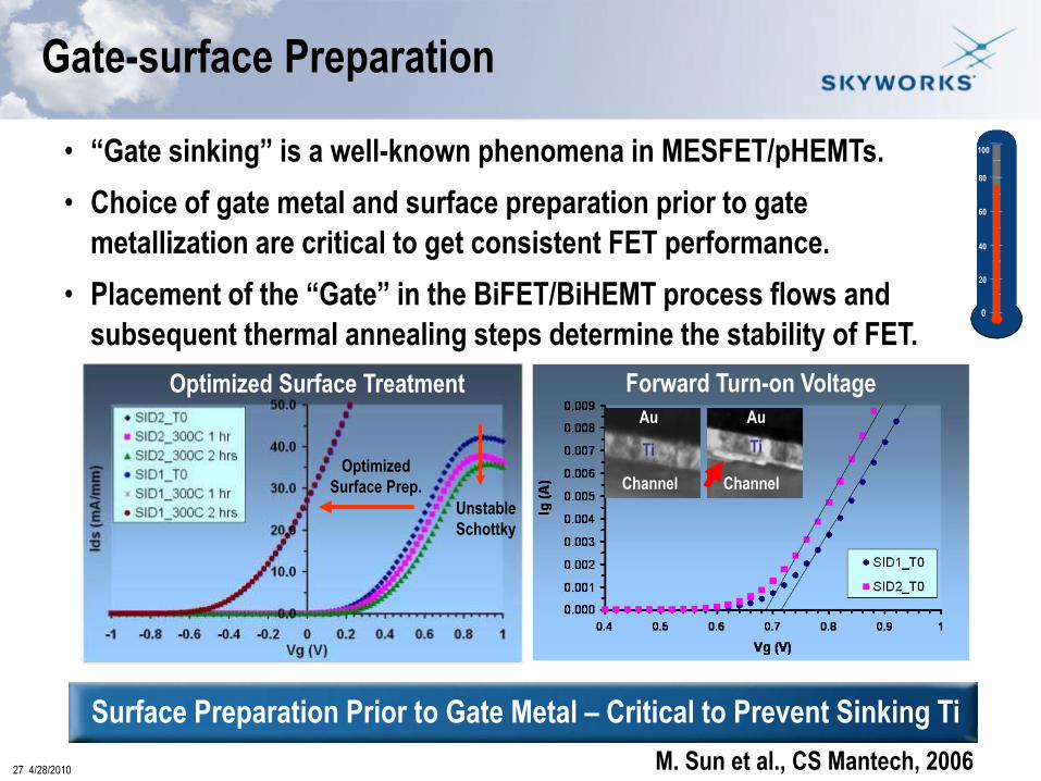
Surface Preparation Prior to Gate Metal – Critical to Prevent Sinking Ti
Optimized Surface Prep.
UnstableSchottky
Optimized Surface Treatment
• “Gate sinking” is a well-known phenomena in MESFET/pHEMTs.• Choice of gate metal and surface preparation prior to gate
metallization are critical to get consistent FET performance.• Placement of the “Gate” in the BiFET/BiHEMT process flows and
subsequent thermal annealing steps determine the stability of FET.Forward Turn-on Voltage
Channel Channel
Ti TiAuAu
Gate-surface Preparation
M. Sun et al., CS Mantech, 2006
0
100
80
60
40
20
0
100
80
60
40
20

28 4/28/2010
0
0.2
0.4
0.6
0.8
1
1.2
Design Flexibility/TTM
Inter-channel Isolation, Noise
Extendibility to Complex Tx/Radio
Supply Chain Complexity
Yield & Integration Risk
Capability to Multi-sourcing
IP Re-use Option
Reliability
Size (Form-Factor)
Fabrication Cost (Yield)
On-chip Integration vs. MCM
Trade-offs have to be considered in choosing a process technology and integration scheme.
MCM: Multi-Chip Module

29 4/28/2010
• Backend of line can be common to both pHEMT and HBT devices.• Processing steps that define resistors, capacitors, inductors and interconnects.• Devices are finally protected by thick silicon nitride and thick polymer layers.• Plated Au interconnects are used when thick metals (>2μm) are desired.
Nitride Via Opening
Via Definition
Thin FilmResistor
Metal 1(Ti/Au/Ti)
MIM NitrideDeposition
Inter LevelDielectric (ILD)
Metal-2(Ti/Au/Ti)
Polymer ScratchProtection (Optional)
Nitride Overcoat
Nitride Etch(Bondpad Opening)
DC/RFParametric
Layout
Scratch protection improves die integrity against scratches as
well as moisture protection.
Passives and Backend of Line
Lift-Off or Dry Etch
Evaporation/Plating
PE-CVD
O2 or O2+CF4Dry Etch
Polyimide or Nitride or BCB
Evaporation orElectro-Plating
PE-CVD
BCB/PBO/Poly
CF4 Plasma Etch
Additional metal layers require additional ILD layers and metallization steps.

30 4/28/2010
• In III-V compound semiconductor technologies, MIM consists of Au metal layers with SiNx dielectric layer and the cap densities range from 0.25 – 1.5 fF/μm2 (single or stacked).
• Plasma enhance CVD technique is used to deposit pin-hole free SiNx dielectric layer.• Capacitors are constructed typically between Metal-1 and Metal-2.• Low leakage, low voltage coefficient (VC) and temperature coefficient (TC) of capacitance,
high-breakdown voltage and higher MTTF are desirable.
Passives: Capacitor
dAC dielectricε
=
LCfR π2
1=
CL
RRCfRXQ
R
c 12
1===
π
Higher QAu/Ti Bottom Plate
Ti/Au/Ti
SiNx
MIM ( SiNx < 500A)
Top plateILD
Au/Ti Bottom Plate
Ti/Au/Ti
MIM (SiNx > 500 A)
SiNx
ILD

31 4/28/2010
• Q-factor of an inductor describes how good an inductor can work as an energy-storage element. In the ideal case, inductance is pure energy-storage element (Q approaches infinity), while in reality, parasitic resistance and capacitance reduce Q. Self-resonant frequency fSR marks the point where the inductor turns to capacitive.
• Solenoid and spiral inductors are popular in GaAs technology. • In Si technologies, techniques to minimize eddy current loss due to
substrate coupling are critical to achieve reasonable Q-values.Patterned Ground Shield Inductor on Deep Trench
Oxide FilledTrenches underneathInductors
Variable Line Width
Shielding
Inductor
Passives: Inductor
Design of Components and Circuits Underneath Integrated InductorsFrank Zhang, IEEE JOURNAL OF SOLID-STATE CIRCUITS, VOL. 41, NO. 10, October 2006
LCfR π2
1=
CL
RRLf
RXQ RL 12
===π
Coupling Effect of On-Chip Inductor with Variable Metal Width, Heng-Ming Hsu, IEEE MICROWAVE AND WIRELESS COMPONENTS LETTERS, VOL. 17, NO. 7, JULY 2007
32 4/28/2010
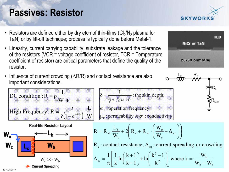
Passives: Resistor
NiCr or TaN
ILD
20-50 ohms/sq
• Resistors are defined either by dry etch of thin-films (Cl2/N2 plasma for TaN) or by lift-off technique; process is typically done before Metal-1.
• Linearity, current carrying capability, substrate leakage and the tolerance of the resistors (VCR = voltage coefficient of resistor, TCR = Temperature coefficient of resistor) are critical parameters that define the quality of the resistor.
• Influence of current crowding (ΔR/R) and contact resistance are also important considerations.
( ) WL
e1δρR:FrequencyHigh
tWLρR :condition DC
t/δ ⋅−
=
⋅=
− tyconductivi : &typermeabili:μfrequency;operation:ω
depth;skinthe:1δ
0
0
0
σ
σμπ f=
cb
b2
2
sq
sqc
sqc
0shc
b
bsh
WWWk where
k1kln
1k1kln
k1
π1Δ
crowdingorspreadingcurrent:Δ ,resistancecontact:R
ΔWWRR2
WLRR
−=⎥
⎦
⎤⎢⎣
⎡⎟⎟⎠
⎞⎜⎜⎝
⎛ −+⎟
⎠⎞
⎜⎝⎛
−+
=
⎟⎟⎠
⎞⎜⎜⎝
⎛⎟⎟⎠
⎞⎜⎜⎝
⎛+⋅++=
bc WW >>Current Spreading
Real-life Resistor Layout
33 4/28/2010
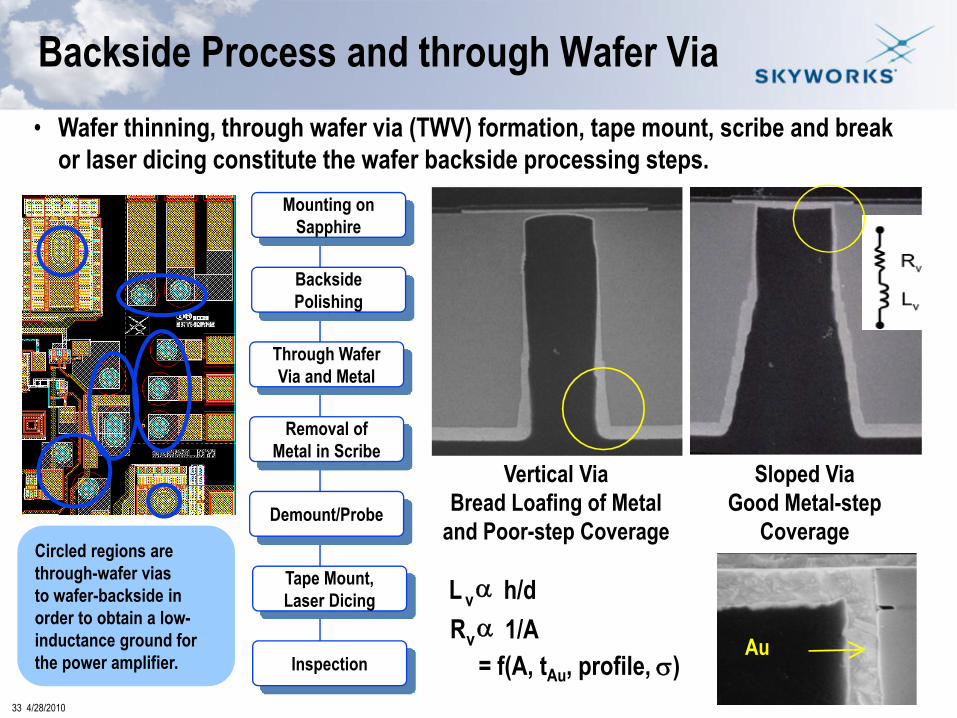
• Wafer thinning, through wafer via (TWV) formation, tape mount, scribe and break or laser dicing constitute the wafer backside processing steps.
Removal ofMetal in Scribe
Mounting onSapphire
BacksidePolishing
Through WaferVia and Metal
Demount/Probe
Tape Mount,Laser Dicing
Inspection
Circled regions are through-wafer viasto wafer-backside in order to obtain a low-inductance ground for the power amplifier.
Backside Process and through Wafer Via
Au
Vertical ViaBread Loafing of Metal
and Poor-step Coverage
Sloped ViaGood Metal-step
Coverage
L vα h/dRvα 1/A
= f(A, tAu, profile, σ)
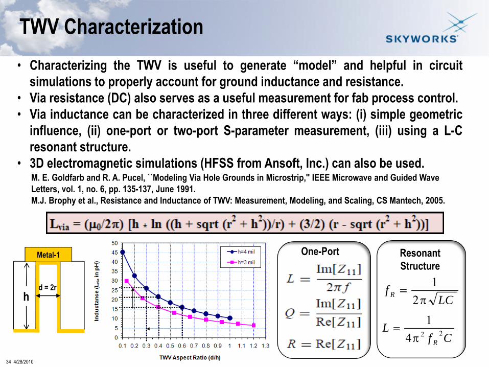
34 4/28/2010
TWV Characterization• Characterizing the TWV is useful to generate “model” and helpful in circuit
simulations to properly account for ground inductance and resistance.• Via resistance (DC) also serves as a useful measurement for fab process control.• Via inductance can be characterized in three different ways: (i) simple geometric
influence, (ii) one-port or two-port S-parameter measurement, (iii) using a L-Cresonant structure.
• 3D electromagnetic simulations (HFSS from Ansoft, Inc.) can also be used.
One-Port
LCf R π2
1=
ResonantStructure
CfL
R24
12π
=
Metal-1
hd = 2r
M. E. Goldfarb and R. A. Pucel, ``Modeling Via Hole Grounds in Microstrip,'' IEEE Microwave and Guided Wave Letters, vol. 1, no. 6, pp. 135-137, June 1991.M.J. Brophy et al., Resistance and Inductance of TWV: Measurement, Modeling, and Scaling, CS Mantech, 2005.

35 4/28/2010
Why Modeling and Simulation
• Consider “device application” when modeling! Most accurate model is not always the most useful model
• Must represent ALL devices used in design• Provide flexibility to design teams (device selections)• Educate designers on correct use of models.• Document the model vs. hardware fits
• Understand the behavior of the circuit as a function of changes to the circuit elements.
• “Simulate” before you “fabricate”!• Validate the “simulations” with the
circuit level measurements –emphasize the correct prediction of the behavior than the accuracy.
• Perform “corner” simulations.
• Feedback observed “anomalys” to processing• Physics is usually right• Translate circuit level needs to processing
groups• Modelers should understand what changes the
device
• Pay attention to modeling the variations, for e.g., variation of gm& Ic with Vbe, τf and Ccbwith Ic & Vce, in HBTs, sub-threshold characteristics of the FETs, etc.
• Include thermal effects and recommendation of “safe-operating area”.
Zampardi, Industrial Practices of Characterization and Modeling of III-V Technology , Oct.. 3, 2007, Boston, Mass.
(Zampardi, CMRF, 2007)
• Apply computational and device physics methods, combined with the measurements to generate “models”.

36 4/28/2010
Interactive Models – Designer Experience!
Simulation Setup
Variable Effects and Pareto ChartsDC and RF Characteristics, Ranges and Correlations
Circuit Schematics
All in ADSwork
interactivelythrough
built-in andcustomizedfunctions
(Yang 2008 PA Workshop)

37 4/28/2010
Physics Based Geometric Models
Features• Parameters calculated or directly
measured – forced to be physically okay.
• Single characterization database and test structure set.
• Scalable device models.• Re-use parameters for various
device blocks.• PCM-driven statistics and DOE
simulation.• Modularized-model code.
Benefits• No “golden” wafer required; model re-centering to electrical specs.• Allows sans GaAs explorations of circuit performance.• Less mask space, quicker model turn-around, behavioral consistency
across device suite (geometries and type).• Identify potential process issues or opportunities, multiple
geometries supported.• Allows mix-and-match models. Optimize materials for class of circuit
performance leveraging GaAs process.• Design FMEA, debug, and process sensitivity analysis. Constant
stream of PCM data “for-free” from in-line electrical test. Continuous feedback loop.
• Minimize number of files to maintain – less chance of error. Also provides flexibility to add new devices.
Physics Based Models REALLY Allow Us to Work Smarter, Not Harder
(Zampardi CMRF 2007)
38 4/28/2010
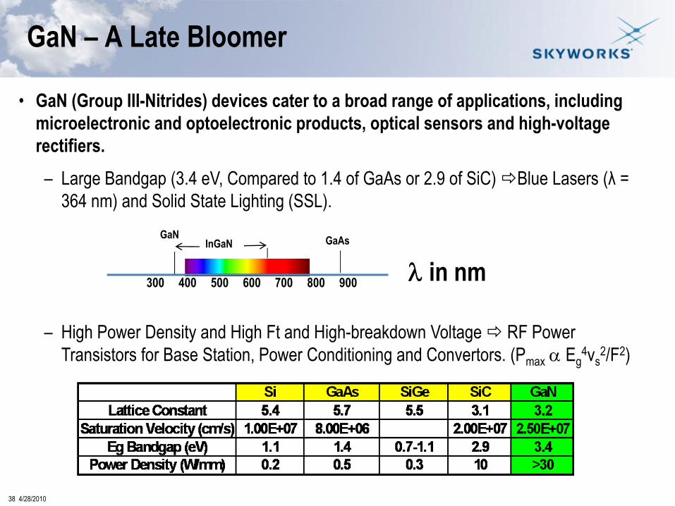
• GaN (Group III-Nitrides) devices cater to a broad range of applications, including microelectronic and optoelectronic products, optical sensors and high-voltage rectifiers.– Large Bandgap (3.4 eV, Compared to 1.4 of GaAs or 2.9 of SiC) Blue Lasers (λ =
364 nm) and Solid State Lighting (SSL).
– High Power Density and High Ft and High-breakdown Voltage RF Power Transistors for Base Station, Power Conditioning and Convertors. (Pmax α Eg
4vs2/F2)
GaN – A Late Bloomer
λ in nm400 500 600 700300 800 900
GaNInGaN GaAs
39 4/28/2010
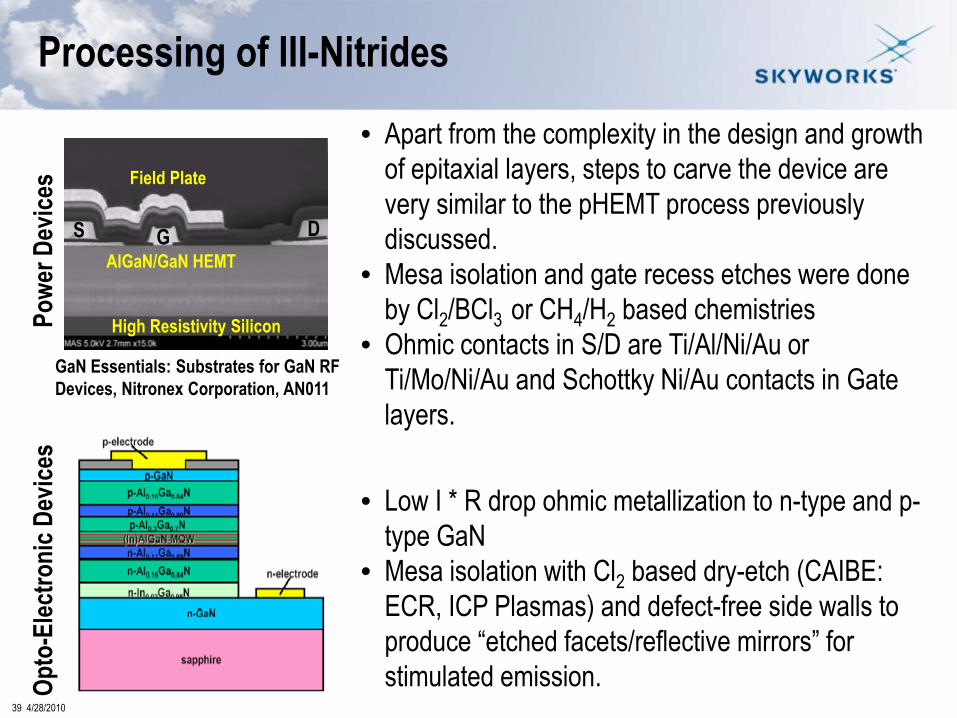
Processing of III-NitridesPo
wer D
evice
sOp
to-E
lectro
nic D
evice
s
• Apart from the complexity in the design and growth of epitaxial layers, steps to carve the device are very similar to the pHEMT process previously discussed.
• Mesa isolation and gate recess etches were done by Cl2/BCl3 or CH4/H2 based chemistries
• Ohmic contacts in S/D are Ti/Al/Ni/Au or Ti/Mo/Ni/Au and Schottky Ni/Au contacts in Gate layers.
GaN Essentials: Substrates for GaN RFDevices, Nitronex Corporation, AN011
GS D
Field Plate
High Resistivity Silicon
AlGaN/GaN HEMT
• Low I * R drop ohmic metallization to n-type and p-type GaN
• Mesa isolation with Cl2 based dry-etch (CAIBE: ECR, ICP Plasmas) and defect-free side walls to produce “etched facets/reflective mirrors” for stimulated emission.
40 4/28/2010
Processing Challenges of III-Nitrides
• The reproducibility in the growth of epitaxial layers due to theextremely high growth temperatures
• Gate recess etches – control of bias is crucial to achieve damage freesurface and sidewalls.
• Difficult to achieve good ohmic contacts due to the high bandgapcontact layer
• Appropriate wet clean or surface passivation is essential to get oxide-free surface prior to gate metallization.
• RTP at elevated temperatures (>750C) is needed to stabilize theohmic contacts as well as remove the dry-etch induced damage in thegate region.
• Progress in Etched Facet Technology for GaN and Blue Lasers, A.A. Behfar et al., CSMAX 2005• A. Weimar, A. Lell, G. Bruederl, S. Bader and V. Haerle. “Investigations of Low-Resistance Metal Contacts on p-
Type GaN using the Linear and Circular Transmission Line Method”, phys. stat. sol. (a) vol. 183, no. 169, 2001• From High Electron Mobility GaN/AlGaN Heterostructures to Blue-Violet InGaN Laser Diodes. Perspectives of MBE
for Nitride Optoelectronics, C. Skierbiszewski, ACTA PHYSICA POLONICA A , No. 4, Vol 108, page 635 (2005)
41 4/28/2010
Summary
• While III-V compound semiconductor device designs depend on proper engineering ofthe materials with different bandgaps, processing of those heterojunction materialspredominantly depends on the control of surface states, passivation, ohmic andSchottky contacts.
• Backend of line processing lacks “planarity” when used SiNx and polyimide as inter-level dielectrics, while BCB gives excellent planarity.
• 2 to 3 levels of gold metallization are commonly used as interconnect layers, but thesteady increase in gold price and year-over-year erosion in “selling price” of productswill lead way to alternate interconnect materials that are used in the Si industry.
• Though through wafer via process is matured for low inductance ground, Cu flipchip ismaking an inroad into the power amplifiers and front-end modules. Cu flipchip shouldbe a desirable alternative in GaN based devices for efficient heat transfer due to lack ofcost-effective TWV etch process in SiC substrates.
• GaN and InP technologies are slowly entering into high power and/or high speedcommercial markets. However, the price vs. performance seems to impede their rapidprogress.
42 4/28/2010
Acknowledgement
Thanks to:My colleagues in Skyworks’ Technology Development, Design, Operations and Quality for their contributions and help to further my knowledge in compound-semiconductor technology and to my management for their continued support.

43 4/28/2010
Backup

44 4/28/2010
• GaAs: Gallium Arsenide (III-V Compound Semiconductor)• BJT: Bipolar Junction Transistor• HBT: Heterojunction Bipolar Transistor• FET: Field Effect Transistor• CMOS: Complementary Metal Oxide Semiconductor (MOS) FET• pHEMT: Pseudomorphic High Electron Mobility Transistor• E/D pHEMT: Enhancement/Depletion Mode pHEMT Devices• BiCMOS: Combination of Bipolar and CMOS in the Same Wafer Processing • BiFET: HBT and FET Integrated on the Same Wafer• BiHEMT: HBT and pHEMT Integrated on the Same Wafer • MCM: Multi Chip Module (Multiple ICs in a Single Plastic Encapsulated Package)• PA and FEM: Power Amplifier and Front-end Modules• BCB: BenzoCycloButene (a Low Dielectric Constant Polymer Resin)• PBO: Poly Benzoxazole (a Low Dielectric Constant Polymer Film
Acronyms

45 4/28/2010
Useful References• David Pehlke and Dimitris Pavlids, “Evaluation of the Factors Determining HBT High-Frequency Performance by Direct Analysis of
S-Parameter Data,” IEEE Trans. On Microwave Theory and Techniques, Vol.40, No.12, Dec. 1992.• Modulation doping was discovered by R. Dingle, “New high-speed III-V devices for integrated circuits,” IEEE Trans. on Electron
Devices , 31, pp. 1662-1667, 1984.• H. Kroemer, Theory of wide-gap emitter for transistor, Proc. IRE, 45, 1535 (1957).• A Review of Semiconductor Heterojunctions, D. T. Calow et al., JOURNAL OF MATERIALS SCIENCE 2 (1967) 88-96• Methods for Monitoring Passivation Ledges in a Manufacturing Environment, P. Zampardi, L. Rushing, P. Ma, M.F. Chang, GaAs
Mantech 2002 Digest, paper #11B, pp. 225-228.• I. S. Vasil’evskiĭ et al., Electrical and structural properties of PHEMT Heterostructures based on AlGaAs/InGaAs/AlGaAs and δ-
doped on two sides, Semiconductors, 42, Number 9, page 1084-1091, 2008.• A Novel Optical Effect in InGaP Compound Collector Hetero-junction Bipolar Transistors, P. Zampardi and R.L. Pierson, 2002
Bipolar Circuits and Technology Meeting, pp. 232-235.• Development of High Breakdown Voltage InGaP/GaAs DHBTs, Jiang Li, Cristian Cismaru, Pete Zampardi, Eugene Babcock, Mike
Sun, and Ravi Ramanathan, and Kevin Stevens, 2007 GaAs Mantech Conference, Session 9, Paper 4.• A DOE Approach to Product Qualification For Linear Handset Power Amplifiers, P.J. Zampardi, D. Nelson, P. Zhu, C. Luo, S.
Rohlfing, and A. Jayapalan, 2004 Compound Semiconductor Mantech Conference, Miami, FL, pp. 91-94.• InGaP-GaAs HBT Statistical Modeling for RF Power Amplifier Designs, J. Hu, P. J. Zampardi, H. Shao, K. H. Kwok, C. Cismaru,
Digest of the Compound Semiconductor Integrated Circuit Symposium 2006, San Antonio, 2006, pp. 219-222.• An Innovative and Integrated Approach to III-V Circuit Design, Y. Yang, P. Zampardi, M. Fredriksson, J. Zu, S. Chen, G. Zheng, J.
Sifri, Microwave Journal, September 2008, pp. 136-156.• Practical Statistical Simulation for Efficient Circuit Design, Pete Zampardi, Yingying Yang, Juntao Hu, Bin Li, Mats Fredricksson, Kai
Kwok, Hongxiao Shao, IMS Workshop WMB, IMS Boston, June 2009.• Analysis and modeling on linearity for multi-throw TX/RX switches, C.J. Wei et al, 3rd MAPE intern’l conference, Beijing, Oct 27-29,
2009.• Enhanced High-Current VBIC model, C.J. Wei, J. Gering and Y. A. Tkachenko, SBMICRO 2004, Sept.9 2004 in Brazil, also
published in Trans MTT-53, No.4,2005 pp. 1235-1243.• DC/RF and statistic model of four terminal InGaP/GaAs BIFET for wireless communications, C. J. Wei, A. Metzger, Y. Zhu, C.
Cismaru, P. Zampardi, R. Ramanathan, and Y. A. Tkachenko, 2005 European Microwave Conference, Manchester, Sept. 2006.


![APPLICATION NOTE SKY77344-21 Power Amplifier … Notes/Skyworks...APPLICATION NOTE SKY77344 POWER AMPLIFIER MODULE – EVALUATION INFORMATION Skyworks Solutions, Inc. • Phone [781]](https://static.fdocuments.us/doc/165x107/5aeb162d7f8b9a90318c8547/application-note-sky77344-21-power-amplifier-notesskyworksapplication-note.jpg)


