Component and Connector Map - Compex Systems...DC Jack USB 2.0 Port USB 3.0 Type-C Port Ethernet...
5
hardware guide - AP .CP01 1 Compex Systems Pte Ltd | www.compex.com.sg | (+65) 6288 8220 | [email protected] | Last Updated: 02/01/2020 SL, LL, GS Copyright © Compex Systems. All rights reserved. COMPEX and the COMPEX logo, are registered trademarks of Compex Systems Pte Ltd. While every effort is made to ensure the information is accurate, Compex does not accept liability for any errors or mistakes that may arise. All specifications are subject to change without notice. Component and Connector Map M.2 (NGFF) “E Key“ Socket with MiniPCIe 3.0 Reset Button JTAG 20 Pin Connector SD Card Socket DC Jack USB 2.0 Port USB 3.0 Type-C Port Ethernet Port (2.5Gbps) Ethernet Port (1Gbps) 4x Ethernet Ports (1Gbps) 2.4GHz 2x U.FL Connectors 5GHz 2x U.FL Connectors
Transcript of Component and Connector Map - Compex Systems...DC Jack USB 2.0 Port USB 3.0 Type-C Port Ethernet...
hardware guide - AP.CP01
1Compex Systems Pte Ltd | www.compex.com.sg | (+65) 6288 8220 | [email protected] | Last Updated: 02/01/2020 SL, LL, GS
Copyright © Compex Systems. All rights reserved. COMPEX and the COMPEX logo, are registered trademarks of Compex Systems Pte Ltd.While every eff ort is made to ensure the information is accurate, Compex does not accept liability for any errors or mistakes that may arise.
All specifi cations are subject to change without notice.
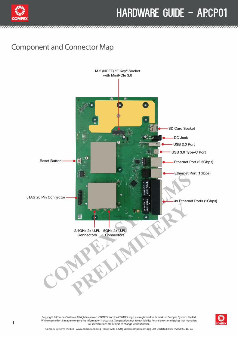
Component and Connector Map
M.2 (NGFF) “E Key“ Socket with MiniPCIe 3.0
Reset Button
JTAG 20 Pin Connector
SD Card Socket
DC Jack
USB 2.0 Port
USB 3.0 Type-C Port
Ethernet Port (2.5Gbps)
Ethernet Port (1Gbps)
4x Ethernet Ports (1Gbps)
2.4GHz 2x U.FL Connectors
5GHz 2x U.FL Connectors
hardware guide - AP.CP01
2Compex Systems Pte Ltd | www.compex.com.sg | (+65) 6288 8220 | [email protected] | Last Updated: 02/01/2020 SL, LL, GS
Copyright © Compex Systems. All rights reserved. COMPEX and the COMPEX logo, are registered trademarks of Compex Systems Pte Ltd.While every eff ort is made to ensure the information is accurate, Compex does not accept liability for any errors or mistakes that may arise.
All specifi cations are subject to change without notice.
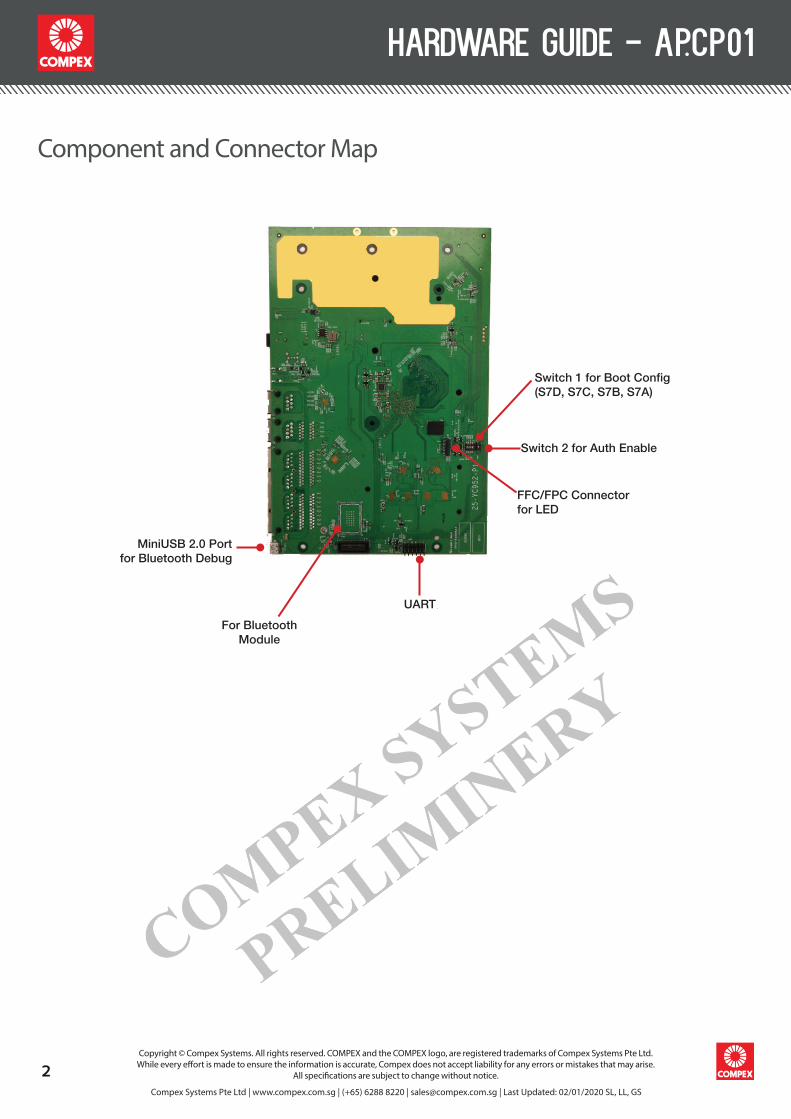
Component and Connector Map
Switch 1 for Boot Confi g(S7D, S7C, S7B, S7A)
Switch 2 for Auth Enable
FFC/FPC Connector for LED
UART
MiniUSB 2.0 Port for Bluetooth Debug
For Bluetooth Module
hardware guide - AP.CP01
3Compex Systems Pte Ltd | www.compex.com.sg | (+65) 6288 8220 | [email protected] | Last Updated: 02/01/2020 SL, LL, GS
Copyright © Compex Systems. All rights reserved. COMPEX and the COMPEX logo, are registered trademarks of Compex Systems Pte Ltd.While every effort is made to ensure the information is accurate, Compex does not accept liability for any errors or mistakes that may arise.
All specifications are subject to change without notice.
Power Requirements
DC Power 1x DC 12V for Main Board
Power Consumption TBD
UART Pin Assignment UART Interface
Pin Signal Pin Signal
1 DVDD_3V3 2 NC
3 UART_RXD_CONN 4 NC
5 NC 6 NC
7 NC 8 NC
9 UART_TXD_CONN 10 NC
11 GND 12 NC
JTAG Interface Pin AssignmentJTAG Interface
Pin Signal Pin Signal
1 VDD_1V8 2 VDD_1V8
3 JTAG_TRSTN 4 NC
5 JTAG_TDI 6 GND
7 JTAG_TMS 8 GND
9 JTAG_TCK 10 GND
11 PULL UP_1V8 12 GND
13 JTAG_TDO 14 GND
15 JTAG_SRSTN 16 GND
17 GND 18 GND
19 GND 20 GND
USB 2.0 Port Pin AssignmentUSB 2.0 Port
Pin Signal Pin Signal
1 VDD_5V_USB 2 CONN_USB1_DM
3 CONN_USB1_DP 4 GND
USB 3.0 Type-C Port Pin Assignment
USB 3.0 Type-C Port
Pin Signal Pin Signal
1 GND 2 GND
3 USBC_CONN_SSTX1_P 4 USBC_CONN_SSRX1_P
5 USBC_CONN_SSTX1_N 6 USBC_CONN_SSRX1_N
7 VBus_C_5V 8 VBus_C_5V
9 USBC_CONN_CC1 10 NC
11 USB0_DP 12 USB0_DM
13 USB0_DM 14 USB0_DP
15 NC 16 USBC_CONN_CC2
17 VBus_C_5V 18 VBus_C_5V
19 USBC_CONN_SSRX2_N 20 USBC_CONN_SSTX2_N
21 USBC_CONN_SSRX2_P 22 USBC_CONN_SSTX2_P
23 GND 24 GND
MiniUSB 2.0 Port Pin Assignment
FFC/FPC Connector for LED Pin Assignment
FFC/FPC Connector for LED
Pin Signal Pin Signal
1 VDD_1V8 2 VDD_3V3
3 P0_1000_LED 4 VDD_3V3
5 P1_1000_CONN 6 NAPA_LED
7 P2_1000_LED 8 NC
9 P3_1000_LED 10 USB0_LED
11 P4_1000_LED 12 WPS
13 PCIE_LED1 14 RESET_IN
15 5GM_LED 16 POWER_LED
17 2G_LED 18 NC
19 GND 20 GND
MiniUSB 2.0 Port
Pin Signal
1 NC
2 Q_USB_DM
3 Q_USB_DP
4 NC
5 GND

hardware guide - AP.CP01
4Compex Systems Pte Ltd | www.compex.com.sg | (+65) 6288 8220 | [email protected] | Last Updated: 02/01/2020 SL, LL, GS
Copyright © Compex Systems. All rights reserved. COMPEX and the COMPEX logo, are registered trademarks of Compex Systems Pte Ltd.While every effort is made to ensure the information is accurate, Compex does not accept liability for any errors or mistakes that may arise.
All specifications are subject to change without notice.
NGFF Slot Pin Assignment
SD Card Socket Pin Assignment
NGFF Slot
Pin Top Side Pin Bottom Side
1 GND 2 VDD_3V3
3 NC 4 VDD_3V3
5 NC 6 PCIE_LED1
7 GND 8 NC
9 NC 10 NC
11 NC 12 NC
13 NC 14 NC
15 VDD_5V 16 NC
17 VDD_5V 18 GND
19 VDD_5V 20 NC
21 VDD_5V 22 NC
23 VDD_5V
Mechanical Key E
33 GND 32 NC
35 PCIE_TX_P 34 NC
37 PCIE_TX_N 36 NC
39 GND 38 NC
41 PCIE_RX_P 40 NC
43 PCIE_RX_N 42 NC
45 GND 44 NC
47 PCIE_REFCLKP 46 NC
49 PCIE_REFCLKN 48 NC
51 GND 50 NC
53 PCIE_CLK_REQ 52 PCIE_PERST_N_3V3
55 PCIE_WAKE_3V3 54 NC
57 GND 56 NC
59 NC 58 NC
61 NC 60 NC
63 GND 62 NC
65 NC 64 NC
67 NC 66 NC
69 GND 68 NC
71 NC 70 NC
73 NC 72 VDD_3V3
75 GND 74 VDD_3V3
SD Card Socket
Pin Signal
1 SDC1_DATA_2
2 SDC1_DATA_3
3 SDC1_CMD
4 VDD_3V3
5 SDC1_CLK
6 GND
7 SDC1_DATA_0
8 SDC1_DATA_1
9 SDC1_DETECT
10 GND
GPIO Pin MappingGPIO Pin Mapping
Pin Signal Pin Signal
GPIO_0 AUDIO_MUTE_BUT GPIO_1 QPIC_BUSY_N
GPIO_2 MIC_VOL_M GPIO_3 QPIC_WE_N
GPIO_4 QPIC_RE_N GPIO_5 QPIC_DAT4
GPIO_6 QPIC_DAT5 GPIO_7 QPIC_DAT6
GPIO_8 QPIC_DAT7 GPIO_9 WPS
GPIO_10 QPIC_CLE_N GPIO_11 QPIC_NAND_CE_N
GPIO_12 QPIC_DAT1 GPIO_13 QPIC_DAT2
GPIO_14 QPIC_DAT3 GPIO_15 QPIC_DAT0
GPIO_16 MIC_KPD_PWR_N GPIO_17 QPIC_ALE
GPIO_18 KYPD_HOME_N GPIO_19 GND
GPIO_20 Boot_Config(PULL_DOWN) GPIO_21 MUTE_ON
GPIO_22 ADC_RST GPIO_23 WSA_SWR_CLK
GPIO_24 WSA_SWR_DATA GPIO_25 PWM_LED_RST
GPIO_26 Boot_Config(PULL_DOWN) GPIO_27 WSA_EN_R
GPIO_28 WSA_EN_L GPIO_29 PDM_CLK0
GPIO_30 PDM_DATA0 GPIO_31 PDM_CLK1
GPIO_32 PDM_DATA1 GPIO_33 EXT_MCLK2_ADC
GPIO_34 MIC_VOL_P GPIO_35 LED_5G
GPIO_36 PCIE0_WAKE GPIO_37 LED_2GS
GPIO_38 SPI0_CLK GPIO_39 SPI0_CS_NI
GPIO_40 SPI0_MISO GPIO_41 SPI0_MOSI
GPIO_42 BLSP2_SCL GPIO_43 BLSP2_SDA
GPIO_44 BLSP2_UART_RX GPIO_45 BLSP2_UART_TX
GPIO_46 BLSP5_SCL GPIO_47 BLSP5_SDA
GPIO_48 NC GPIO_49 Boot_Config(PULL_DOWN)
GPIO_50 LED_USB0 GPIO_51 BT_PRIORITY_PTA11
GPIO_52 WLA_ACTI_PTA12 GPIO_53 BT_ACT_PTA10
GPIO_54 Boot_Config(PULL_DOWN) GPIO_55 NC
GPIO_56 NC GPIO_57 NC
GPIO_58 NC GPIO_59 PCIE0_CLK_REQ
GPIO_60 PCIE0_RSTn GPIO_61 NC
GPIO_62 SD_DET GPIO_63 SD_WP
GPIO_64 MDC GPIO_65 MDIO
GPIO_66 SD_LDO_EN GPIO_67 NC
GPIO_68 NC GPIO_69 SPI_CLK_UART_RTSn
GPIO_70 SPI_CS_UART_CTSn GPIO_71 SPI_MISO_UART_RX
GPIO_72 SPI_MOSI_UART_TX GPIO_73 USB_OTG
GPIO_74 NC GPIO_75 Malibu_RESET
GPIO_76 NAPA_INT0 GPIO_77 NAPA_RESET
GPIO_78 QTZ_INT GPIO_79 QTZ_RESET
hardware guide - AP.CP01
5Compex Systems Pte Ltd | www.compex.com.sg | (+65) 6288 8220 | [email protected] | Last Updated: 02/01/2020 SL, LL, GS
Copyright © Compex Systems. All rights reserved. COMPEX and the COMPEX logo, are registered trademarks of Compex Systems Pte Ltd.While every effort is made to ensure the information is accurate, Compex does not accept liability for any errors or mistakes that may arise.
All specifications are subject to change without notice.
Boot Config Switch
Ethernet LAN/WAN Port Pin Assignment
Boot_Config Switch1(S7)
Boot_Config Boot up Interface Select
S7A S7B S7C
0 0 0 SPI NOR. (Default)
0 0 1 eMMC
0 1 0 QPIC, Parallel NAND
0 1 1 USB2.0
1 0 0 SPI-NOR-GPT
S7D Boot up Interface Select
0 Boot from code ram.(Default)
1 Boot from ROM
Boot_Config Switch2(S9)
Boot_Config Boot up Interface Select
0 No auth.(Default)
1 Auth is required.
Ethernet WAN /LAN Port (RJ45 1Gbps)
Pin Signal Pin Signal
1 1G_CH0_P 2 1G_CH0_N
3 1G_CH1_P 4 1G_CH2_P
5 1G_CH2_N 6 1G_CH1_N
7 1G_CH3_P 8 1G_CH3_N
Ethernet LAN Port Pin AssignmentEthernet LAN Port (RJ45 2.5Gbps)
Pin Signal Pin Signal
1 2.5G_CH0_P 2 2.5G_CH0_N
3 2.5G_CH1_P 4 2.5G_CH2_P
5 2.5G_CH2_N 6 2.5G_CH1_N
7 2.5G_CH3_P 8 2.5G_CH3_N