
comp_freq_lag.pdf
21
1 Phase Lag Compensator Design Using Bode Plots Prof. Guy Beale Electrical and Computer Engineering Department George Mason University Fairfax, Virginia Correspondence concerning this paper should be sent to Prof. Guy Beale, MSN 1G5, Electrical and Computer Engineering Department, George Mason University, 4400 University Drive, Fairfax, VA 22030-4444, USA. Fax: 703-993-1601. Email: [email protected]
Transcript of comp_freq_lag.pdf

1
Phase Lag Compensator Design
Using Bode Plots
Prof. Guy Beale
Electrical and Computer Engineering Department
George Mason University
Fairfax, Virginia
Correspondence concerning this paper should be sent to Prof. Guy Beale, MSN 1G5, Electrical and Computer Engineering
Department, George Mason University, 4400 University Drive, Fairfax, VA 22030-4444, USA. Fax: 703-993-1601. Email:
2
Contents
I INTRODUCTION 3
II DESIGN PROCEDURE 4
A. Compensator Structure . . . . . . . . . . . . . . . . . . . . . . . . . . . . . . . . . . . . 4
B. Outline of the Procedure . . . . . . . . . . . . . . . . . . . . . . . . . . . . . . . . . . . 4
C. Compensator Gain . . . . . . . . . . . . . . . . . . . . . . . . . . . . . . . . . . . . . . . 6
D. Making the Bode Plots . . . . . . . . . . . . . . . . . . . . . . . . . . . . . . . . . . . . 7
E. Gain Crossover Frequency . . . . . . . . . . . . . . . . . . . . . . . . . . . . . . . . . . . 7
F. Determination of α . . . . . . . . . . . . . . . . . . . . . . . . . . . . . . . . . . . . . . 8
G. Determination of zc and pc . . . . . . . . . . . . . . . . . . . . . . . . . . . . . . . . . . 10
III DESIGN EXAMPLE 12
A. Plant and Specifications . . . . . . . . . . . . . . . . . . . . . . . . . . . . . . . . . . . . 12
B. Compensator Gain . . . . . . . . . . . . . . . . . . . . . . . . . . . . . . . . . . . . . . . 12
C. The Bode Plots . . . . . . . . . . . . . . . . . . . . . . . . . . . . . . . . . . . . . . . . 13
D. Gain Crossover Frequency . . . . . . . . . . . . . . . . . . . . . . . . . . . . . . . . . . . 14
E. Calculating α . . . . . . . . . . . . . . . . . . . . . . . . . . . . . . . . . . . . . . . . . . 15
F. Compensator Zero and Pole . . . . . . . . . . . . . . . . . . . . . . . . . . . . . . . . . . 15
G. Evaluation of the Design . . . . . . . . . . . . . . . . . . . . . . . . . . . . . . . . . . . 15
H. Implementation of the Compensator . . . . . . . . . . . . . . . . . . . . . . . . . . . . . 17
I. Summary . . . . . . . . . . . . . . . . . . . . . . . . . . . . . . . . . . . . . . . . . . . . 19
References 21
List of Figures
1 Magnitude and phase plots for a typical lag compensator. . . . . . . . . . . . . . . . . . . 5
2 Bode plots for G(s) in Example 3. . . . . . . . . . . . . . . . . . . . . . . . . . . . . . . . 10
3 Bode plots for the plant after the steady-state error specification has been satisfied. . . . . 13
4 Bode plots for the compensated system. . . . . . . . . . . . . . . . . . . . . . . . . . . . . 16
5 Closed-loop frequency response magnitudes for the example. . . . . . . . . . . . . . . . . . 17
6 Step and ramp responses for the closed-loop systems. . . . . . . . . . . . . . . . . . . . . . 18

3
I. INTRODUCTION
The purpose of phase lag compensator design in the frequency domain generally is to satisfy specifi-
cations on steady-state accuracy and phase margin. There may also be a specification on gain crossover
frequency or closed-loop bandwidth. A phase margin specification can represent a requirement on relative
stability due to pure time delay in the system, or it can represent desired transient response characteristics
that have been translated from the time domain into the frequency domain.
The overall philosophy in the design procedure presented here is for the compensator to adjust the
system’s Bode magnitude curve to establish a gain-crossover frequency, without disturbing the system’s
phase curve at that frequency and without reducing the zero-frequency magnitude value. In order for
phase lag compensation to work in this context, the following two characteristics are needed:
• the uncompensated Bode phase curve must pass through the correct value to satisfy the phase
margin specification at some acceptable frequency;
• the Bode magnitude curve (after the steady-state accuracy specification has been satisfied) must
be above 0 db at the frequency where the uncompensated phase shift has the correct value to
satisfy the phase margin specification (otherwise no compensation other than additional gain is
needed).
If the compensation is to be performed by a single-stage compensator, then it must also be possible to drop
the magnitude curve down to 0 db at that frequency without using excessively large component values.
Multiple stages of compensation can be used, following the same procedure as shown below. Multiple
stages are needed when the amount that the Bode magnitude curve must be moved down is too large for
a single stage of compensation. More is said about this later.
The gain crossover frequency and closed-loop bandwidth for the lag-compensated system will be lower
than for the uncompensated plant (after the steady-state error specification has been satisfied), so the
compensated system will respond more slowly in the time domain. The slower response may be regarded
as a disadvantage, but one benefit of a smaller bandwidth is that less noise and other high frequency
signals (often unwanted) will be passed by the system. The smaller bandwidth will also provide more
stability robustness when the system has unmodeled high frequency dynamics, such as the bending modes
in aircraft and spacecraft. Thus, there is a trade-off between having the ability to track rapidly varying
reference signals and being able to reject high-frequency disturbances.
The design procedure presented here is basically graphical in nature. All of the measurements needed
can be obtained from accurate Bode plots of the uncompensated system. If data arrays representing
the magnitudes and phases of the system at various frequencies are available, then the procedure can be
done numerically, and in many cases automated. The examples and plots presented here are all done
in MATLAB, and the various measurements that are presented in the examples are obtained from the
various data arrays.

4
The primary references for the procedures described in this paper are [1] – [3]. Other references that
contain similar material are [4] – [11].
II. DESIGN PROCEDURE
A. Compensator Structure
The basic phase lag compensator consists of a gain, one pole, and one zero. Based on the usual electronic
implementation of the compensator [3], the specific structure of the compensator is:
Gc lag(s) = Kc
[1α· (s + zc)(s + pc)
](1)
= Kc(s/zc + 1)(s/pc + 1)
= Kc(τs + 1)(ατs + 1)
with
zc > 0, pc > 0, α , zc
pc> 1, τ =
1zc
=1
αpc(2)
Figure 1 shows the Bode plots of magnitude and phase for a typical lag compensator. The values in
this example are Kc = 1, pc = 0.4, and zc = 2.5, so α = 2.5/0.4 = 6.25. Changing the gain merely moves
the magnitude curve by 20∗ log10 |Kc|. The major characteristics of the lag compensator are the constant
attenuation in magnitude at high frequencies and the zero phase shift at high frequencies. The large
negative phase shift that is seen at intermediate frequencies is undesired but unavoidable. Proper design
of the compensator requires placing the compensator pole and zero appropriately so that the benefits of
the magnitude attenuation are obtained without the negative phase shift causing problems. The following
paragraphs show how this can be accomplished.
B. Outline of the Procedure
The following steps outline the procedure that will be used to design the phase lag compensator to
satisfy steady-state error and phase margin specifications. Each step will be described in detail in the
subsequent sections.
1. Determine if the System Type N needs to be increased in order to satisfy the steady-state error
specification, and if necessary, augment the plant with the required number of poles at s = 0.
Calculate Kc to satisfy the steady-state error.
2. Make the Bode plots of G(s) = KcGp(s)/s(Nreq−Nsys).
3. Design the lag portion of the compensator:
(a) determine the frequency where G(jω) would satisfy the phase margin specification if that
frequency were the gain crossover frequency;
(b) determine the amount of attenuation that is required to drop the magnitude of G(jω) down
to 0 db at that same frequency, and compute the corresponding α;

5
10−3
10−2
10−1
100
101
102
103
−20
−18
−16
−14
−12
−10
−8
−6
−4
−2
0
Frequency (r/s)
Mag
nitu
de (
db)
Lag Compensator Magnitude, pc = 0.4, z
c = 2.5, K
c = 1
10−3
10−2
10−1
100
101
102
103
−50
−45
−40
−35
−30
−25
−20
−15
−10
−5
0
Frequency (r/s)
Pha
se (
deg)
Lag Compensator Phase, pc = 0.4, z
c = 2.5, K
c = 1
Fig. 1. Magnitude and phase plots for a typical lag compensator.

6
(c) using the value of α and the chosen gain crossover frequency, compute the lag compensator’s
zero zc and pole pc.
4. If necessary, choose appropriate resistor and capacitor values to implement the compensator
design.
C. Compensator Gain
The first step in the design procedure is to determine the value of the gain Kc. In the procedure that
I will present, the gain is used to satisfy the steady-state error specification. Therefore, the gain can be
computed from
Kc =ess plant
ess specified=
Kx required
Kx plant(3)
where ess is the steady-state error for a particular type of input, such as step or ramp, and Kx is the
corresponding error constant of the system. Defining the number of open-loop poles of the system G(s)
that are located at s = 0 to be the System Type N , and restricting the reference input signal to having
Laplace transforms of the form R(s) = A/sq, the steady-state error and error constant are (assuming that
the closed-loop system is bounded-input, bounded-output stable)
ess = lims→0
[AsN+1−q
sN + Kx
](4)
where
Kx = lims→0
[sNG(s)
](5)
For N = 0, the steady-state error for a step input (q = 1) is ess = A/ (1 + Kx). For N = 0 and q > 1,
the steady-state error is infinitely large. For N > 0, the steady-state error is ess = A/Kx for the input
type that has q = N +1. If q < N +1, the steady-state error is 0, and if q > N +1, the steady-state error
is infinite.
The calculation of the gain in (3) assumes that the given system Gp(s) is of the correct Type N to
satisfy the steady-state error specification. If it is not, then the compensator must have one or more poles
at s = 0 in order to increase the overall System Type to the correct value. Once this is recognized, the
compensator poles at s = 0 can be included with the plant Gp(s) during the rest of the design of the lag
compensator. The values of Kx in (5) and of Kc in (3) would then be computed based on Gp(s) being
augmented with these additional poles at the origin.
Example 1: As an example, consider the situation where a steady-state error of ess specified = 0.05
is specified when the reference input is a unit ramp function (q = 2). This requires an error constant
Kx required = 1/0.05 = 20. Assume that the plant is Gp(s) = 200/ [(s + 4) (s + 5)], which is Type 0.
Then the compensator must have one pole at s = 0 in order to satisfy this specification. When Gp(s) is
augmented with this compensator pole at the origin, the error constant of Gp(s)/s is Kx = 200/ (4 · 5) =

7
10, so the steady-state error for a ramp input is ess plant = 1/10 = 0.1. Therefore, the compensator
requires a gain having a value of Kc = 0.1/0.05 = 20/10 = 2. ¨
Once the compensator design is completed, the total compensator will have the transfer function
Gc lag(s) =Kc
s(Nreq−Nsys)· (s/zc + 1)(s/pc + 1)
(6)
where Nreq is the total required number of poles at s = 0 to satisfy the steady-state error specification,
and Nsys is the number of poles at s = 0 in Gp(s). In the above example, Nreq = 2 and Nsys = 1.
D. Making the Bode Plots
The next step is to plot the magnitude and phase as a function of frequency ω for the series combination
of the compensator gain (and any compensator poles at s = 0) and the given system Gp(s). This transfer
function will be the one used to determine the values of the compensator’s pole and zero and to determine
if more than one stage of compensation is needed. The magnitude |G (jω)| is generally plotted in decibels
(db) vs. frequency on a log scale, and the phase ∠G (jω) is plotted in degrees vs. frequency on a log scale.
At this stage of the design, the system whose frequency response is being plotted is
G(s) =Kc
s(Nreq−Nsys)·Gp(s) (7)
If the compensator does not have any poles at the origin, the gain Kc just shifts the plant’s magnitude
curve by 20 ∗ log10 |Kc| db at all frequencies. If the compensator does have one or more poles at the
origin, the slope of the plant’s magnitude curve also is changed by −20 db/decade at all frequencies for
each compensator pole at s = 0. In either case, satisfying the steady-state error sets requirements on the
zero-frequency portion of the magnitude curve, so the rest of the design procedure will manipulate the
magnitude and phase curves without changing the magnitude curve at zero frequency. The plant’s phase
curve is shifted by −90 (Nreq −Nsys) at all frequencies, so if the plant Gp(s) has the correct System
Type, then the compensator does not change the phase curve at this point in the design.
The remainder of the design is to determine (s/zc + 1) / (s/pc + 1). The values of zc and pc will be
chosen to satisfy the phase margin and crossover frequency specifications. Note that at ω = 0, the
magnitude |(jω/zc + 1) / (jω/pc + 1)| = 1 ⇒ 0 db and the phase ∠ (jω/zc + 1) / (jω/pc + 1) = 0 degrees.
Therefore, the low-frequency parts of the curves just plotted will be unchanged, and the steady-state error
specification will remain satisfied. The Bode plots of the complete compensated system Gc lag(jω)Gp(jω)
will be the sum, at each frequency, of the plots made in this step of the procedure and the plots of
(jω/zc + 1) / (jω/pc + 1).
E. Gain Crossover Frequency
Now we will find the frequency that will become the gain crossover frequency for the compensated
system. The gain crossover frequency is defined to be that frequency ωx where |G (jωx)| = 1 in absolute
8
value or |G (jωx)| = 0 in db. The purpose of the lag compensator’s pole–zero combination is to drop the
magnitude of the transfer function G (jω), defined in (7), down to 0 db at the appropriate frequency to
satisfy the phase margin specification.
Since the goal of the lag compensator is to adjust the magnitude curve as needed without shifting the
phase curve, the frequency that is chosen for the compensated gain crossover frequency is that frequency
where the phase shift of the system given in (7) has the correct value to satisfy the phase margin spec-
ification. Generally, the specified phase margin is increased 5–10 to account for the fact that the lag
compensator is not ideal, and the phase curve of the system in (7) is actually shifted by a small amount
at the chosen frequency.
Therefore, the compensated gain crossover frequency ωx compensated is that frequency where
∠[
Kc
s(Nreq−Nsys)·Gp(s)
]= −180 + PMspecified + 10 (8)
where PMspecified is the specification on phase margin (in degrees), and a safety factor of 10 is being
used.
Example 2: For example, if the specified phase margin is 40, then ωx compensated is chosen to be that
frequency where the phase shift in (8) evaluates to −180 + 40 + 10 = −130. This ωx compensated is
the frequency where the magnitude of the compensated system |Gc lag (jω) Gp (jω)| = 1 ⇒ 0 db, with
Gc lag(s) given by (6). ¨
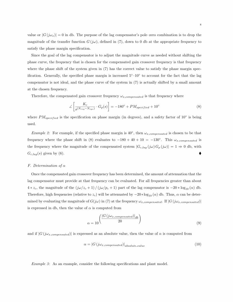
F. Determination of α
Once the compensated gain crossover frequency has been determined, the amount of attenuation that the
lag compensator must provide at that frequency can be evaluated. For all frequencies greater than about
4 ∗ zc, the magnitude of the (jω/zc + 1) / (jω/pc + 1) part of the lag compensator is −20 ∗ log10 (α) db.
Therefore, high frequencies (relative to zc) will be attenuated by −20∗ log10 (α) db. Thus, α can be deter-
mined by evaluating the magnitude of G(jω) in (7) at the frequency ωx compensated. If |G (jωx compensated)|is expressed in db, then the value of α is computed from
α = 10
0@ |G (jωx compensated)|db
20
1A
(9)
and if |G (jωx compensated)| is expressed as an absolute value, then the value of α is computed from
α = |G (jωx compensated)|absolute value (10)
Example 3: As an example, consider the following specifications and plant model.

9
• PMspecified ≥ 40;
• ess specified = 0.05 for a ramp input.
Gp(s) =60
(s + 1) (s + 2) (s + 3)(11)
Since the plant is Type 0 and the steady-state error specification is for a ramp input, the compensator
must have one pole at s = 0. The compensator must also have a gain Kc = 2 in order to satisfy the
steady-state error specification, since Kx plant = 10, and Kx required = 20. Thus, the system G(s) for this
example is
G(s) =120
s (s + 1) (s + 2) (s + 3)(12)
Once the Bode plots of G(s) are made, shown in Fig. 2, expression (8) tells us that we should search
for the frequency where the phase shift is −130. This occurs at approximately 0.39 r/s; this frequency
is ωx compensated. At this frequency, the magnitude of G(s) can be read directly from the graph, and
its value is |G (jωx compensated)| = 33.4 db. Converting this to an absolute value using (9) gives us
the value α = 46.6. Therefore, the compensator’s pole–zero combination will be related by the ratio
zc/pc = α = 46.6. ¨
The value of α = 46.6 in this example is generally considered to be too large for a single stage of lag
compensation. The values of the resistors and capacitors needed to implement the compensator increase
with the value of α, as does the maximum amount of negative phase shift that the compensator produces.
Many references state that α ≤ 10 should be used for the lag compensator to prevent excessively large
component values and to limit the amount of undesired phase shift.
If this limit is used, and α > 10, then multiple stages of compensation are required. An easy way to
accomplish this is to design identical compensators (that will be implemented in series), so that each stage
of the compensator attenuates the magnitude of G (jω) by the same amount. Since the magnitude of a
product of transfer functions is the product of the individual magnitudes, the value of α for each of the
stages is
αstage = nstage√
αtotal (13)
where nstage is the number of stages to be used in the compensator, given by
nstage =
2, 10 < αtotal ≤ 100
3, 100 < αtotal ≤ 1000...
...
n, 10n−1 < αtotal ≤ 10n
(14)
Example 4: If the value α = 46.6 in Example 3 is assumed to be too large, two stages of compensation
can be used. Each stage would be given an attenuation of αstage=√
46.6 = 6.83. When the compensator

10
10−2
10−1
100
101
102
103
−400
−350
−300
−250
−200
−150
−100
−50
0
50
100
Frequency (r/s)
Mag
nitu
de (
db)
& P
hase
(de
g)
−130 deg
33.4 db
G(s) = 120/[s(s+1)(s+2)(s+3)]
w = 0.39 r/s
Fig. 2. Bode plots for G(s) in Example 3.
is implemented, the gain Kc = 2 could also be divided evenly between the two stages in the same fashion,
with Kc stage =√
2 = 1.414. ¨
G. Determination of zc and pc
The last step in the design of the transfer function for the lag compensator is to determine the values of
the pole and zero. We have already determined their ratio α, so only one of those terms is a free variable.
We will choose to place the compensator zero and then compute the pole location from pc = zc/α. Figure
1 is the key to deciding how to place zc. In that example, zc = 2.5, and at the frequency ω = 25 r/s (one
decade above the frequency corresponding to the value of zc), the magnitude is constant at −15.9 db, and
the phase shift of the compensator is −4.7. Because of the nature of the tangent of an angle, the phase
shift for a single-stage lag compensator will never be more negative than −5.7 at a frequency one decade
above the location of the compensator zero. In determining the compensated gain crossover frequency
11
in (8), we added 10 to the specified phase margin to account for phase shift from the compensator at
ωx compensated. Therefore, if the value of the compensator zero is chosen to correspond to the frequency one
decade below ωx compensated, then the phase margin will always be satisfied. Smaller values of zc can also
be used. Lower limits on the values of zc and pc are governed by the values of the corresponding electronic
components used to implement the compensator.1 The compensator’s zero and pole are computed from
zc ≤ ωx compensated
10, pc =
zc
α(15)
Example 5: Continuing from Example 3, with ωx compensated = 0.39 r/s and α = 46.6, acceptable values
for the compensator’s zero and pole are zc = 0.39/10 = 0.039 and pc = 0.039/46.6 = 8.37 · 10−4. The
complete compensator for these examples is
Gc lag(s) =2 (s/0.039 + 1)
s (s/8.37 · 10−4 + 1)=
0.0429 (s + 0.039)s (s + 8.37 · 10−4)
(16)
If the compensator is split into two stages, as in Example 4, then zc = 0.39/10 = 0.039 and pc =
0.039/6.83 = 5.71 · 10−3 can be used for the zero and pole for each stage of the compensator.
Placing the zero at zc = 0.039 and using two stages of compensator uses up all of the 10 safety factor
included in expression (8). To assure that the phase margin specification will be satisfied when using
multiple stages of lag compensation, I use the following technique for determining the compensator’s zero
and pole:
zc =ωx compensated
10nstage, pc =
zc
αstage(17)
which for this example gives zc = 1.95 · 10−2 and pc = 2.86 · 10−3, and the total compensator is
Gc lag(s) =2
(s/1.95 · 10−2 + 1
)2
s (s/2.86 · 10−3 + 1)2=
1s·[
1.414(s/1.95 · 10−2 + 1
)
(s/2.86 · 10−3 + 1)
]2
(18)
=1s·[
0.207(s + 1.95 · 10−2
)
(s + 2.86 · 10−3)
]2
with nstage = 2 and αstage = 6.83. ¨
The lag compensator is ideal in the sense that any amount of magnitude attenuation can be theoretically
provided by a single stage of compensation since α = |G (jωx−compensated)|abs val > 1. The effects of
negative phase shift from the compensator can be made negligible by making zc suitably small. The
need for multiple stages of compensation is dictated by implementation considerations in the choice of
electronic component values.
1The textbook by Ogata [3] has a table in Chapter 5 that shows op amp circuits for various types of compensators.

12
III. DESIGN EXAMPLE
A. Plant and Specifications
The plant to be controlled is described by the transfer function
Gp(s) =280 (s + 0.5)
s (s + 0.2) (s + 5) (s + 70)(19)
=2 (s/0.5 + 1)
s (s/0.2 + 1) (s/5 + 1) (s/70 + 1)
This is a Type 1 system, so the closed-loop system will have zero steady-state error for a step input, and
a non-zero, finite steady-state error for a ramp input (assuming that the closed-loop system is stable). As
shown in the next section, the error constant for a ramp input is Kx−plant = 2. At low frequencies, the
plant has a magnitude slope of −20 db/decade, and at high frequencies the slope is −60 db/decade. The
phase curve starts at −90 and ends at −270.
The specifications that must be satisfied are:
• steady-state error for a ramp input ess specified ≤ 0.02;
• phase margin PMspecified ≥ 45.
These specifications do not impose any explicit requirements on the gain crossover frequency or on the
type of compensator that should be used. It may be possible to use either lag or lead compensation for
this problem, or a combination of the two, but we will use the phase lag compensator design procedure
described above. The following paragraphs will illustrate how the procedure is applied to design the
compensator for this system that will allow the specifications to be satisfied.
B. Compensator Gain
The given plant is Type 1, and the steady-state error specification is for a ramp input, so the compen-
sator does not need to have any poles at s = 0. Only the gain Kc needs to be computed for steady-state
error. The steady-state error for a ramp input for the given plant is
Kx plant = lims→0
[s · 280 (s + 0.5)
s (s + 0.2) (s + 5) (s + 70)
](20)
= lims→0
[s · 2 (s/0.5 + 1)
s (s/0.2 + 1) (s/5 + 1) (s/70 + 1)
]
= 2
ess plant =1
Kx= 0.5 (21)
Since the specified value of the steady-state error is 0.02, the required error constant is Kx required = 50.
Therefore, the compensator gain is
Kc =ess plant
ess specified=
0.50.02
= 25 (22)
=Kx required
Kx plant=
502
= 25

13
10−3
10−2
10−1
100
101
102
103
104
−300
−250
−200
−150
−100
−50
0
50
100
Frequency (r/s)
Mag
nitu
de (
db)
& P
hase
(de
g)
Bode Plots for Gp(s) and K
cG
p(s), K
c = 25
−125 deg
17.4 db
2.45 r/s
Fig. 3. Bode plots for the plant after the steady-state error specification has been satisfied.
This value for Kc will satisfy the steady-state error specification, and the rest of the compensator design
will focus on the phase margin specification.
C. The Bode Plots
The magnitude and phase plots for KcGp(s) are shown in Fig. 3. The dashed magnitude curve is for
Gp(s) and illustrates the effect that Kc has on the magnitude. Specifically, |KcGp (jω)| is 20 log10 |25| ≈ 28
db above the curve for |Gp (jω)| at all frequencies. The phase curve is unchanged when the steady-state
error specification is satisfied since the compensator does not have any poles at the origin.
The horizontal dashed line at −125 is included in the figure to indicate the phase shift that will satisfy
the phase margin specification (+10) when the frequency at which this phase shift occurs is made the
gain crossover frequency. The vertical dashed line indicates that frequency.
Note that the gain crossover frequency of KcGp(s) is larger than that for Gp(s); the crossover frequency

14
has moved to the right in the graph. The closed-loop bandwidth will have increased in a similar manner.
The phase margin has decreased due to Kc, so satisfying the steady-state error has made the system less
stable; in fact, increasing Kc in order to decrease the steady-state error can even make the closed-loop
system unstable. Maintaining stability and achieving the desired phase margin is the task of the pole–zero
combination in the compensator.
Our ability to graphically determine values for ωx compensated and α obviously depends on the accuracy
and resolution of the Bode plots of |KcGp (jω)|. High resolution plots like those obtained from MATLAB
allow us to obtain reasonably accurate measurements. Rough, hand-drawn sketches would yield much
less accurate results and might be used only for first approximations to the design. Being able to access
the actual numerical data allows for even more accurate results than the MATLAB-generated plots. The
procedure that I use when working in MATLAB generates the data arrays for frequency, magnitude, and
phase from the following instructions:
w = logspace(N1,N2,1+100*(N2-N1));
[mag,ph] = bode(num,den,w);
semilogx(w,20*log10(mag),w,ph),grid
where N1= log10 (ωmin), N2 = log10 (ωmax), and num, den are the numerator and denominator polynomials,
respectively, of KcGp (s). For this example,
N1= −3;
N2= 4;
num= 25 ∗ 280 ∗[
1 0.5];
den=conv([
1 0.2 0], conv
([1 5
],
[1 70
]));
The data arrays mag, ph, and w can be searched to obtain the various values needed during the design
of the compensator.
D. Gain Crossover Frequency
As mentioned above, the compensated gain crossover frequency is selected to be the frequency at which
the phase shift ∠KcGp (jω) = −125. This value of phase shift was computed from (8), which allows
the phase margin specification to be satisfied, taking into account the non-ideal characteristics of the
compensator.
From the phase curve plotted in Fig. 3, this value of phase shift occurs approximately midway between 2
r/s and 3 r/s. Since the midpoint frequency on a log scale is the geometric mean of the two end frequencies,
an estimate of the desired frequency is ω =√
2 · 3 = 2.45 r/s. Searching the MATLAB data arrays storing
the frequency and phase information gives the value ω = 2.4531 r/s (using 100 equally-spaced values per
decade of frequency), so the estimate obtained from the graph is very accurate in this example.

15
E. Calculating α
The lag compensator must attenuate |KcGp (jω)| so that it has the value 0 db at frequency ω = 2.45
r/s. From the magnitude curve in Fig. 3, it is easy to see that |KcGp (j2.45)|db is between 15 db and
20 db. An accurate measurement of the graph would provide a value of 17.4 db for the magnitude. The
corresponding value of α is calculated by using (9), and the result is α = 7.435, which can be easily
implemented with a single stage of compensation. A search of the MATLAB data array storing the
magnitudes (as absolute values) yields 7.435 as the element corresponding to ω = 2.45 r/s, so equation
(10) is verified.
F. Compensator Zero and Pole
Now that we have values for ωx compensated and α, we can determine the values for the compensator’s
zero and pole from (15). The values that we obtain are zc = 0.245 and pc = 0.033. The final compensator
for this example is
Gc lag(s) =25 (s/0.245 + 1)(s/0.033 + 1)
=25 (4.08s + 1)(30.3s + 1)
(23)
=3.37 (s + 0.245)
(s + 0.033)
G. Evaluation of the Design
The frequency response magnitude and phase of the compensated system Gc lag(s)Gp(s) are shown in
Fig. 4. The magnitude is attenuated at high frequencies, passing through 0 db at approximately 2.45 r/s,
so the compensated gain crossover frequency has been established at the desired value. The compensated
phase curve is seen to be nearly back to the uncompensated curve at ωx compensated. The lag compensator
is contributing approximately −4.9 at that frequency, so the phase margin specification is satisfied.
To illustrate the effects of the compensator on closed-loop bandwidth, the magnitudes of the closed-
loop systems are plotted in Fig. 5. The smallest bandwidth occurs with the plant Gp(s). Including the
compensator gain Kc > 1 increases the bandwidth and the size of the resonant peak. Significant overshoot
in the time-domain step response should be expected from the closed-loop system with Kc = 25. Including
the entire lag compensator reduces the bandwidth and the resonant peak, relative to that with KcGp(s).
The step response overshoot in the lag-compensated system should be similar to the uncompensated
system, but the settling time will be less due to the larger bandwidth.
The major difference in the time-domain responses between the uncompensated system and the lag-
compensated system is in the ramp response. The steady-state error is reduced by a factor of 25 due
to Kc. The closed-loop step and ramp responses are shown in Fig. 6. A closed-loop steady-state error
ess = 0.02 is achieved both for KcGp(s) and Gc lag(s)Gp(s). The faster of those two responses is from
KcGp(s).

16
10−3
10−2
10−1
100
101
102
103
104
−300
−250
−200
−150
−100
−50
0
50
100
wx−compensated
Frequency (r/s)
Mag
nitu
de (
db)
& P
hase
(de
g)
Bode Plots for Lag−Compensated System
KcG
p(s)
KcG
p(s)
Fig. 4. Bode plots for the compensated system.
To see some of the effects of the value of the compensator’s zero, a second lag compensator was designed.
The same specifications were used; the only difference between the two designs is that the zero of the new
compensator was placed two decades in frequency below the compensated gain crossover frequency, rather
than one decade. The value of the compensator pole also changed as a result. The new compensator is
Gc lag 2(s) =25 (s/0.0245 + 1)(s/0.0033 + 1)
=25 (40.8s + 1)
(303s + 1)(24)
=3.37 (s + 0.0245)
(s + 0.0033)
This new compensator reduces the percent overshoot to a step input and provides additional phase margin.
The added phase margin is due to the fact that the compensator’s phase shift is virtually zero at a
frequency two decades above zc. Both of these characteristics are good. The drawbacks to using the
second compensator are the increased values of the electronic components (a problem particularly with
the capacitors) and the increase in the settling time of the ramp response. The time it takes the unit

17
10−3
10−2
10−1
100
101
102
103
104
−200
−150
−100
−50
0
50
Frequency (r/s)
Mag
nitu
de (
db)
Closed−Loop Magnitudes for Gp(s), K
cG
p(s), and G
c(s)G
p(s)
KcG
p(s)
Gp(s)
Fig. 5. Closed-loop frequency response magnitudes for the example.
ramp response to reach a value 0.02 less than the input (ess) increases from approximately 6.3 seconds
with Gc lag(s) to 316 seconds with Gc lag 2(s). Trade-offs such as this typically have to be made during
the design of any control system.
H. Implementation of the Compensator
Ogata [3] presents a table showing analog circuit implementations for various types of compensators.
The circuit for phase lag is the series combination of two inverting operational amplifiers. The first
amplifier has an input impedance that is the parallel combination of resistor R1 and capacitor C1 and a
feedback impedance that is the parallel combination of resistor R2 and capacitor C2. The second amplifier
has input and feedback resistors R3 and R4, respectively.

18
0 1 2 3 4 5 6 7 8 9 100
0.2
0.4
0.6
0.8
1
1.2
1.4
1.6
1.8
Gp(s)
KcG
p(s)
Gc(s)G
p(s)
Time (s)
Am
plitu
de
Closed−Loop Step Responses
0 1 2 3 4 5 6 7 8 9 100
1
2
3
4
5
6
7
8
9
10
Gp(s)
Time (s)
Am
plitu
de
Closed−Loop Ramp Responses
Fig. 6. Step and ramp responses for the closed-loop systems.

19
Assuming that the op amps are ideal, the transfer function for this circuit is
Vout(s)Vin(s)
=R2R4
R1R3· (sR1C1 + 1)(sR2C2 + 1)
(25)
=R2R4
R1R3· R1C1
R2C2· (s + 1/R1C1)(s + 1/R2C2)
Comparing (25) with Gc lag(s) in (1) shows that the following relationships hold:
Kc =R2R4
R1R3, τ = R1C1, ατ = R2C2 (26)
zc = 1/R1C1, pc = 1/R2C2, α =zc
pc=
R2C2
R1C1
Equation (26) shows that decreasing the value of zc and/or increasing the value of α leads to larger
component values. Since space on printed circuit boards is generally restricted, upper limits are imposed
on the values of the resistors and capacitors. Thus, decisions have to be made concerning the values of zc
and pc and the number of stages of compensation that are used.
Equations (25) and (26) are the same as for a lag compensator. The only difference is that α < 1 for a
lead compensator and α > 1 for a lag compensator, so the relative values of the components change.
To implement the compensator using the circuit in [3], note that there are 6 unknown circuit elements
(R1, C1, R2, C2, R3, R4) and 3 compensator parameters (Kc, zc, pc). Therefore, three of the circuit
elements can be chosen to have convenient values. To implement the original lag compensator Gc lag(s)
in this design example, we can use the following values
C1 = C2 = 0.47 µF = 4.7 · 10−7 F, R3 = 10 KΩ = 104 Ω (27)
R1 =1
zcC1= 8.67 MΩ = 8.67 · 106 Ω
R2 =1
pcC2= 64.4 MΩ = 6.44 · 107 Ω
R4 =R3Kc
α= 33.6 KΩ = 3.36 · 104 Ω
where the elements in the first row of (27) were specified and the remaining elements were computed from
(26).
I. Summary
In this example, the phase lag compensator in (23) is able to satisfy both of the specifications of the
system given in (19). In addition to satisfying the phase margin and steady-state error specifications, the
lag compensator also produced a step response with shorter settling time.
In summary, phase lag compensation can provide steady-state accuracy and necessary phase margin
when the Bode magnitude plot can be dropped down at the frequency chosen to be the compensated
gain crossover frequency. The philosophy of the lag compensator is to attenuate the frequency response
magnitude at high frequencies without adding additional negative phase shift at those frequencies. The

20
step response of the compensated system will be slower than that of the plant with its gain set to satisfy
the steady-state accuracy specification, but its phase margin will be larger. The following table provides
a comparison between the systems in this example.
Characteristic Symbol Gp(s) KcGp(s) Gc lag(s)Gp(s) Gc lag 2(s)Gp(s)
steady-state error ess 0.5 0.02 0.02 0.02
phase margin PM 62.5 18.7 50 54.5
gain xover freq ωx 0.88 r/s 9.36 r/s 2.46 r/s 2.45 r/s
time delay Td 1.24 sec 0.035 sec 0.354 sec 0.387 sec
gain margin GM 87.7 3.51 24.8 25.9
gain margin (db) GMdb 38.9 db 10.9 db 27.9 db 28.3 db
phase xover freq ωφ 18.1 r/s 18.1 r/s 17.7 r/s 18.1 r/s
bandwidth ωB 1.29 r/s 14.9 r/s 4.21 r/s 4.12 r/s
percent overshoot PO 13.5% 60.7% 25.3% 17.8%
settling time Ts 7.52 sec 2.38 sec 4.24 sec 3.84 sec

21
References
[1] J.J. D’Azzo and C.H. Houpis, Linear Control System Analysis and Design, McGraw-Hill, New York, 4th edition, 1995.
[2] Richard C. Dorf and Robert H. Bishop, Modern Control Systems, Addison-Wesley, Reading, MA, 7th edition, 1995.
[3] Katsuhiko Ogata, Modern Control Engineering, Prentice Hall, Upper Saddle River, NJ, 3rd edition, 1997.
[4] G.F. Franklin, J.D. Powell, and A. Emami-Naeini, Feedback Control of Dynamic Systems, Addison-Wesley, Reading,
MA, 3rd edition, 1994.
[5] G.J. Thaler, Automatic Control Systems, West, St. Paul, MN, 1989.
[6] William A. Wolovich, Automatic Control Systems, Holt, Rinehart, and Winston, Fort Worth, TX, 3rd edition, 1994.
[7] John Van de Vegte, Feedback Control Systems, Prentice Hall, Englewood Cliffs, NJ, 3rd edition, 1994.
[8] Benjamin C. Kuo, Automatic Controls Systems, Prentice Hall, Englewood Cliffs, NJ, 7th edition, 1995.
[9] Norman S. Nise, Control Systems Engineering, John Wiley & Sons, New York, 3rd edition, 2000.
[10] C.L. Phillips and R.D. Harbor, Feedback Control Systems, Prentice Hall, Upper Saddle River, NJ, 4th edition, 2000.
[11] Graham C. Goodwin, Stefan F. Graebe, and Mario E. Salgado, Control System Design, Prentice Hall, Upper Saddle
River, NJ, 2001.


