Comparators for voltage transformer calibrations at NBS for Voltage Transformer Calibrations at NBS...
7
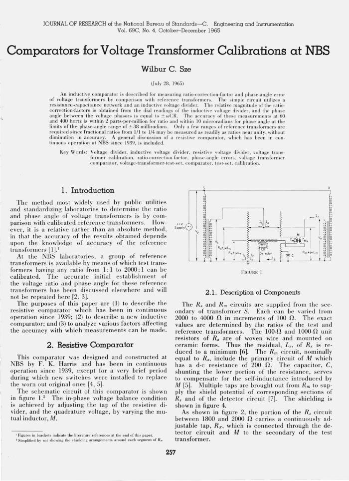
JOURNAL OF RESEARCH of the National Bureau of Standards-C. Engineering and Instrumentation Vol. 69C, No.4, October-December 1965 Comparators for Voltage Transformer Calibrations at NBS Wilbur C. Sze (.Jul y 28, 1965) An indu ctive co mparat or is d esc r ib ed for measuring ra ti o-corr ec tion·fac tor and pha se· angle error of voltage transform ers by com parison with referen ce tr ans former s. Th e s im ple circuit utilizes a r es is tan ce-ca pacit ance ne twork and an in duc ti ve vo ltage divide r. Th e relative magnitud e of the ra ti o· co rr ection·fac tor s is o btain ed from the dial readings of the inductive vo ltage divider, and the phas e angle betw ee n th e voltage ph asors is e qu al to ± wC R. The acc ur acy of th ese measur eme nts at 60 and 400 he rtz is within 2 parts-per-m illion for ra ti o and within 10 mi c roradian s for pha se angle at the limits of the pha se·angle range of ± 38 milliradians. O nl y a few ranges of r eference tran sformers are required sin ce fractional rati os from 1/1 to 1/4 may be mea s ur ed as r ea dil y as ratios nea r unit y, without diminution in accuracy. A ge neral discussion of a r esistive co mp ar at or, which has bee n in con· tinuous operation at NBS sin ce 1939, is includ ed. Key Words: Voltage divider, inductive vo lt age di vider, resistive vo lt age d ivide r, vo lt age tran s· fo rm e r c alibr a ti on, ra ti o·co rr ec tion.factor, pha se· angle e rro rs, vol tage transformer compa ra tor , volt age -tran sformer-t es t ·s et, compa rator, t es t·se t, c alibra ti on. 1. Introduction Th e method most widely use d by public utiliti es and standardizing lab ora tori es to determine the ratio and pha se angle of voltage tr ansformers is by com- parison with ca librat ed reference tran sform ers. How- ever, it is a relative rath er than an absolute method, in that the acc ur acy of the r es ults obtained depe nd s upon the knowledge of accuracy of the referen ce transformers [I].' At th e NBS laboratori es, a group of r efe ren ce transform ers is ava il a ble by mea ns of which tes t trans- form ers having any ratio from 1: 1 to 2000: 1 ca n be c alibrat e d. Th e accurate initial es tablishment of the voltage ratio and pha se angle for th ese reference tran sformers has bee n di sc usse d elsewhere and will not be repea ted here [2 , 3]. The purpos es of this paper are (1) to d esc ribe the r es istive comparator which ha s bee n in co ntinuous operation since 1939; (2) to d esc ribe a new indu ctive comparator; and (3) to analyze various factors affecting the accuracy with which measurements can be made . 2. Resistive Comparator Thi s co mparator was designed and cons tru c te d at NBS by F. K. Harris and ha s bee n in cont inu ous op era tion sin ce 1939, exce pt for a very brief pe riod durin g which new switches were installed to replace the worn out ori gi nal ones [4, 5]. The schema ti c c ircllit of this co mpar ator is shown in figure 1. 2 Th e in-pha se voltage balan ce condition is achieved by adjusting th e tap of the r es istive di- vider, and the quadratur e voltage, by varying th e mu- tual indu c tor , M. I Fi gur es in brackets indi ca te the literatur e references at the end of this pape r. Z Simplifi ed by not showin g Ihe s hi e ldi ng ar rangeme nt s around eac h segment of R •. H.V. Su p pl y Vp F IGURE 1. 2.1. Description of Components Th e Rs and Rm circuits are supplied from the sec - ondary of transform er S. Ea ch ca n be var ied fr om 2000 to 4000 n in inc rement s of 100 n. Th e exact values are determined by the ratios of the t es t and reference transformers. The 100-n and 1000-n unit resistors of Rs are of woven wire and mo unt ed on ceramic forms. Thus the r es idual , Ls, of Rs is r e- duced to a minimum [6]. Th e Rill cir cuit, nominally equal to Rs, includ e the primary circuit of M which has a d·c resistance of 200 n. The c apa citor, C, s huntin g the lower portion of the resistance, se rv es to co mp en sa te for the self-indu ctance int ro du ce d by M [5]. Multiple taps are brought out from Rut to sup- ply th e s hi eld potential of cor r espo nding sec ti ons of Rs and of th e det, ec tor circuit [7]. The shie lding is shown in figure 4. As shown in figure 2, the portion of th e Rs c ircuit between 1800 and 2000 n c arrie s a continuously ad· justable tap , R x, which is connected through th e de- tector circuit and M to the secondary of the test transformer. 257
Transcript of Comparators for voltage transformer calibrations at NBS for Voltage Transformer Calibrations at NBS...
JOURNAL OF RESEARCH of the National Bureau of Standards-C. Engineering and Instrumentation Vol. 69C, No.4, October-December 1965
Comparators for Voltage Transformer Calibrations at NBS Wilbur C. Sze
(.Jul y 28, 1965)
An inductive comparator is desc ribed for measuring ra tio-co rrec tion·fac to r a nd phase·a ngle e rror of voltage transformers by com parison with refe rence tra nsformers. The s im ple c irc uit utili zes a res is tance-capacitance ne twork and a n induc ti ve vo ltage divide r. The re lative magnitude of the ratio· correction·factors is obtained from the dia l readings of the induc tive vo ltage divide r, and the phase angle between the voltage phasors is equal to ± wC R. The acc uracy of these meas urement s at 60 and 400 he rtz is within 2 parts-per-m illion for ra ti o and within 10 microradians for phase a ngle a t the limits of the phase·angl e range of ± 38 milliradians. O nl y a few ranges of refere nce transform e rs a re required s ince fractional ratios from 1/1 to 1/4 may be measured as readil y as ratios nea r unit y, without diminution in accuracy. A general discussion of a resis tive co mpa rator, which has bee n in con· tinuo us operation a t NBS s ince 1939, is included.
Key Words: Voltage divider, induc tive vo ltage di vide r, res istive volt age d ivide r , vo ltage tran s· forme r calibra ti on, ra ti o·correc tion.fac to r, phase·an gle erro rs, voltage t ransform e r compa ra tor, voltage-tran sforme r-tes t·se t , compara tor, tes t·se t , calibra tion .
1. Introduction
The me thod mos t widely used by public utiliti es and sta ndardizing labora tories to de te rmine th e ra tio and phase angle of voltage tra nsform ers is by co mparison with calibrated reference transformers. However, it is a relative rather than a n absolute method, in that the acc uracy of the res ults obtained de pends upon the knowledge of accuracy of the refere nce transformers [I].'
At the NBS laboratories, a group of refere nce transformers is ava ilable by means of whic h test tra nsformers having any ratio from 1: 1 to 2000: 1 can be calibrated. The accurate initial es tabli s hme nt of the voltage ratio and phase angle for these re fere nce transformers has been discussed elsewhere and will not be re peated here [2 , 3].
The purposes of thi s paper are (1) to describe the resistive comparator which has been in continuous operation since 1939; (2) to describe a new inductive comparator; and (3) to analyze various factors affecting the accuracy with which measurements can be made.
2. Resistive Comparator
This comparator was designed and cons truc ted at NBS by F. K. Harris and has been in continuous operation since 1939, except for a ve ry brief pe riod during which new switc hes were in stall ed to replace the worn out original ones [4, 5].
The schematic circ llit of thi s comparator is shown in figure 1.2 The in-phase voltage balance condition is achieved by adjusting the tap of the res istive divider, and the quadrature voltage, by varying the mutual inductor, M.
I Figures in bracket s indica te the literature refe re nces a t the end of thi s pape r. Z Simplified by not showing Ihe s hie lding arrangement s around each segment of R •.
H.V. Su ppl y ~
Vp
F I GURE 1.
2.1 . Description of Components
The Rs and Rm circuits are suppli ed from the secondary of transform er S. Each can be varied from 2000 to 4000 n in increments of 100 n. The exact values are determined by the ratios of the tes t and reference transformers. The 100-n and 1000-n unit resistors of Rs are of woven wire and mounted on ceramic forms. Thus the residual , Ls, of Rs is reduced to a minimum [6]. The Rill circ uit, nominally equal to Rs, include the primary circuit of M which has a d·c resistance of 200 n. The capac itor, C, shunting the lowe r portion of the resistance, serves to compensate for the self-inductance introduced by M [5]. Multiple taps are brought out from Rut to supply the shield potential of corresponding sections of Rs and of the det,ector circuit [7]. The shielding is shown in figure 4.
As shown in figure 2, the portion of the Rs circuit between 1800 and 2000 n carries a continuously ad· justable tap , R x , which is connected through the detector circuit and M to the secondary of the test transformer.
257
IBcon loon 9 X Ion 9 X In
FIGURE 2.
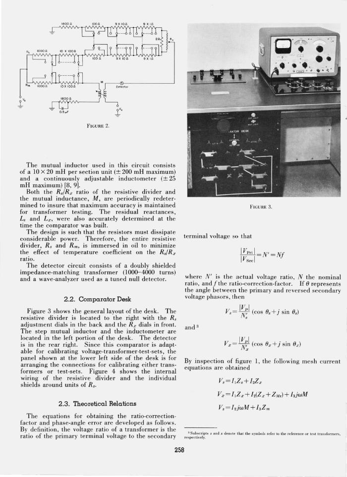
The mutual inductor used in this circuit consists of a 10 X 20 mH per section unit (± 200 mH maximum) and a continuously adjustable inductometer (± 25 mH maximum) [8, 9].
Both the Rs/Rx ratio of the resistive divider and the mutual inductance, M, are periodically redetermined to insure that maximum accuracy is maintained for transformer testing. The residual reactances, Ls and Lx, were also accurately determined at the time the comparator was built.
The design is such that the resistors must dissipate considerable power. Therefore, the entire resistive divider, Rs and R"" is immersed in oil to minimize the effect of temperature coefficient on the Rs/Rx ratio.
The detector circuit consists of a doubly shielded impedance-matching transformer (1000-4000 turns) and a wave-analyzer used as a tuned null detector.
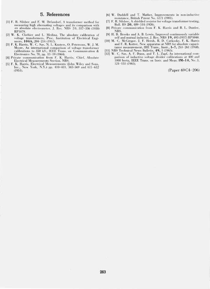
2.2. Comparator Desk
Figure 3 shows the general layout of the desk. The resistive divider is located to the right with the Rs adjustment dials in the back and the Rx dials in front. The step mutual inductor and the inductometer are located in the left portion of the desk. The detector is in the rear right. Since this comparator is adaptable for calibrating voltage-transformer-test-sets, the panel shown at the lower left side of the desk is for arranging the connections for calibrating either transformers or test-sets. Figure 4 shows the internal wiring of the resistive divider and the individual shields around units of Rs.
2.3. Theoretical Relations
The equations for obtaining the ratio-correctionfactor and phase-angle error are developed as follows. By definition, the voltage ratio of a transformer is the ratio of the primary terminal voltage to the secondary
FIGU RE 3.
terminal voltage so that
I Vpri I =N' =Nf IVsec/
where N' is the actual voltage ratio, N the nominal ratio , and f the ratio-correction-factor. If e represents the angle between the primary and reversed secondary voltage phasors, then
V - /Vp/ ( II +. . ll) S - N' cos Us } sm U s
s
V - /Vp/ ( II +. . ll) X - N~ cos u x } sm u x
By inspection of figure 1, the following mesh current equations are obtained
Vs =12jwM + 13Z",
3 Subscripts s and x denote that the symbols refer to the reference or tes t transformers, respectively.
258

F IGU RE 4.
12 = 0 when a null is indicated on the de tector, then
and
Since Zm= R", by the addition of C, and Rm = Rs nominally , the balance equation beco mes
(cos ex+ j sin ex) Nx/ x
and on se paration
(cos Os+ j sin Os) Nsf.
{Rx [1 + jw (L x - Ls + M) ] } Rs Rx Rs Rx
/x = NsRs ( Is cos Ox ) NxRx . (Lx. Ls M)
cos Os- sm esw Rx - Rs + Rx
_ NsRs iF _ ) 1:. ( 2 _ 2) - NxRx+ vs 1 + 2 0s OJ."
and 4
(Lx Ls M) . ex = Os + w Rx - Rs + Rx radIans
As previously indicated, Rs and R", circuits cons titute a burden on the refere nce tran sformer- Therefore, Is and es are determined with these burdens _
The design of the divider is such that the balance conditions require
thi s requireme nt is met by using reference transformers whose voltage ratios have been adjusted to values 2 percent less than the integral values usually enc ounte r ed as nominal r a tios In in s trum e nt transform ers.
The minimum resolution of thi s setup is s uc h that the precision for ratio meas ure ments is 2 ppm and for phase angle, 15 w ad at 25 and 60 Hz. However, susce ptibility of the mutual inductor to the gradients of s tray magnetic fi elds, large residuals and uncertainty in ratio calibration of the resis tive divider limit the accuracy of these measurements to 10 ppm and 60 ILrad, res pec tively. These errors increase rapidly with freque ncy. Therefore, this comparator is not s uitable for accurate calibrations beyond 60 Hz.
3. Inductive Comparator
This comparator avoids a number of the objec tionable features of the resistive comparator- The shielding is simple and is easily accomplished ; the method is capable of exte nsion to co ver the audio-freque ncy range; the apparatus is less bulky and requires ver y little power for operation; the co mpone nts are in herently more accurate and s table and readily available commercially; the r atio difference is indicated directly on the decade di als; and the set (except the detector) is self-contained in one portable case .
The schemati c diagram of the circ uit is shown in figure 5, which indicates the positions of resis tor , R, and detector when the voltage phasor of the tes t transformer , X , leads that of the refere nce transformer , S . For lagging angles, the positions of R and detector are
4 The (f,- I) a nd Os for the NBS re ference tntn S fO I~ll e rs a re ve r y small. The refore. t he approximations Illade a re justifi able.
H.V. ~ Vp Supply
FIGURE 5.
259

simply interchanged. The in-phase voltage balance is obtained by adjusting the tap on the inductive voltage divider, and the quadrature voltage balance is obtained by adjusting either the resistor or the capacitor.
3.1. Theoretical Relations
As previously defined, the voltage ratio is
and
IVPri I =N' =Nf. IVsecl '
v. - IVpl ( e +. . e) s-Ns/s cos s jsm s,
V - IVpl . . v~ X-N-j (cos ex+j sm ex)=-'
x x m
m being the actual ratio of the inductive voltage divider. Corrections to the ratios and the phase angles of the inductive voltage divider used are insignificant and can be neglected. Then from figure 5,
Vs _ 1 - jwCR _ 1 2C2R2 . CR V~ -1+w2C2R2 - -w -jW
The balance equation of the circuit becomes
N x/x( cos es + j sin es) mNs/s(cos ex + j sin ex)
and on separation and by neglecting second order terms
radians, and
I x= mNs/s (GOS ex -w2c2R2+ wCR sin ex.) Nx cos es
For relative lagging phase angle, with the detector and resistor, R, interchanged,
3.2. Loading Effects
S ince th e input impedance of the inductive voltage divider a t 60 Hz is in excess of 0.8 Mfl (nearly 1.00
power factor), the effect of loading of the I x and ex of the test transformer can be expressed as
( Equivalent Total Impedance Referred) to Transformer Secondary
(External Impedance)
= (Correction to Ix and ex).
A transformer with an equivalent resistance of 1 fl (which is easily measurable) will result in a correction of approximately 1 ppm [5].
The effect of loading by the quadrature balancing network on either the inductive voltage divider or the reference transformer is usually insignificant. At the limits of phase-angle range of:::t: 37.8 mrad (130 min), the correction to ratio and phase angle of the inductive voltage divider is - 1 ppm and < 4 ILrad, respectively; or, to the reference transformer, < < 1 ppm and < < 1 ILrad.
3.3. Description of Components
All the components in this circuit are readily available commercially or accessible in most testing laboratories. In figure 5, R is a 0-10 kfl, lO-turn, continuously adjustable resistor with small residual reactance. C is a 10 X 1 nF decade capacitor with a dissipation factor of < 0.0003. Both Rand C were calibrated before and after assembly. The deviations from nominal values were found to be within 5 fl and 5 pF, respectively.
The inductive voltage divider is a six· decade unit designed for optimum performance at 60 Hz.5 For tests at higher frequencies (up to 1 kHz), it can easily be replaced by a unit of appropriate design, or by application of appropriate loading corrections to the ratio·correction-factor and phase angle. However, due to the simplicity of the circuitry and infrequent requests for calibrations at higher frequencies , a tem-
S S ince maximum voltage on this divider is limited 10 ISO V at 60 Hz, it must be connec ted across the test transformer rather than the reference transforme r whose secondary voltage may exceed thi s value in some instances.
21k II 0-150 VOLTS
Detector
FIGURE 6.
V, .g,.
Fuse
In duct ive Voltage Divider
260

I ·
FIGU RE 7.
porary setup is generally used at NBS. This consis ts of a high fre quency divider, commercially available air capacitors, and an a·c decade resis tor.
The input impedance of the inductive voltage di· vider was measured in a capacitive voltage divider setup; see fi gure 7 for circ uit diagram [10]. The voltage-ratio corrections and phase-angle errors were obtained by a tracking method [11]. However , for a well designed induc ti ve voltage di vider , these corrections are u sually < 0.2 ppm of input in ratio linearity deviation and < 8 fLrad of input in phase deviation.
The detector circuit consists of a wave-analyzer used as a tuned null indicator and a specially cons tructed shielded transformer, shown in fi gure 6. Thi s transformer is used to matc h impedances and to isolate the meas uring c irc uit from the detector circuit elec trostatically. It consis ts of a high permeability toroid al core, a 700-tWll inner prim ary windin g, two elec tros ta ti c shields, a 3500-turn outer secondary winding, and an overall Mu-me tal case. The use of a toroid minimizes the magneti c pickup from s tray fields in the laboratory.
The polarit y checking volLmeter is a 0-150 V, 3-in. panel-type in s trume nt of 3 percent acc uracy. The 21 kfl resistor matc hes its internal resis tance. The voltmeter indicates the secondary voltage of the tes t transform er wh e n th e selec tor s witc h i s in th e "CALIBRATION" position.
Figures 8 and 9 show the exterior and interior of the comparator. The cylindrical shield shown III
the interior view encloses the lO-kfl resistor.
3.4. Accuracy Determination
Mter the completion of the comparator , the calibration of ea c h component was rechecked.
The accuracy of the completed co mparator was verified by the following procedures : (1) connecting a single voltage so urce to both "Vs" and "Vx" terminals to obta in the zero corrections for C and Rand the unity co rrec tion for dial se ttings of the inductive voltage divide r; (2) calibrating several pairs of transformers of the same ratio to reference transformers of appropriate r a tios, thus determining the relative ratiocorrection-fac tors and phase-angle errors with several values of secondary burden for each pair of transform-
261
784-6570- 65-2
FI GU RE 8.
F IGU RE 9.

ers; (3) co mparing each pair of these calibrated transformers to each other with the comparator alternately as reference and test units and with various combinations of previously used secondary burdens; and (4) co nnec ting a single voltage source to "Vx " terminals and to the input of a calibrated inductive voltage divider, whose output is connected to "Vs" terminals in order to check the fractional ratio measurements_
3.5. Transformer Testing Procedure
A reference transformer is selected so that Ns ;?!: N xThe selector switch is set to "CHE CK" position; and the ratio, m, is set to equal Nx/Ns. The secondaries of the test and reference transformers are connected to "Vx " and "Vs" terminals respectively. With the transformers energized and the voltmeter switch depressed, the voltmeter indicates (VS - Vx )/2 if the polarities of Vs and Vx are correctly connected to the comparator. [The polarity of Vx must be reversed if voltmeter indicates (VS + Vx )/2.] The test proceeds with the selector switch turned to " CALIBRATION." Vx is now indicated on the voltmeter.
If Nx > Ns by more than 10 percent, the test can still be made, but the reference transformer must be connected to "Vx " terminal and the test transformer to "Vs". At the balanced condition, the ratio, m, will indicate the reciprocal of the relative ratio-correctionfactors, and the relative phase-angle switch will show the negative of the markings as shown in figures 6 and 8.
3.6. Consideration of Errors
An examination of errors requires a careful appraisal of all components of the measuring circuit as well as a justification of estimations, even though in this case one would expect most of the associated errors to be negligible.
The first to be considered are those possible errors concealed through approximation in developing the e xpressions for obtaining the ratio-correction-factor and phase-angle relations, where the effects of the residual of the lO-kD resistor and the dissipation factor of the decade capacitor are ignored. Approximate magnitudes of these errors can be obtained by adding the es timated equivalent residual reactance across R and es timated equivalent series resistance to C. These effects were found to be less than 0.5 ppm for ratio and 5 ILrad for phase angle at the limits of the phase angle range (± 38 mrad) at 60 Hz.
A second source of uncertainty is in the calibration of the inductive voltage dividers. However, past experience indicates that errors should not exceed 0.2 ppm of input in ratio linearity deviation and 2 ILrad of input in phase deviation [121-
Errors caused by the leads, switch contacts, and imperfect shields are estimated to be < 0.5 ppm and < 2 ILrad.
The last important uncertainty that should be considered is in obtaining the transformer secondary
load corrections. Such errors are estimated to be 0.5 ppm and 3 ILrad for each transformer.
Finally, one should add 3 times the standard deviations (0.3 ppm of ratio and 1 ILrad) of the results obtained in repeated balances of the comparator to the combination of the systematic-error estimates.
Uncertainties to Uncertainties ratio-correction- to phase
factor angles Source of errors
n n' n n'
ppm wad From assumptions made in
equations 0.5 0.25 5 25 Calibration of the inductive
voltage divider .2 .04 2 4 Obtaining secondary load cor-
rections (S) .5 .25 3 9 Obtaining secondary' load cor-
rections (X) .5 .25 3 9 Leads and contacts .5 .25 2 4
- -
~n' 1.04 51 (~n')I /' 1.02 7.1 3 X standard deviations 0.90 3.0
---Maximum error 1.9 ppm 10.1 J-Lrad
4. Conclusion
A high accuracy inductive comparator has been developed for measuring the relative voltage ratio and phase angle of voltage transformers and testing sets at power and audio frequencies. An overall accuracy of < 2 ppm in ratio measurements 1lnd < 10 ILrad in phase angle at 60 and 400 Hz is achieved, with a slight reduction in the accuracy attainable at higher audio frequencies.
The simple circuit does not require any special equipment. Only a few ranges of reference transformers are required , since fractional ratios from 1/1 to 1/4 may be measured as readily as ratios near unity .
This inductive comparator could replace testing sets now in general use. It is compact and portable, has a broader useful frequency range, and exceeds the accuracy of many commercial sets presently available by one or two orders of magni tude.
The resistive comparator will continue to be used at NBS for calibration of voltage transformers at 25 Hz at which frequency the operating voltage is usually above the maximum operating voltage of the inductive comparator.
The author acknowledges the valuable help and advice received from Mr. F. L. Hermach, Chief, Electrical Instrument Section, NBS. Mr. R. J. Berry contributed skillfully III constructing the new comparator.
262
, I
5. References
[1) F. B. Silsbee and F. M. Defandorf, A transform er method for measuring high alternating voltages and its comparison with an abso lute elec trometer, J. Res. NBS 20,317- 336 (1938) RPI079.
[2) W. K. Clothier and L. Medina, The absolute calibration of vo ltage transform ers, Proc. J nst itution of Elec trica l Engineers, 104A, 204- 214 (1957).
[3) F. K. Harri s, W. C. Sze, N. L. Kusters, O. P ete rsons, W. J. M. Moore, An international comparison of voltage transform er calibrations to 350 kV, IEEE Trans. on Communication & Electronics No. 70, pp_ l3- 19 (1964).
[4) Private co mmunication from F. K. Harri s, Chief, Absolute Electrical Measurements Section, NBS.
[5) F. K. Harris, Electrical Measurements (John Wiley and Sons, Inc. , New York, N.Y.) pp. 410-411, 565-569 and 611-612 (1951).
[6) W. Duddell and T. Mather, Improvements in non-inductive res is tance, British Patent No. 5171 (1901).
[7J F. B. Si lsbee, A shie lded res istor for voltage transformer testing, Bull. BS 20,489-514 (1926).
[8) Private co mmunica tion from F. K. Harri s and B. L. Dunfee, NBS .
[9) H. B. Brooks and A. B. Lewis , Improved continuously variable se lf and mutual inductor, 1. Res . NBS 19,493 (1937) RP1040.
[10) M. C. McGregor, J. F. Hersh, R. D. Cutkosky, F. K. Harris anil F. R. Kotter, New apparatus at NBS for abso lute capaci· tance measurement, IRE Trans. , Instr., 1-7, 253-261 (1958).
[11) NBS Technical News Bulletin, 49, 1 (1965). [12) W. C. Sze, A. F. Dunn, and T. L. Zapf, An international com
parison of inductive voltage divider calibrations at 400 ann 1000 hertz, IEEE Trans. on Instr. and Meas . IM-14 , No.3, 124- 131 (1965).
(Paper 69 C4-206)
263