Comparative Analysis Of Master-Slave Latches And Flip ... · PDF fileComparative Analysis of...
13
536 IEEE JOURNAL OF SOLID-STATE CIRCUITS, VOL. 34, NO. 4, APRIL 1999 Comparative Analysis of Master–Slave Latches and Flip-Flops for High-Performance and Low-Power Systems Vladimir Stojanovic and Vojin G. Oklobdzija, Fellow, IEEE Abstract—In this paper, we propose a set of rules for consistent estimation of the real performance and power features of the flip-flop and master–slave latch structures. A new simulation and optimization approach is presented, targeting both high- performance and power budget issues. The analysis approach reveals the sources of performance and power-consumption bot- tlenecks in different design styles. Certain misleading parameters have been properly modified and weighted to reflect the real properties of the compared structures. Furthermore, the results of the comparison of representative master–slave latches and flip- flops illustrate the advantages of our approach and the suitability of different design styles for high-performance and low-power applications. I. INTRODUCTION I NTERPRETATION of published results comparing various latches and flip-flops has been very difficult because of the use of different simulation methods for their generation and presentation. In this paper, we establish a set of rules with the goal of making the comparisons fair and realistic. Simulation of the latches and flip-flops obtained by using different design styles makes this analysis more difficult in trying to achieve consistent and comparable results. There are two major results produced in the course of this work: 1) definition of the relevant set of parameters to be mea- sured and rules for weighting their importance; 2) a set of relevant simulation conditions, which emphasize the parameters of interest. The simulation and optimization procedures have high perfor- mance as the primary goal, but we have also paid attention to the possible reductions in power consumption, given that the limitation in performance is usually imposed by the available power budget. II. ANALYSIS A. Power Considerations Power consumption of a circuit depends strongly on its structure and the statistics of the applied data. Thus, power measurements should be conducted for the range of different data patterns comprising the worst and the best cases. Our goal is not only to find the range of power consumption for Manuscript received April 10, 1998; revised October 15, 1998. V. Stojanovic is with the Faculty of Electrical Engineering, University of Belgrade, Serbia, Yugoslavia. V. G. Oklobdzija is with Integration Corp., Berkeley, CA 94708 USA (e- mail: [email protected]). Publisher Item Identifier S 0018-9200(99)02434-8. Fig. 1. The pseudorandom sequence. all the possible cases but also to define special patterns that are to reveal the major sources of power dissipation for the given family of master–slave latches and flip-flops (for specific applications where the statistics of data is known in advance, like in data processing, it is desirable to optimize the structure for the given data distribution). In our simulation, the data activity rate presents the average number of output transitions per clock cycle. We have applied four different data sequences where ...010 101 010..., reflects the maximum internal dynamic power con- sumption. However, depending on the structure, the sequence ...111 111... can in some cases dissipate more power. In general, a pseudorandom sequence with equal probability of all transitions (data activity rate ) is considered to reflect the average internal power consumption given the uniform data distribution; see Fig. 1. The sequence ...111 111 111..., reflects the power dissipation of precharged nodes. The sequence ...000 000 000..., reflects minimum power consumption. Depending on the size of the precharged and static parts, internal dynamic power consumption can be estimated based on the analysis of Fig. 2. The starting point is a well-known formula for estimation of dynamic power consumption where where switching probability of node (in regard to the clock cycle); swing range coefficient of node ( for rail- to-rail swing); total capacitance of node ; clock frequency; rail-to-rail voltage range (supply voltage). This strategy has been generalized in Fig. 2 to describe the differences in switching activity, and therefore power con- sumption, for different design styles. Capacitances and are calculated from node to node in the given topology taking into account the and coefficient of each node in the circuit. This 0018–9200/99$10.00 1999 IEEE
Transcript of Comparative Analysis Of Master-Slave Latches And Flip ... · PDF fileComparative Analysis of...
536 IEEE JOURNAL OF SOLID-STATE CIRCUITS, VOL. 34, NO. 4, APRIL 1999
Comparative Analysis of Master–SlaveLatches and Flip-Flops for
High-Performance and Low-Power SystemsVladimir Stojanovic and Vojin G. Oklobdzija,Fellow, IEEE
Abstract—In this paper, we propose a set of rules for consistentestimation of the real performance and power features of theflip-flop and master–slave latch structures. A new simulationand optimization approach is presented, targeting both high-performance and power budget issues. The analysis approachreveals the sources of performance and power-consumption bot-tlenecks in different design styles. Certain misleading parametershave been properly modified and weighted to reflect the realproperties of the compared structures. Furthermore, the resultsof the comparison of representative master–slave latches and flip-flops illustrate the advantages of our approach and the suitabilityof different design styles for high-performance and low-powerapplications.
I. INTRODUCTION
I NTERPRETATION of published results comparing variouslatches and flip-flops has been very difficult because of the
use of different simulation methods for their generation andpresentation. In this paper, we establish a set of rules with thegoal of making the comparisons fair and realistic. Simulationof the latches and flip-flops obtained by using different designstyles makes this analysis more difficult in trying to achieveconsistent and comparable results. There are two major resultsproduced in the course of this work:
1) definition of the relevant set of parameters to be mea-sured and rules for weighting their importance;
2) a set of relevant simulation conditions, which emphasizethe parameters of interest.
The simulation and optimization procedures have high perfor-mance as the primary goal, but we have also paid attention tothe possible reductions in power consumption, given that thelimitation in performance is usually imposed by the availablepower budget.
II. A NALYSIS
A. Power Considerations
Power consumption of a circuit depends strongly on itsstructure and the statistics of the applied data. Thus, powermeasurements should be conducted for the range of differentdata patterns comprising the worst and the best cases. Ourgoal is not only to find the range of power consumption for
Manuscript received April 10, 1998; revised October 15, 1998.V. Stojanovic is with the Faculty of Electrical Engineering, University of
Belgrade, Serbia, Yugoslavia.V. G. Oklobdzija is with Integration Corp., Berkeley, CA 94708 USA (e-
mail: [email protected]).Publisher Item Identifier S 0018-9200(99)02434-8.
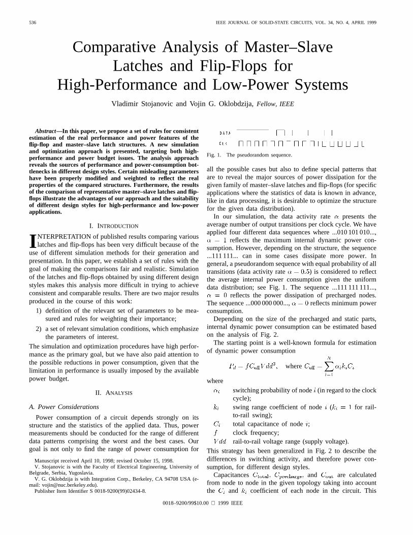
Fig. 1. The pseudorandom sequence.
all the possible cases but also to define special patterns thatare to reveal the major sources of power dissipation for thegiven family of master–slave latches and flip-flops (for specificapplications where the statistics of data is known in advance,like in data processing, it is desirable to optimize the structurefor the given data distribution).
In our simulation, the data activity rate presents theaverage number of output transitions per clock cycle. We haveapplied four different data sequences where ...010 101 010...,
reflects the maximum internal dynamic power con-sumption. However, depending on the structure, the sequence...111 111... can in some cases dissipate more power. Ingeneral, a pseudorandom sequence with equal probability of alltransitions (data activity rate ) is considered to reflectthe average internal power consumption given the uniformdata distribution; see Fig. 1. The sequence ...111 111 111...,
reflects the power dissipation of precharged nodes.The sequence ...000 000 000..., reflects minimum powerconsumption.
Depending on the size of the precharged and static parts,internal dynamic power consumption can be estimated basedon the analysis of Fig. 2.
The starting point is a well-known formula for estimationof dynamic power consumption
where
where
switching probability of node (in regard to the clockcycle);swing range coefficient of node( for rail-to-rail swing);total capacitance of node;clock frequency;rail-to-rail voltage range (supply voltage).
This strategy has been generalized in Fig. 2 to describe thedifferences in switching activity, and therefore power con-sumption, for different design styles.
Capacitances and are calculatedfrom node to node in the given topology taking into accountthe and coefficient of each node in the circuit. This
0018–9200/99$10.00 1999 IEEE
STOJANOVIC AND OKLOBDZIJA: MASTER–SLAVE AND FLIP-FLOP LATCHES 537
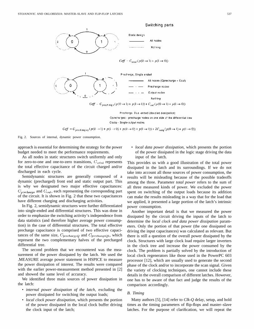
Fig. 2. Sources of internal, dynamic power consumption.
approach is essential for determining the strategy for the powerbudget needed to meet the performance requirements.
As all nodes in static structures switch uniformly and onlyfor zero-to-one and one-to-zero transitions, representsthe total effective capacitance of the circuit charged and/ordischarged in each cycle.
Semidynamic structures are generally composed of adynamic (precharged) front end and static output part. Thisis why we designated two major effective capacitances:
and , each representing the corresponding partof the circuit. It is shown in Fig. 2 that these two capacitanceshave different charging and discharging activities.
In Fig. 2, semidynamic structures were further differentiatedinto single-ended and differential structures. This was done inorder to emphasize the switching activity’s independence fromdata statistics (and therefore higher average power consump-tion) in the case of differential structures. The total effectiveprecharge capacitance is comprised of two effective capaci-tances of the same size, and , whichrepresent the two complementary halves of the prechargeddifferential tree.
The second problem that we encountered was the mea-surement of the power dissipated by the latch. We used the.MEASURE average power statement in HSPICE to measurethe power dissipation of interest. The results were comparedwith the earlier power-measurement method presented in [2]and showed the same level of accuracy.
We identified three main sources of power dissipation inthe latch:
• internal power dissipation of the latch,excluding thepower dissipated for switching the output loads;
• local clock power dissipation,which presents the portionof the power dissipated in the local clock buffer drivingthe clock input of the latch;
• local data power dissipation,which presents the portionof the power dissipated in the logic stage driving the datainput of the latch.
This provides us with a good illustration of the total powerdissipated in the latch and its surroundings. If we do nottake into account all those sources of power consumption, theresults will be misleading because of the possible tradeoffsamong the three. Parametertotal power refers to the sum ofall three measured kinds of power. We excluded the powerspent on switching of the output loads because its additioncan make the results misleading in a way that for the load thatwe applied, it presented a large portion of the latch’s intrinsicpower consumption.
Another important detail is that we measured the powerdissipated by the circuit driving the inputs of the latch todetermine thelocal clock and data power dissipationparam-eters. Only the portion of that power (the one dissipated ondriving the input capacitances) was calculated as relevant. Butthere is still a question of the overall power dissipated by theclock. Structures with large clock load require larger invertersin the clock tree and increase the power consumed by theclock. The problem is partially solved by the introduction oflocal clock regenerators like those used in the PowerPC 603processor [12], which are usually used to generate the secondphase of the clock and/or to incorporate the scan signal. Giventhe variety of clocking techniques, one cannot include thesedetails in the overall comparison of different latches. However,one has to be aware of that fact and judge the results of thecomparison accordingly.
B. Timing
Many authors [5], [14] refer toClk-Q delay, setup, and holdtimes as the timing parameters of flip-flops and master–slavelatches. For the purpose of clarification, we will repeat the
538 IEEE JOURNAL OF SOLID-STATE CIRCUITS, VOL. 34, NO. 4, APRIL 1999
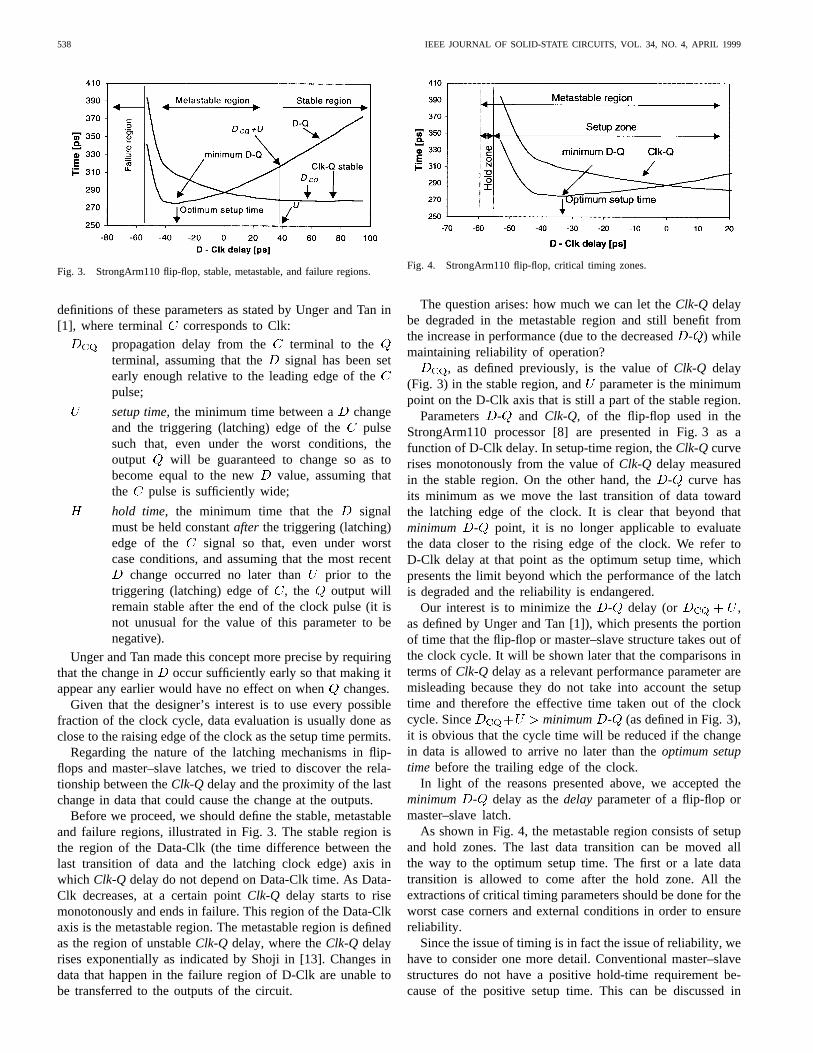
Fig. 3. StrongArm110 flip-flop, stable, metastable, and failure regions.
definitions of these parameters as stated by Unger and Tan in[1], where terminal corresponds to Clk:
propagation delay from the terminal to theterminal, assuming that the signal has been setearly enough relative to the leading edge of thepulse;
setup time,the minimum time between a changeand the triggering (latching) edge of the pulsesuch that, even under the worst conditions, theoutput will be guaranteed to change so as tobecome equal to the new value, assuming thatthe pulse is sufficiently wide;
hold time, the minimum time that the signalmust be held constantafter the triggering (latching)edge of the signal so that, even under worstcase conditions, and assuming that the most recent
change occurred no later than prior to thetriggering (latching) edge of , the output willremain stable after the end of the clock pulse (it isnot unusual for the value of this parameter to benegative).
Unger and Tan made this concept more precise by requiringthat the change in occur sufficiently early so that making itappear any earlier would have no effect on whenchanges.
Given that the designer’s interest is to use every possiblefraction of the clock cycle, data evaluation is usually done asclose to the raising edge of the clock as the setup time permits.
Regarding the nature of the latching mechanisms in flip-flops and master–slave latches, we tried to discover the rela-tionship between theClk-Q delay and the proximity of the lastchange in data that could cause the change at the outputs.
Before we proceed, we should define the stable, metastableand failure regions, illustrated in Fig. 3. The stable region isthe region of the Data-Clk (the time difference between thelast transition of data and the latching clock edge) axis inwhich Clk-Q delay do not depend on Data-Clk time. As Data-Clk decreases, at a certain pointClk-Q delay starts to risemonotonously and ends in failure. This region of the Data-Clkaxis is the metastable region. The metastable region is definedas the region of unstableClk-Q delay, where theClk-Q delayrises exponentially as indicated by Shoji in [13]. Changes indata that happen in the failure region of D-Clk are unable tobe transferred to the outputs of the circuit.
Fig. 4. StrongArm110 flip-flop, critical timing zones.
The question arises: how much we can let theClk-Q delaybe degraded in the metastable region and still benefit fromthe increase in performance (due to the decreased- ) whilemaintaining reliability of operation?
, as defined previously, is the value ofClk-Q delay(Fig. 3) in the stable region, and parameter is the minimumpoint on the D-Clk axis that is still a part of the stable region.
Parameters - and Clk-Q, of the flip-flop used in theStrongArm110 processor [8] are presented in Fig. 3 as afunction of D-Clk delay. In setup-time region, theClk-Q curverises monotonously from the value ofClk-Q delay measuredin the stable region. On the other hand, the- curve hasits minimum as we move the last transition of data towardthe latching edge of the clock. It is clear that beyond thatminimum - point, it is no longer applicable to evaluatethe data closer to the rising edge of the clock. We refer toD-Clk delay at that point as the optimum setup time, whichpresents the limit beyond which the performance of the latchis degraded and the reliability is endangered.
Our interest is to minimize the - delay (or ,as defined by Unger and Tan [1]), which presents the portionof time that the flip-flop or master–slave structure takes out ofthe clock cycle. It will be shown later that the comparisons interms ofClk-Q delay as a relevant performance parameter aremisleading because they do not take into account the setuptime and therefore the effective time taken out of the clockcycle. Since minimum - (as defined in Fig. 3),it is obvious that the cycle time will be reduced if the changein data is allowed to arrive no later than theoptimum setuptime before the trailing edge of the clock.
In light of the reasons presented above, we accepted theminimum - delay as thedelay parameter of a flip-flop ormaster–slave latch.
As shown in Fig. 4, the metastable region consists of setupand hold zones. The last data transition can be moved allthe way to the optimum setup time. The first or a late datatransition is allowed to come after the hold zone. All theextractions of critical timing parameters should be done for theworst case corners and external conditions in order to ensurereliability.
Since the issue of timing is in fact the issue of reliability, wehave to consider one more detail. Conventional master–slavestructures do not have a positive hold-time requirement be-cause of the positive setup time. This can be discussed in
STOJANOVIC AND OKLOBDZIJA: MASTER–SLAVE AND FLIP-FLOP LATCHES 539
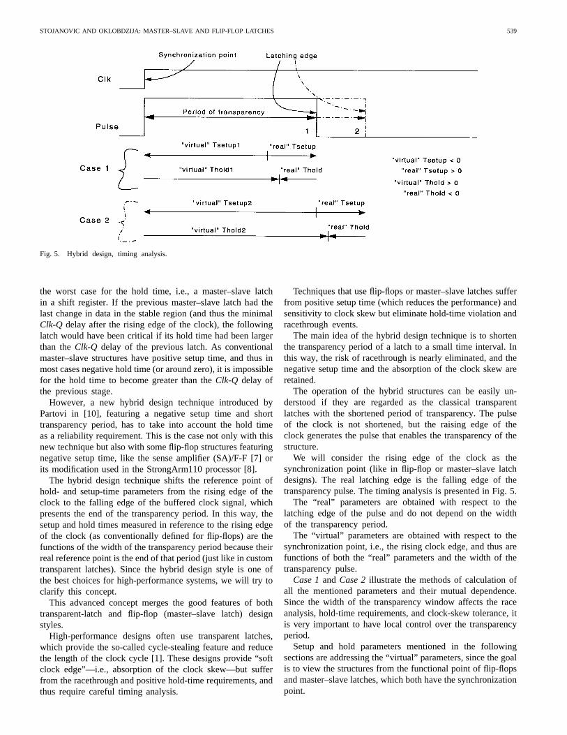
Fig. 5. Hybrid design, timing analysis.
the worst case for the hold time, i.e., a master–slave latchin a shift register. If the previous master–slave latch had thelast change in data in the stable region (and thus the minimalClk-Q delay after the rising edge of the clock), the followinglatch would have been critical if its hold time had been largerthan theClk-Q delay of the previous latch. As conventionalmaster–slave structures have positive setup time, and thus inmost cases negative hold time (or around zero), it is impossiblefor the hold time to become greater than theClk-Q delay ofthe previous stage.
However, a new hybrid design technique introduced byPartovi in [10], featuring a negative setup time and shorttransparency period, has to take into account the hold timeas a reliability requirement. This is the case not only with thisnew technique but also with some flip-flop structures featuringnegative setup time, like the sense amplifier (SA)/F-F [7] orits modification used in the StrongArm110 processor [8].
The hybrid design technique shifts the reference point ofhold- and setup-time parameters from the rising edge of theclock to the falling edge of the buffered clock signal, whichpresents the end of the transparency period. In this way, thesetup and hold times measured in reference to the rising edgeof the clock (as conventionally defined for flip-flops) are thefunctions of the width of the transparency period because theirreal reference point is the end of that period (just like in customtransparent latches). Since the hybrid design style is one ofthe best choices for high-performance systems, we will try toclarify this concept.
This advanced concept merges the good features of bothtransparent-latch and flip-flop (master–slave latch) designstyles.
High-performance designs often use transparent latches,which provide the so-called cycle-stealing feature and reducethe length of the clock cycle [1]. These designs provide “softclock edge”—i.e., absorption of the clock skew—but sufferfrom the racethrough and positive hold-time requirements, andthus require careful timing analysis.
Techniques that use flip-flops or master–slave latches sufferfrom positive setup time (which reduces the performance) andsensitivity to clock skew but eliminate hold-time violation andracethrough events.
The main idea of the hybrid design technique is to shortenthe transparency period of a latch to a small time interval. Inthis way, the risk of racethrough is nearly eliminated, and thenegative setup time and the absorption of the clock skew areretained.
The operation of the hybrid structures can be easily un-derstood if they are regarded as the classical transparentlatches with the shortened period of transparency. The pulseof the clock is not shortened, but the raising edge of theclock generates the pulse that enables the transparency of thestructure.
We will consider the rising edge of the clock as thesynchronization point (like in flip-flop or master–slave latchdesigns). The real latching edge is the falling edge of thetransparency pulse. The timing analysis is presented in Fig. 5.
The “real” parameters are obtained with respect to thelatching edge of the pulse and do not depend on the widthof the transparency period.
The “virtual” parameters are obtained with respect to thesynchronization point, i.e., the rising clock edge, and thus arefunctions of both the “real” parameters and the width of thetransparency pulse.
Case 1and Case 2illustrate the methods of calculation ofall the mentioned parameters and their mutual dependence.Since the width of the transparency window affects the raceanalysis, hold-time requirements, and clock-skew tolerance, itis very important to have local control over the transparencyperiod.
Setup and hold parameters mentioned in the followingsections are addressing the “virtual” parameters, since the goalis to view the structures from the functional point of flip-flopsand master–slave latches, which both have the synchronizationpoint.
540 IEEE JOURNAL OF SOLID-STATE CIRCUITS, VOL. 34, NO. 4, APRIL 1999
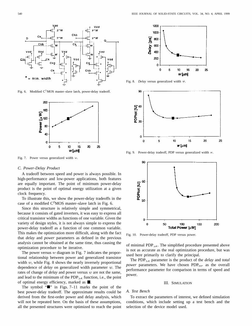
Fig. 6. Modified C2MOS master–slave latch, power-delay tradeoff.
Fig. 7. Power versus generalized widthw.
C. Power-Delay Product
A tradeoff between speed and power is always possible. Inhigh-performance and low-power applications, both featuresare equally important. The point of minimum power-delayproduct is the point of optimal energy utilization at a givenclock frequency.
To illustrate this, we show the power-delay tradeoffs in thecase of a modified CMOS master–slave latch in Fig. 6.
Since this structure is relatively simple and symmetrical,because it consists of gated inverters, it was easy to express allcritical transistor widths as functions of one variable. Given thevariety of design styles, it is not always simple to express thepower-delay tradeoff as a function of one common variable.This makes the optimization more difficult, along with the factthat delay and power parameters as defined in the previousanalysis cannot be obtained at the same time, thus causing theoptimization procedure to be iterative.
The power versus diagram in Fig. 7 indicates the propor-tional relationship between power and generalized transistorwidth , while Fig. 8 shows the nearly inversely proportionaldependence ofdelay on generalized width parameter. Therates of change ofdelayand power versus are not the same,and lead to the minimum of the PDPfunction, i.e., the pointof optimal energy efficiency, marked as.
The symbol “ ” in Figs. 7–11 marks the point of thebest power-delay tradeoff. The approximate results could bederived from the first-order power and delay analysis, whichwill not be repeated here. On the basis of these assumptions,all the presented structures were optimized to reach the point
Fig. 8. Delay versus generalized widthw.
Fig. 9. Power-delay tradeoff, PDP versus generalized widthw.
Fig. 10. Power-delay tradeoff, PDP versus power.
of minimal PDP . The simplified procedure presented aboveis not as accurate as the real optimization procedure, but wasused here primarily to clarify the principal.
The PDP parameter is the product of thedelayand totalpower parameters. We have chosen PDPas the overallperformance parameter for comparison in terms of speed andpower.
III. SIMULATION
A. Test Bench
To extract the parameters of interest, we defined simulationconditions, which include setting up a test bench and theselection of the device model used.
STOJANOVIC AND OKLOBDZIJA: MASTER–SLAVE AND FLIP-FLOP LATCHES 541
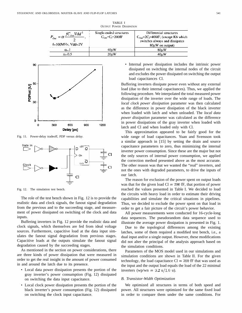
TABLE IOUTPUT POWER DISSIPATION
Fig. 11. Power-delay tradeoff, PDP versusdelay.
Fig. 12. The simulation test bench.
The role of the test bench shown in Fig. 12 is to provide therealistic data and clock signals, the fanout signal degradationfrom the previous and to the succeeding stage, and measure-ment of power dissipated on switching of the clock and datainputs.
Buffering inverters in Fig. 12 provide the realistic data andclock signals, which themselves are fed from ideal voltagesources. Furthermore, capacitive load at the data input sim-ulates the fanout signal degradation from previous stages.Capacitive loads at the outputs simulate the fanout signaldegradation caused by the succeeding stages.
As mentioned in the section on power considerations, thereare three kinds of power dissipation that were measured inorder to get the real insight in the amount of power consumedin and around the latch due to its presence.
• Local data power dissipation presents the portion of thegray inverter’s power consumption (Fig. 12) dissipatedon switching the data input capacitance.
• Local clock power dissipation presents the portion of theblack inverter’s power consumption (Fig. 12) dissipatedon switching the clock input capacitance.
• Internal power dissipation includes the intrinsic powerdissipated on switching the internal nodes of the circuitand excludes the power dissipated on switching the outputload capacitances Cl.
Buffering inverters dissipate power even without any externalload (due to their internal capacitances). Thus, we applied thefollowing procedure. We interpolated the total measured powerdissipation of the inverter over the wide range of loads. Thelocal clock power dissipationparameter was then calculatedas the difference in power dissipation of the black inverterwhen loaded with latch and when unloaded. Thelocal datapower dissipationparameter was calculated as the differencein power dissipations of the gray inverter when loaded withlatch and Cl and when loaded only with Cl.
This approximation appeared to be fairly good for thewide range of load capacitances. Yuan and Svensson tooka similar approach in [15] by setting the drain and sourcecapacitance parameters to zero, thus minimizing the internalinverter power consumption. Since these are the major but notthe only sources of internal power consumption, we appliedthe correction method presented above as the most accurate.The other reason was that we wanted the “real” inverters, andnot the ones with degraded parameters, to drive the inputs ofour latch.
The reason for exclusion of the power spent on output loadswas that for the given load Cl fF, that portion of powerreached the values presented in Table I. We decided to loadthe circuits with heavy load in order to estimate their drivingcapabilities and simulate the critical situations in pipelines.Thus, we decided to exclude the power spent on that load inorder to get a fair picture of the circuit’s power behavior.
All power measurements were conducted for 16-cycle-longdata sequences. The pseudorandom data sequence used toillustrate the average power dissipation is presented in Fig. 1.
Due to the topological differences among the existinglatches, some of them required a modified test bench, i.e., adual input and/or a single output. However, these modificationsdid not alter the principal of the analysis approach based onthe simulation conditions.
Parameters of the MOS model used in our simulations andsimulation conditions are shown in Table II. For the giventechnology, the load capacitance Cl fF that was used asthe input and the output load equals the load of the 22 minimalinverters (wp/wn u u).
B. Transistor-Width Optimization
We optimized all structures in terms of both speed andpower. All structures were optimized for the same fixed loadin order to compare them under the same conditions. For
542 IEEE JOURNAL OF SOLID-STATE CIRCUITS, VOL. 34, NO. 4, APRIL 1999
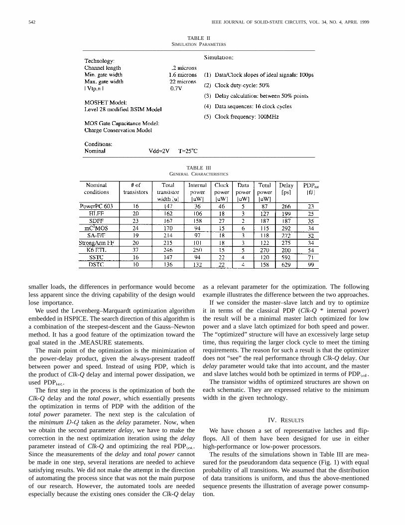
TABLE IISIMULATION PARAMETERS
TABLE IIIGENERAL CHARACTERISTICS
smaller loads, the differences in performance would becomeless apparent since the driving capability of the design wouldlose importance.
We used the Levenberg–Marquardt optimization algorithmembedded in HSPICE. The search direction of this algorithm isa combination of the steepest-descent and the Gauss–Newtonmethod. It has a good feature of the optimization toward thegoal stated in the .MEASURE statements.
The main point of the optimization is the minimization ofthe power-delay product, given the always-present tradeoffbetween power and speed. Instead of using PDP, which isthe product ofClk-Q delay and internal power dissipation, weused PDP .
The first step in the process is the optimization of both theClk-Q delay and thetotal power,which essentially presentsthe optimization in terms of PDP with the addition of thetotal power parameter. The next step is the calculation ofthe minimum - taken as thedelay parameter. Now, whenwe obtain the second parameterdelay, we have to make thecorrection in the next optimization iteration using thedelayparameter instead ofClk-Q and optimizing the real PDP.Since the measurements of thedelay and total powercannotbe made in one step, several iterations are needed to achievesatisfying results. We did not make the attempt in the directionof automating the process since that was not the main purposeof our research. However, the automated tools are neededespecially because the existing ones consider theClk-Q delay
as a relevant parameter for the optimization. The followingexample illustrates the difference between the two approaches.
If we consider the master–slave latch and try to optimizeit in terms of the classical PDP (Clk-Q * internal power)the result will be a minimal master latch optimized for lowpower and a slave latch optimized for both speed and power.The “optimized” structure will have an excessively large setuptime, thus requiring the larger clock cycle to meet the timingrequirements. The reason for such a result is that the optimizerdoes not “see” the real performance throughClk-Q delay. Ourdelayparameter would take that into account, and the masterand slave latches would both be optimized in terms of PDP.
The transistor widths of optimized structures are shown oneach schematic. They are expressed relative to the minimumwidth in the given technology.
IV. RESULTS
We have chosen a set of representative latches and flip-flops. All of them have been designed for use in eitherhigh-performance or low-power processors.
The results of the simulations shown in Table III are mea-sured for the pseudorandom data sequence (Fig. 1) with equalprobability of all transitions. We assumed that the distributionof data transitions is uniform, and thus the above-mentionedsequence presents the illustration of average power consump-tion.
STOJANOVIC AND OKLOBDZIJA: MASTER–SLAVE AND FLIP-FLOP LATCHES 543
Fig. 13. Single-ended structures, overalldelay comparison.
Fig. 14. Differential structures, overalldelay comparison.
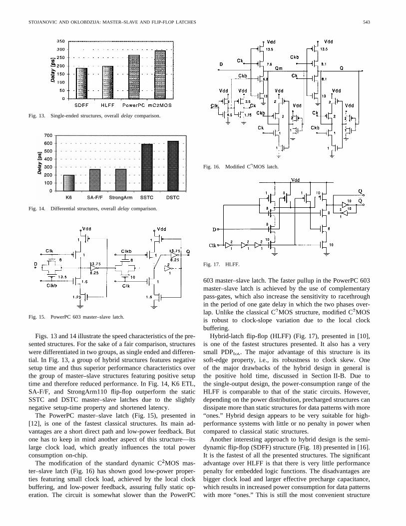
Fig. 15. PowerPC 603 master–slave latch.
Figs. 13 and 14 illustrate the speed characteristics of the pre-sented structures. For the sake of a fair comparison, structureswere differentiated in two groups, as single ended and differen-tial. In Fig. 13, a group of hybrid structures features negativesetup time and thus superior performance characteristics overthe group of master–slave structures featuring positive setuptime and therefore reduced performance. In Fig. 14, K6 ETL,SA-F/F, and StrongArm110 flip-flop outperform the staticSSTC and DSTC master–slave latches due to the slightlynegative setup-time property and shortened latency.
The PowerPC master–slave latch (Fig. 15), presented in[12], is one of the fastest classical structures. Its main ad-vantages are a short direct path and low-power feedback. Butone has to keep in mind another aspect of this structure—itslarge clock load, which greatly influences the total powerconsumption on-chip.
The modification of the standard dynamic CMOS mas-ter–slave latch (Fig. 16) has shown good low-power proper-ties featuring small clock load, achieved by the local clockbuffering, and low-power feedback, assuring fully static op-eration. The circuit is somewhat slower than the PowerPC
Fig. 16. Modified C2MOS latch.
Fig. 17. HLFF.
603 master–slave latch. The faster pullup in the PowerPC 603master–slave latch is achieved by the use of complementarypass-gates, which also increase the sensitivity to racethroughin the period of one gate delay in which the two phases over-lap. Unlike the classical CMOS structure, modified CMOSis robust to clock-slope variation due to the local clockbuffering.
Hybrid-latch flip-flop (HLFF) (Fig. 17), presented in [10],is one of the fastest structures presented. It also has a verysmall PDP . The major advantage of this structure is itssoft-edge property, i.e., its robustness to clock skew. Oneof the major drawbacks of the hybrid design in general isthe positive hold time, discussed in Section II-B. Due tothe single-output design, the power-consumption range of theHLFF is comparable to that of the static circuits. However,depending on the power distribution, precharged structures candissipate more than static structures for data patterns with more“ones.” Hybrid design appears to be very suitable for high-performance systems with little or no penalty in power whencompared to classical static structures.
Another interesting approach to hybrid design is the semi-dynamic flip-flop (SDFF) structure (Fig. 18) presented in [16].It is the fastest of all the presented structures. The significantadvantage over HLFF is that there is very little performancepenalty for embedded logic functions. The disadvantages arebigger clock load and larger effective precharge capacitance,which results in increased power consumption for data patternswith more “ones.” This is still the most convenient structure
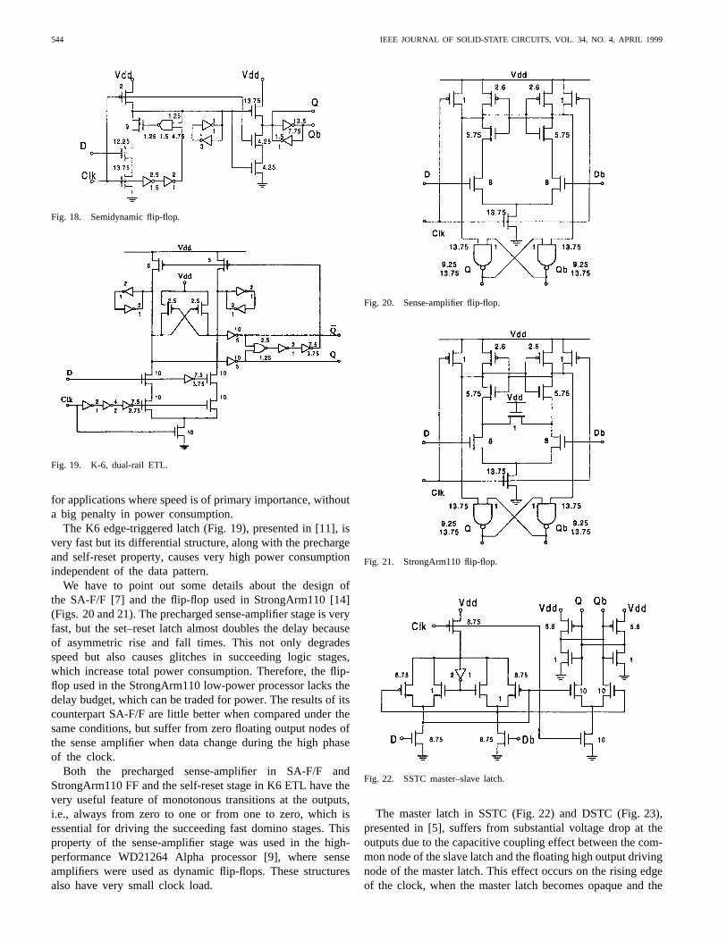
544 IEEE JOURNAL OF SOLID-STATE CIRCUITS, VOL. 34, NO. 4, APRIL 1999
Fig. 18. Semidynamic flip-flop.
Fig. 19. K-6, dual-rail ETL.
for applications where speed is of primary importance, withouta big penalty in power consumption.
The K6 edge-triggered latch (Fig. 19), presented in [11], isvery fast but its differential structure, along with the prechargeand self-reset property, causes very high power consumptionindependent of the data pattern.
We have to point out some details about the design ofthe SA-F/F [7] and the flip-flop used in StrongArm110 [14](Figs. 20 and 21). The precharged sense-amplifier stage is veryfast, but the set–reset latch almost doubles the delay becauseof asymmetric rise and fall times. This not only degradesspeed but also causes glitches in succeeding logic stages,which increase total power consumption. Therefore, the flip-flop used in the StrongArm110 low-power processor lacks thedelay budget, which can be traded for power. The results of itscounterpart SA-F/F are little better when compared under thesame conditions, but suffer from zero floating output nodes ofthe sense amplifier when data change during the high phaseof the clock.
Both the precharged sense-amplifier in SA-F/F andStrongArm110 FF and the self-reset stage in K6 ETL have thevery useful feature of monotonous transitions at the outputs,i.e., always from zero to one or from one to zero, which isessential for driving the succeeding fast domino stages. Thisproperty of the sense-amplifier stage was used in the high-performance WD21264 Alpha processor [9], where senseamplifiers were used as dynamic flip-flops. These structuresalso have very small clock load.
Fig. 20. Sense-amplifier flip-flop.
Fig. 21. StrongArm110 flip-flop.
Fig. 22. SSTC master–slave latch.
The master latch in SSTC (Fig. 22) and DSTC (Fig. 23),presented in [5], suffers from substantial voltage drop at theoutputs due to the capacitive coupling effect between the com-mon node of the slave latch and the floating high output drivingnode of the master latch. This effect occurs on the rising edgeof the clock, when the master latch becomes opaque and the
STOJANOVIC AND OKLOBDZIJA: MASTER–SLAVE AND FLIP-FLOP LATCHES 545
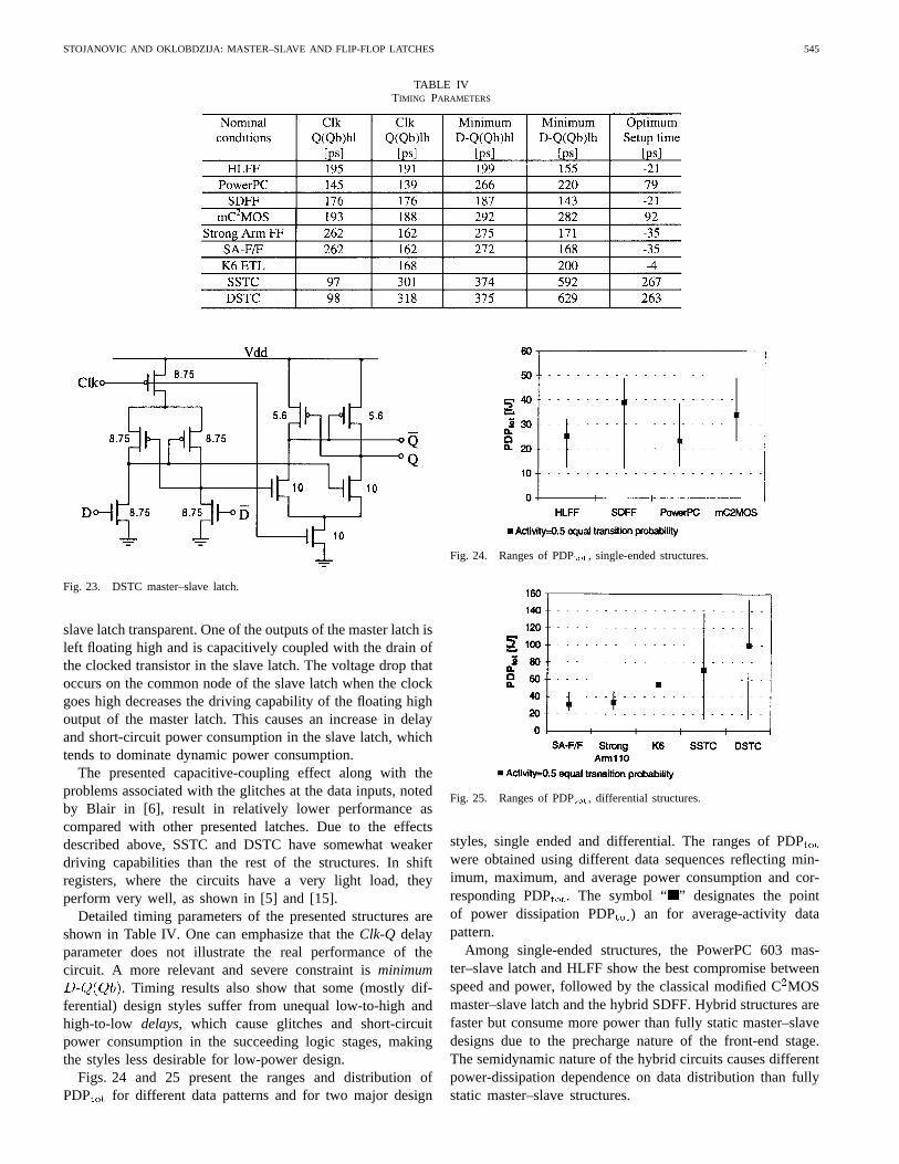
TABLE IVTIMING PARAMETERS
Fig. 23. DSTC master–slave latch.
slave latch transparent. One of the outputs of the master latch isleft floating high and is capacitively coupled with the drain ofthe clocked transistor in the slave latch. The voltage drop thatoccurs on the common node of the slave latch when the clockgoes high decreases the driving capability of the floating highoutput of the master latch. This causes an increase in delayand short-circuit power consumption in the slave latch, whichtends to dominate dynamic power consumption.
The presented capacitive-coupling effect along with theproblems associated with the glitches at the data inputs, notedby Blair in [6], result in relatively lower performance ascompared with other presented latches. Due to the effectsdescribed above, SSTC and DSTC have somewhat weakerdriving capabilities than the rest of the structures. In shiftregisters, where the circuits have a very light load, theyperform very well, as shown in [5] and [15].
Detailed timing parameters of the presented structures areshown in Table IV. One can emphasize that theClk-Q delayparameter does not illustrate the real performance of thecircuit. A more relevant and severe constraint isminimum
- . Timing results also show that some (mostly dif-ferential) design styles suffer from unequal low-to-high andhigh-to-low delays, which cause glitches and short-circuitpower consumption in the succeeding logic stages, makingthe styles less desirable for low-power design.
Figs. 24 and 25 present the ranges and distribution ofPDP for different data patterns and for two major design
Fig. 24. Ranges of PDPtot, single-ended structures.
Fig. 25. Ranges of PDPtot, differential structures.
styles, single ended and differential. The ranges of PDPwere obtained using different data sequences reflecting min-imum, maximum, and average power consumption and cor-responding PDP . The symbol “ ” designates the pointof power dissipation PDP ) an for average-activity datapattern.
Among single-ended structures, the PowerPC 603 mas-ter–slave latch and HLFF show the best compromise betweenspeed and power, followed by the classical modified CMOSmaster–slave latch and the hybrid SDFF. Hybrid structures arefaster but consume more power than fully static master–slavedesigns due to the precharge nature of the front-end stage.The semidynamic nature of the hybrid circuits causes differentpower-dissipation dependence on data distribution than fullystatic master–slave structures.
546 IEEE JOURNAL OF SOLID-STATE CIRCUITS, VOL. 34, NO. 4, APRIL 1999
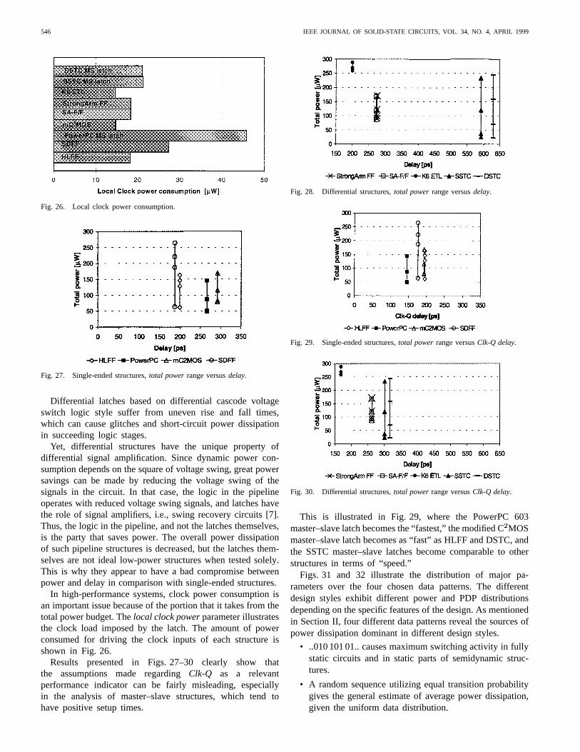
Fig. 26. Local clock power consumption.
Fig. 27. Single-ended structures,total powerrange versusdelay.
Differential latches based on differential cascode voltageswitch logic style suffer from uneven rise and fall times,which can cause glitches and short-circuit power dissipationin succeeding logic stages.
Yet, differential structures have the unique property ofdifferential signal amplification. Since dynamic power con-sumption depends on the square of voltage swing, great powersavings can be made by reducing the voltage swing of thesignals in the circuit. In that case, the logic in the pipelineoperates with reduced voltage swing signals, and latches havethe role of signal amplifiers, i.e., swing recovery circuits [7].Thus, the logic in the pipeline, and not the latches themselves,is the party that saves power. The overall power dissipationof such pipeline structures is decreased, but the latches them-selves are not ideal low-power structures when tested solely.This is why they appear to have a bad compromise betweenpower and delay in comparison with single-ended structures.
In high-performance systems, clock power consumption isan important issue because of the portion that it takes from thetotal power budget. Thelocal clock powerparameter illustratesthe clock load imposed by the latch. The amount of powerconsumed for driving the clock inputs of each structure isshown in Fig. 26.
Results presented in Figs. 27–30 clearly show thatthe assumptions made regardingClk-Q as a relevantperformance indicator can be fairly misleading, especiallyin the analysis of master–slave structures, which tend tohave positive setup times.
Fig. 28. Differential structures,total powerrange versusdelay.
Fig. 29. Single-ended structures,total powerrange versusClk-Q delay.
Fig. 30. Differential structures,total powerrange versusClk-Q delay.
This is illustrated in Fig. 29, where the PowerPC 603master–slave latch becomes the “fastest,” the modified CMOSmaster–slave latch becomes as “fast” as HLFF and DSTC, andthe SSTC master–slave latches become comparable to otherstructures in terms of “speed.”
Figs. 31 and 32 illustrate the distribution of major pa-rameters over the four chosen data patterns. The differentdesign styles exhibit different power and PDP distributionsdepending on the specific features of the design. As mentionedin Section II, four different data patterns reveal the sources ofpower dissipation dominant in different design styles.
• ..010 101 01.. causes maximum switching activity in fullystatic circuits and in static parts of semidynamic struc-tures.
• A random sequence utilizing equal transition probabilitygives the general estimate of average power dissipation,given the uniform data distribution.
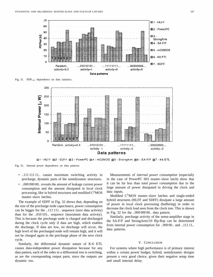
STOJANOVIC AND OKLOBDZIJA: MASTER–SLAVE AND FLIP-FLOP LATCHES 547
Fig. 31. PDPtot dependence on data statistics.
Fig. 32. Internal power dependence on data patterns.
• ..111 111 11.. causes maximum switching activity inprecharge, dynamic parts of the semidynamic structures.
• ..000 000 00.. reveals the amount of leakage current powerconsumption and the amount dissipated in local clockprocessing, like in hybrid structures and modified CMOSmaster–slave latches.
The example of SDFF in Fig. 32 shows that, depending onthe size of the precharge node capacitance, power consumptioncan be bigger for the ..111 111.. sequence (zero data activity)than for the ..010 101.. sequence (maximum data activity).This is because the precharge node is charged and dischargedduring the clock cycle only if data are high, which enablesthe discharge. If data are low, no discharge will occur, thehigh level of the precharged node will remain high, and it willnot be charged again in the precharge phase of the next clockcycle.
Similarly, the differential dynamic nature of K-6 ETLcauses data-independent power dissipation because for anydata pattern, each of the sides in a differential tree is switching,as are the corresponding output parts, since the outputs aredynamic too.
Measurements ofinternal power consumption(especiallyin the case of PowerPC 603 master–slave latch) show thatit can be far less thantotal power consumptiondue to thelarge amount of power dissipated in driving the clock anddata inputs.
Modified C MOS master–slave latches and single-endedhybrid structures (HLFF and SDFF) dissipate a large amountof power in local clock processing (buffering) in order todecrease the clock load seen from the clock tree. This is shownin Fig. 32 for the ..000 000 00.. data pattern.
Similarly, precharge activity of the sense-amplifier stage inthe SA-F/F and StrongArm110 flip-flop can be determinedfrom internal power consumption for ..000 00.. and ..111 11..data patterns.
V. CONCLUSION
For systems where high performance is of primary interestwithin a certain power budget, hybrid, semidynamic designspresent a very good choice, given their negative setup timeand small internal delay.
548 IEEE JOURNAL OF SOLID-STATE CIRCUITS, VOL. 34, NO. 4, APRIL 1999
Fully static MS latches are suitable for low-power appli-cations, where speed is not of primary importance. Amongdifferent single-ended design styles, our work has stated twoas the most suitable for low-power applications: the low-power pass-gate style used in PowerPC 603 and the low-powermodified C MOS style.
Among differential structures, SA-F/F and StrongArm flip-flop offer the best compromise in terms of both power andspeed despite the speed bottleneck in the output stage. Thesestructures offer interface to the low swing logic families andprobably present the mainstream of future design styles.
The problem of consistency in analysis of various latch andflip-flop designs was addressed. A set of consistent analysisapproaches and simulation conditions has been introduced. Westrongly feel that any research on latch and flip-flop designtechniques for high-performance systems should take theseparameters into account. The problems of the transistor widthoptimization methods have also been described. Some hiddenweaknesses and potential dangers in terms of reliability ofprevious timing parameters and optimization methods werebrought to light.
ACKNOWLEDGMENT
The authors gratefully acknowledge suggestions by andnumerous discussions with B. Nikolic, which greatly improvedthis paper and helped them clarify some concepts. They arethankful for the technical support provided by Hitachi AmericaResearch Labs, Dr. Y. Hatano, and Dr. R. Bajwa for theirinsight in simulation and proper evaluation environment aswell as numerous discussions on this subject. They thank S.Oklobdzija for improving the language and presentation ofthis paper.
REFERENCES
[1] S. H. Unger and C. Tan, “Clocking schemes for high-speed digitalsystems,”IEEE Trans. Comput., vol. C-35, pp. 880–895, Oct. 1986.
[2] G. J. Fisher, “An enhanced power meter for SPICE2 circuit simulation,”IEEE Trans. Computer-Aided Design, vol. 7, May 1988.
[3] J. Yuan and C. Svensson, “CMOS circuit speed optimization basedon switch level simulation,” inProc. Int. Symp. Circuits and Systems(ISCAS’88), 1988, pp. 2109–2112.
[4] , “Principle of CMOS circuit power-delay optimization withtransistor sizing,” inProc. Int. Symp. Circuits and Systems (ISCAS’96),1996, vol. 1, pp. 62–69.
[5] , “New single-clock CMOS latches and flipflops with improvedspeed and power savings,”IEEE J. Solid-State Circuits, vol. 32, Jan.1997.
[6] G. M. Blair, “Comments on new single-clock CMOS latches and flip-flops with improved speed and power savings,”IEEE J. Solid-StateCircuits, vol. 32, pp. 1610–1611, Oct. 1997.
[7] M. Matsui, H. Hara, Y. Uetani, K. Lee-Sup, T. Nagamatsu, Y. Watanabe,A. Chiba, K. Matsuda, and T. Sakurai, “A 200 MHz 13 mm2 2-DDCT macrocell using sense-amplifier pipeline flip-flop scheme,”IEEEJ. Solid-State Circuits, vol. 29, pp. 1482–1491, Dec. 1994.
[8] J. Montanaro, R. T. Witek, K. Anne, A. J. Black, E. M. Cooper, D.W. Dobberpuhl, P. M. Donohue, J. Eno, W. Hoeppner, D. Kruckemyer,T. H. Lee, P. C. M. Lin, L. Madden, D. Murray, M. H. Pearce, S.Santhanam, K. J. Snyder, R. Stephany, and S. C. Thierauf, “A 160-MHz, 32-b, 0.5-W CMOS RISC microprocessor,”IEEE J. Solid-StateCircuits, vol. 31, pp. 1703–1714, Nov. 1996.
[9] B. A. Gieseke, R. L. Allmon, D. W. Bailey, B. J. Benschneider, S. M.Britton, J. D. Clouser, H. R. Fair, J. A. Farrell, M. K. Gowan, C. L.Houghton, J. B. Keller, T. H. Lee, D. L. Leibholz, S. C. Lowell, M.D. Matson, R. J. Matthew, V. Peng, M. D. Quinn, D. A. Priore, M. J.Smith, and K. E. Wilcox, “A 600 MHz superscalar RISC microprocessor
with out-of-order execution,” inISSCC Dig. Tech. Papers, Feb. 1997,pp. 176–177, 451.
[10] H. Partovi, R. Burd, U. Salim, F. Weber, L. DiGregorio, and D. Draper,“Flow-through latch and edge-triggered flip-flop hybrid elements,” inISSCC Dig. Tech. Papers, Feb. 1996, pp. 138–139.
[11] D. Draper, M. Crowley, J. Holst, G. Favor, A. Schoy, J. Trull, A. Ben-Meir, R. Khanna, D. Wendell, R. Krishna, J. Nolan, D. Mallick, H.Partovi, M. Roberts, M. Johnson, and T. Lee, “Circuit techniques in a266-MHz MMX-enabled processor,”IEEE J. Solid-State Circuits, vol.32, pp. 1650–1664, Nov. 1997.
[12] G. Gerosa, S. Gary, C. Dietz, P. Dac, K. Hoover, J. Alvarez, H. Sanchez,P. Ippolito, N. Tai, S. Litch, J. Eno, J. Golab, N. Vanderschaaf, and J.Kahle, “A 2.2 W, 80 MHz superscalar RISC microprocessor,”IEEE J.Solid-State Circuits, vol. 29, pp. 1440–1452, Dec. 1994.
[13] M. Shoji, Theory of CMOS Digital Circuits and Circuit Fail-uresPrinceton, NJ: Princeton Univ. Press, 1992.
[14] U. Ko, A. Hill, and P. T. Balsara, “Design techniques for high-performance, energy-efficient control logic,” inISLPED Dig. Tech.Papers, Aug. 1996.
[15] C. Svensson and J. Yuan, “Latches and flip-flops for low powersystems,” in Low Power CMOS Design,A. Chandrakasan and R.Brodersen, Eds. Piscataway, NJ: IEEE Press, 1998, pp. 233–238.
[16] F. Klass, “Semi-dynamic and dynamic flip-flops with embedded logic,”in 1998 Symp. VLSI Circuits Dig. Tech. Papers, Honolulu, HI, June11–13, 1998, pp. 108–109.
Vladimir Stojanovic was born in Kragujevac, Ser-bia, Yugoslavia, on August 2, 1974. He receivedthe Dipl.Ing. degree in electrical engineering fromthe University of Belgrade, Yugoslavia, in 1998. Hecurrently is pursuing the M.Sc. degree in the Depart-ment of Electrical Engineering, Stanford University,Stanford, CA.
In 1997–1998, he was a Visiting Scholar in theAdvanced Computer Systems Engineering Labo-ratory, University of California, Davis, where heconducted research in the area of latches and flip-
flops for low-power and high-performance VLSI systems. His current researchinterests include analog and digital IC’s and architectures for low-power,portable systems.
Vojin G. Oklobdzija (S’78–M’82–SM’88–F’95)received the M.Sc. and Ph.D. degrees in computerscience from the University of California, LosAngeles (UCLA), in 1982 and 1978, respectively.He received the Dipl.Ing. (M.Sc.E.E.) degreein electronics and telecommunication from theElectrical Engineering Department, University ofBelgrade, Yugoslavia, in 1971.
He was on the Faculty at the University ofBelgrade until 1976. Currently he is Presidentand CEO of Integration Corp., Berkeley, CA. He
spent eight years as a Research Staff Member with the IBM T. J. WatsonResearch Center, Yorktown Heights, NY, where he made contributions tothe development of RISC and superscalar RISC architecture and receiveda patent on the IBMRS/6000-PowerPC. From 1988 to 1990 he was withthe University of California, Berkeley, as Visiting Faculty from IBM. Hisindustrial experience includes positions with the Microelectronics Center ofXerox Corp. and consulting positions with Sun Microsystems Laboratories,AT&T Bell Laboratories, Siemens, Hitachi Laboratories, Sony Corp., andvarious others. His interests are in computer design and architecture, VLSI,fast circuits, and efficient implementations of algorithms and computation. Hehas received four U.S. and four European patents in the area of circuits andcomputer design and has six patents pending. He is the author or coauthorof more than 100 papers in the areas of circuits and technology, computerarithmetic, and computer architecture and of a book on high-performancesystem design.
Dr. Oklobdzija is a member of the American Association of UniversityProfessors and the IEICE of Japan. He is a member of the editorial board ofthe IEEE TRANSACTIONS ONVERY LARGE SCALE INTEGRATED (VLSI) SYSTEMS
and the Journal of VLSI Signal Processing. He is a Program CommitteeMember of the International Solid-State Circuits Conference and was aGeneral Cochairman of the 1997 Symposium on Computer Arithmetic. Hewas a Fulbright Scholar at UCLA in 1976 and a Fulbright Professor in Peruin 1991.