Compact modeling of junctionless nanowire MOSFETs
21
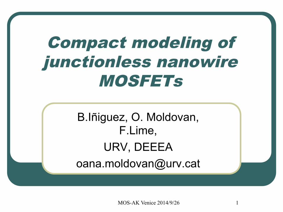
MOS-AK Venice 2014/9/26 1 Compact modeling of junctionless nanowire MOSFETs B.Iñiguez, O. Moldovan, F.Lime, URV, DEEEA [email protected]
Transcript of Compact modeling of junctionless nanowire MOSFETs
MOS-AK Venice 2014/9/26 1
Compact modeling of junctionless nanowire
MOSFETs
B.Iñiguez, O. Moldovan, F.Lime,
URV, DEEEA [email protected]

MOS-AK Venice 2014/9/26
2
Outline l Introduction l Drain current and charge models in depletion l Drain current and charge models in
accumulation l Unified drain current model l Capacitance model l Results l Conclusion
MOS-AK Venice 2014/9/26
3
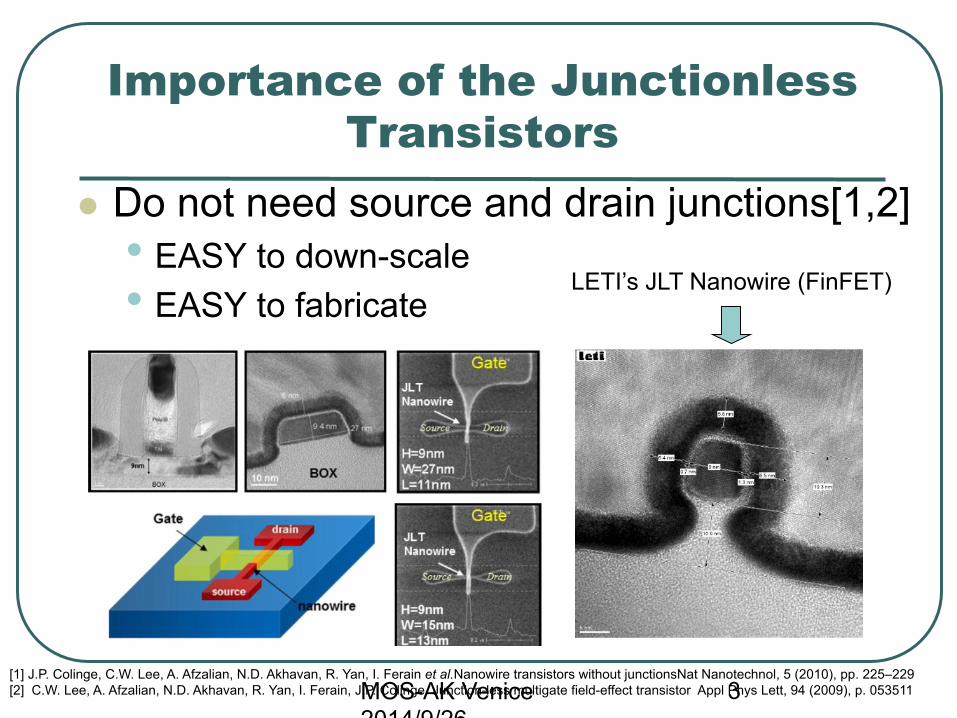
Importance of the Junctionless Transistors
l Do not need source and drain junctions[1,2] • EASY to down-scale • EASY to fabricate
LETI’s JLT Nanowire (FinFET)
[1] J.P. Colinge, C.W. Lee, A. Afzalian, N.D. Akhavan, R. Yan, I. Ferain et al.Nanowire transistors without junctionsNat Nanotechnol, 5 (2010), pp. 225–229 [2] C.W. Lee, A. Afzalian, N.D. Akhavan, R. Yan, I. Ferain, J.P. Colinge Junction-less multigate field-effect transistor Appl Phys Lett, 94 (2009), p. 053511
MOS-AK Venice 2014/9/26
4 4
Junctionless Transistors
l Implementation in integrated circuits is NECESSARY
• NEED of compact models adequate for circuit simulators • better computation speed
l Circuit design requires a complete small-signal model • analytical expressions of total capacitances
MOS-AK Venice 2014/9/26
5
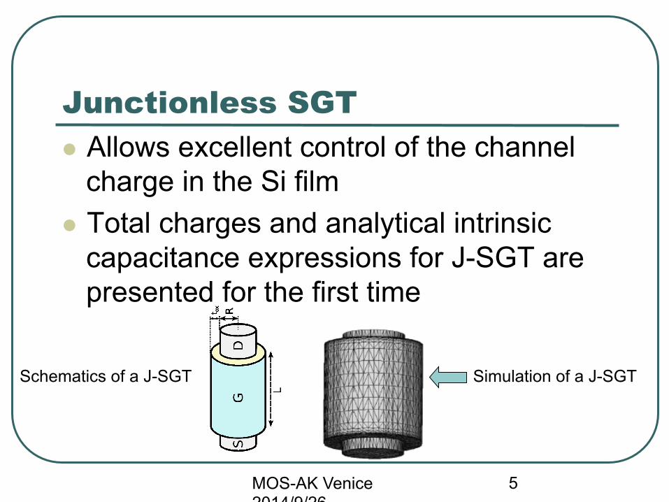
Junctionless SGT l Allows excellent control of the channel
charge in the Si film l Total charges and analytical intrinsic
capacitance expressions for J-SGT are presented for the first time
Simulation of a J-SGT Schematics of a J-SGT

MOS-AK Venice 2014/9/26
6
Electrostatic analysis
Parabolic potential approximation
This leads to:
MOS-AK Venice 2014/9/26
7
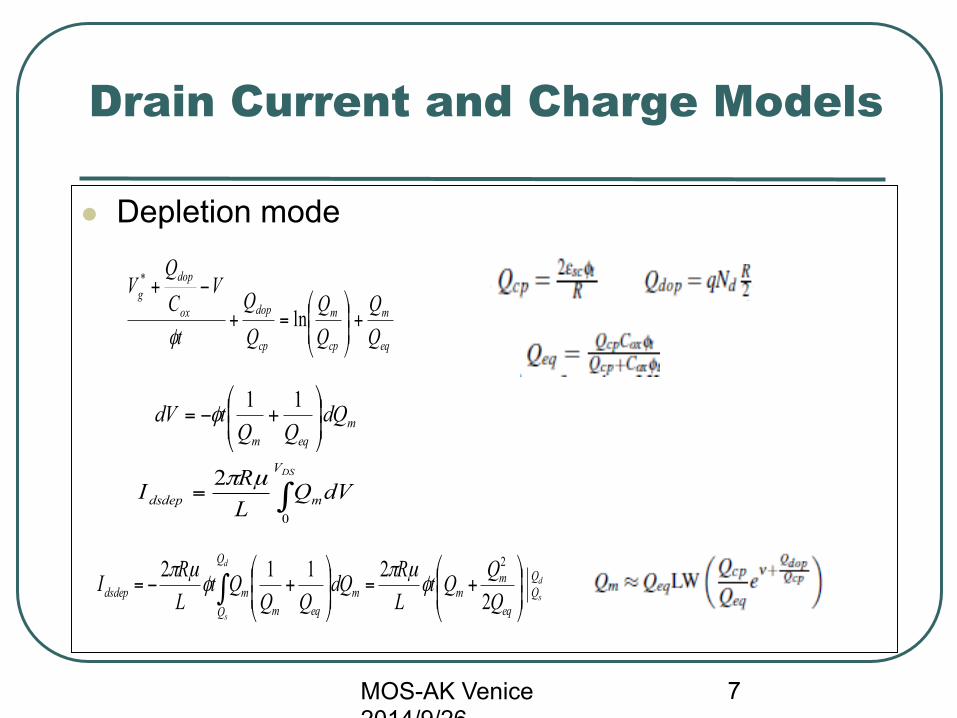
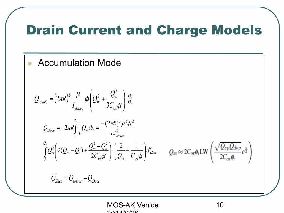
Drain Current and Charge Models
l Depletion mode
eq
m
cp
m
cp
dopox
dopg
t
VCQ
V+⎟⎟⎠
⎞⎜⎜⎝
⎛=+
−+
ln
*
φ
meqm
dQQQ
tdV ⎟⎟⎠
⎞⎜⎜⎝
⎛+−=11
φ
dVQLRI
DSV
mdsdep ∫=0
2 µπ
d
s
d
s
eq
mmm
Q
Q eqmmdsdep Q
QQtLRdQ
QQQt
LRI ⎟
⎟⎠
⎞⎜⎜⎝
⎛+=⎟
⎟⎠
⎞⎜⎜⎝
⎛+−= ∫ 2
2112 2
φµπ
φµπ

MOS-AK Venice 2014/9/26
8
Drain Current and Charge Models
l Depletion mode
( ) dVQI
RdxQRQDSV
mdsdep
L
mtotdep ∫∫ −=−=0
22
0
22 µππ
( ) d
s
eq
mm
dsdeptotdep Q
QQt
IRQ ⎟
⎟⎠
⎞⎜⎜⎝
⎛+=32
232
2 φµ
π
meqmeq
smsm
Q
Qm
dsdepm
L
Ddep dQQQQ
QQQQQ
LItRdxQ
LxRQ
d
s
⎟⎟⎠
⎞⎜⎜⎝
⎛+⋅⎟
⎟⎠
⎞⎜⎜⎝
⎛ −+−
−=−= ∫∫
112
)2(222
22
223
0
φµππ
DdeptotdepSdep QQQ −=

MOS-AK Venice 2014/9/26
9
Drain Current and Charge Models
l Accumulation Mode
tCQ
QQQ
t
VCQ
V
ox
m
cpdop
mox
dopg
φφ+⎟⎟⎠
⎞⎜⎜⎝
⎛=
−+ 2*
ln
moxm
dQtCQ
tdV ⎟⎟⎠
⎞⎜⎜⎝
⎛+−=
φφ
12
d
s
ox
mmdsacc tC
QQt
LRI ⎟⎟
⎠
⎞⎜⎜⎝
⎛+−=
φφ
µπ2
22 2
MOS-AK Venice 2014/9/26
10
Drain Current and Charge Models
l Accumulation Mode
( ) d
s
ox
mm
dsacctotacc tC
QQtI
RQ ⎟⎟⎠
⎞⎜⎜⎝
⎛+=
φφ
µπ
32
322
moxmox
smsm
Q
Qm
dsaccm
L
Dacc
dQtCQtC
QQQQQ
LItRdxQ
LxRQ
d
s
⎟⎟⎠
⎞⎜⎜⎝
⎛+⋅⎟⎟
⎠
⎞⎜⎜⎝
⎛ −+−
−=−=
∫
∫
φφ
φµππ
122
)(2
)2(2
222
2
223
0
DacctotaccSacc QQQ −=

MOS-AK Venice 2014/9/26
11
Unified Drain Current Model
l An approximate solution of:

MOS-AK Venice 2014/9/26
12
Unified Drain Current Model
With A=1,425

MOS-AK Venice 2014/9/26
13
Intrinsic Capacitance Model
l The complete capacitance model = sum of
capacitances in depletion and accumulation modes sewed together by a tanh function
jiVQ
VQ
C
jiVQ
VQ
C
j
j
j
accidep
j
accidepaccijdep
j
j
j
accidep
j
accidepaccijdep
=∂
∂
∂
∂=
∂
∂=
≠∂
∂
∂
∂−=
∂
∂−=
.
.
///
///
( )[ ] ( )[ ]⎟⎟⎠
⎞⎜⎜⎝
⎛ +−+⎟⎟⎠
⎞⎜⎜⎝
⎛ +−=
221tanh1
221tanh1 ** qqV
CqqV
CC gijacc
gijdepij
MOS-AK Venice 2014/9/26
14
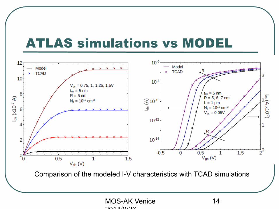
ATLAS simulations vs MODEL
Comparison of the modeled I-V characteristics with TCAD simulations
MOS-AK Venice 2014/9/26
15
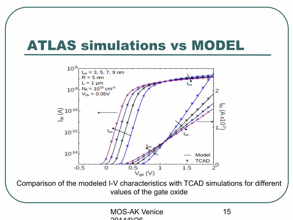
ATLAS simulations vs MODEL
Comparison of the modeled I-V characteristics with TCAD simulations for different values of the gate oxide

MOS-AK Venice 2014/9/26
16
ATLAS simulations vs MODEL
-0.5 0 0.5 1 1.5 2 2.5 3-2
0
2
4
6
8
10
12
14
16 x 10-17
VGS [V]
Capa
citan
ce [F
]
CDS
CGS
CGD
CDD
Ndop
=1x1019cm-3
VDS
=0.05VR=5nmtox
=5nmL=1um
----------- Model results Symbol- Atlas simulations
-0.5 0 0.5 1 1.5 2 2.5 3-5
0
5
10
15
20 x 10-17
VGS [V]
Capa
citan
ce [F
]
CGS
CGD
CDS
CDD
Ndop=1x1019cm-3
VDS=1VR=5nmtox=5nmL=1um
----------- Model resultsSymbol- Atlas simulations
By computing four out of the nine possible intrinsic capacitances we can, afterwards, calculate the other five

MOS-AK Venice 2014/9/26
17
ATLAS simulations vs MODEL
0 0.2 0.4 0.6 0.8 1
0.6
0.8
1
1.2
1.4
1.6
1.8
2 x 10-16
VDS [V]
Capa
citan
ce [F
]
CGD
CDD
CDS
CGS
----------- Model resultsSymbol- Atlas simulations
Ndop
=1x1019cm-3
VGS
=2V R=5nm t
ox=5nm
L= 1um
-0.5 0 0.5 1 1.5 2 2.5 3-2
0
2
4
6
8
10
12
14
16x 10-17
VGS
[V]
Capac
itance
[F] C
DD
CDS
CGS
=CGD
Ndop
=1x1019cm-3
VDS
=0VR=5nmtox
=5nmL=1um
----------- Model results Symbol- Atlas simulations
0/0 Instability d
dgg V
QRLC∂
∂−= π2
DSSDDDSSDGSGGDGSgg CCCCCCCCC 663·32222 −=−=======

MOS-AK Venice 2014/9/26
18
CGG =CGS+CGD for R=5nm and R=10nm
l R=5nm–no ‘distorsions’ l similar capacitance curve as for inversion transistors l R=10nm – see ‘distorsions’
-2 -1 0 1 2 30
1
2
3
4
5
6 x 10-16
VGS [V]
CG
G [
F]
Ndop=1x1019cm-3
VDS=1Vtox=5nmL=1um
- Model results for R=5nm---Model results for R=10nm Symbol- Atlas simulations
Vth
VFB VFB
Vth

MOS-AK Venice 2014/9/26
19
-2 -1 0 1 2 30
0.5
1
1.5
2
2.5
3
3.5x 10⁻¹⁶
VGS [V]
C GG [F
]
--- Model results Ndop=2x1019cm-3
-Model results Ndop=4x1019cm-3
Symbol- Atlas simulations
VDS=1VR=5nmtox=5nmL=1um
CGG for different Ndop
As Vth becomes more negative, the transition part becomes
more visible
Which is the optimum Si thickness versus doping combination???

MOS-AK Venice 2014/9/26
20
Advantages of our model
l Explicit and anlaytic l Very simple and easy to implement l Reproduces well the two different conduction
modes: accumulation & depletion l Good agreement with 3D numerical
simulations l Some limitations, but not regarding a real
device

MOS-AK Venice 2014/9/26
21
Thank you for your attention!