Compact Isolated High Frequency DC/DC Converters Using ... · vii ACKNOWLEDGMENTS With deep...
101
Compact Isolated High Frequency DC/DC Converters Using Self-Driven Synchronous Rectification Douglas R. Sterk Thesis submitted to the Faculty of the Virginia Polytechnic Institute and State University in partial fulfillment of the requirements for the degree of Masters of Science in Electrical Engineering Dr. Fred C. Lee, Chairman Dr. Dushan Boroyevich Dr. William Baumann December 17, 2003 Blacksburg, Virginia Tech Keywords: self-driven, integrated transformer, integrated magnetics, distributed power systems Copyright 2003, Douglas R. Sterk
Transcript of Compact Isolated High Frequency DC/DC Converters Using ... · vii ACKNOWLEDGMENTS With deep...

Compact Isolated High Frequency DC/DC Converters Using Self-Driven Synchronous Rectification
Douglas R. Sterk
Thesis submitted to the Faculty of the Virginia Polytechnic Institute and State University
in partial fulfillment of the requirements for the degree of
Masters of Science
in
Electrical Engineering
Dr. Fred C. Lee, Chairman
Dr. Dushan Boroyevich
Dr. William Baumann
December 17, 2003 Blacksburg, Virginia Tech
Keywords: self-driven, integrated transformer, integrated magnetics, distributed power
systems
Copyright 2003, Douglas R. Sterk

ii

iii
Compact Isolated High Frequency DC/DC Converters
Using Self-Driven Synchronous Rectification
Douglas R. Sterk
(ABSTRACT)
In the early 1990’s, with the boom of the Internet and the advancements in
telecommunications, the demand for high-speed communications systems has reached
every corner of the world in forms such as, phone exchanges, the internet servers, routers,
and all other types of telecommunication systems. These communication systems
demand more data computing, storage, and retrieval capabilities at higher speeds, these
demands place a great strain on the power system. To lessen this strain, the existing
power architecture must be optimized.
With the arrival of the age of high speed and power hungry microprocessors, the
point of load converter has become a necessity. The power delivery architecture has
changed from a centralized distribution box delivering an entire system’s power to a
distributed architecture, in which a common DC bus voltage is distributed and further
converted down at the point of load. Two common distributed bus voltages are 12 V for
desktop computers and 48 V for telecommunications server applications. As industry
strives to design more functionality into each circuit or motherboard, the area available
for the point of load converter is continually decreasing. To meet industries demands of
more power in smaller sizes power supply designers must increase the converter’s
switching frequencies. Unfortunately, as the converter switching frequency increases the
efficiency is compromised. In particular, the switching, gate drive and body diode related
losses proportionally increase with the switching frequency.
This thesis introduces a loss saving self-driven method to drive the secondary side
synchronous rectifiers. The loss saving self-driven method introduces two additional
transformers that increase the overall footprint of the converter. Also, this thesis
proposes a new magnetic integration method to eliminate the need for the two additional

iv
gate driver magnetic cores by allowing three discrete power signals to pass through one
single magnetic structure. The magnetic integration reduces the overall converter
footprint.

v
To my wife
Elizabeth Jewel

vi
(this page intentionally left blank)

vii
ACKNOWLEDGMENTS
With deep appreciation, I would like to thank my advisor, Dr. Fred C. Lee for his
guidance, leadership and, and most of all, for inspiring me to be a better engineer. His
profound ability to illustrate the logic in research and to drive all of his students to work
to their full potential is remarkable. I would also like to thank Dr. Lee for his wonderful
attitude and for always having a smile on his face.
I am grateful to my committee members, Dr. Dushan Boroyevich and Dr. William
Baumann for their commitment to serving on my committee. Dr. Boroyevich
undergraduate classes in power electronics sparked my initial interest in power
electronics. Dr. Baumann’s undergraduate controls classes gave me a better
understanding of controls and the operation of electronic circuitry.
I would also like to thank Dr. Dan Chen, for his enthusiasm and methods in
teaching the undergraduate Electronics II classes. If it were not for Dr. Chen teaching
this class I would most likely be a businessman. His approach to teaching reinforced my
want to be an electrical engineer.
My family and I would like to Mrs. Marion Bradley Via, Edward Via and the Via
Family as well as John Rocovich for endowing the Harry Lynde Bradley Fellowship
support to me.
It has been a great pleasure to work in the Center for Power Electronics Systems
(CPES). I would like to thank extraordinary staff, Ms. Linda Gallagher, Ms. Teresa
Shaw, Ms. Trish Rose, Ms. Ann Craig, Ms. Marianne Hawthorne, Ms. Elizabeth Tranter,
Mr. Steve Chen, Mr. Robert Martin, Mr. Jamie Evans, Mr. Dan Huff, Mr. Gary Kerr, Mr.
Ben Pfountz, Mr. Matt Pfountz, and Mr. David Fuller, as well as Ms. Cindy Hopkins in
the Graduate Advising office. Special thanks are due to my fellow students and visiting
scholars for their help and friendship: Mr. Francisco Canales, Mr. Dimos Katsis, Mr.
Jerry Francis, Mr. Qun Zhao, Mr. Wei Dong, Mr. Bo Yang, Mr. Bing Lu, Mr. Roger
Chen, Ms. Jinghong Guo, Mr. Ali Hajjiah, Mr. John Reichl, Mr. Josh Hawley, and Mr.
Yonghan Kang,

viii
It has been my pleasure and good luck to work with the talented, and dedicated,
and team oriented colleagues in the VRM group. I would like to thank Dr. Ming Xu for
being an exceptional team leader not only driving myself but the entire VRM group to
excel in research and everyday life. I would also like to thank all the members of my
research team: Mr. Gary Yao, Mr. Yuancheng Ren, Mr. Jinghai Zhou, Mr. Arthur Ball,
Mr. Jia Wei, Mr. Yu Meng, Mr. Yang Qui, Mr. Kisun Lee, Mr. Mau Ye, Mr. Ju Lu Sun,
Ms. Juanjuan Su, Ms. Ma Li, Mr. Liyu Yang, Mr. Zhenjian Liang and Ms. Yan Jiang.
Finally, special thanks goes to my family and life long friends for the support you
provided on a constant basis during my educational career. Your love, encouragement,
and inspiration have driven me to this point in my life and help to shape my future. To
my dad, Roger Sterk Sr., my mother Dianne Root, my brothers Roger Sterk Jr., Michael
Sterk, Jeremy Bendler, my wife Elizabeth Jewel and her family Mike, Maurene and Erin
Jewel and to Michael Mayberry, Kelly Stephenson and Jonathan and Paige Holleran. I
could not have done this without you guys.
This work was supported by the VRM consortium (Delta Electronic, Hipro
Electronics, Renesas, Intel, Intersil, National Semiconductor, Power-One, TDK, Texas
Instruments and Infineon) and the ERC program of the National Science Foundation
under award number EEC-9731677.

ix
TABLE OF CONTENTS
Chapter 1 Introduction ...................................................................................................... 1
1.1 Background and Objectives .................................................................................... 1
1.2 Thesis Outline ......................................................................................................... 5
Chapter 2 Development of a Zero-Voltage-Switched Complimentary Controlled Full Bridge with Self-Driven Synchronous Rectification .......................................................... 7
2.1 Secondary Side Rectifier Topologies........................................................................ 7
2.2 External Gate Drivers vs. Self-Driven Gate Drivers .............................................. 10
2.3 Zero-Voltage-Switched Phase-Shifted Full Bridge ................................................ 17
2.4 Complementary Controlled Full Bridge with a Current-Doubler........................... 23
2.5 Steady-State Operation of the Proposed Self-Driven Scheme................................ 28
2.6 Transient Operation of the Self-Driven Scheme..................................................... 36
2.7 Summary................................................................................................................. 46
Chapter 3 Performance Improvements of Integrating Multiple Transformers ............... 49
3.1 Motivation............................................................................................................... 49
3.2 Derivation of the Integrated Transformer............................................................... 52
3.2 Analysis of the Integrated Transformer Structure .................................................. 59
3.3 Loss Calculations in the Integrated Transformer.................................................... 64
3.4 Experimental Results for the Self-Driven Complementary Controlled Full Bridge with Integrated Transformer ......................................................................................... 69
3.5 Summary................................................................................................................. 74
Chapter 4 Conclusions and Future Work........................................................................ 75
4.1 Summary................................................................................................................. 75
4.2 Future Work............................................................................................................ 76
REFERENCES ............................................................................................................. 81
Vita.................................................................................................................................... 87

x
(this page intentionally left blank)

xi
LIST OF ILLUSTRATIONS
Fig. 1.1. Single magnetic push-pull forward converter with a built-in input filter and coupled-inductor current doubler……………………………………………...2
Fig. 1.2. Efficiency curve for the single magnetic push-pull forward converter with a built-in input filter and coupled-inductor current doubler…………….….…3
Fig. 1.3. Loss breakdown for the single magnetic push-pull forward converter with a built-in input filter and coupled-inductor current doubler operating at 1.2V / 70 A, with a switching frequency of 100 kHz……………………………....3
Fig. 1.4. Loss breakdown comparison for the single magnetic push-pull forward converter with a built-in input filter and coupled-inductor current doubler operating at 1.2V / 70 A, with switching frequencies of 100 kHz and 500 kHz…...4
Fig. 2.1. (a) Full-wave rectifier, (b) Forward rectifier, (c) Center-tap rectifier, and (d) Current-doubler rectifier…………………………..…………………….. 8
Fig. 2.2. Secondary side transformer waveforms (a) asymmetrical, (b) symmetrical….... 9
Fig. 2.3. Loss breakdown of a half-bridge converter with a current doubler secondary operated at 100 kHz and 1 MHz…………………………………………..…11
Fig. 2.4. (a) Conventional Gate Driver (b) Operating waveforms……………………….12
Fig. 2.5. (a) Resonant MOSFET gate driver (b) Operating waveforms ….…………... .13
Fig. 2.6. (a) Half-bridge with self-driven current-doubler secondary, (b) Secondary side transformer waveform……………………………………………………………14
Fig. 2.7. Jose A. Cobos’ self-driven circuit utilizing an auxiliary winding and two diodes…………………………………………………………………………….15
Fig. 2.8. The auxiliary winding voltage and the VGS waveforms for one synchronous rectifier shown in Fig. 2.7………………………………………………………..16
Fig. 2.9. (a) Phase shifted full bridge topology, (b) Ideal phase-shift operation……….. 18
Fig. 2.10. Circuit timing operation of the phase-shift full bridge………………………...19
Fig. 2.11. (a) Full ZVS operation, (b) ZVS met, extra circulating energy (c) Partial ZVS, not enough energy to meet ZVS requirement…………………………... .22
Fig. 2.12. Comparison of the phase-shift and the complementary control operations….....23
Fig. 2.13. The complementary control full-bridge with a current-doubler secondary side…………………………………………………………………….………...24
Fig. 2.14. Operation of the complementary-controlled full bridge with the current- doubler secondary side…………………………………………………….…….25
Fig. 2.15. Complementary-controlled full bridge with self-driven synchronous rectifiers………………………………………………………………………....27

xii
Fig. 2.16. Path of the gate drive current during complete non-ZVS (a) turn on and
(b) turn off of the synchronous rectifiers………………………………………...28
Fig. 2.17. Operating waveforms for the self-driven circuit under a non-ZVS operating condition………………………………………………………………29
Fig. 2.18. Key operating waveforms for the self-driven complementary-controlled full bridge detailing one switching cycle of the self driven circuit……………...30
Fig. 2.19. Topological stage for the self-driven circuit at time t0………………………..31
Fig. 2.20. Topological stage for the self-driven circuit at time t1………………………..32
Fig. 2.21. Topological stage for the self-driven circuit at time t2………………………..33
Fig. 2.22. Topological stage for the self-driven circuit at time t3………………………..34
Fig. 2.23. Topological stage for the self-driven circuit at time t4………………………..34
Fig. 2.24. Topological stage for the self-driven circuit at time t5………………………..35
Fig. 2.25. Self-driven gate drive circuit with damping resistor………………………….36
Fig. 2.26. Equivalent circuit diagram for the self-driven circuit………………………...37
Fig. 2.27. Turn on loss comparison of the self-driven circuit vs. a conventional external voltage driver, both operating at 1MHz for 5 HAT2165 in parallel...….38
Fig. 2.28. Turn-off loss comparison of the self-driven circuit vs. a conventional external voltage driver, both operating at 1Mhz for 5 HAT2165 in parallel..…...38
Fig. 2.29. Test waveforms of a self-driven complementary-controlled full bridge operating at 650 kHz. (top waveform) VGS of a synchronous rectifier, (bottom waveform) voltage across a 0.5 Ω gate drive resistor…………….……39
Fig. 2.30. Self-driven circuit with the additional tiny MOSFET………………………...40
Fig. 2.31. Test waveforms of a self-driven complementary-controlled full bridge operating at 650 kHz. (top waveform) VGS of a synchronous rectifier, (middle waveform) VGS of the tiny MOSFET, (bottom waveform) voltage across a 0.5 Ω gate drive resistor………….……………………………………41
Fig. 2.32. Self-driven gate drive circuit with a delay in the tiny MOSFET gate drive path………………………………………………………………………..42
Fig. 2.33. Operational waveforms of the self-driven circuit shown in Fig. 2.32………...43
Fig. 2.34. Comparison between the body diode conduction times (a) Phase-shift full bridge, (b) Self-Driven complementary-controlled full bridge. Highlighted are the body diode conduction times……………………………….44
Fig. 2.35. Body diode conduction loss comparison…………………………………….45
Fig. 2.36. Efficiency comparison of the self-driven circuit with a fast tiny MOSFET and a delayed tiny MOSFET operating 650 kHz with an output of 1.2V and an input of 48V……………………………………………………..45

xiii
Fig. 3.1. Mechanical diagram of a PowerQor Tera PQ60012QTA40 quarter-brick
from Synqor……………………………………………………….……………....50
Fig. 3.2. A topological arrangement for the three gate drive transformers and two output inductors…………………………………………………………………...51
Fig. 3.3. Complementary-controlled full bridge with self-driven synchronous rectifiers…………………………………………………………………………..53
Fig. 3.4. The operational waveforms of the power transformer and point A and point B………………………………………………………………………….....53
Fig. 3.5. From time t0 to t1 (a) First power delivery topological state (b) Resulting flux in the three transformers. The arrows state the direction of the AC flux in the cores………………………………………………………………………..54
Fig. 3.6. From time t1 to t2 (a) Second freewheeling topological state (b) Resulting flux in the three transformers. The arrows state the direction of the AC flux in the cores………………………………………………………………………..55
Fig. 3.7. From time t2 to t3 (a) Second power delivery topological state (b) Resulting flux in the three transformers. The arrows state the direction of the AC flux in the cores………………………………………………………………………..56
Fig. 3.8. From time t3 to t4 (a) Second freewheeling topological state (b) Resulting flux in the three transformers. The arrows state the direction of the AC flux in the cores……………………………………………………………………......56
Fig. 3.9. Integrated transformer windings………………………………………………..58
Fig. 3.10. Integrated transformer winding structure……………………………………...58
Fig. 3.11. Basic inductor…………………………………………………………………59
Fig. 3.12. Basic Transformer (a) circuit implementation, (b) physical implementation…………………………………………………………………...60
Fig. 3.13. Multiple primary winding structure……………………………………….….60
Fig. 3.14. Reluctance models………………………………………………………….…61
Fig. 3.15. Schematic of the self-driven complementary-controlled full bridge with the integrated transformer…………………………………….…….………62
Fig. 3.16. Winding structure for the self-driven complementary-controlled full bridge with the integrated transformer…………………………………………………..62
Fig. 3.17. Primary side transformer waveforms for the self-driven complementary controlled full-bridge with the integrated transformer…………………………...63
Fig. 3.18. (a) Diagram of a simple transformer (b) sketch of the cross-sectional area of an EE/EI core, (c) flux diagram of integrated transformer showing primary side windings…………………………………………………………………….65
Fig. 3.19. Flux distribution areas………………………………………………………...67

xiv
Fig. 3.20. Maxwell 2D simulation of the integrated transformer………………………....68
Fig. 3.21. Self-driven complementary-controlled full bridge, (left) discrete transformers and (right) integrated transformer…………………………………..70
Fig. 3.22. Customized core for the integrated transformer design in (mm)..……………...71
Fig. 3.23. Operational waveforms. (a) The discrete transformer case, (b) Integrated transformer case. Top waveform is the primary side main transformer current, middle is the secondary side gate drive voltage, and bottom is Point A (B) corresponding to the gate drive waveform……………………………………….71
Fig. 3.24. Efficiency curve comparison……………………………………………….....72
Fig. 3.25. Loss breakdown for the 9-Layer 2-oz. copper integrated transformer case…...72
Fig. 3.26. Improved layout of the self-driven complementary-controlled full-bridge with the integrated transformer…………………………………………………...73
Fig. 3.27. Efficiency curve for the improved layout of the self-driven complementary- controlled full bridge with the integrated transformer…………………………....74
Fig. 4.1. Integrated current doubler rectifier proposed by Prof. W. Chen…………….….76
Fig. 4.2. Integrated current doubler rectifier proposed by Peng Xu……………………...77
Fig. 4.3. Modified power stage of the self-driven complementary-controlled full bridge using two UU/UI cores to realize the two gate drive transformer, two output inductors, and the power transformer…………………………………………....77
Fig. 4.4. Modified power stage of the self-driven complementary-controlled full bridge using a single EE/EI to realize the two gate drive transformer, two output inductors, and the power transformer…………………………………………....78
Table 4.1. Power losses for given gate drive voltages using a conventional gate drive circuit. Circuit parameters are for a single HAT2165 operating at 750 kHz……78

1
Chapter 1
Introduction
1.1 Background and Objectives
From the early 1990’s, with the boom of the Internet and the advancements in
telecommunications, the demand for high-speed communications systems has reached
every corner of the world in forms such as, phone exchanges, the internet servers, routers,
and all other types of telecommunication systems. These communication systems require
more data computing, storage, and retrieval capabilities at higher speeds, placing a great
demand on the power system. To meet these demands, the existing power architecture
must be optimized.
The old power delivery architecture was a centralized unit, which delivered the
required voltages directly to the point-of-load. Unfortunately, the inherent problems of
regulating multiple loads at higher currents, this approach is no longer practical. For that
reason a distributed power architecture was adopted. The new architecture has a common
intermediate DC bus voltage, ranging from 36- to 75-volts, nominal at 48-volts, which
supports the entire system. Because each communications board requires a specific
voltage lower than the bus voltage, a point-of-load (POL) converter is used. The POL
converter isolates and converts the intermediate bus voltage to the required
microprocessor core voltage ranging from 0.8- to 3.3-volts.
The area allocated to the POL is continuously shrinking as industry attempts to
pack more functionality into each of the circuit boards. After decades of effort, the state
of the art POL converters switching frequency has been pushed to several hundred

2
kilohertz, in an attempt to increase current within smaller footprints. Today’s POL
converters for the telecom industry are called a “brick”. The brick type converters come
in four standardized sizes, a full brick, half brick, quarter brick and an eighth brick. The
majority of the POL converters have the quarter brick form factor. The size of a quarter
brick is 1.45 inches X 2.28 inches.
There are many different types of isolated topologies that could be used for a
compact DC/DC converter such as a quarter brick. A few examples of these topologies
are a fly back, forward, push-pull, half-bridge, full-bridge etc. Today’s high end telecom
quarter brick power supplies need to be able to supply greater than 60A of load current at
output voltages ranging from 0.8V to 3.3V. Because the secondary side conduction
losses are the most significant, these topologies typically have a secondary side current
doubler rectifier.
One topological candidate to supply this load is the single magnetic push-pull
forward converter with a built-in input filter and coupled-inductor current doubler,
proposed by Peng Xu, shown in Fig. 1.1.
Fig. 1.1. Single magnetic push-pull forward converter with a built-in input filter and
coupled-inductor current doubler
At a 100 kHz switching frequency the push-pull forward can convert 48-volts to
1.2-volts at 70 amps of load current with greater than 84 percent efficiency. The
SR1
SR2
Lo1
n:n:1
Lo2 Co
Vin
Q1 Q2
Cs1Vo
+
_
n:n:1
a
b a'
b'
c
e
d
q p'
p
Cs2
q'
SR1
SR2
Lo1
n:n:1
Lo2 Co
Vin
Q1 Q2
Cs1Vo
+
_
n:n:1
a
b a'
b'
c
e
d
q p'
p
Cs2
q'

3
efficiency curve for the designed push-pull forward is shown in Fig. 1.2, and a loss
breakdown for the converter is shown in Fig. 1.3.
Since the switching frequency is only 100 kHz the highest losses are the winding
losses and secondary side conduction losses, as seen in the loss breakdown in Fig. 1.3.
Fig. 1.2. Efficiency curve for the single magnetic push-pull forward converter with a
built-in input filter and coupled-inductor current doubler
Fig. 1.3. Loss breakdown for the single magnetic push-pull forward converter with a
built-in input filter and coupled-inductor current doubler operating at 1.2V / 70 A, with a switching frequency of 100 kHz.
Vin=48V, Vo=1.2V, Fs=100KHz
75
80
85
90
95
0 10 20 30 40 50 60 70Load Current(A)
Eff
icie
ncy
(%)
Push-pull ForwardPush-pull ForwardPush-pull Forward
0
1
2
3
4
5
6
7
8
Lo
ss (W
)
Con
duct
ion
(pri)
Driv
e (p
ri)Sw
itchi
ng (p
ri)C
ondu
ctio
n (s
ec)
Driv
e (s
ec)
Body
dio
de (s
ec)
Win
ding
Cor
e
Loss breakdown100 kHz

4
For the push-pull forward to be a viable solution for a compact DC/DC converter,
such as a quarter brick, the switching frequency must be increased to reduce the size of
the passive components. Pushing the switching frequency to 500 kHz will result in an
entirely different loss breakdown. A comparison between the 100 kHz and 500 kHz loss
breakdowns is shown in Fig. 1.4. At 500 kHz the primary side switching losses are now
the most significant. There is a five times increase in these losses because both the gate
drive and body diode losses are frequency dependent. In addition the overall efficiency
drops by ten percent and causes the heavy load efficiency to reduce to 74 percent for a
total of 28 watts of loss.
Fig. 1.4. Loss breakdown comparison for the single magnetic push-pull forward
converter with a built-in input filter and coupled-inductor current doubler operating at 1.2V / 70 A, with switching frequencies of 100 kHz and 500 kHz.
Soft switching techniques such as zero-voltage-switching (ZVS) or zero-current-
switching (ZCS) must be used to alleviate the highest loss bar in Fig. 1.4. The secondary
side body diode losses can be saved using two methods. The first solution is to not have
the body diode conduct at all or a very fast gate driver that limits the body diode
conduction period. The second solution incorporates, current steering methods, or ZCS,
of the secondary side synchronous rectifiers to eliminate the body diode conduction time.
To save the gate driver losses, a resonant, or self-driven, gate driver can be used.
0
1
2
3
4
5
6
7
8
Lo
ss (W
)C
ondu
ctio
n (p
ri)
Driv
e (p
ri)Sw
itchi
ng (p
ri)C
ondu
ctio
n (s
ec)
Driv
e (s
ec)
Body
dio
de (s
ec)
Win
ding
Cor
e
Loss breakdown100 kHz 500 kHz

5
The gate driver topological selection is one of the most significant choices in a
compact isolated high frequency design. The gate driver should be fast, but also have the
correct drive timing that corresponds to the power delivery periods, as well as, have
minimal size. Preferably, the gate driver should have loss savings properties. A
conventional gate driver is considered to be the fastest, but has the highest loss and needs
perfect timing. Resonant gate drivers have loss saving properties, but typically have
complex designs. The state-of-the-art self-driven schemes have loss saving properties,
fast switching speeds, no timing issues and simple designs. However, during the power
transformer dead times in symmetrically driven topologies, the secondary side gate drive
signals are disengaged causing higher body diode conduction times.
1.2 Thesis Outline
This thesis is composed of four chapters.
Chapter 1 includes a brief background of the developing trends for compact
isolated high frequency DC/DC converters with a focus on the telecommunications brick
type form factors. This chapter also discusses the difficulties and challenges in designing
secondary side gate drivers.
Chapter 2 discusses the development of a complementary-controlled full bridge
converter that uses self-driven synchronous rectification.
Chapter 3 proposes the concept of integrated transformers to reduce the overall
size, complexity and cost of the self-driven complementary-controlled full bridge. The
integrated transformer concept is used to integrate two gate driver transformers and one
power transformer onto a single EE/EI core. The leakage inductances between the
secondary and primary windings are equivalent to that of three discrete transformers.
This integration method is unlike other self-driven methods that couple the secondary
side gate driver windings to the main power transformer. Experimental software and

6
hardware results are shown for both discrete transformer and integrated transformer
prototypes.
Chapter 4 summarizes the conclusions and proposes ideas for future work in an
extension of the integrated transformer concept beyond just integrating the two gate drive
transformers with the main power transformer. The two output inductors are further
integrated with the three winding transformer. Also in this chapter the light load
efficiency of the self-driven complementary-controlled full bridge circuit is examined
instances where a wide input voltage range is required.

7
Chapter 2
Development of a Zero-Voltage-Switched
Complimentary-Controlled Full Bridge with Self-
Driven Synchronous Rectification
The zero-voltage-switched (ZVS) phase-shifted full bridge is one of the most well
known of the soft-switched DC/DC converters. Another, but lesser known form, of the
ZVS phase shifted full bridge is the complimentary controlled full bridge. The major
benefit of the complimentary controlled full bridge is the topologies ease in implementing
self-driven synchronous rectification. This chapter will derive the complimentary
controlled full bridge from the phase-shifted full bridge and demonstrate the enhanced
design for the self-driven synchronous rectifiers.
2.1 Secondary Side Rectifier Topologies
The topology selection for a compact high frequency, high current and low
voltage converter is driven by thermal performance and power density. The converters
efficiency must be maximized and the hot spots must be eliminated to improve the
thermal performance in applications where a heat sink cannot be applied. In applications
that have a large step down ratio, such as a 36 to 75 V input to less than 3.3 V output, the
efficiency could be optimized with the use of a step down transformer. For applications
that have an isolation transformer, the secondary side conduction losses are dominant.
Synchronous rectifiers (SR’s) can replace Schottky rectifiers to lower the secondary side

8
conduction losses. Multiple SR’s can be placed in parallel to further reduce the
conduction losses and to improve the secondary side thermal distribution.
Isolated topologies can have a multitude of secondary side topologies to fit any
application or budget. The four most commonly seen secondary side topologies are the
full-wave, forward, center-tap, and current-doubler rectifiers, as seen in Fig. 2.1.
(a) (b)
(c) (d)
Fig. 2.1. (a) Full-wave rectifier, (b) Forward rectifier, (c) Center-tap rectifier, and (d) Current-doubler rectifier
During the power delivery period of the full-wave rectifier, Fig. 2.1a, the filter
inductor current will conduct through two diodes in series. In the other three secondary
side topologies, Fig. 2.1b, Fig. 2.1c and Fig. 2.1d, the full load current will conduct
through a maximum of one device in series. The conduction losses of the full-wave
rectifier are about twice that of the forward, center-tap and current-doubler. Although
applicable to high voltage conversion, the full wave rectifier, Fig. 2.1a, is not very
suitable for low voltage high current conversion or for compact, high frequency
conversion.
+
-
D1
D2
+
-
D1 D3
D2 D4
+
-
D1
D2
+-D1
D2

9
The forward rectifier, Fig. 2.1b, has the most basic structure, and contains only a
simple transformer, two switches, a single filter inductor and a capacitor. But, of the
remaining three rectifier topologies, the forward rectifier is the least suitable for high
current, low voltage applications because the forward rectifier has a larger filter inductor
and larger rectification losses. The filter inductor is sized to support the full load current
at the converter’s switching frequency. During the power delivery period the inductor
current will flow through D1, and, during the freewheeling period D2 will carry the full
inductor current. In essence, the losses of D1 and D2 equal that of one device carrying the
full output inductor current during the entire switching period.
Compared to the forward topology, the filter inductor in the center-tap rectifier,
Fig.2.1c, is designed at twice the switching frequency resulting in a smaller inductance
value. The filter inductor value is inversely proportional to the effective ripple current
frequency seen by the inductor, which results in a fifty percent reduction in the required
inductance value. During the freewheeling period in a symmetrically driven center-tap
rectifier the filter inductor current is evenly distributed between both rectifiers D1 and D2
resulting in lower rectifier conduction losses. Fig 2.2 shows an asymmetrical and a
symmetrical transformer voltage waveform.
(a) (b)
Fig. 2.2. Secondary side transformer waveforms (a) asymmetrical, (b) symmetrical
Compared to the forward and center-tap rectifiers, the current doubler has an
additional filter inductor. The frequency seen by the filter inductors is the same as the
switching frequency in the current doubler, but the size of these inductors can also be
reduced. The filter inductors size reduction comes from a partial cancellation of the
ripple current due to the interleaving properties of the current doubler. During the
0
VAB0
VAB

10
freewheeling period, the load current in a symmetrically driven current-doubler will
distribute evenly between each rectifier.
The current-doubler rectifier is preferred over the center-tap rectifier for use in
high current low voltage applications. As opposed to the center-tap rectifier, the current-
doubler has two times less current in the output inductors and secondary transformer
windings. Consequently, the current-doubler has lower conduction losses through the
windings of the magnetic devices. Furthermore, the output inductors and the transformer
of the current-doubler topology can be integrated into a single magnetic core.
To reduce the conduction losses, MOSFET synchronous rectifiers (SR) replace
the diodes illustrated in Fig. 2.1, but the circuit implementation becomes more complex.
Paralleling multiple synchronous rectifiers can further reduce the conduction losses. The
parallel combination of multiple synchronous rectifiers will lower the effective Rds(on),
and therefore lower I2 * R losses. In this situation, the RMS current is divided between
each synchronous rectifier, the losses are distributed and the thermal burden reduced. In
this vein, the gate drive losses will increase with each added synchronous rectifier.
2.2 External Gate Drivers vs. Self-Driven Gate Drivers
As switching frequencies increase, the need for a low loss or energy saving gate
driver circuit is necessary. For high power density designs the gate driver size should
also be small. There are many different types of gate drive circuits that fall under two
categories, external driven or self-driven. An external gate driver receives its signal from
a control circuit, where as, a self-driven circuit receives its signal and power internally
from the circuit. To demonstrate the need for a low loss gate driver, a half-bridge
converter with a conventional external driven current doubler secondary was designed at
100 kHz and 1 MHz. The half-bridge converter was designed for a 48-volt input to 1.2V
output at 80-amps of current. The primary side switches are Hitachi’s HAT2175 and five
HAT2165 synchronous rectifiers were used in parallel for each side of the current
doubler. To keep the output current ripple constant at 100 kHz the output filter inductor

11
is 400 nH, and at 1 MHz the filter inductors are 40 nH. A loss breakdown is shown in
Fig. 2.3.
Loss Breakdown at 100 kHz and 1 MHz
0
2
4
6
8
10
Condu
ction (
Pri)
Gate D
rive (P
ri)
Switch
ing (P
ri)
Condu
ction (
Syn)
Gate Drive
(Syn
)
Body
Diod
e (Sy
n)W
inding Core
Lo
sses
(W)
100 kHz 1 MHz
Fig. 2.3 Loss breakdown of a half-bridge converter with a current doubler
secondary operated at 100 kHz and 1 MHz.
At 100 kHz the designed converter can achieve 88% efficiency at full load. After
changing the switching frequency to 1 MHz there is a 10% drop in efficiency. At 1 MHz
the primary side switching losses and the synchronous rectifier gate drive and body diode
losses increase by ten times. The switching losses can be improved or eliminated by
using soft switching techniques. The gate drive losses and body diode losses can be
improved through the use of advanced gate driving techniques that save gate drive energy
and minimize the body diode conduction time. A conventional gate driver is the easiest
driver to implement. An example, Fig. 2.4, shows a conventional gate driver with
operating waveforms.

12
(a) (b)
Fig. 2.4. (a) Conventional Gate Driver (b) Operating waveforms.
A conventional gate driver is considered to have the highest losses. The gate
driver, in the simplest form, consists of a p- and an n-type transistor. When point A is
driven to a low voltage the top p-type transistor turns on. VCC then charges the gate
capacitance of the synchronous rectifier through the gate resistor, RG. When the
threshold voltage of the SR is reached the SR will turn on. The gate capacitance
continues to build voltage until the gate voltage reaches VCC. When point A’s voltage
goes to a high state, the n-type transistor will conduct and the p-type transistor will open.
Any existing gate charge on the SR’s will be shorted to ground through RG and the n-type
transistor. The power loss associated with charging and discharging the gate capacitance
of the SR’s is as follows:
SCCGDRIVELOSS fVCP 2_ 2
1= (2.1)
Because the gate is charged and discharged during each cycle, the total power
losses are twice that of (2.1). Although the conventional gate drive circuitry is very
simple in design and small in size, the losses are very large and frequency dependant. As
the switching frequency of the converter moves toward the MHz region, the gate drive
losses will potentially negate any savings from additional paralleled synchronous
rectifiers. Therefore, an alternate form of gate drive circuitry must be used.
RG
VCC
A VG
SR’s
CIN
RG
VCC
A VG
SR’s
CIN
0
0
VCC
A
VG
0
0
VCC
0
0
VCC
A
VG

13
A resonant gate driver is also an external gate driver, but has the capability to save
gate drive losses. Shown in Fig. 2.5 is one example of a resonant gate driver that was
proposed by Yuhui Chen.
(a) (b)
Fig. 2.5. (a) Resonant MOSFET gate driver, (b) Operating waveforms.
From Fig. 2.5, the resonant gate drive waveforms operate in a very different
fashion than the conventional gate driver. During turn-on of the synchronous rectifier, Q1
is first initiated through application of VCC across the resonant inductor and the gate
capacitance of the SR’s. The gate capacitance begins to charge in a resonant fashion up
to VCC. Once the gate voltage equals VCC the diode D1 will begin to conduct, and clamp
the gate voltage to VCC. Then, Q1 will turn off. The current in the resonant inductor will
continue to flow through the body diode of Q2, and diode D1, back to VCC. This
circulation recycles the gate drive energy. During the turn off of the SR’s, Q2 will turn
on, causing the resonant inductor and the gate capacitance to resonate. Once the gate
voltage of the SR’s reaches zero, diode D2 will conduct, and clamp the gate to source
voltage. Then, Q2 will turn off. The current in the resonant inductor will continue to
flow through D2, and the body diode of Q1, back to VCC, thus recycling the gate drive
energy. This resonant gate drive circuit can recycle the gate drive energy at both turn-on
and turn-off of the synchronous rectifiers.
The resonant types of gate drive circuits have the potential for saving gate drive
losses, but at a penalty of added complexity, size and difficulty in design. The described
resonant gate driver needs to have multiple control signals in order to drive one set of
synchronous rectifiers. In an isolated topology, these gate drive control signals need to
VCC
VG
SR’s
CIN
Q1
Q2
D1
D2
VCC
VG
SR’s
CIN
Q1
Q2
D1
D2
Q1
Q2
ILR
VGS
Q1
Q2
ILR
VGS

14
be derived, or computed, from the primary side and delivered to the secondary side via a
transformer or an optocoupler. Also, secondary side power supply is needed.
The second form of a gate driver is a self-driven gate driver, meaning the gate
drive signals are formed within the circuit itself. There are many corporations that hold
patents in the area of self-driven synchronous rectification. Lucent Technologies Inc.
holds some of the most commanding patents under the topic of self-driven gate drivers,
and cover a very broad range of isolated topologies. The traditional self-driven gate drive
scheme is to cross-couple the drive to the secondary side of the transformer.
(a)
(b)
Fig. 2.6. (a) Half-bridge with self-driven current-doubler secondary, (b) Secondary side transformer waveform.
Fig. 2.6a is a half-bridge topology with a self-driven current-doubler. The
transformer voltage forms the gate drive signals for the synchronous rectifiers. This gate
driver is very easy to implement, but as it stands, has very little flexibility. For example,
the transformer voltage commands the gate driver voltage. If the half-bridge is
symmetrically driven, there will be times when zero volts are applied across the
transformer leading to a dead time in the gate drive signal, as shown in Fig. 2.6b. The
dead time will turn the SR’s off. The output inductor currents will freewheel through the
body diode, as opposed to, the channel of the synchronous rectifier increasing the losses.
+-
Q1
Q2
Dead timeTransformerVoltage
Dead timeTransformerVoltage
15
If the half-bridge is asymmetrically driven, then the dead time is eliminated, but the gate
drive voltage of one synchronous rectifier is larger than the other. The unbalanced gate
drive voltage will cause the Rds(on) of one set of synchronous rectifiers to increase,
leading to higher conduction losses, and therefore, a higher operating temperature. Thus
causing a lower efficiency, which results in a thermal design problem.
When the output voltage of the converter drops to a very low voltage (1.5V, 1.2V,
1V…), the secondary transformer voltage will drop to a low voltage. This drop makes
driving the SR’s very inefficient. Therefore, auxiliary secondary windings must be used
to boost the gate drive voltage.
There are many papers and patents describing different methods of self-driven
synchronous rectification that couple auxiliary windings to the transformer. For example,
J.A. Cobos, proposed a self-driven level shifting method to drive the SR’s on during the
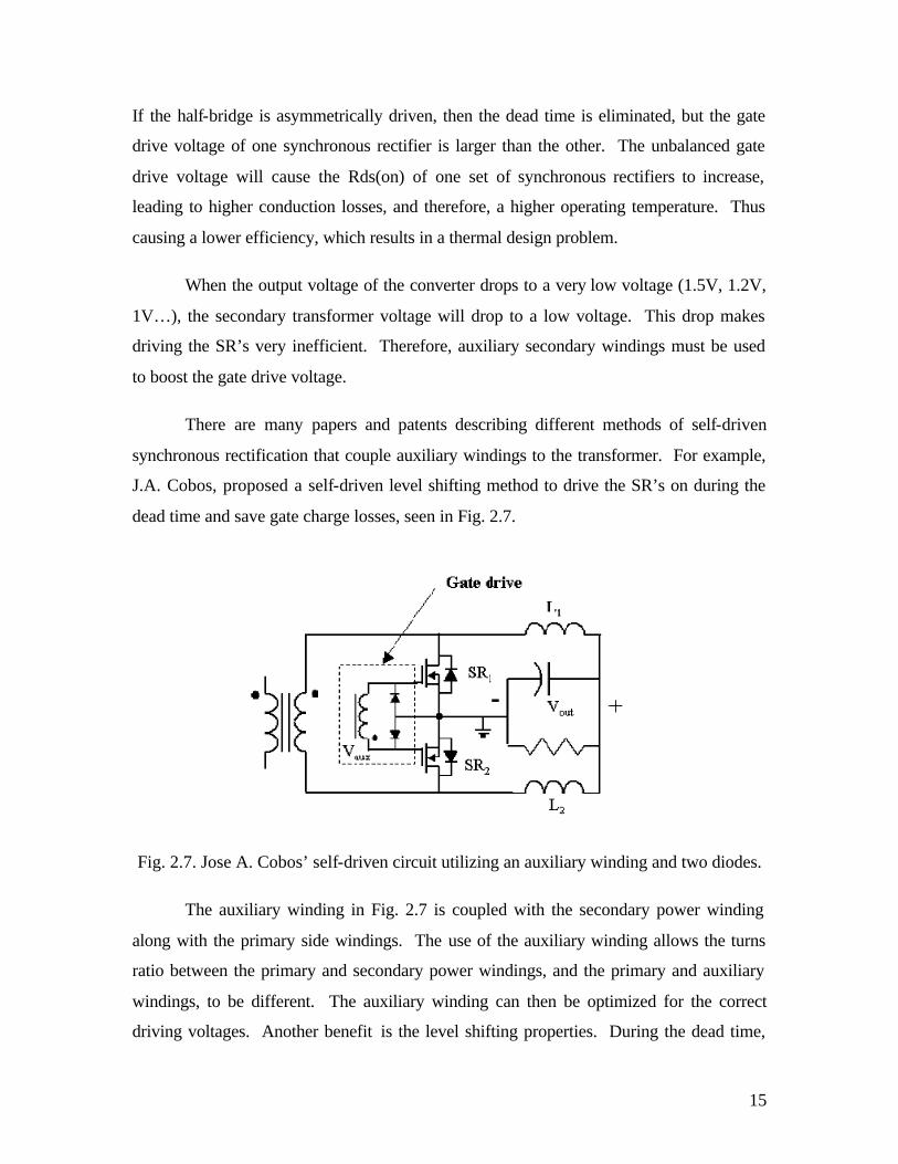
dead time and save gate charge losses, seen in Fig. 2.7.
Fig. 2.7. Jose A. Cobos’ self-driven circuit utilizing an auxiliary winding and two diodes.
The auxiliary winding in Fig. 2.7 is coupled with the secondary power winding
along with the primary side windings. The use of the auxiliary winding allows the turns
ratio between the primary and secondary power windings, and the primary and auxiliary
windings, to be different. The auxiliary winding can then be optimized for the correct
driving voltages. Another benefit is the level shifting properties. During the dead time,

16
the gate charge from one synchronous rectifier will distribute itself evenly between both
SR’s. During the freewheeling period both SR’s will turn on and the existing gate charge
will be saved. The gate drive waveforms are shown in Fig. 2.8.
Fig. 2.8. The auxiliary winding voltage and the VGS waveforms for one synchronous rectifier shown in Fig. 2.7.
In Fig. 2.8, the level shifting properties can be seen. During the freewheeling
period, the gate drive voltage is one half of the voltage during the power delivery period.
Even though both synchronous rectifiers turn on during freewheeling, the gate drive
voltage is less than optimal, leading to higher conduction losses. Also, when the primary
switch turns off, the leakage inductor of the transformer will begin to ring with the output
capacitor of the primary side MOSFET. Due to the auxiliary winding being coupled
directly with the power windings, the leakage energy in the power delivery path will
couple into the gate driver auxiliary windings. The leakage energy will then show up at
the gate of the synchronous rectifiers and cause unwanted turn-off or over voltage,
ringing at the gate. At high frequency, the chances of unwanted turn-off increase. If the
leakage energy or unwanted turn-off time is too large the synchronous rectifiers could be
damaged, or the body diode will conduct for an excessive amount of time resulting in a
lower overall efficiency. An alternate form of a self-driven gate drive circuit must be
used.
In summary, the conventional gate driver has severe losses at high frequency and
with multiple synchronous rectifiers. The resonant gate driver shows promising gate
driver savings, but at the price of added complexity. The self-driven gate driver shows
loss savings capabilities and has a simple structure, but during dead-times has the

17
possibility of shutting off. One other benefit of self-driven circuits is that the gate drive
signal is nearly instantaneous, thus reducing, or even eliminating, the body diode
conduction time.
The externally driven gate drivers need to pass the drive signal from the primary
side to the secondary side, to coordinate with the power delivery period. When the gate
drive signal arrives at the secondary side there will be an additional delay time from the
signal transmission. A possible fix would be to add an adaptive control scheme to
compensate for the signal delay time. The adaptive control will just add further
complexity to the circuit. Therefore, a simple self-driven circuit is the most
advantageous gate drive circuit to use.
2.3 Zero-Voltage-Switched Phase-Shifted Full Bridge
Referring to Fig. 2.3, the third highest frequency dependant loss at 1 MHz is the
switching loss. A form of soft switching must be used to alleviate these losses. Over the
years many different topologies using soft switching pulse width modulated (PWM) have
been proposed. The most common soft-switched PWM topology is the phase-shifted full
bridge shown in Fig. 2.9a, and the phase-shift operation is shown in Fig. 2.9b. Seen in
Fig. 2.9b, switches Q1 and Q2, as well as Q3 and Q4, are switched in a complementary
fashion with 50% duty cycle. Phase-shifting the two legs of the full bridge converter
regulates the output voltage. The first leg, containing switches Q1 and Q2, is called the
active or leading leg, and as follows the second leg, containing switches Q3 and Q4 is
called the passive or lagging leg. The leading leg gets its name from the rising edge of
the gate signal coming before, or leading, the corresponding rising edge of the lagging
leg.

18
(a)
(b)
Fig. 2.9. (a) Phase shifted full bridge topology, (b) Ideal phase-shift operation.
The phase-shift full bridge converter is widely used because of the circuit’s ability
to achieve zero-voltage-switching of all four of the primary side switches. Fig. 2.10
shows the circuit timing operation for the phase-shift full bridge.
Q1
Q2
Q3
Q4
A
B
Lk1
Lf
Q1Q2
Q3
Q4
0
VAB
Phase-Shift Operation
Q1Q2
Q3
Q4
0
VAB
Phase-Shift Operation

19
Fig. 2.10. Circuit timing operation of the phase-shift full bridge.
Starting at just before time t1, switches Q1 and Q3 are on, and zero volts are
applied across the transformer; essentially shorting out the transformer. The load current
will freewheel on the secondary side with all four diodes, in Fig. 2.9a, conducting. The
transformer leakage current will freewheel on the primary side, down through switch Q1,
and back up through switch Q3.
At time t1, switch Q3 will shut off. The leakage current in the transformer will
continue to flow, and will begin to charge and discharge the output capacitor of switch Q3
and Q4, in a sinusoidal fashion. If the leakage energy is high enough, the voltage across
switch Q3 will resonate up to the bus voltage, and the voltage across Q4 will resonant
down to zero. Switching Q4 at the precise moment when the voltage across the switch is
zero is called zero-voltage switching (ZVS). The condition for ZVS of the lagging leg is
as follows:
22
22
21
21
21
ILVCVC LKINTRINMOS ≤+ (2.2)
where CMOS is the sum of the equivalent output capacitances of the primary side switches
Q3 and Q4, VIN is the input voltage, CTR is the transformer winding capacitance, LLK is
0
VAB
t1 t2 t3 t4 t50
0
IXFMR
VSEC
I1
I2
Ip

20
the value of the leakage inductor and I2 is the leakage inductor current freewheeling in
the primary side just after Q3 turns off.
From time t2 to t3, switches Q1 and Q4 are on. Voltage is built up on the
secondary side of the transformer and the output filter gets charged.
At time t3, switch Q1 will turn off. The load current reflected through the
transformer will begin to charge and discharge the output capacitance of Q1 and Q2,
respectively. The condition for ZVS on the leading leg is as follows:
222
21
21
21
OEQINTRINMOS ILVCVC ≤+ . (2.3)
Where LEQ is the equivalent output inductor plus the leakage inductance reflected
to the primary side and IO is the reflected load current. If the load current is high enough,
the voltage across Q1 will resonate up to the bus voltage, and the voltage across Q2 will
resonant down to zero. When the voltage across Q2 is zero, the switch is turned on under
a ZVS condition.
From time t3 to t4, zero volts are applied across the transformer. The energy in the
leakage inductor will circulate through switches Q2 and Q4. Then at time t4, switch Q4
will turn off. The leakage current will then resonate again with the output capacitor of Q3
and Q4. If the condition in (2.2) is met then ZVS of switch Q3 can be realized.
Achievement of ZVS in the lagging leg (switches Q3 and Q4) is much more
difficult than in the leading leg (switches Q1 and Q2) because of the smaller amount of
energy in the system. The ZVS condition for the lagging leg is dependant on the leakage
inductor value and the square of the leakage current. Furthermore, the ZVS condition for
the leading leg depends on the sum of the leakage inductor plus the reflected output
inductor and the square of the reflected load current. Therefore, ZVS of the leading leg
can be effortlessly achieved.
There are two basic methods to make achieving ZVS of the lagging leg easier.
The first is to reduce the output capacitor of the MOSFET switch; the second requires

21
enlarging the leakage inductor value in the transformer. The output capacitor of the
MOSFET switch benefits the circuit by acting as a lossless snubber that will reduce the
turn-off losses and limit the dv/dt of the primary side switches. Therefore, the better way
to increase the ZVS range is to enlarge the effective value of the leakage inductor.
Designing a poor coupling from the primary to secondary windings, or gapping
the transformer core, can increase the effective leakage of the transformer. There are two
major drawbacks with using the transformer leakage as the main source of leakage
inductance, (a) creating a specific and repeatable leakage inductor by designing poor
coupling from primary to secondary would be very difficult if not impossible, and (b)
gapping the transformer core will significantly increase the losses associated with the
transformer. The preferred method for regulating the leakage inductance is to place a
small series inductor with the primary side windings of the transformer. The series
inductor can be optimized to achieve ZVS over almost any load range condition and the
losses and inductance can be controlled.
Enlarging the leakage inductor, or placing an inductor in series with the
transformer windings, can have a great benefit when it comes to achieving ZVS, but this
inductance comes with a penalty: loss of duty cycle. Duty cycle loss is equal to the
amount of time the freewheeling current in the resonant inductor takes to switch from
time t1 to time t2, or time t4 to t5, in Fig. 2.10. The duty cycle loss can be calculated by the
following:
]2
*)1(2[
2
TD
LV
IT
LV
nnD
O
OO
LK
IN
PS −−=∆ . (2.4)
Where T is the period and ∆D is the duty cycle loss. Duty cycle loss is
detrimental to circuits working at high frequency because the duty cycle loss is nearly
fixed. If the duty cycle loss is held constant, and the switching frequency increases, the
available time period for power delivery decreases by the amount of duty cycle loss.
Therefore, when a large duty cycle is needed, regulating the output voltage can become a
problem.

22
The time required to achieve ZVS is contained in the duty cycle loss. The period
for ZVS is easily calculated as one fourth of the resonant time of the equivalent series
inductance and the total equivalent parallel capacitance of the MOSFET switch as
follows:
1)2
1(*)
41
( −=LC
dtπ
. (2.5)
Due to the different equivalent series inductors for the lagging and leading legs,
the required time for ZVS operation is different for each leg. For the lagging leg, the
total series inductance is the equivalent leakage inductance. In the leading leg, the total
series inductor is the sum of the leakage inductance and the reflected load inductor.
Therefore, the time required for ZVS in the leading leg is much shorter than that of the
lagging leg. A dead time, corresponding to the required time for ZVS operation, is
placed between the turn-off of one switch and turn-on of the complementary switch.
Equations (2.2) and (2.3) show the condition for ZVS as an inequality. It does not
mean that there is no benefit to the phase shift full bridge if these inequalities are not met.
Partial ZVS can be achieved, as seen in Fig 2.11. Also, there is no added benefit for
exceeding the inequalities. Greatly exceeding the inequalities in (2.2) and (2.3) will lead
to an increase in the circulating energy in the system, which, in turn, increases the
conduction losses. Therefore, a trade-off between switching losses and conduction losses
must be made. The load condition that ZVS is achieved must be decided.
(a) (b) (c)
Fig. 2.11. (a) Full ZVS operation, (b) ZVS met, extra circulating energy (c) Partial ZVS,
not enough energy to meet ZVS requirement.
dt dtdtdt dtdt

23
2.4 Complementary-Controlled Full Bridge with a Current-Doubler
At higher switching frequencies the phase-shifted full bridge is an excellent
choice because of its soft-switching capabilities. At higher output currents and lower
output voltages, the current doubler rectifier with synchronous rectification is superior,
though using the combination of the phase-shift full bridge and the current doubler
rectifier does not lead to an easy implementation of self-driven synchronous rectification.
The desire to use a self-driven scheme is previously explained. However, with a
modification in the control strategy of the phase-shifted full bridge, the lesser-known
complementary-controlled full bridge can be derived, as seen in Fig. 2.12.
Fig. 2.12. Comparison of the phase-shift and the complementary control operations.
The operation of the complementary-controlled full bridge is nearly the same as
the phase shift controlled full bridge, except that the duty cycle is formed by a controlled
switch rather than phase-shifting the two legs of the converter. The complementary-
control full bridge with the current doubler secondary is depicted in Fig. 2.13. From the
complementary control diagram in Fig. 2.12 and Fig. 2.13, switches Q2 and Q4 are the
duty cycle control switches and Q1 and Q3 are the freewheeling switches.
Q1
Q2
Q3
Q4
0
VAB
Phase-Shift Operation
Q1
Q2
Q3
Q4
0
VAB
Phase-Shift Operation
Q1
Q2
Q3
Q4
0
VAB
Complementary Control Operation

24
Fig. 2.13. The complementary-control full bridge with a current-doubler secondary side.
The freewheeling switches Q1 and Q3 are both turned on for greater than one half
of the switching period. If the situation was reversed and Q1 and Q3 were the control
switches while Q2 and Q4 were the freewheeling switches, the complementary-controlled
operation would be preserved. For the duration of this work, Q2 and Q4 will be the
referred to as the control switches and Q1 and Q3 as the freewheeling switches.
The full circuit operation of the complementary-control full bridge with the
current doubler secondary can be seen in Fig. 2.14.
Just before time t0, the primary side of the circuit has switch Q1 on and all other
primary switches are off. On the secondary side both synchronous rectifiers, S1 and S2,
are also on, however, S1 is beginning to turn off. The output inductor current in LF1 is
freewheeling through S1 and LF2 is freewheeling through S2. The current in the leakage
inductor LK1 is freewheeling through both S1 and S2, and then returns through the
transformer. Meanwhile, the leakage current is charging the output capacitance of Q3 and
discharging that of Q4.
+-
Q1
Q2
Q3
Q4
A
B
Lk1
S1
S2
LF1
LF2
Vout
+-
Q1
Q2
Q3
Q4
A
B
Lk1
+-
Q1
Q2
Q3
Q4
A
B
Lk1
S1
S2
LF1
LF2
Vout

25
Fig. 2.14. Operation of the complementary-controlled full bridge with the current-
doubler secondary side.
At time t0, the switch Q4 turns on and S1 is turned off. If the energy stored in the
leakage inductor, at time t0, is large enough to discharge the output capacitance of Q4 to
zero, then ZVS operation is achieved. The condition for ZVS of switch Q4 is identical to
the condition for ZVS for the lagging leg in the phase-shift full bridge, given in (2.2). At
the turn on of Q4, the bus voltage is placed across the transformer and the leakage
inductor. Once the leakage inductor current changes direction, power is delivered to the
secondary side and LF1 begins to charge. The power delivery will continue to until time
t1 and S2 conducts the full load current. One half of the load current is delivered from the
primary side and the other half is from the discharge of the filter inductor, LF2.
At time t1, the power delivery period is over; Q4 begins to turn off and S1 begins
to turn back on. The current in the leakage inductor at this point is equivalent to the peak
inductor ripple current in LF1. The current in LF2 will continue to freewheel through S2.
Once Q4 turns off, the reflected filter inductor current in LF1 begins to charge the output
capacitance of Q4 and discharge that of Q3. If the circulating energy is large enough to
VGS(Q1)
VGS(Q2)
VGS(Q3)
VGS(Q4)
VAB
Complementary Control Operation
0
0
0
0
0
IS0
VA 0
0VB
VGS(S1)
VGS(S2)
0
0
t0 t1 t2 t3 t4 t5 t6

26
charge the output capacitor of Q4 to the bus voltage, then ZVS of Q3 is achieved. The
condition for ZVS of Q3 is equivalent to that of the leading leg in the phase-shift full
bridge, given in (2.3). Because the secondary stage is the current doubler the load
current, I0 represented in (2.3) is only one half of the full load current.
From time t1 to t2, the resonant action between the output capacitors of switches
Q3 and Q4 and the reflected filter inductor takes place. At time t2, switch Q3 and S1 turn
on and the freewheeling period begins. The current in the leakage inductor freewheels
around the primary side through switch Q1, through the transformer and back through
switch Q3. The load current will freewheel through S2, and the current in the leakage
inductor LK1 will freewheel through both S1 and S2 and return through the transformer.
At time t3, switch Q1 will turn off. The leakage inductor will begin to charge and
discharge the output capacitors of Q1 and Q2, respectfully.
At time t4, switch Q2 will turn on and S2 will turn off. Again, if the leakage
inductor energy is adequate, then ZVS of Q2 can be achieved. The conditions for ZVS of
Q2 is the equivalent to that of Q4 and (2.2). Because Q3 and Q2 are both on, the bus
voltage is applied across the transformer and the leakage inductor. Once the leakage
current changes direction, power is supplied to the secondary side until time t5. One half
of the load current is delivered from the primary side charging LF2 and the other half is
from the discharge of the filter inductor LF1. Switch S1 will carry the full load current.
Right at time t5, switch Q2 will turn off and S2 will begin to turn on. The output
capacitor of Q2 and Q1 will charge and discharge, respectfully, by the reflected current in
LF2. A resonant action will occur between the output capacitor of Q1, Q2 and the
reflected output inductor.
At time t6, the switch Q1 will turn on. If the circulating energy is large enough to
charge the output capacitor of Q2 to the bus voltage, then ZVS of Q1 is obtained. The
condition for ZVS of Q1 is the same as that for Q3.
From the previous analysis, the top switches Q1 and Q3 correspond to the leading
leg in the phase-shift full bridge, while Q2 and Q4 correspond to the lagging leg. As
27
follows, ZVS can be achieved for each of the four switches. However, ZVS is harder to
achieve in the control switches. The methods reported in section 2.3 for improving the
ZVS range, as well as, all other prior methods for extending the ZVS range can be
applied to the complementary-controlled full bridge.
Although the complementary-controlled full bridge has the same basic
characteristics at the phase-shift full bridge, there is one added benefit that is an easy
implementation for self-driven synchronous rectification.
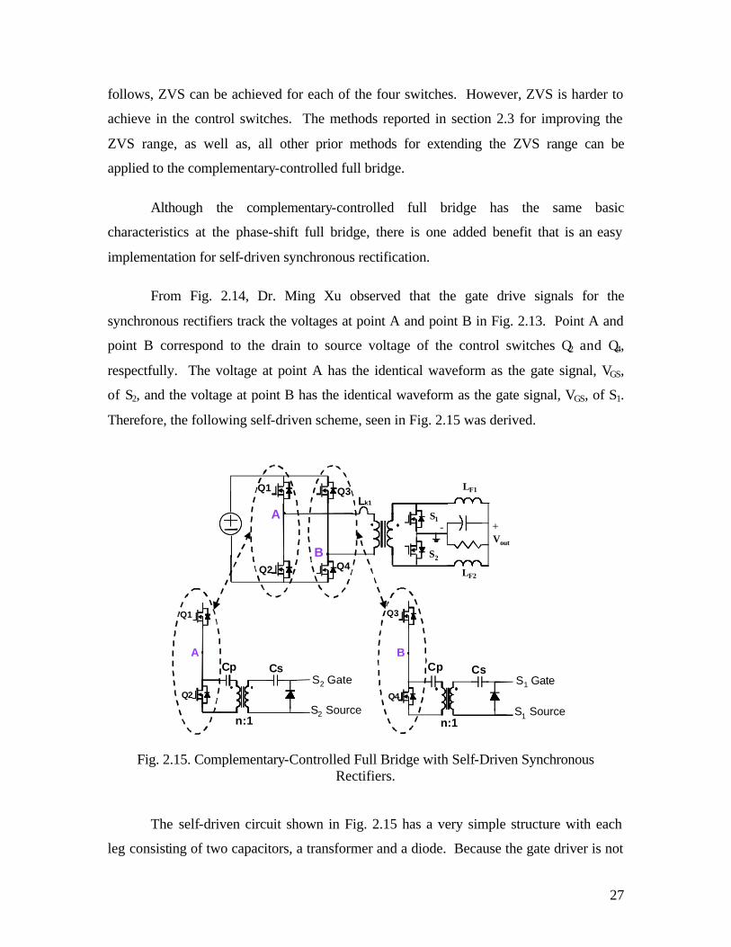
From Fig. 2.14, Dr. Ming Xu observed that the gate drive signals for the
synchronous rectifiers track the voltages at point A and point B in Fig. 2.13. Point A and
point B correspond to the drain to source voltage of the control switches Q2 and Q4,
respectfully. The voltage at point A has the identical waveform as the gate signal, VGS,
of S2, and the voltage at point B has the identical waveform as the gate signal, VGS, of S1.
Therefore, the following self-driven scheme, seen in Fig. 2.15 was derived.
Fig. 2.15. Complementary-Controlled Full Bridge with Self-Driven Synchronous
Rectifiers.
The self-driven circuit shown in Fig. 2.15 has a very simple structure with each
leg consisting of two capacitors, a transformer and a diode. Because the gate driver is not
Q1
Q2
A
S2 Gate
S2 Source
Cp
n:1
Q3
Q4
B
S1 Gate
S1 Source
Cp
n:1
+-
Q1
Q2
Q3
Q4
A
B
Lk1
S1
S2
LF1
LF2
Vout
Cs Cs

28
coupled to the power transformer, the synchronous rectifiers are able to track the primary
side voltages at point A and B very quickly and the signals have a very clean waveform.
2.5 Steady-State Operation of the Proposed Self-Driven Scheme
The preceding sections presented the different secondary side rectifier topologies,
the differences between external and self-driven synchronous rectifier gate drivers, and
derived a new method for self-driven synchronous rectification. In this section, the
operation of the proposed self-driven scheme is presented.
As discussed previously, at high frequencies the gate driver and body diode losses
of the synchronous rectifiers combine to be the most significant portion of the overall
losses. However, improving the gate drive speed and timing, as well as, utilizing loss
saving gate drive techniques can significantly reduce these losses. The proposed self-
driven circuit can save gate-driving losses and significantly reduce the body diode
conduction time and losses.
To facilitate the basic operation of the self-driven circuit, Fig. 2.16 shows the path
of the gate drive current during a completely non-ZVS condition for the turn-on and turn-
off of the synchronous rectifiers.
(a) (b)
Fig. 2.16. Path of the gate drive current during complete non-ZVS (a) turn on and (b)
turn off of the synchronous rectifiers.
Q1
Q2
Cp
n:1
Cs
VBUS
CGS
SR
D1
++
--
Q1
Q2
Cp
n:1
Cs
VBUS
CGS
SR
D1
++ -
-

29
Starting from the initial turn on of the circuit, all capacitor voltages are zero. The
voltage of the primary side capacitor CP is a function of the duty cycle and the input
voltage as follows:
)1(* DVV INCP −= . (2.6)
The secondary side capacitor CS voltage is a function of the primary side
capacitor voltage of CP and the turns ratio as follows:
DCP
CS Vn
VV −= . (2.7)
Where VD is the forward voltage drop of the diode D1.
Fig. 2.17. Operating waveforms for the self-driven circuit under a non-ZVS operating
condition.
For a non-ZVS condition of the primary switches, the turn-on of the synchronous
rectifiers begins when the top switch Q1 turns on at time t1. The operating waveforms are
shown in Fig. 2.17. The bus voltage is then applied across the capacitor CP and the
primary windings of the gate drive transformer. The voltage across the primary side gate
drive windings is equal to the bus voltage minus the voltage of CP. On the secondary side
VCP
VXFMR
VCS
VGS(SR)
)1(* DVIN −
DCP Vn
V−
t1 t2
0
0
0
0

30
of the gate drive transformer, the gate voltage of the synchronous rectifiers is equal to the
secondary gate drive transformer voltage added with the series voltage of CS.
The turn-off of the synchronous rectifiers is initiated with the turn-on switch Q2 at
time t2. The capacitor voltage of CP is then applied across primary winding. The voltage
of CP is reflected to the secondary side of the transformer. Therefore, the gate voltage of
the synchronous rectifiers will equals VCP / n – VCS, which results in a negative voltage
equal to the forward voltage drop of D1 being applied to the gate of the synchronous
rectifiers. Therefore, the synchronous rectifiers will turn-off. During a non-ZVS process
of the primary switches all of the synchronous rectifier gate charge is lost. However,
when the self-driven scheme is used in conjunction with a ZVS mode of operation the
gate drive losses can be saved.
The key ZVS operating waveforms of the complementary-controlled full bridge
with self-driven synchronous rectifiers are shown in Fig. 2.18 and the topological stages
are shown in Fig 2.19 through Fig. 2.24.
Fig. 2.18. Key operating waveforms for the self-driven complementary-controlled full bridge detailing one switching cycle of the self-driven circuit.
VGS(Q1)
VGS(Q2)
VGS(Q3)
VGS(Q4)
VAB
0
0
0
0
0
IS0
VA 0
0VB
VGS(S1)
VGS(S2)
0
0
t0 t1t2 t3 t4 t5

31
The converter is in a freewheeling state just before time t0, Fig. 2.18. At time t0,
Q1 turns on. Both of the output synchronous rectifiers and the primary side top switches
Q1 and Q3 are now on. The energy stored in the transformer leakage inductor and/or
primary side series inductor is freewheeling, and is represented as LEQ in Fig. 2.19. The
total energy in LEQ, just before time t0, is equivalent to the current in the filter inductor,
LF2. At this time the current in LF2 is as follows:
S
OLF F
DIi
*2)1(
22
−+= . (2.8)
Although both synchronous rectifiers are on, S1 will carry the entire load current
consisting of I2 and I3 in Fig. 2.19 and S2 will carry no current. The voltage across the
primary side of the transformer is zero, essentially a short circuit. Just after time t0, until
t1, the current in the leakage inductor begins to linearly decrease causing a difference in
current shared between the leakage inductor and LF2.
Fig. 2.19. Topological stage for the self-driven circuit at time t0.
At time t1, in Fig. 2.18 and 2.20, switch Q3 begins to open. The leakage energy
will begin to charge the output capacitor C3 of Q3 and discharge the output capacitor C4
Q3
Q4Cp
n:1
CsCGS
S1
D1
LEQ
Q1
Q2
SS11
SS22
A B
I1
I2
I2
+
-
I3
I3

32
of Q4. As a result, the voltage at point B, which corresponds to the drain-to-source
voltage of Q4, is discharged to zero. The leakage inductor LEQ will begin to turn off the
synchronous rectifier S1, and if ZVS occurs, the gate charge of S1 is recovered. From a
circuit point, of view the input capacitor of switch S1 is effectively in parallel with C4,
acting as a lossless snubber. The current in the leakage inductor during ZVS is as
follows:
bbaLEQ IIIIi 5111 ++== (2.9)
Where the currents I1, I1a, I1b, and I5a are depicted in Fig. 2.20.
Fig. 2.20. Topological stage for the self-driven circuit at time t1.
From time t1 to t2, the resonant action between the leakage inductor and the
parallel combination of C3, C4 and Cgs (S1) occurs. The time t2 occurs at one fourth of the
resonant period. The energy needed to obtain ZVS is as follows:
2
2 )(21
INGS
MOSZVS Vn
CCE += . (2.10)
If the energy given in (2.10) is exceeded, before time t2, then the body diode of Q4
will begin to conduct and essentially zero volts are across Q4. Then ZVS can be
obtained. However, during the body diode conduction time of Q4, the synchronous
Q3
Q4
Cp
n:1
Cs CGS
S1
D1
LEQ
Q1
Q2
SS11
SS22
A B
I1
I2
I2
+
-
I3
I3
I4
I1a
I1b I5aI5b
LF2
LF1
C4
C3

33
rectifier S1 is turned off, allowing the body diode of S1 also to conduct. Having the body
diode of S1 conduct is detrimental to the overall efficiency of the circuit. Therefore, the
body diode conduction time of Q4 and S1 must be minimized.
At time t2, Q4 is closed, as seen in Fig. 2.21. If the ZVS operation was met then
S1 was already turned off. However, if ZVS was not met, then switch S1 will begin to
turn off. Assuming a non-ZVS situation, once Q4 turns off, the voltage of CP will apply
across the gate drive transformer. The negative voltage of CP will reflect to the
secondary side. Because the voltage of CS is a function of CP and the turns ratio, given in
(2.6) and (2.7), then the voltage applied to CGS will be D1. To have fast conduction of D1
a Schottky diode is used. The typical forward drop of the Schottky diode is 0.3 V.
Therefore, S1 will turn off.
Fig. 2.21. Topological stage for the self-driven circuit at time t2.
From time t2 to t3, the bus voltage is applied across the primary side of the
transformer. The current in the leakage inductor is forced to change directions. Once the
leakage inductor changes direction, power is delivered to the secondary side at time t3.
The inductor LF1 then begins to charge and S2 conducts the full load current. If during t2
to t3, switch S1 is not fully turned off, a shoot through current can occur. The timing
issues and occurrences of the shoot through current are discussed in the following
section.
Q3
Q4Cp
n:1
Cs CGS
S1
D1
LEQ
Q1
Q2
SS11
SS22
A B
I1
I2
I2
I3
I3
I4
I1
LF2
LF1

34
At time t3, the voltage of CS will track CP according to (2.7). This current is
shown in Fig. 2.22 as I3a and I3b.
Fig. 2.22. Topological stage for the self-driven circuit at time t3.
At time t4, the power delivery period ends by Q4 turning off. From time t4 to t5,
the reflected current in LF1, represented as I1 in Fig. 2.23, charges and discharges the
capacitors C4 and C3, respectfully. Point B follows the drain-to-source voltage of Q4. As
Point B resonates up to the bus voltage, a positive voltage is applied across the gate drive
transformer. Then I1 will also begin to charge the gate of S1.
Fig. 2.23. Topological stage for the self-driven circuit at time t4.
Q3
Q4
Cp
n:1
Cs CGS
S1
D1
LEQ
Q1
Q2
SS11
SS22
A B
I1
I2
I4
I3aI3b
LF2
LF1
Q3
Q4Cp
n:1
Cs CGS
S1
D1
LEQ
Q1
Q2
SS11
SS22
A B
I1
I2
I4I1a
I1bI3a I3b
LF2
LF1
C4
C3

35
Time t5 is tuned to occur precisely at one fourth of the resonant time of the
reflected filter inductor LF1, the parallel combination of C3, C4, and the reflected input
capacitance of S1. If ZVS is obtained, then the circulating current in the circuit turns on
S1. The required energy for ZVS is given in (2.10).
Under a non-ZVS condition at time t5 the voltage at point B is raised to the bus
voltage by means of Q3. Therefore, the bus voltage less the voltage of CP is applied
across the gate drive transformer. On the secondary side, the series voltage of CS and the
secondary gate drive voltage are placed across the gate to source of S1. Then, S1 is turned
on.
Once Q3 is turned on, the circuit begins a freewheeling state with Q1, Q3 and both
synchronous rectifiers on. At time t5, shown in Fig. 2.24, the leakage inductor current I1
freewheels on the primary side, and on the secondary side, S2 carries the full load current.
After time t5, the leakage current begins to dissipate and the switch S1 begins to carry the
difference between the filter inductor current in LF1 and the leakage current.
Fig. 2.24. Topological stage for the self-driven circuit at time t5.
Q3
Q4Cp Cs CGS
S1
D1
LEQ
Q1
Q2
SS11
SS22
A B
I1
I2
I3
+
-
LF2
LF1

36
2.6 Transient Operation of the Self-Driven Scheme
The preceding section presented the operation of the self-driven scheme
neglecting the transient operation and the effects of the parasitic components in the self-
driven circuit. In this section, the parasitic components are taken into account in a further
examination of the self-driven circuit.
Fig. 2.25. Self-driven gate drive circuit with damping resistor.
The addition of the transformer leakage and parasitic trace inductances causes an
oscillation between the leakage inductors and the gate capacitor of the synchronous
rectifiers. An additional gate resistor Rg is used to dampen these oscillations, seen in Fig.
2.25.
During a ZVS turn on of a top switch, the reflected load current will charge the
equivalent primary side snubber capacitor and the gate capacitor of the synchronous
rectifier. During a ZVS turn on of a bottom switch, the leakage inductor of the main
transformer will discharge the equivalent primary side snubber capacitor and the gate
capacitor of the synchronous rectifier. The equivalent self-driven circuit diagram during
turn-on and turn-off of the synchronous rectifiers is shown in Fig. 2.26.
From the circuit diagrams, it is shown that the self-driven circuit acts as a current-
source driver during turn-on and a resonant type during turn-off. In actuality, during
turn-on the current source in Fig. 2.26a is the reflected filter inductor, which has very
high impedance, and therefore, can be modeled as a constant current source. The
Q1 (Q3)
A (B)
S1(S2) Gate
S1(S2) Source
Rg
Cr
n:1 Lk2
Q2 (Q4)
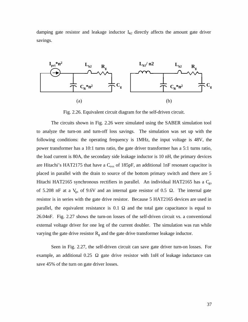
37
damping gate resistor and leakage inductor Lk2 directly affects the amount gate driver
savings.
(a) (b)
Fig. 2.26. Equivalent circuit diagram for the self-driven circuit.
The circuits shown in Fig. 2.26 were simulated using the SABER simulation tool
to analyze the turn-on and turn-off loss savings. The simulation was set up with the
following conditions: the operating frequency is 1MHz, the input voltage is 48V, the
power transformer has a 10:1 turns ratio, the gate driver transformer has a 5:1 turns ratio,
the load current is 80A, the secondary side leakage inductor is 10 nH, the primary devices
are Hitachi’s HAT2175 that have a Coss of 185pF, an additional 1nF resonant capacitor is
placed in parallel with the drain to source of the bottom primary switch and there are 5
Hitachi HAT2165 synchronous rectifiers in parallel. An individual HAT2165 has a Cgs
of 5.208 nF at a Vgs of 9.6V and an internal gate resistor of 0.5 Ω. The internal gate
resistor is in series with the gate drive resistor. Because 5 HAT2165 devices are used in
parallel, the equivalent resistance is 0.1 Ω and the total gate capacitance is equal to
26.04nF. Fig. 2.27 shows the turn-on losses of the self-driven circuit vs. a conventional
external voltage driver for one leg of the current doubler. The simulation was run while
varying the gate drive resistor Rg and the gate drive transformer leakage inductor.
Seen in Fig. 2.27, the self-driven circuit can save gate driver turn-on losses. For
example, an additional 0.25 Ω gate drive resistor with 1nH of leakage inductance can
save 45% of the turn on gate driver losses.
Lk2 Rg
CR*n2 Cg
Ipri*n2 Lk2 Rg
CR*n2 Cg
Lk1/ n2

38
Fig. 2.27. Turn on loss comparison of the self-driven circuit vs. a conventional external
voltage driver, both operating at 1MHz for 5 HAT2165 in parallel.
Fig. 2.28 shows the turn-off losses of the self-driven circuit vs. a conventional
external voltage driver. The simulation was run while varying the gate drive resistor Rg
and the gate drive transformer leakage inductor.
Fig. 2.28. Turn-off loss comparison of the self-driven circuit vs. a conventional external
voltage driver, both operating at 1MHz for 5 HAT2165 in parallel.
Seen in Fig. 2.28, the self-driven circuit can save gate driver turn-off losses. For
example an additional 0.25 Ω gate drive resistor with 1nH of leakage inductance can save
50% of the turn-off gate driver losses. During turn-off, the equivalent gate drive circuit is
a resonant circuit. The gate driver losses below a 0.2 Ω gate resistor actually begin to
Gate Driver Loss Comparison During Turn-On
0
0.2
0.4
0.6
0.8
1
1.2
1.4
0.1 1 10
Gate Resistor(Ohms)
Po
wer
Dis
sip
atio
n (
W)
Leakage = 1nH Leakage = 3nH
Leakage = 5nH Conventional Voltage Driver
Gate Driver Loss Comparison During Turn-off
0
0.20.4
0.6
0.8
1
1.2
1.4
0.1 1 10
Gate Resistor (Ohms)
Po
wer
Dis
sip
atio
n (W
)
Leakage = 1nH Leakage = 3nH
Leakage = 5nH Conventional Voltage Driver

39
increase, but remain below the conventional external driven circuit. For example in the
5nH leakage inductor case the losses at 0.1 Ω are about 1.1W while 0.95W at 0.25 Ω.
During a turn-off transition, the leakage inductor Lk2, shown in Fig. 2.25, is
charged by the gate capacitance of the synchronous rectifiers. Once the synchronous
rectifier gate to source voltage drops below the forward voltage of the source-to-gate
diode, the leakage inductor will charge CS beyond the secondary side of the gate drive
transformer voltage. If the leakage inductor charges CS beyond the secondary side of the
gate drive transformer voltage, the difference can possibly reach the threshold voltage of
the synchronous rectifiers. If the synchronous rectifier turns back on, there will be a
simultaneous conduction of both synchronous rectifiers and a short circuit will occur. An
example of this process is shown in Fig. 2.29.
Fig. 2.29. Test waveforms of a self-driven complementary-controlled full bridge
operating at 650 kHz. (top waveform) VGS of a synchronous rectifier, (bottom waveform) voltage across a 0.5 Ω gate drive resistor.
Depicted in Fig. 2.29 are test waveforms of a self-driven complementary-
controlled full bridge operating at 650 kHz. The synchronous rectifiers are 5 HAT2165
from Hitachi placed in parallel. Circled in the top waveform of Fig. 2.29 is the turn-off
period of the synchronous rectifier. The gate voltage drops below negative 0.7 V and
then is brought back to near positive 2-volts. For example, if the threshold voltage of the
synchronous rectifier is less than 2-volts, then the switch will turn back on.

40
Another possibility for the VC2 to be greater than the secondary side gate drive
transformer voltage is during a transient. In a steady state operation, VCS will follow the
reflected voltage of CP. The voltage of CP given in (2.6) is duty cycle and input voltage
controlled. During turn off, the voltage of CP controls the secondary side gate drive
transformer voltage. In a steady state operation, the secondary side gate drive voltage
equals VCS that turns off the SR’s. If VCS is less than the secondary side gate drive
transformer voltage, CS is charged through a forward biased diode to equal the secondary
side gate drive voltage. During a transient, if the load current is increased or the input
voltage is decreased, the duty cycle will enlarge. Then the secondary side gate drive
transformer voltage will decrease to less than VCS. Because there is not a low resistance
path for CS to discharge during a transient, a net positive voltage will be left at the gate of
the synchronous rectifiers. Therefore, if the voltage difference is greater than the
threshold voltage of the synchronous rectifier, then the synchronous rectifier will not turn
off causing a secondary side shoot through current.
To make CS rapidly track CP, a low resistance path is needed. Therefore, the
diode in Fig. 2.25 is replaced by a tiny MOSFET, shown in Fig. 2.30. An additional
winding is coupled to the gate drive transformer to control the tiny MOSFET.
Fig. 2.30. Self-driven circuit with the additional tiny MOSFET.
With the addition of the tiny MOSFET, CS will track CP, but now a path is formed
for the leakage inductor Lk2 to freely oscillate, as shown in Fig. 2.31. Circled in Fig. 2.31
Q1 (Q3)
A (B)
S1(S2) Gate
S1(S2) Source
Rg
Cr
n:1 Lk2
Q2 (Q4)
CP CS

41
is the leakage inductance oscillation, as the tiny MOSFET turns on. The potential
problem with having a fast turn on of the tiny MOSFET is that the resonant peak of the
oscillations could cross the threshold of the synchronous rectifier. If the threshold is
reached, there will be a secondary side shoot through current. Therefore, the timing of
the tiny MOSFET is critical.
If the tiny MOSFET does not turn off before the synchronous rectifiers are to turn
on, then the synchronous rectifier turn on signal is shorted to ground through the tiny
MOSFET. In this case, because the turn on of the synchronous rectifiers is under a
virtual ZCS situation, the synchronous rectifier turn on speed is not too critical.
If the tiny MOSFET turns on before the ZVS action of the primary switches
completely discharges the gate of the synchronous rectifiers, the gate drive loss savings
will be reduced. Likewise, under a non-ZVS condition having the tiny MOSFET turn on
quickly will reduce the potential for a secondary side shoot through current due to a slow
SR turn off speed.
Fig. 2.31. Test waveforms of a self-driven complementary-controlled full bridge operating at 650 kHz. (top waveform) VGS of a synchronous rectifier, (middle waveform) VGS of the tiny MOSFET, (bottom waveform) voltage across a 0.5 Ω gate drive resistor.
To completely recover all of the possible gate drive losses, a delay must be added
in the tiny MOSFET gate drive path. To allow for the tiny MOSFET to turn off quickly,
there must be a low resistance discharge path. Therefore, the following gate drive circuit,
seen in Fig. 2.32, was designed to take advantage of these properties. A 200-Ohm
Vgs(SR)Vgs(tiny)
Igate
Vgs(SR)Vgs(tiny)
Igate

42
resistor is added in the gate drive path to slow down the turn on and a Schottky diode is
placed in parallel to achieve a fast turn-off. The tiny MOSFETs used are Si3900 from
Siliconix Inc.
Fig. 2.32. Self-driven gate drive circuit with a delay in the tiny MOSFET gate drive path.
Seen in Fig. 2.33 are the operational waveforms of the self-driven circuit shown
in Fig.2.32. Circled are the gate drive turn-on and turn-off of the tiny MOSFET and the
turn-off time of the synchronous rectifiers. The slope of the turn-on of the tiny MOSFET
is very slow and the turn-off is very rapid. There are nearly no oscillations during the
turn-off time of the synchronous rectifiers. Also shown in Fig. 2.33 is the gate drive
current. The peak and shape during the turn-off of the synchronous rectifiers is nearly
equivalent to the turn-on current. Having the peak and shape equivalent shows that there
is no gate drive energy dissipated in the tiny MOSFET.
Using the gate driver shown in Fig. 2.32 has the advantages of recovering the
most possible gate drive energy. However, the addition of a slow tiny MOSFET can be
non-advantageous under light load or non-ZVS conditions. The leakage inductor in the
main power transformer dictates the timing of the tiny MOSFET.
Q1 (Q3)
A (B)
S1(S2) Gate
S1(S2) Source
Rg
Cr
n:1 Lk2
Q2 (Q4)
CP CS

43
Fig. 2.33. Operational waveforms of the self-driven circuit shown in Fig. 2.32.
The current in the main power transformer passes from a positive to a negative
direction, or vise-versa, to begin each power delivery period, shown in Fig. 2.18. The
slope of this transition is given by (2.11).
2* nLV
slopeK
IN= . (2.11)
Where LK is the leakage inductance referenced to the secondary side of the
transformer and n is the turns ratio.
If the synchronous rectifier turns off after the main power transformer current
changes direction, the current delivery path on the secondary side will be a short circuit.
Therefore, there will be a shoot through current and the losses will rapidly increase.
If the synchronous rectifier turns off before the transformer current has changed
directions, then the body diode will conduct. The time in which the transformer current
changes direction is as follows:
LK
IN
SFLK
OO
O
nLV
TDLL
Vi
I
t*)1(
)(2 1
−+
−∆+=∆ (2.12)
Vgs(SR)
Igate
Vgs(tiny) Vgs(SR)
Igate
Vgs(tiny)

44
where ∆iO is the change in output filter current, LLK is the leakage inductor seen on the
secondary side, LLF1 is one filter inductor, D is the duty cycle, and Ts is the switching
period.
Fig. 2.34 compares the operational waveforms between phase-shifted and
complementary-controlled full bridge circuits. Because the self-driven gate drive signals
respond directly to the points A and B on the primary side, the self-driven
complementary-controlled full bridge has a shorter body diode conduction time than the
phase-shifted full bridge. The body diode conduction loss comparison can be seen in Fig.
2.35, under a load condition of 1.2V/80A at 1MHz switching frequency with 10 nH
leakage inductor and a 20 ns delay time. The loss saving is 2.56 W, which is a 34%
reduction, and corresponds to a 2.5% total efficiency improvement.
(a) (b)
Fig. 2.34. Comparison between the body diode conduction times (a) Phase-shift full bridge, (b) Self-Driven complementary-controlled full bridge. Highlighted are the body
diode conduction times.
0VAB
0
0
0
0
IS
Vgs(S1)
IS1
ID(S1)
0VAB
0
0
0
0
IS
Vgs(S1)
IS1
ID(S1)
td
Io / 2
Io
Io
0VAB
0
0
0
0
IS
Vgs(S1)
IS1
ID(S1)
Io / 2
Io

45
Fig. 2.35. Body diode conduction loss comparison.
Fig. 2.36 compares the efficiency of the self-driven complementary-controlled
full-bridge with a fast tiny MOSFET and delayed tiny MOSFET depicted in Fig. 2.32.
As can be seen the efficiency under the light load conditions (pre-ZVS) the converter
with a fast tiny MOSFET has improved efficiency. After ZVS is achieved, both
converters have nearly identical efficiencies.
Fig. 2.36. Efficiency comparison of the self-driven circuit with a fast tiny MOSFET and a delayed tiny MOSFET operating 650 kHz with an output of 1.2V and an input of 48V.
Therefore, to improve the light load efficiency a faster turn-off speed for the
synchronous rectifiers is needed.
0
2
4
6
8
Loss (W)
Body Diode Conduction Loss Comparison
Loss (W) 5.022 7.582
self-driven FB Phase Shift FB
Efficiency vs. Load
77787980818283848586
0 20 40 60 80 100
Load current
Eff
icie
ncy
No resitor in series w/ tiny 200 ohm resistor in series

46
2.7 Summary
This chapter presents and analyzes a self-driven gate drive concept used on a
complementary-controlled full bridge circuit. The self-driven circuit shows a great
improvement over the conventional external driven circuit. The simplicity, loss savings
and small size of the self-driven topology lends itself to compact high-frequency isolated
DC/DC conversion. With a 0.25-Ohm gate drive resistor and an operating frequency of
1MHz, while driving 5 HAT2165 synchronous rectifiers, on each leg of the current
doubler, there is almost 50% gate driver loss savings compared to a conventional external
driver. This is a 2.5 W reduction. When comparing the phase-shift to the self-driven
complementary-controlled full bridge, the body diode loss savings are about 34%, a 2.56
W savings. Therefore, using the self-driven complementary-controlled full bridge for a
48V to 1.2V/80A, operating at 1MHz, there is a 5.1% efficiency improvement over the
phase-shifted full bridge operating under the same conditions.
The presented self-driven topology has the following beneficial attributes:
Ø The self-driven topology holds the synchronous rectifiers to the full gate
drive voltage during dead times on the power transformer
Ø The input gate capacitance of the synchronous rectifiers operates a
lossless snubber capacitor for the primary side switches
Ø 50% gate drive savings compared to an external driver
Ø Minimized synchronous rectifier body diode conduction time
Ø Very clean synchronous rectifier gate drive signals due to tight coupling
of the gate drive windings.
Ø The gate drive windings are not coupled to the power windings.
Therefore, the power windings can be optimally wound, which minimizes
the leakage inductor and the secondary side winding resistance by
utilizing all layers of the PCB for power windings. Also there are discrete

47
gate drive transformers that do not allow the power winding leakage
current to couple into the gate drive windings.

48

49
Chapter 3
Performance Improvements of Integrating Multiple
Transformers
The previous chapter illustrates a novel technique for adapting a self-driven
scheme to the complementary-controlled full bridge topology. However, with the
addition of two gate driver transformers, the implementation of the self-driven circuit
does not lead to an overall compact design. This chapter presents an integrated
transformer concept that can be used to reduce circuit complexity, the overall size and
cost of the power stage. In addition, this concept increases the efficiency of the circuit.
3.1 Motivation
In Chapter 2, the self-driven scheme used to drive the synchronous rectifiers was
adapted to the complementary-controlled full bridge. The implementation of the self-
driven circuit gave an additional two transformers that increased the circuit’s magnetic
core number to five, of which these are three transformers and two output filter inductors.
Normally, a designer uses a self-driven circuit not only for the loss saving abilities but
also for the size reduction. The addition of two gate drive transformers can reduce the
attractive properties of the self-driven circuit discussed in Chapter 2.
In a compact DC/DC converter, size is always a driving factor and the thermal
dissipation is always the limiting factor. A modular DC/DC converter, such as a VRM or
brick type converter, has a fixed form factor. For example, in designing a quarter brick
all of the electrical requirements must be placed into a standardized 1.45 inches x 2.3

50
inches x 0.452 inches for the width, length and height, respectfully. The quarter brick
also has isolation requirements, temperature limitations, standard input and output pin
placements, as well as many other design specifications. The mechanical diagram for a
PowerQor Tera PQ60012QTA40 Quarter-Brick from Synqor is shown in Fig. 3.1 and as
seen the placement of the transformers and output filter inductors is critical.
(From Synqor’s PQ60012QTA40 datasheet www.synqor.com ) Fig. 3.1. Mechanical Diagram of a PowerQor Tera PQ60012QTA40 Quarter-Brick from
Synqor.
Shown in Fig. 3.1, there are three large magnetic components. Synqor’s patented
topology shown in Fig. 3.1, is a two-stage design where the first stage acts as a current
source and the second stage is a self-driven push-pull topology with two transformers that
form a current doubler like rectifier. Synqor’s topology uses a form of self-driven
synchronous rectification that cross-couples the synchronous rectifier gate drive signals
from the two output transformers. In order to use the self-driven scheme outlined in
Chapter 2, there must be an additional two gate drive transformers. Increasing the
switching frequency can decrease the physical size of the magnetic components, but the
losses and ability to carry the large current demand of future brick type converters can
limit the overall reduction in size. In a quarter-brick design the magnetic components are

51
typically of the planar type to meet the modules height restrictions. When placing a
planar magnetic component into a printed circuit board (PCB), large holes will be made
through the board to fit the magnetic component. These holes will reduce the area in
which the feedback signals and power traces can be placed.
One possible arrangement for the main power stage components of the self-driven
complementary-controlled full bridge is shown in Fig. 3.2. The placement of the power
transformer must be as close to the output as possible to limit the high current secondary
copper losses. Other than the sheer size of the magnetic components, the major problem
with this design is that the gate drive length from the secondary of the gate drive
transformer to the synchronous rectifiers is a long path.
Fig. 3.2. A topological arrangement for the three gate drive transformers and two output
inductors.
Having a long secondary side gate drive length will introduce larger parasitic
trace inductance and impedance that can slow down the switching speed of the
synchronous rectifiers, as well as limit the loss savings. In a compact design it is not
feasible to use a three transformer and two output inductor design. Using the current
technologies of integrating the output inductors with the main power transformer can
eliminate the need for the two output inductor cores, but this does not solve the problem
of the long gate drive length. To make this self-driven scheme more attractive in a
Main power transformerMain power transformer
Gate drive transformers
Primary full bridge switchesPrimary full bridge switches Output SR’sOutput SR’s
Vin Vout

52
compact high frequency DC/DC converter design, the gate drive transformers must push
to the secondary side of the power transformer, or be integrated directly with the power
windings.
This chapter presents a new concept for magnetic integration by integrating three
transformers onto a single magnetic core. Each secondary winding such as the power
secondary and the two gate driver secondary windings will directly couple to a discrete
set of primary winding. This allows each secondary/primary winding pair to use a
properly interleaved winding structure that yields the smallest leakage inductance
possible. Presented is the derivation of the integrated transformer, flux path in the
integrated transformer and methods to calculate the losses. Two prototypes were
constructed in the quarter brick form factor to validate the integrated transformer
techniques, one was built with three discrete transformers and the second was built with
the integrated transformer. After the first two prototypes validated the concept, a third
prototype was designed to take advantage of the benefits of the integrated transformer to
increase the converters output current and efficiency.
3.2 Derivation of the Integrated Transformer
The complementary-controlled full bridge, Fig. 3.3, has four major functional
states, two where power is delivered, and two that are freewheeling state. The
operational waveforms of the power transformer and point A and point B for these four
states are shown in Fig. 3.4.

53
Fig. 3.3. Complementary-Controlled Full Bridge with Self-Driven Synchronous Rectifiers.
Fig. 3.4. The operational waveforms of the power transformer and point A and point B.
Referring to the waveforms in Fig 3.4 and the equivalent circuit topology in Fig.
3.5 from time t0 to time t1, the switches Q1 and Q4 are turned on and the self-driven
circuit holds S2 on and S1 is off. The voltage at point A is equal to the bus voltage and
point B is pulled to ground by Q4. The voltage polarities across each transformer are
shown in Fig. 3.5a. Fig. 3.5b shows the resulting AC flux directions that occur in the
Q1
Q2
A
S2 Gate
S2 Source
Cp
n:1
Q3
Q4
B
S1 Gate
S1 Source
Cp
n:1
+-
Q1
Q2
Q3
Q4
A
B
Lk1
S1
S2
LF1
LF2
Vout
Cs Cs
t2t1 t4t3t0
VAB
VA
VB
0
0
0

54
corresponding transformer. The main power transformer has a net AC flux given by
Faraday’s Law shown in (3.1) and (3.2). The main power transformer is shaped as an
EE/EI core and, therefore, the net flux in the center leg splits evenly between the two
outer legs.
∫ ⋅=⋅ dtvN φ (3.1)
dtd
nVφ
*= . (3.2)
Where V is the bus voltage, n is the number of primary turns and φ is the flux.
The two gate drive transformers also have a net AC flux in the cores. The driver
transformers A and B are shown as a UU/UI core. Because the voltages applied across
the two gate drive windings are opposite in polarity, the net AC flux will propagate in
opposite directions. The voltage across drive winding A is equal to the voltage at point A
minus the voltage of CP1. The voltage across drive winging B is equal to the voltage of
CP2.
(a) (b)
Fig. 3.5. From time t0 to t1 (a) First power delivery topological state (b) Resulting flux in the three transformers. The arrows state the direction of the AC flux in the cores.
The time period from t1 to t2 is the first of the two freewheeling periods. At the
transition from t1 to t2, the switch Q4 turns-off and the switch Q3 turns-on, resulting in S1
Q1
Q2
Q3
Q4
A
B
+
-
+
- +
-CP1 CP2
Main Power Transformer
AB
Drive Transformer B
BGND
Drive Transformer A
AGND

55
turning on. Switches Q1 and S2 remain on. The voltage across the main power
transformer windings is zero and the voltage across drive transformer B changes
direction. The voltage at point A remains at the bus voltage, while point B is pulled up to
the bus voltage. The flux in drive transformer A will continue to flow in the same
direction. Because the voltage across the drive transformer B changes polarity, the
resulting flux will change direction. During the freewheeling states, net flux in the main
power transformer is zero. The topological state and resulting transformer fluxes are
shown in Fig. 3.6.
(a) (b)
Fig. 3.6. From time t1 to t2 (a) Second freewheeling topological state (b) Resulting flux in the three transformers. The arrows state the direction of the AC flux in the cores.
With respect to the polarities on the transformers the time period from t2 to t3 has
exact opposite operation as from time t0 to t1. Switches Q3 and S1 remain on, while Q1
and S2 turn-off and Q2 turns-on. The voltage at point B remains at the bus voltage and
point A is pulled to ground. Therefore, there is a net voltage that is applied to the main
power transformer that results in a net flux in the core. The flux will propagate in the
opposite direction, as from time t0 to t1. The flux in driver transformer B will remain
flowing in the same direction as the previous topological stage, while the flux in driver
transformer A will change direction resulting in S2 turning off. The topological state and
resulting transformer fluxes are shown in Fig. 3.7.
Q1
Q2
Q3
Q4
A
B
+
-
+
- +
-CP1 CP2
Main Power Transformer
AB
Drive Transformer B
BGND
Drive Transformer A
AGND

56
(a) (b)
Fig. 3.7. From time t2 to t3 (a) Second power delivery topological state (b) Resulting flux in the three transformers. The arrows state the direction of the AC flux in the cores.
The time period from t3 to t4 is the second of the two freewheeling stages. The
topological state, voltages across the transformers and flux directions in the transformers
are identical to the first freewheeling state. The topological state and resulting
transformer fluxes are shown in Fig. 3.8.
(a) (b)
Fig. 3.8. From time t3 to t4 (a) Second freewheeling topological state (b) Resulting flux in the three transformers. The arrows state the direction of the AC flux in the cores.
Q1
Q2
Q3
Q4
A
B +
-
+
- +
-
CP1 CP2
Main Power Transformer
AB
Drive Transformer B
BGND
Drive Transformer A
AGND
Q1
Q2
Q3
Q4
A
B
+
-
+
- +
-CP1 CP2
Main Power Transformer
AB
Drive Transformer B
BGND
Drive Transformer A
AGND

57
From examination of the flux directions in all three transformers over the entire
switching period, it is apparent that the flux direction in drive transformer A and B map
directly to the left and right side of the main power transformer, respectfully. During the
two power delivery periods there is a net flux produced in the center leg of the EE/EI
core. As pictured in Fig. 3.5 and 3.7, the flux direction in the two driver transformers
both flow in the same direction as the flux in the power transformer. During the two
freewheeling periods there is zero net flux in the center leg of power transformer. The
flux in the two gate drive transformers corresponding to the center leg in the power
transformer flow in opposite directions. The flux produced in the gate drive transformers
during the freewheeling period is as follows:
nVV
dtd CPINA 1−
=φ
, nVV
dtd CPINB 2−
=φ
. (3.3)
Where φA and φB are the flux produced in the individual gate drive transformer,
and n is the turns ratio of the transformer. Because each transformer has the same turns
ratio, and the voltage VCP1 equal VCP2, the flux produced by each transformer are
identical. By, winding each gate drive transformer in the opposite direction and mapping
the gate drive transformers to the left and right sides of the power transformer during the
freewheeling period, the net flux produced in the center leg is zero.
Following the above logic the integrated transformer can be derived. Starting
from the three discrete transformers the derivation of the integrated transformer is shown
in Fig. 3.9. An EE/EI core is used, and the main power winding, drive winding A and
drive winding B, are place on the center leg, on the left and right leg, respectfully.

58
Fig. 3.9. Integrated transformer windings.
From the integrated transformer winding structure shown in Fig. 3.9, the
secondary power and gate drive windings can be coupled directly to the corresponding
primary winding as shown in Fig. 3.10. Each secondary winding having a discrete
primary winding allows for a fully interleaved winding structure that results in the lowest
obtainable leakage inductance for each set of windings.
Fig. 3.10. Integrated transformer winding structure.
AB
BGND
A
GND
Secondary drive A
Secondary drive B
Secondary power winding
AB
A
GNDB
GND
AB
BGND
A
GND

59
At first glance, one would believe that this is not feasible or that the core would
need to be gapped. The following analysis will show that this is possible and that the
core does not need to be gapped.
3.3 Analysis of the Integrated Transformer Structure
Beginning from a single winding structure, Fig. 3.11, a common inductor can be
realized. The AC flux depends only on the AC voltage applied, given by Faraday’s Law.
The inductive winding will be known as an active winding because voltage is applied
directly across the winding. An example of a two active winding structure would be a
coupled inductor.
Fig. 3.11. Basic inductor.
A two winding core structure can have an active winding and also a passive
winding, i.e. a transformer, Fig. 3.12. A voltage is applied to the primary, or active
winding and the secondary, or passive winding, will respond to the action resulting from
the primary. According to Faraday’s Law and Lenz’s Law, if the flux induced on the
secondary winding is known, then the resulting secondary voltage is given by (3.4).
dtd
NpNs
VSEC
φ*= (3.4)
φ1L1
L
vv
Active Active windingwinding
φ1L1
L
vv
Active Active windingwinding

60
Where Vsec is the voltage produced across the secondary winding, Ns is the number of
secondary windings, Np is the number of primary windings, dφ is the change in flux and
dt is the change in time.
(a) (b)
Fig. 3.12. Basic Transformer (a) circuit implementation, (b) physical implementation.
A transformer can also have multiple primary active windings seen in Fig. 3.13 as
long as (3.5) is satisfied.
2
2
1
1
NV
NV
= (3.5)
Fig. 3.13. Multiple primary winding structure.
If in (3.5) the left side of the equation is greater than the right or vise-versa, the
current from the greater value will increase without bound to infinity. For example,
assume V2 is a short circuit and V1 is some arbitrary voltage. The flux imposed on the
Active winding: Active winding: PrimaryPrimary
Passive winding: Passive winding: SecondarySecondary
V
vvvv
N1
N2
V1V2

61
core from V1 will be some value φ1 given by Faraday’s Law, where φ1 does not equal 0,
and the flux imposed by V2 will be φ2, where φ2 equals 0. Then the flux φ1 will need a
path to flow, and because V2 is a short circuit there is no flux through the windings of V2.
This means that all of φ1 will travel through the air. The reluctance of air is near infinity
compared to the reluctance of the core. Therefore, the mmf across Rair, seen in Fig. 3.14,
will increase to infinity because Rair is equal to infinity. Consequently, the mmf across
the windings will go to infinity.
Fig. 3.14. Reluctance models.
It follows from the above analysis that if (3.5) is satisfied, then placing two
primary active windings on a single magnetic core is acceptable. By applying the above
magnetic concept to the circuit topology given in Fig. 3.3, the following self-driven
complementary-controlled full bridge using the integrated transformer can be realized,
shown in Fig. 3.15.
+ξ1
R1 R2
Rair
φ1-
+ξ2 φ2-
N1I1N1I1
+ξ1
R1 R2
Rair
-
+ξ2
-
φ3= φ 1φ3= φ 1
∞≈airR
N2I2N2I2
∞≈= 2211 ININ

62
Fig. 3.15. Schematic of the self-driven complementary-controlled full bridge with the
integrated transformer.
On the primary side of the circuit shown in Fig. 3.15, there is only one gate drive
capacitor that replaces both CP’s in Fig. 3.3. Because the voltages across both CP
capacitors are identical, the second gate drive capacitor is redundant. The winding
structure for the self-driven complementary-controlled full bridge with the integrated
transformer is shown in Fig. 3.16 and the primary side transformer waveforms are shown
in Fig. 3.17. In order to have (3.5) balance, all of the primary side winding for each the
power and the gate drive windings must have the same number of turns.
Fig. 3.16. Winding structure for the self-driven complementary-controlled full bridge
with the integrated transformer.
S2
S1
Q1
Q2
Q3
Q4
A
B
C
Cs1
CS2
LF2
LF1
VOUT
TPPTPSTAP
TAS
TBP
TBS
One EE / EI core
AB
BC
A
C
TAS TBS
TPS
TAP TPPTBP

63
Fig. 3.17. Primary side transformer waveforms for the self-driven complementary-controlled full bridge with the integrated transformer.
Referring to Fig. 3.15, 3.16 and 3.17, the secondary power winding TSP is tightly
coupled to the power primary winding TPP. The two gate drive windings also have a
corresponding tightly coupled secondary winding, TAP to TAS and TBP to TBS. Having a
primary winding tightly coupled to the corresponding secondary winding using proper
interleaving techniques will yield the least amount of leakage inductance possible in each
leg. A discussion of the operation of this circuit follows.
From t0 to t1 power is transferred to the secondary side. The winding from A to B
has a positive voltage applied and a net flux circulates in the center leg of the
transformer. Winding TAS will apply a positive voltage to the gate of S1 and winding TBS
will turn off S2.
From t1 to t2, power will no longer flow to the secondary side. Switches Q1 and
Q3 will both be on, allowing current to freewheel. Since, Q1 and Q3 are both conducting,
the bus voltage will be applied to windings TAP and TBP. Winding TAP will cause clock-
wise flux path, depending on winding direction, in the left hand side of the transformer
and winding TBP will cause a clock-wise flux in the right hand side of the transformer of
the same magnitude as TAP. Thus, the center leg will have the flux created by TAP minus
the flux created by TBP, which will cause the sum of the flux to be equal to zero.
t2t1 t4t3t0
VAB
VAC
VCB
VIN - VC
0 - VCVC - 0
VC - VIN
VIN
0-VIN
0
0

64
From t2 to t3, switches Q2 and Q3 are conducting. The bus voltage will be applied
to the TPP in the opposite direction as t0 to t1. The winding voltage across TAP will be the
negative capacitor voltage causing the polarity of TAS to change direction. This results in
turning S1 off. Winding TBP will remain having a positive voltage across the windings,
holding S2 on.
The operation time from t3 to t4 is exactly the same as from time t1 to t2. From
time t4 on another cycle occurs.
3.4 Loss Calculations in the Integrated Transformer
Beginning from a basic discrete transformer only showing the primary side
windings, the following structure can be derived, shown in Fig. 3.18a. If a voltage is
applied from point A to B, then following (3.2) a flux, Φ1, is produced in the center leg.
The sum of the flux produced in the two outer legs equals the flux produced from the
center leg. From the analog of KCL
Φ1 = Φ2 + Φ3 (3.6)
Most common EE/EI cores have the two outer legs cross-sectional area equal to ½
of the center legs, as depicted in Fig. 3.18b. Then, if the core is symmetrical Φ2 will
equal Φ3 shown in Fig. 3.18a. To calculate the losses in the transformer core in Fig.
3.18a first calculate the volt-seconds applied to the core, shown in (3.7). Then the volt-
seconds are used to calculate the AC flux density of the center leg, shown in (3.8). Using
the material properties given in the datasheet of the core along with the core volume, the
losses can be easily calculated.
∫=2
111 )(
t
t
dttvλ (3.7)
cAn
B1
1max 2
λ= (3.8)

65
(a)
(b)
(c)
Fig. 3.18. (a) Diagram of a simple transformer (b) Sketch of the cross-sectional area of an
EE/EI core, (c) Flux diagram of integrated transformer showing primary side windings.
Fig. 3.18c shows the addition of the two gate drive windings to the outer legs of
the transformer. By appling (3.2) to Fig. 3.18c the following are derived
dtd
NVV BA1
1Φ
=− , dtd
NVV CA2
2Φ
=− , dtd
NVV BC3
3Φ
=− (3.9)
where N1, N2 and N3 equal the amount of turns. If N1, N2 and N3 are equal then (3.6) can
be applied to (3.9) and the flux in the core will balance.
During an entire switching cycle for the self-driven complementary-controlled
full bridge there are four major topological changes; two are power delivery periods and
Ac2CA
2CA
A
B
Φ1
Φ3Φ2
A
C
B
C
AB
Φ1 Φ3Φ2

66
two are freewheeling periods. From a flux point of view, the two power delivery periods
are identical with the exception that the flux travels in the opposite direction. For the two
freewheeling periods the flux directions are identical. Applying Faraday’s Law during
one of the two power delivery periods yields the following:
n
Vindt
d=
Φ1,
nVcVin
dtd −
=Φ2
, and n
Vcdt
d 03 −=
Φ . (3.10)
And applying Faraday’s Law during the freewheeling periods yields the following:
01
=Φdt
d,
nVcVin
dtd −
=Φ2
, and nVinVc
dtd −
=Φ3
. (3.11)
Thus, during the freewheeling periods Φ2 = -Φ3 and during the power delivery period Φ1
= Φ2 + Φ3.
The flux in each leg of the transformer must be known to calculate the
transformer core losses. The flux produced in the outer legs Φ2 and Φ3 are a function of
the input voltage and the capacitor voltage VCP (derived in Chapter 2). Because VCP is a
function of the duty cycle given in (3.12), there are two extremes that can occur. VCP can
equal zero or VIN. At start up VCP is zero, and then from (3.11), all of the flux will flow
through one leg in the transformer. But when a soft-start function is added to the circuit,
the value of initial value of VIN is limited. Therefore, the flux produced from VCP equal
to zero is minimal. Because the circuit topology is a complementary-controlled full
bridge, the duty cycle is limited to 50%. Thus, VCP can never equal zero in any other
situation.
)1(* DVV INCP −= (3.12)
In a practical design, a zero duty cycle only occurs when the output voltage is
much higher than the reference voltage in the feedback loop such that the compensator
cannot control the output. The zero duty cycle will only occur in transient situations.
Therefore, VCP will approach VIN and, from (3.11), the flux in the core will decrease
towards zero.

67
To calculate the steady state losses of the integrated transformer the volt-seconds
of each primary winding must be known. From the volt-seconds, the losses can be
calculated in a piece-wise manner. The flux densities for each winding in a
symmetrically designed EE/EI core shown in Fig. 3.18b, with the windings shown in Fig.
3.18c, are as follows:
Center Leg: ∫ ⋅⋅⋅
=2
1
)(1 t
tAB
cCenter dttV
AnB (3.13)
Outside Legs: ∫ ⋅⋅⋅
=2
1
)(2 t
tAC
cOutside dttV
AnB (3.14)
∫ ⋅⋅⋅
=2
1
)(2 t
tCB
cOutside dttV
AnB (3.15)
The two outer legs flux densities given by (3.14) and (3.15) are different than one
half of the flux density of the center leg (3.13). The transformer is divided into three
parts shown to calculate the total core losses, in Fig. 3.19. First, the flux densities of the
individual parts are calculated by (3.13), (3.14) and (3.15). Then using the material
properties of the core given by the manufacturer, along with the volumes of the
individual parts as pictured in Fig. 3.19, the sectional losses can be calculated. The total
losses are the sum of the losses of the individual parts.
Fig. 3.19. Flux distribution areas.
∆B2 ∆B3∆B1

68
Maxwell 2D, by Ansoft is used to simulate the integrated transformer to illustrate
the flux distribution and core losses shown in Fig. 3.20. The model is setup using a linear
ferrite core with the permeability set to 4000. The conductors are a single turn. Each
conductor is assigned the respective waveforms derived from the self-driven
complementary-controlled full bridge. It is evident from Fig. 3.20 that symmetry exists
about the central axis and that flux density is lowest in the center leg of the transformer,
verifying the previous theoretical calculations. The flux crowding around the corners of
the windows are as expected.
Fig. 3.20. Maxwell 2D simulation of the integrated transformer.
The change in flux ∆B1 for the self-driven complementary-controlled full bridge
is as follows:
sc
IN
fAnDV
B⋅⋅
⋅=∆ 1 . (3.16)
The change in flux ∆B2 for the self-driven complementary-controlled full bridge
is as follows:
sc
cIN
fAnDVV
B⋅⋅
⋅−⋅−=∆
2)1()(2 . (3.17)
Equating (3.16) and (3.17) together and placing ξ, as a dummy variable yields:
sc
cIN
sc
IN
fAnDVV
fAnDV
⋅⋅⋅−⋅−
=⋅⋅⋅
⋅ 2)1()(ξ . (3.18)

69
Solving for ξ will result in the flux density difference between the center leg and
the two outside legs, seen in (3.19).
2)1( ⋅−= Dξ (3.19)
Therefore, the flux in the outside legs is 2(1-D) times larger than the center leg.
3.5 Experimental Results for the Self-Driven Complementary-Controlled Full Bridge with Integrated Transformer
The printed circuit board (PCB) design for any electronic circuit plays a critical role
in the overall performance of a circuit. In the beginning design stages, most designers
tend to overlook the importance of a well-planned PCB layout. The arrangement of the
components on the PCB will greatly affect the circuit’s performance, efficiency, and
operation in a non-idealized and realistic world. In most compact, high-current, low-
voltage DC/DC converters there are constraints on the converters footprint area, and the
converter will have to fit into a given form factor. Two examples of a standardized form
factor are a 1U voltage regulator module (VRM) that powers high-end microprocessors
and a quarter brick that is a standard footprint for telecommunications industries server
applications. This section presents the layout and experimental operation of a self-driven
complementary-controlled full bridge circuit, with and without an integrated transformer
in a quarter brick form factor.
Two self-driven complementary-controlled full bridge prototypes are built to test
the performance of the integrated transformer. The design specifications for both boards
are identical and each board was built to fit in the quarter brick form factor, shown in Fig.
3.21. The tested conditions for each board is VIN = 36 to 75 V with 48 V nominal, VOUT
= 1.2 V, IO = 70 A at a 750 kHz switching frequency. The turns ratio on each power
transformer is 12:1 and the two gate drive windings are 12:3.
The converters must operate up to 75 V input therefore, the primary switches
chosen are Hitachi’s HAT2175. Because the conduction losses of the secondary side

70
devices are dominant, five Hitachi HAT2165 synchronous rectifiers are used in parallel,
each having a 2.5mΩ on resistance and 15 nC gate charge. Each converter was built on a
9-layer 2-ounce copper printed circuit board. The output filter inductors for each board
are 200 nH and built with a Philips EI-18 core. The two inductors use an integrated
magnetic technique. The windings for the cores are a single turn structure and only the
two outside legs of the core has an air gap. The transformers on the discrete transformer
board are as follows; the power transformer is Philips EI-14 3F4 material and the gate
driver transformers are TDK EE9.5 PC50 material. The gate driver tiny MOSFET is
Siliconix Si3900 and the gate drive resistor is 0.5 Ω.
Fig. 3.21. Self-driven complementary-controlled full bridge, (left) discrete transformers
and (right) integrated transformer.
The transformer on the integrated transformer is a custom designed core. The
dimensions of the core are shown in Fig. 3.22. The operational waveforms for each
board are shown in Fig. 3.23. Obviously the tested waveforms are nearly identical.

71
Fig. 3.22. Customized core for the integrated transformer design in (mm).
Referring to Fig. 3.23, the top waveform is the primary side current, the middle
waveform is VGS of the synchronous rectifiers and the bottom is the primary side Point A
(B) corresponding to the gate drive signal. In each case the synchronous rectifier gate
drive signal tracks the primary side.
(a) (b)
Fig. 3.23. Operational waveforms. (a) The discrete transformer case, (b) Integrated
transformer case. Top waveform is the primary side main transformer current, middle is the secondary side gate drive voltage, and bottom is Point A (B) corresponding to the
gate drive waveform.
The efficiency curves for each prototype are shown in Fig. 3.24, and the loss
breakdown shown in Fig. 3.25. As seen the efficiency of each converter is nearly
identical and the overall efficiency at 57A load is 77%, which is less than adequate.

72
Therefore, a second iteration of the layout and design of the integrated transformer was
performed to take advantage of the integrated transformer. The copper losses being the
second highest loss, from Fig. 3.25, were targeted.
Fig. 3.24. Efficiency curve comparison.
Fig. 3.25. Loss breakdown for the 9-Layer 2-oz. copper integrated transformer case.
To lower the copper losses, a 12-Layer 2-oz. copper board was used and the
integrated transformer width was increase to 26 mm. The extra copper not only reduces
the trace resistance but also acts as a heat sink. To lower the parasitic trace inductor in
0
1
2
3
4
5
6
Lo
ss (
W)
Condu
ction (
pri)
Drive (p
ri)
Switch
ing (p
ri)
Condu
ction (
sec)
Drive (se
c)
Body
diode
(sec)
Winding Core
Coppe
r
Loss Breakdown For 9-Layer 2-oz. Board at 750 kHz
Efficiency vs. Output Current
50
60
70
80
90
0 20 40 60
Output current
Eff
icie
ncy
Discrete Transformers Integrated Transformer

73
the synchronous rectifier gate driver path, the gate drive signal is interleaved with the
signal for the tiny MOSFET. The interleaving effect will lower the parasitic inductance.
Finally, the output inductors were split into two discrete inductors to allow the sources of
the synchronous rectifiers to nearly touch and be as close as possible to the ground pin.
Having the sources of the synchronous rectifiers close to one another, and to the ground
pin, lowers the overall high current ground path. The improved PCB layout is shown in
Fig. 3.26, and the efficiency curve is shown in Fig. 2.27. Comparing the efficiency curve
from Fig. 3.24 to Fig. 3.27, there is a 10% increase in efficiency. Seen in Fig. 3.27 the
efficiency at 70A is greater than 86%.
Fig. 3.26. Improved layout of the self-driven complementary-controlled full bridge with
the integrated transformer.

74
Fig. 3.27. Efficiency curve for the improved layout of the self-driven complementary-
controlled full bridge with the integrated transformer.
3.6 Summary
This chapter presents and analyzes the concept of integrating two gate drive
transformers and a power transformer into a single core structure. To lower the leakage
inductance each passive secondary winding is coupled directly to a discrete active
primary winding. The secondary winding can then interleave with the primary winding,
resulting in very tight coupling. Integrating the two gate drive windings into the power
transformer will reduce the synchronous rectifier gate driver length and the overall size of
the power stage. In an isolated compact DC/DC converter, such as a quarter brick, the
footprint of the power stage is limited. The space savings the integrated transformer
gives can be used to optimize the layout.
From the experimental results presented above, the self-driven complementary-
controlled full bridge with the integrated transformer can operate at 750 kHz with greater
than 86% efficiency at 70 A load current in a quarter brick form factor. The self-driven
complementary-controlled full bridge has greater than 50% reduction in footprint
compared to the push-pull forward converter presented in the first chapter, while
maintaining greater than 85% efficiency at 70 A.
Efficiency Curve of 750 kHz Self-Driven Complementary Controlled Full-Bridge with Integrated Transformer
74
76
78
80
82
84
86
88
0 10 20 30 40 50 60 70
Load Current
Lo
sses
(W)

75
Chapter 4
Conclusions and Future Work
With the arrival of the age of the high speed and power hungry microprocessors,
the point of load converter (POL) has become a necessity. The power delivery
architecture has changed from a centralized distribution box delivering the entire systems
power to a distributed architecture where a common DC bus voltage is distributed and
then further converted down at the point of load. Two common distributed bus voltages
are 12 V for desktop computers and 48 V for telecommunications server applications.
This thesis focuses on the following issues in the 48 V bus systems: secondary side gate
drivers, self-driven circuits, integrated transformers and magnetics.
4.1 Summary
There are many different gate driver techniques used today. In high frequency
applications, the losses due to driving many paralleled MOSFETs can be significant. A
conventional gate driver is shown to have unacceptable loss levels, where resonant and
self-driven gate drive circuits have loss saving abilities. In a compact, isolated power
supply, a resonant gate driver can be bulky and difficult to drive, where self-driven gate
drivers have small and simple structures. A new method of self-driven synchronous
rectification is introduced in chapter 2. The self-driven circuit has gate drive loss saving
properties, a fast driving speed, and can hold synchronous rectifiers on at the correct gate
drive voltage, where the state-of-the-art self-driven gate drive circuit cannot. The self-
driven gate driver loss savings are proportional to the gate resistance and parasitic trace
inductance.

76
The self-driven circuit outlined in chapter 2 is used in conjunction with a
complementary-controlled full bridge circuit with a current doubler secondary. The
combination of the self-driven circuit and the complementary-controlled full bridge has a
total of three transformers. Presented in chapter 3 is a novel method of integrating these
three transformers onto a single core. The integrated transformer has three sets of
windings that correspond to the main power transformer windings and the two gate driver
windings. The integration method allows each set of winding to act as a discrete
transformer. The integrated transformer saves valuable footprint area by eliminating two
out of three magnetic cores, saves secondary side gate driver length and parasitic trace
inductance.
4.2 Future Work
There are two interesting topics that need further development. These are an
extension of the integrated transformer concept and a self-driven gate drive clamping
method for wide input range converters.
Extension of the integrated transformer
For a compact isolated design with a current doubler, the previous design proposed
by Professor Wei Chen shown in Fig. 4.1 integrates the two output filter inductors with
the main power transformer.
Fig. 4.1. Integrated current doubler rectifier proposed by Prof. W. Chen.
c
d
e S R 1
S R 2
C o
V o
+
_
b
a

77
However, this structure is prone to larger leakage inductances because the
secondary windings are not tightly coupled to the primary windings. Plus this winding
structure requires the two outside legs of the EE/EI core to have an air gap and no air gap
on the center leg. Gapping the two outside legs, and not the center, will cause a
mechanical instability in the core, which makes it difficult to manufacture.
Fig. 4.2. Integrated current doubler rectifier proposed by Peng Xu.
Following Professor Wei Chen’s concept, Peng Xu then proposed splitting the
primary windings to the outside legs of the transformer, seen in Fig. 4.2. The leakage
inductor is reduced due to better coupling from primary to secondary windings. The core
is gapped only in the center leg, which leads to two identical output inductors. Due to an
interleaving effect, the AC flux in the center leg is reduced.
Incorporating Professor Wei Chen’s and Peng Xu concepts together, with the
proposed integrated transformer, the following two converters can be realized, seen in
Fig. 4.3 and Fig. 4.4.
Fig. 4.3. Modified power stage of the self-driven complementary-controlled full bridge using two UU/UI cores to realize the two gate drive transformer, two output inductors,
and the power transformer.
c
d
e S R 1
SR2
C o
V o
+
_
a
b
Q1
Q2
Q3
Q4
A
B
Lk1
C
S2
S1
+ -Vo
Q1
Q2
Q3
Q4
A
B
Lk1
C
Two UU/UI core
S2
S1
+ -Vo
Q1
Q2
Q3
Q4
A
B
Lk1
C
Q1
Q2
Q3
Q4
A
B
Lk1
C
S2
S1
+ -Vo
S2
S1
+ -Vo
Q1
Q2
Q3
Q4
A
B
Lk1
Q1
Q2
Q3
Q4
A
B
Lk1
C
Two UU/UI core
S2
S1
+ -Vo
S2
S1
+ -Vo

78
Fig. 4.4. Modified power stage of the self-driven complementary-controlled full bridge using a single EE/EI to realize the two gate drive transformer, two output inductors, and
the power transformer.
The circuits in Fig. 4.3 and Fig. 4.4 have yet to be tested in hardware. Optimizing
the winding structure and layout in a form factor such as a quarter brick or eighth brick
would be a difficult, but worthwhile, task.
A self-driven gate drive clamping method for wide input range
converters
The self-driven gate drive voltage is dependant on the input voltage and the duty
cycle. As the input voltage range varies, the voltage seen from the gate-to-source of the
synchronous rectifiers also varies. For example, for a 36- to 75-volt input range on the
self-driven complementary-controlled full bridge, with a turns ratio on the power
transformer of 10:1 and gate drive transformers of 5:1 will have the following
synchronous rectifier gate drive voltages, shown in Table 4.1.
Table 4.1. Power losses for given gate drive voltages using a conventional gate drive circuit. Circuit parameters are for a single HAT2165 operating at 750 kHz. Input voltage (Volts) VGS(SR) (Volts) QGS(SR) (nQ) PLOSS (Watts)
36 7.2 50 0.27 48 9.6 70 0.504 75 15 100 1.125
S2
S1
Q1
Q2
Q3
Q4
A
B
C
Cs1
CS2
LF2
LF1
VOUT
TPPTPSTAP
TAS
TBP
TBS
One EE / EI core

79
The power losses under the 75-volt input case are greater than four times the
losses for the 36-volt input case. The self-driven method illustrated in chapter 2 can save
some of these gate drive losses, but the high line input case will always have more losses.
Therefore, some method to reduce the high line input voltage synchronous rectifier gate
drive losses are necessary.

80

81
REFERENCES
A – Distributed Power Supplies and Topologies [A-1] G. Stojcic and C. Nguyen, “MOSFET Synchronous Rectifiers for Isolated,
Board- Mounted DC-DC Converters,” Telecommunications Energy Conference, 2000. INTELEC. Twenty-second International, 10-14 Sept. 2000, pp. 258 – 266.
[A-2] P. Xu, M. Ye, F.C. Lee, “Single Magnetic Push-Pull Forward Converter Featuring Built-in Input Filter and Coupled-inductor Current Doubler for 48 V VRM,” Applied Power Electronics Conference and Exposition, 2002, pp. 843 – 849.
[A-3] A. Vithanage, A. Kamada and M. Muramatsu, “150W Board Mounted Power Supply Module using Highly Compact and Efficient Synchronous Rectifiers,” Applied Power Electronics Conference and Exposition, 1998, pp. 177 – 183.
[A-4] N. Murakami, I. Yumoto, T. Yachi, and K. Maki, “A Highly Efficient, Low-Profile 300-W Power Pack for Telecommunications Systems,” Applied Power Electronics Conference and Exposition, 1994, pp. 786 – 792.
[A-5] J.A. Cobos, P. Alou, O. Garcia, R. Prieto, J. Uceda, and M. Rascon, “ Several Alternatives for Low Output Voltage On Board Conveters,” Applied Power Electronics Conference and Exposition, 1998, pp. 163 – 169.
[A-6] B. Brakus, “DC/DC Modules for Low Voltage Applications: The New Generation of Board Mounted Modules in Thick-Copper Multi-Layer Technology,” Telecommunications Energy Conference, INTELEC, 1998 pp. 392 – 397.
[A-7] R. Petkov, D. Chapman, and D. James, “A Comparative Study of two DC/DC Converter Topologies for Telecommunications,” Telecommunications Energy Conference, INTELEC, 1996 pp. 279 – 288.
[A-8] T. Tanaka, T. Ninomiya, and K. Harada, “Design of a Nondissipative Turn-off Snubber in a Forward Converter,” Power Electronics Specialist Conference, 1988, pp. 789 – 796.
[A-9] Y. Panov and M. Jovanovic, “Design and Performance Evaluation of Low-Voltage/High-Current DC/DC On-board Modules,” IEEE Transactions on Power Electronics, Vol. 16, No. 1 January 2001.
[A-10] M. Ye, P. Xu, B. Yang, and F.C. Lee, “Investigation of Topology Candidates For 48V VRM,” Applied Power Electronics Conference and Exposition, 2002, pp. 699 – 705.

82
[A-11] Q.M. Li, F.C. Lee, and M. Jovanovic, “Large-Signal Transient Analysis of Forward Converter with Active-Clamp Reset,” IEEE Transactions on Power Electronics, Vol. 17, No. 1 January 2002.
[A-12] J. Sebastian, J.A. Cobos, O. Garcia, and J. Uceda, “An Overall Study of the Half-Bridge Complementary-Control DC-to-DC Converter,” Power Electronics Specialist Conference, 1995, pp. 1229 – 1235.
[A-13] O. Garcia, J.A. Cobos, J. Uceda and J. Sebastian, “Zero Voltage Switching in the PWM Half Bridge Topology with Complementary Control and Synchronous Rectification,” Power Electronics Specialist Conference, 1995, pp. 286 – 291.
[A-14] K. O’Meara, “A New Output Rectifier Configuration Optimized for High Frequency Operation,” HFPC Proceedings, June 1991, pp. 219 – 225.
[A-15] C. Peng, M. Hannigan, and O. Seiersen, “A New Efficient High Frequency Rectifier Circuit,” HFPC Proceedings, June 1991, pp. 236 – 243.
[A-16] X. Xiaofeng, “Small-signal Model for Current Mode Control Full-Bridge Phase-shifted ZVS Converter,” Power Electronics and Motion Control Conference PIEMC 2000, pp. 514 – 518.
[A-17] M. Marx and D. Schroder, “Analysis of a Zero-Voltage-Transition DC-DC Full-Bridge Converter,” Power Electronics Specialist Conference, 1995, pp. 298 – 303.
[A-18] J. Burdio, F. Canales, P. Bardosa, and F.C. Lee, “A Comparison Study of Fixed-Frequency Control Strategies for ZVS DC/DC Series Resonant Converters,” Power Electronics Specialist Conference, 2001, pp. 427 – 432.
[A-19] R. Redl, L. Balogh, and D. Edwards, “Switch Transitions in the Soft-Switching Full-Bridge PWM Phase-Shift DC/DC Converter: Analysis and Improvements,” Telecommunications Energy Conference, INTELEC 1993, pp. 350 – 357.
[A-20] R. Redl, L. Balogh, D. Edwards, “Optimum ZVS Full-Bridge DC/DC Converter with PWM Phase-Shift Control: Analysis, Design Considerations, and Experimental Results,” Applied Power Electronics Conference and Exposition, 1994, pp. 159 – 165.
[A-21] G. Hsieh, J. Li, H M. Liaw, J. Wang and T. Hung, “A Study on Full-Bridge Zero-Voltage-Switched PWM Converter: Design and Experimentation,” Industrial Electronics, Control, and Instrumentation, IECON 1993, pp. 1281 – 1285.
[A-22] V. Vlatkovic, J. Sabate, R. Ridley, F.C. Lee, B. Cho, “Small-Signal Analysis of the Phase-Shifted PWM Conveter,” IEEE Transactions on Power Electronics, Vol. 7, No. 1, January 1992.

83
B – Gate Drive Topologies
[B-1] D. Van de Sype, A. Van den Bossche, J. Melkebeek, and J. Maes, “Gate Drive Circuit for Zero-Voltage-Switching Half- and Full-Bridge Converters,” Industrial Applications Conference, 2001, pp. 2151 – 2158.
[B-2] Y. Chen, F.C. Lee, L. Amoroso, and H. Wu, “A Resonant MOSFET Gate Driver with Complete Energy Recovery,” Power Electronic and Motion Control Conference, PIEMC, 2000, pp. 402 – 406.
[B-3] Ian D. de Vries, “A Resonant Power MOSFET / IGBT Gate Driver,” Applied Power Electronics Conference and Exposition, 2002, pp. 179 – 185.
[B-4] D. Maksimovic, “A MOS Gate Drive With Resonant Transitions,” Power Electronics Specialist Conference, 1991, pp. 527 – 532.
[B-5] S.H. Weinberg, “A Novel Lossless Resonant MOSFET Driver,” Power Electronics Specialist Conference, 1992, pp. 1003 – 1010.
[B-6] K. Yao and F.C. Lee, “A Novel Resonant Gate Driver for High Frequency Synchronous Buck Converter,” Applied Power Electronics Conference and Exposition, 2001, pp. 280 – 286.
[B-7] J. Cobos, P. Alou, O. Garcia, J. Uceda and M. Rascon, “New Driving Scheme For Self Driven Synchronous Rectifiers,” Applied Power Electronics Conference and Exposition, 1999, pp. 840 – 846.
[B-8] P. Alou, J. Cobos, J. Uceda, M. Rascon and E. de la Cruz, “Design of a Low Output Voltage DC/DC Converter for Telecom Application with a New Scheme for Self-Driven Synchronous Rectification,” Applied Power Electronics Conference and Exposition, 1999, pp. 866 – 872.
[B-9] P. Alou, J. Cobos, O. Garcia, R. Prieto, J. Uceda, “A New Driving Scheme for Synchronous Rectifiers: Single Winding Self-Driven Synchronous Rectification,” IEEE Transactions on Power Electronics, Vol.16, No.6, November 2001.
[B-10] P. Alou, J. Cobos, R. Prieto, J. Uceda and M. Rascon, “Influence of Windings Coupling in Low-Voltage DC/DC Converters with Single Winding Self-Driven Synchronous Rectification,” Applied Power Electronics Conference and Exposition, 2000, pp. 1000 – 1005.
[B-11] X. Xie, H.Y. Chung, and M.H. Pong, “Studies of Self-Driven Synchronous Rectification in Low Voltage Power Conversion,” Power Electronics and Drive Systems. PEDS 1999, pp. 212 – 217.

84
[B-12] X. Xie, J. Liu, F. Poon, and B. Pong, “Two Methods to Drive Synchronous Rectifiers During Dead Time in Forward Topologies,” Applied Power Electronics Conference and Exposition, 2000, pp. 993 – 999.
[B-13] M. Jovanovic, M. Zhang and F.C. Lee, “Evaluation of Synchronous-Rectification Efficiency Improvement Limits in Forward Converters,” IEEE Transactions on Industrial Electronics, Vol. 42, No. 4, August 1995.
[B-14] L. Xiao, R. Oruganti, “Soft Switched PWM DC/DC Converter with Synchronous Rectifiers,” Telecommunications Energy Conference, INTELEC 1996, pp. 476 – 484.
[B-15] Y. Xi, P. Jain, G. Joos, “An Improved Gating Technique for the Synchronous Rectifier MOSFETS in the Forward Converter Topology,” IEEE 1997 Canadian Conference Electrical and Computer Engineering, pp. 552 – 555.
[B-16] B. Acker, C. Sullivan and S. Sanders, “Synchronous Rectification with Adaptive Timing Control,” Power Electronics Specialist Conference, 1995, pp. 88 – 95.
C – Magnetics
[C-1] G. Skutt, F.C. Lee, R. Ridley, and D. Nicol, “Leakage Inductance and Termination Effects in a High-Power Planar Magnetic Structure,” Applied Power Electronics Conference and Exposition, 1994, pp. 295 – 301.
[C-2] M. Bartoli, A. Reatti, and M. Kazimierczuk, “Minimum Copper and Core Losses Power Inductor Design,” Industrial Applications Conference, 1996, pp.1369 – 1376.
[C-3] H. Chung and M. Pong, “Effect of Switching Frequency and Number of Winding Layers on Copper Loss of and Inductor,” Power Electronics and Motion Control Conference, PIEMC 2000, pp. 1312 – 1317.
[C-4] A. Goldberg, J. Kassakian, and M. Schlecht, “Finite-Element Analysis of Copper Loss in 1-10-MHz Transformers,” IEEE Transactions on Power Electronics, Vol. 4, No. 2, April 1989, pp.157 – 167.
[C-5] I. Sasada, T. Yamaguchi and K. Harada, “Methods for Loss Reduction in Planar Inductors,” Power Electronics Specialist Conference, 1992, pp. 1409 – 1415.
[C-6] M. Kheraluwala, D. Novotny, D. Divan, “Design Considerations for High Power High Frequency Transformers,” Power Electronics Specialist Conference, 1990, pp. 734 – 742.

85
[C-7] R. Radys, J. Hall, J. Hayes and G. Skutt, “Optimizing AC and DC Winding Losses in Ultra-Compact, High Frequency, High-Power Transformers,” Applied Power Electronics Conference and Exposition, 1999, pp. 1188 – 1195.
[C-8] F. Robert, P. Mathys, B. Velaerts, J-P. Schauwers, “Copper Losses and Power Density of Power Transformer Technologies,” Telecommunications Energy Conference, INTELEC 2001, pp. 73 – 80.
[C-9] J. Lavers, and V. Bolborici, “Loss Comparison in the Design of High Frequency Inductors and Transformers,” IEEE Transaction on Magnetics, Vol. 35, No. 5 September 1999.
[C-10] W. Hurley, D. Wilcox, “Calculation of Leakage Inductance in Transformer Windings,” IEEE Transactions on Power Electronics. Vol.9, No.1, January 1994.
[C-11] P. Xu, Q. Wu, P.L. Wong and F.C. Lee. “A Novel Integrated Current Doubler Rectifier,” Applied Power Electronics Conference and Exposition, 2000, pp. 735 – 740.
[C-12] W. Chen, G. Hua, D. Sable and F.C. Lee, “Design of High Efficiency, Low Profile, Low Voltage Converter with Integrated Magnetics,” Applied Power Electronics Conference and Exposition, 1997, pp. 911 – 917.
[C-13] P.L. Wong, “Performance Improvements of Multi-Channel Interleaving Voltage Regulator Modules with Integrated Coupling Inductors,” Ph.D. Dissertation, Virginia Tech, March 2001.
D – U.S. Patents
[D-1] Lucent Technologies Inc., “Self-Synchronized Drive Circuit for a Synchronous Rectifier in a Clamped-Mode Power Converter,” U.S. Patent no. 6069799, May 2000.
[D-2] Lucent Technologies Inc., “Self-Synchronized Gate Drive for Power Converter Employing Self-Driven Synchronous Rectifier and Method of Operation,” U.S. Patent No. 6011703, January 2000.
[D-3] Lucent Technologies Inc., “Drive Compensation Circuit for Synchronous Rectifier and Method of Operating the Same.” U.S. Patent No. 6288920, September 2001.
[D-4] Ericsson Inc., “Self-Driven Synchronous Rectification Scheme,” U.S. Patent No. 6038148, March 2000.

86
[D-5] Ericsson Inc., “General Self-driven Synchronous Rectification Scheme for Synchronous Rectifiers having a Floating Gate,” U.S. Patent No. 6256214, July 2001.
[D-6] Power One, Inc., “Self-Driven Synchronous Rectification Circuit for Low Output Voltage DC-DC Converters,” U.S. Patent No. 6275401, August 2001.
[D-7] Synqor, Inc., “High Efficiency Power Converter,” U.S. Patent No. 6222742, April 2001.

87
Vita Douglas Richard Sterk was born in Toronto, Ontario on July 16, 1977. He
received his Bachelor of Science degree in Electrical Engineering from Virginia Tech in
May 2000. From June 2000 to July 2001, he worked at the US Naval Research Lab in
the Space Systems Development Department in Washington, DC.
In August 2001, he began working as a graduate student at Virginia Tech teaching
undergraduate Electronics Laboratories. In May 2002, he began working at the Center
for Power Electronics Systems (CPES) at Virginia Tech. Upon completion of his M.S.
degree, the author will continue on in the Ph.D. program at Virginia Tech. His research
interest includes low-voltage, high current isolated and non-isolated DC/DC conversion,
high frequency applications, voltage regulator modules (VRMs), and magnetics.