Common mode ESD filter LXES**D series · Common mode ESD filter LXES**D series Document No....
35
Common mode ESD filter LXES**D series Document No. LX–1-1126 Rev1.1 p1/35 MURATA MFG. CO., LTD. 1. This specification shall be applied to the ESD Protection Device. LXES11DAA2-135 LXES21DAA4-136 LXES11DAA2-137 LXES21DAA4-138 LXES21DAA4-140 LXES18DAA4-167 LXES0NDAA2-172 LXES18DAA4-182 LXES0NDAA2-183 LXES18DAA4-184 LXES0NDAA2-185 2. Part Number Configuration LXES 11 D AA 2 – 135 ① ② ③ ④ ⑤ ⑥ ① Product ID (LXES = ESD Protection device) ② Dimension Code Unit : mm Code Dimension 11 1.25 x 1.0 21 2.0 x 1.25 0N 0.87 x 0.67 18 1.6 x 0.8 ③ Type (D : Common mode ESD filter) ④ Control Code ⑤ Number of channel ⑥ Serial Number ※RoHS Compliant Halogen free T/R only.
Transcript of Common mode ESD filter LXES**D series · Common mode ESD filter LXES**D series Document No....

Common mode ESD filter LXES**D seriesDocument No. LX–1-1126
Rev1.1
p1/35
MURATA MFG. CO., LTD.
1. This specification shall be applied to the ESD Protection Device.
LXES11DAA2-135LXES21DAA4-136LXES11DAA2-137LXES21DAA4-138LXES21DAA4-140LXES18DAA4-167LXES0NDAA2-172LXES18DAA4-182LXES0NDAA2-183LXES18DAA4-184LXES0NDAA2-185
2. Part Number Configuration
LXES 11 D AA 2 – 135① ② ③ ④ ⑤ ⑥
① Product ID (LXES = ESD Protection device)② Dimension Code Unit : mm
Code Dimension11 1.25 x 1.021 2.0 x 1.250N 0.87 x 0.6718 1.6 x 0.8
③ Type (D : Common mode ESD filter)④ Control Code⑤ Number of channel⑥ Serial Number
※RoHS CompliantHalogen freeT/R only.

p2/35
MURATA MFG. CO., LTD.
3.CONSTRUCTION, DIMENSIONS
3 - 1 DIMENSIONS
LXES11D series
Top View Side View 1 Side View 2 Bottom View
Unit : mmMark Dimension Mark Dimension
L 1.25 +/-0.1 a2 0.25 +/-0.15W 1.0 +/-0.1 b1 0.2 +/-0.1T 0.75 +/-0.1 b2 0.2 +/-0.15a1 0.3 +/-0.1 p 0.55 +/-0.05
LXES21Dseries
Top View Side View 1 Side View 2 Bottom View
Unit : mm
Unit : mmMark Dimension Mark Dimension
L 2.0 +/-0.1 a2 0.2 +/-0.15W 1.25 +/-0.1 b1 0.25 +/-0.1T 0.80 +0.1/-0.05 b2 0.2 +/-0.15a1 0.25 +/-0.1 p 0.5 +/-0.05

p3/35
MURATA MFG. CO., LTD.
LXES0NDseries
Top View Side View 1 Side View 2
Unit : mmMark Dimension Mark Dimension
L 0.87±0.05 a 0.20±0.05W 0.67±0.05 b 0.15±0.05T 0.47±0.05 c 0.40±0.05
LXES18Dseries
Top View Side View 1 Side View 2 Bottom View
Unit : mm
Unit : mmMark Dimension Mark Dimension
L 1.6 +/-0.1 a2 0.15 +/-0.1W 0.8 +/-0.1 b1 0.2 +/-0.1T 0.5 +/-0.05 b2 0.15+/-0.1a1 0.2 +/-0.1 p 0.4 +/-0.05
(4) (3) (2) (1)
(6) (7) (8) (9)
(5)(10)

p4/35
MURATA MFG. CO., LTD.
3 - 2 Circuit Diagram LXES11D series / LXES0ND series LXES21D series/ LXES18D series
TERMINAL CONFIGURATIONThis device is bi-directional.
3 - 3 Product Weight
P/N Weight [mg]LXES11D series 3.0LXES21D series 7.1LXES0ND series 1.0LXES18D series 2.3
(1) (2) (3) (4)
(6)(7)(8)(9)
(5)(10)
(5)(10)(5)
(10)

p5/35
MURATA MFG. CO., LTD.
4.CHARACTERISTICS
4 - 1 Ratings
Parameter Rating UnitRated Voltage 5 VRated Current 60 mAOperating Temperature -40 to +85 ℃
Storage Temperature -40 to +85 ℃
4 - 2 Electrical Characteristics (T=25℃)
P/N Parameter Conditions MIN TYP MAX Units
LXES11DAA2-135LXES21DAA4-136
Common mode impedance @100MHz 60 ΩDC Resistance 3 ΩCapacitance 1MHz、Vbias=0V 0.4 pFESD per IEC 61000-4-2 (Air) -15 15 kV
ESD per IEC 61000-4-2 (Contact) -15 15 kV
P/N Parameter Conditions MIN TYP MAX Units
LXES11DAA2-137LXES21DAA4-138
Common mode impedance @100MHz 35 ΩDC Resistance 2 ΩCapacitance 1MHz、Vbias=0V 0.4 pFESD per IEC 61000-4-2 (Air) -15 15 kV
ESD per IEC 61000-4-2 (Contact) -15 15 kV
P/N Parameter Conditions MIN TYP MAX Units
LXES21DAA4-140
Common mode impedance @100MHz 90 ΩDC Resistance 4 ΩCapacitance 1MHz、Vbias=0V 0.4 pFESD per IEC 61000-4-2 (Air) -15 15 kV
ESD per IEC 61000-4-2 (Contact) -15 15 kV
P/N Parameter Conditions MIN TYP MAX Units
LXES18DAA4-167
Common mode impedance @100MHz 90 ΩDC Resistance 5 ΩCapacitance 1MHz、Vbias=0V 0.4 pFESD per IEC 61000-4-2 (Air) -15 15 kV
ESD per IEC 61000-4-2 (Contact) -15 15 kV

p6/35
MURATA MFG. CO., LTD.
P/N Parameter Conditions MIN TYP MAX Units
LXES0NDAA2-172
Common mode impedance @100MHz 75 ΩDC Resistance 5 ΩCapacitance 1MHz、Vbias=0V 0.4 pFESD per IEC 61000-4-2 (Air) -15 15 kV
ESD per IEC 61000-4-2 (Contact) -15 15 kV
P/N Parameter Conditions MIN TYP MAX Units
LXES18DAA4-182LXES0NDAA2-183
Common mode impedance @100MHz 25 ΩDC Resistance 4 ΩCapacitance 1MHz、Vbias=0V 0.4 pFESD per IEC 61000-4-2 (Air) -15 15 kV
ESD per IEC 61000-4-2 (Contact) -15 15 kV
P/N Parameter Conditions MIN TYP MAX Units
LXES18DAA4-184LXES0NDAA2-185
Common mode impedance @100MHz 50 ΩDC Resistance 5 ΩCapacitance 1MHz、Vbias=0V 0.4 pFESD per IEC 61000-4-2 (Air) -15 15 kV
ESD per IEC 61000-4-2 (Contact) -15 15 kV

p7/35
MURATA MFG. CO., LTD.
4 - 3 Typical Characteristic
LXES11DAA2-135
ESD Waveform (IEC61000-4-2:8kV Contact)
LXES21DAA4-136
ESD Waveform (IEC61000-4-2:8kV Contact)
LXES11DAA2-137
ESD Waveform (IEC61000-4-2:8kV Contact)
0
50
100
150
200
-10 0 10 20 30 40 50
Volta
ge[V
]
Time[nsec]
0
50
100
150
200
-10 0 10 20 30 40 50
Volta
ge[V
]
Time[nsec]
0
50
100
150
200
-10 0 10 20 30 40 50
Volta
ge[V
]
Time[nsec]

p8/35
MURATA MFG. CO., LTD.
LXES21DAA4-138
ESD Waveform (IEC61000-4-2:8kV Contact)
LXES21DAA4-140
ESD Waveform (IEC61000-4-2:8kV Contact)
0
50
100
150
200
-10 0 10 20 30 40 50
Vol
tage
[V]
Time[nsec]
0
50
100
150
200
-10 0 10 20 30 40 50
Vol
tage
[V]
Time[nsec]

p9/35
MURATA MFG. CO., LTD.
LXES18DAA4-167
ESD Waveform (IEC61000-4-2:8kV Contact)
LXES0NDAA2-172
ESD Waveform (IEC61000-4-2:8kV Contact)
LXES18DAA4-182
ESD Waveform (IEC61000-4-2:8kV Contact)
0
50
100
150
200
250
300
-10 0 10 20 30 40 50
Vol
tage
[V]
Time[nsec]
0
50
100
150
200
250
300
-10 0 10 20 30 40 50
Vol
tage
[V]
Time[nsec]
0
50
100
150
200
250
300
-10 0 10 20 30 40 50
Volta
ge[V
]
Time[nsec]

p10/35
MURATA MFG. CO., LTD.
LXES18DAA4-183
ESD Waveform (IEC61000-4-2:8kV Contact)
LXES18DAA4-184
ESD Waveform (IEC61000-4-2:8kV Contact)LXES0NDAA2-185
ESD Waveform (IEC61000-4-2:8kV Contact)
0
50
100
150
200
250
300
-10 0 10 20 30 40 50
Volta
ge[V
]
Time[nsec]
0
50
100
150
200
250
300
-10 0 10 20 30 40 50
Volta
ge[V
]
Time[nsec]
0
50
100
150
200
250
300
-10 0 10 20 30 40 50
Volta
ge[V
]
Time[nsec]

p11/35
MURATA MFG. CO., LTD.
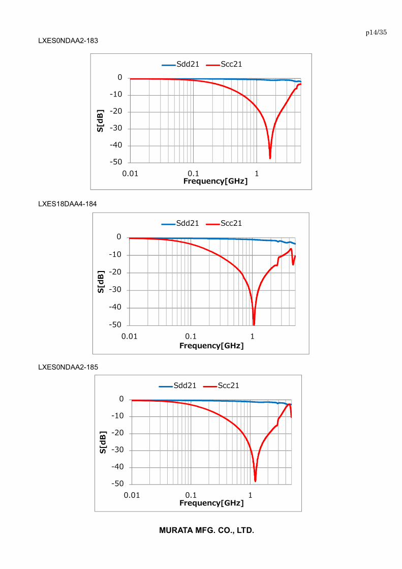
S parameter
LXES11DAA2-135
LXES21DAA4-136
LXES11DAA2-137
-50
-40
-30
-20
-10
0
0.01 0.1 1
S[dB]
Frequency[GHz]
Sdd21 Scc21
-50
-40
-30
-20
-10
0
0.01 0.1 1
S[dB]
Frequency[GHz]
Sdd21 Scc21
-50
-40
-30
-20
-10
0
0.01 0.1 1
S[dB]
Frequency[GHz]
Sdd21 Scc21

p12/35
MURATA MFG. CO., LTD.
LXES21DAA4-138
LXES21DAA4-140
LXES18DAA4-167
-50
-40
-30
-20
-10
0
0.01 0.1 1
S[dB]
Frequency[GHz]
Sdd21 Scc21
-50
-40
-30
-20
-10
0
0.01 0.1 1
S[dB]
Frequency[GHz]
Sdd21 Scc21
-50
-40
-30
-20
-10
0
0.01 0.1 1
S[dB]
Frequency[GHz]
Sdd21 Scc21

p13/35
MURATA MFG. CO., LTD.
LXES0NDAA2-172
LXES18DAA4-182
-50
-40
-30
-20
-10
0
0.01 0.1 1
S[dB]
Frequency[GHz]
Sdd21 Scc21
-50
-40
-30
-20
-10
0
0.01 0.1 1
S[dB]
Frequency[GHz]
Sdd21 Scc21
p14/35
MURATA MFG. CO., LTD.
LXES0NDAA2-183
LXES18DAA4-184
LXES0NDAA2-185
-50
-40
-30
-20
-10
0
0.01 0.1 1
S[dB]
Frequency[GHz]
Sdd21 Scc21
-50
-40
-30
-20
-10
0
0.01 0.1 1
S[dB]
Frequency[GHz]
Sdd21 Scc21
-50
-40
-30
-20
-10
0
0.01 0.1 1
S[dB]
Frequency[GHz]
Sdd21 Scc21

p15/35
MURATA MFG. CO., LTD.
Signal Integrity HDMI 1080P 48bit 0ohm w/t LXES11DAA2-135
Signal Integrity USB2.0 0ohm w/t LXES11DAA2-135
Signal Integrity USB3.0 0ohm w/t LXES11DAA2-135

p16/35
MURATA MFG. CO., LTD.
Signal Integrity HDMI 1080P 48bit 0ohm w/t LXES21DAA4-136
Signal Integrity USB2.0 0ohm w/t LXES21DAA4-136
Signal Integrity USB3.0 0ohm w/t LXES21DAA4-136
p17/35
MURATA MFG. CO., LTD.
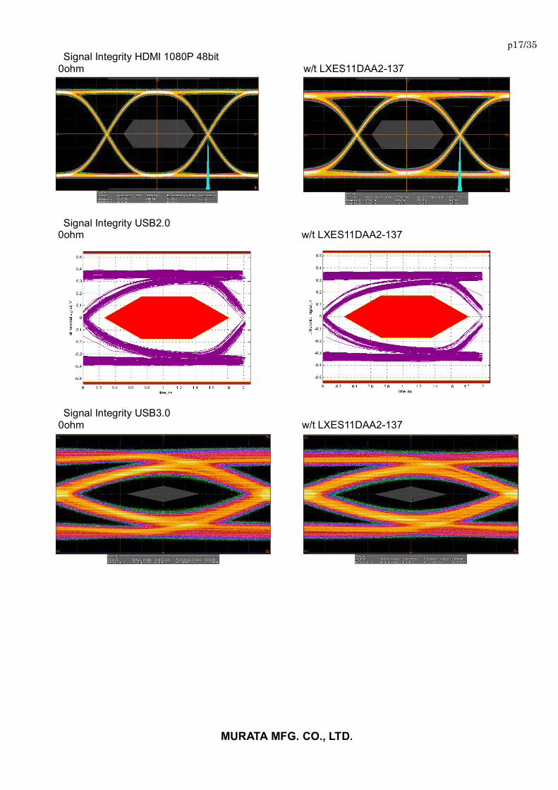
Signal Integrity HDMI 1080P 48bit 0ohm w/t LXES11DAA2-137
Signal Integrity USB2.0 0ohm w/t LXES11DAA2-137
Signal Integrity USB3.0 0ohm w/t LXES11DAA2-137

p18/35
MURATA MFG. CO., LTD.
Signal Integrity HDMI 1080P 48bit 0ohm w/t LXES21DAA4-138
Signal Integrity USB2.0 0ohm w/t LXES21DAA4-138
Signal Integrity USB3.0 0ohm w/t LXES21DAA4-138

p19/35
MURATA MFG. CO., LTD.
Signal Integrity HDMI 1080P 48bit 0ohm w/t LXES21DAA4-140
Signal Integrity USB2.0 0ohm w/t LXES21DAA4-140
Signal Integrity USB3.0 0ohm w/t LXES21DAA4-140

p20/35
MURATA MFG. CO., LTD.
5.Reliability Test
No. Items Specifications Test Methods Number Result(Fail)
1 Vibration Resistance
No severe damages
Satisfy dimension specifications
Solder specimens on the testing jig (glass fluorine boards) shown in appended Fig.1 by a Pb free solder. The soldering shall be done either by iron or reflow and be conducted with care so that the soldering is uniform and free of defect such as by heat shock.
Frequency : 10~2000 HzAcceleration : 196 m/s2Direction : X,Y,Z 3 axisPeriod : 2 h on each directionTotal 6 h.
22G(0)
2 Shock
Solder specimens on the testing jig (glass fluorine boards) shown in appended Fig.1 by a Pb free solder. The soldering shall be done either by iron or reflow and be conducted with care so that the soldering is uniform and free of defect such as by heat shock
Acceleration : 14,700 m/s2Period : 0.3 ms.Cycle : 3 times
22G(0)
3 Deflection
Solder specimens on the testing jig (glass epoxy boards) shown in appended Fig.2 by a Pb free solder. The soldering shall be done either by iron or reflow and be conducted with care so that the soldering is uniform and free of defect such as by heat shock.
No damage with 1.6mm deflection
22G(0)
4 Soldering strength(Push Strength) 5N Minimum
Solder specimens onto test jig shown below. Apply pushing force at 0.5mm/s until electrode pads are peeled off or ceramics are broken. Pushing force isapplied to longitudinal direction.
22G(0)
5 Solderability of Termination
95% of the terminations is to be soldered evenly and continuously.
Immerse specimens first an ethanol solution of rosin, then in a Pb free solder solution for 3±0.5 sec. at 245±5 °C.
Preheat : 10 0-120 °C, 60 sec.Solder Paste : Sn-3.0Ag-0.5CuFlux : Solution of ethanol and rosin (25 % rosin in weight proportion)
22G(0)
6
Resistance to Soldering Heat
(Reflow)
Appearance
Electrical specifications
No severe damages
Satisfy specifications listed in paragraph 4-2 over operational temperature range
Preheat Temperature : 150-200 °CPreheat Period : 120+/ -60 sHigh Temperature : 217℃
High Temp. Period : 105+/-45 sPeak Temperature : 260+0/ -5 °C
Specimens are soldered twice with the above condition, and then kept in room condition for 24 h before measurements.
22G(0)
Pushing Direction
JigSpecimen
p21/35
MURATA MFG. CO., LTD.
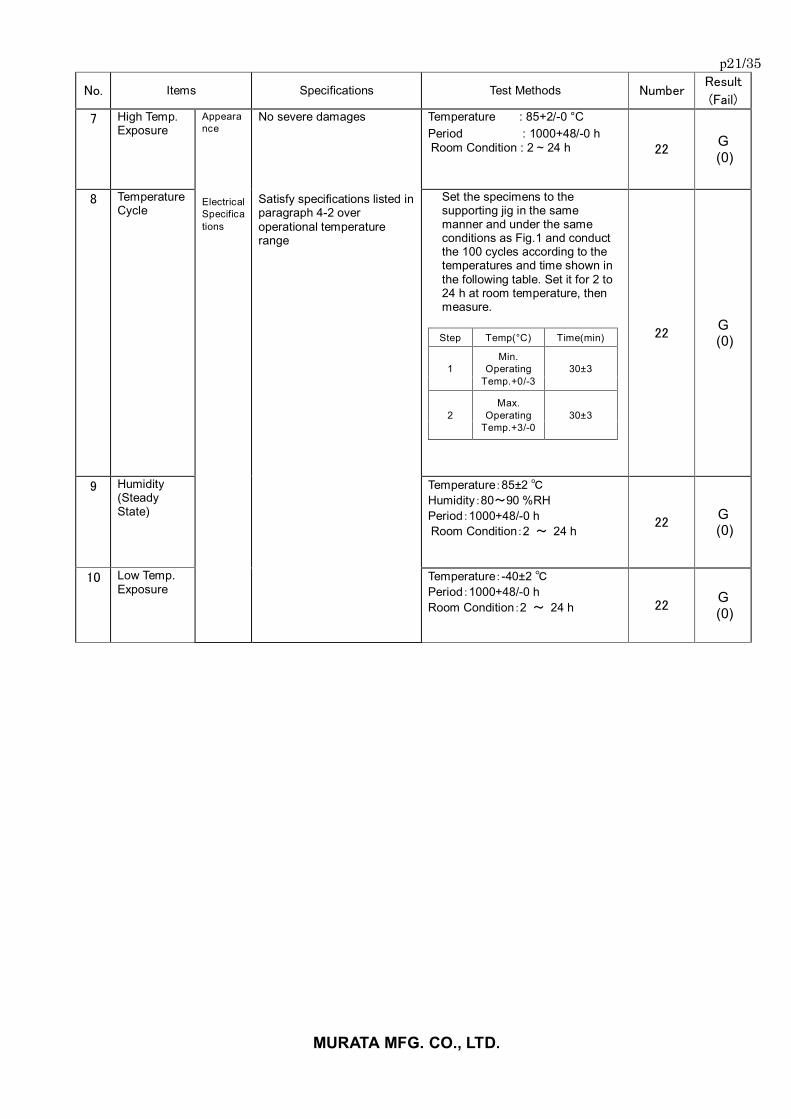
No. Items Specifications Test Methods NumberResult
(Fail)
7 High Temp.Exposure
Appearance
ElectricalSpecifications
No severe damages
Satisfy specifications listed in paragraph 4-2 over operational temperature range
Temperature : 85+2/-0 °CPeriod : 1000+48/-0 hRoom Condition : 2 ~ 24 h 22
G(0)
8 Temperature Cycle
Set the specimens to the supporting jig in the same manner and under the same conditions as Fig.1 and conduct the 100 cycles according to the temperatures and time shown in the following table. Set it for 2 to 24 h at room temperature, then measure.
Step Temp(°C) Time(min)
1Min.
OperatingTemp.+0/-3
30±3
2Max.
OperatingTemp.+3/-0
30±3
22G(0)
9 Humidity (Steady State)
Temperature:85±2 ℃Humidity:80~90 %RHPeriod:1000+48/-0 hRoom Condition:2 ~ 24 h
22G(0)
10 Low Temp.Exposure
Temperature:-40±2 ℃Period:1000+48/-0 hRoom Condition:2 ~ 24 h 22
G(0)

p22/35
MURATA MFG. CO., LTD.
Fig. 1Reference Land Pattern
LXES11D series
Unit : mmMark Dimension Mark Dimension
a 0.6 e 1.75b 1.4 f 0.3c 0.2 g 0.25d 0.75
Notes : this land layout is for reference purpose only.
LXES21D series
Unit : mmMark Dimension Mark Dimension
a 0.5 e 0.5b 1.5 f 0.25c 0.25 g 0.75d 0.25
Notes : this land layout is for reference purpose only.

p23/35
MURATA MFG. CO., LTD.
LXES0ND series
Unit : mm
Mark Dimension Mark Dimensiona 0.2 d 0.39b 0.4 e 0.095c 0.265 f 0.17
Notes: this land layout is for reference purpose only.
LXES18D series
Unit : mmMark Dimension Mark Dimension
a 0.35 e 0.47b 1.3 f 0.15c 0.2 g 0.48d 0.2
Notes : this land layout is for reference purpose only.

p24/35
MURATA MFG. CO., LTD.
Fig. 2Testing board
Unit : mm
Mounted situation
Test method
100
40
LandLand pattern is same as figure1Glass-fluorine board t=1.6mm
Copper thickness over 35 m
(Unit : mm)
(Unit : mm)
45 45
CHIP
R230
5020
deflection

p25/35
MURATA MFG. CO., LTD.
6.Tape and Reel Packing(1) LXES11D seriesDimensions of Tape
Unit : mm
(2) LXES21D seriesDimensions of Tape
Unit : mmMark Dimension Mark Dimension
L (2.25) c 4.00 +/-0.1W (1.45) d 3.50 +/-0.05T 1.1 max e 1.75 +/-0.10a 2.00 +/-0.05 f 8.00 +/-0.2b 4.00 +/-0.1 g φ1.55+/-0.05
Mark Dimension Mark DimensionL (1.40) c 4.00 +/-0.1W (1.20) d 3.50 +/-0.05T 1.03 max e 1.75 +/-0.10a 2.00 +/-0.05 f 8.00 +/-0.2b 4.00 +/-0.1 g φ1.55+/-0.05
f
e
d
c
b
aW
L
T
g

p26/35
MURATA MFG. CO., LTD.
(3) LXES0ND seriesDimensions of Tape
Unit : mmMark Dimension Mark Dimension
L (1.0) c 4.00 +/-0.1W (0.8) d 3.50 +/-0.05T 0.64 max e 1.75 +/-0.10a 2.00 +/-0.05 f 8.00 +/-0.10b 2.00 +/-0.1 g φ1.55+/-0.05
(4) LXES18D seriesDimensions of Tape
Unit : mmMark Dimension Mark Dimension
L (1.8) c 2.00 +/-0.05W (1.0) d 1.75 +/-0.1T 0.64 max e 3.50 +/-0.05a 4.00 +/-0.1 f 8.00 b 4.00 +/-0.1 g φ1.50
f
e
d
c
b
aW
L
T
g

p27/35
MURATA MFG. CO., LTD.
(3) Dimensions of Reel
Unit : mm
(4) Packaging
P/N pcs / reelLXES11D series 3,000LXES21D series 3,000LXES0ND series 10,000LXES18D series 4,000
Symbol a b c d e
Dimension 2.0 +/-0.5 φ13.0+/-0.2 9.0+1.0/-0 φ60+1.0/-0
φ180+0/-1.5
d e
cb
a

p28/35
MURATA MFG. CO., LTD.
(5) Taping Diagrams
[1] Feeding Hole : As specified in (1) (2)[2] Hole for chip : As specified in (1) (2)[3] Cover tape : 50 m in thickness[4] Base tape : As specified in (1) (2)
Marking Direction LXES11D series
LXES21D series
[1]
[2]
[3]
[3]
[4]
Feeding hole
Chip
Feedeng Direction
Feeding hole
Chip
Feedeng Direction

p29/35
MURATA MFG. CO., LTD.
LXES0ND series
LXES18D series
Chip
Feeding Direction
Feeding Hole

p30/35
MURATA MFG. CO., LTD.
(6) Leader and Tail tape
(7) The tape for chips are wound clockwise, the feeding holes to the right side as the tape is pulled toward the user.
(8) Material : Base tape ...... Plastic(LXES11D series/ LXES21D series) ...... Paper(LXES0ND series/ LXES18D series) Reel ...... Plastic Base tape, Reel and Top tape have an anti-ESD function.
(9) Peeling of force : 0.1~1.0 N in the direction of peeling as shown below.
165 to 180 °
0.1~1.0N
Cover tape
Tail tape(No components) Components No components
Feeding direction
Leader tape(Cover tape alone)
Over160mmOver100mm
Over400mm
Base tape

p31/35
MURATA MFG. CO., LTD.
NOTICE
1. Storage Conditions:
To avoid damaging the solderability of the external electrodes, be sure to observe the following points.
- Store products where the ambient temperature is 15 to 35 °C and humidity 45 to 75% RH.(Packing materials, In particular, may be deformed at the temperature over 40 °C.).
- Store products in non corrosive gas (Cl2, NH3,SO2, Nox, etc.).
- Stored products should be used within 6 months of receipt. Solderability should be verified if this period is exceeded.
This product is applicable to MSL1 (Based on IPC/JEDEC J-STD-020)
2. Handling Conditions:
Be careful in handling or transporting products because excessive stress or mechanical shock may break products due to the nature of ceramics structure.
Handle with care if products may have cracks or damages on their terminals, the characteristics of products may change. Do not touch products with bear hands that may result in poor solderability.
3. Standard PCB Design (Land Pattern and Dimensions):
All the ground terminals should be connected to the ground patterns. Furthermore, the ground pattern should be provided between IN and OUT terminals. Please refer to the specifications for the standard land dimensions.
The recommended land pattern and dimensions is as Murata's standard. The characteristics of products may vary depending on the pattern drawing method, grounding method, land dimensions, land forming method of the NC terminals and the PCB material and thickness. Therefore, be sure to verify the characteristics in the actual set. When using non-standard lands, contact Murata beforehand.
4. Notice for Chip Placer:
When placing products on the PCB, products may be stressed and broken by uneven forces from a worn-out chucking locating claw or a suction nozzle. To prevent products from damages, be sure to follow the specifications for the maintenance of the chip placer being used. For the positioning of products on the PCB, be aware that mechanical chucking may damage products.

p32/35
MURATA MFG. CO., LTD.
5. Soldering Conditions:
Carefully perform preheating so that the temperature difference (T) between the solder and products surface should be in the following range. When products are immersed in solvent after mounting, pay special attention to maintain the temperature difference within 100 °C. Soldering must be carried out by the above mentioned conditions to prevent products from damage. Contact Murata before use if concerning other soldering conditions.
Soldering method TemperatureSoldering iron method
<=130 °CReflow method
- Soldering iron method conditions are indicated below.
Kind of iron Item Ceramics heaterSoldering iron wattage <=18 WTemperature of iron-tip <=350 °CIron contact time within 3 sec
- Diameter of iron-tip : 3.0 mm max.- Do not allow the iron-tip to directly touch the ceramic element.
Use rosin type flux or weakly active flux with a chlorine content of 0.2 wt % or less.
Reflow soldering standard conditions(Example)
60-180 sec
Temperature (°C)
Pre-heating
Time (s.)
217 °C
60-150 sec.
Cooling down slowly
255-260 °C20-40 sec
MAX260 °C
150 °C
200 °C
255 °C

p33/35
MURATA MFG. CO., LTD.
Amount of Solder Paste:
- Ensure that solder is applied smoothly to a minimum height of 0.2 to 0.5 mm at the end surface of the external electrodes. If too much or little solder is applied, there is high possibility that the mechanical strength will be insufficient, creating the variation of characteristics.
Chassis
Lead wire of leaded component
Soldering iron
Solder resist
<Unacceptable>
<Improvements by land division >
High
Chip
Amount of solder paste
Chip
Chip
PCBLand
Solder (Grounding solder)
Solder resistSolder resist
Lead wire of component mounted later

p34/35
MURATA MFG. CO., LTD.
6. Cleaning Conditions:
Any cleaning is not permitted..
7. Operational Environment Conditions:
Products are designed to work for electronic products under normal environmental conditions (ambient temperature, humidity and pressure). Therefore, products have no problems to be used under the similar conditions to the above-mentioned. However, if products are used under the following circumstances, it may damage products and leakage of electricity and abnormal temperature may occur.
- In an atmosphere containing corrosive gas ( Cl2, NH3, SOx, NOx etc.).- In an atmosphere containing combustible and volatile gases.- In a dusty environment.- Direct sunlight- Water splashing place. - Humid place where water condenses. - In a freezing environment.
If there are possibilities for products to be used under the preceding clause, consult with Murata before actual use.
If product malfunctions may result in serious damage, including that to human life, sufficient fail-safe measures must be taken, including the following:(1) Installation of protection circuits or other protective device to improve system safety(2) Installation of redundant circuits in the case of single-circuit failure
8. Input Current and Voltage Capacity:
Products shall be used in the input current and voltage capacity as specified in this specification.Inform Murata beforehand, in case that the components are used beyond such input current and voltagecapacity range.
9. Limitation of Applications:
The products are designed and produced for application in ordinary electronic equipment(AV equipment, OA equipment, telecommunication, etc). If the products are to be used in devices requiring extremely high reliability following the application listed below, you should consult with the Murata staff in advance.
- Aircraft equipment.- Aerospace equipment- Undersea equipment.- Power plant control equipment.- Medical equipment.- Transportation equipment (vehicles, trains, ships, etc.).- Traffic signal equipment.- Disaster prevention / crime prevention equipment.- Data-procession equipment.- Application which malfunction or operational error may endanger human life and property of assets.- Application which related to occurrence the serious damage- Application of similar complexity and/ or reliability requirements to the applications listed in the above.

p35/35
MURATA MFG. CO., LTD.
! Note:Please make sure that your product has been evaluated and confirmed against your specifications when our product is mounted to your product.
Product specifications are subject to change or our products in it may be discontinued without advance notice.
This catalog is for reference only and not an official product specification document, therefore, please review and approve our official product specification before ordering this product.
Note:This catalog is for reference only and not an official product specifica tion document, therefore, please review and approve our official product specification before ordering this product.