Combined wet and dry cleaning of SiGe(001)kummelgroup.ucsd.edu/pubs/paper/Park_2015_JVSTA.pdf · TD...
8
Combined wet and dry cleaning of SiGe(001) Sang Wook Park, Tobin Kaufman-Osborn, and Hyonwoong Kim Materials Science and Engineering Program, University of California, San Diego, La Jolla, California 92093 Shariq Siddiqui and Bhagawan Sahu TD Research, GLOBALFOUNDRIES USA, Inc., 257 Fuller Road, Albany, New York 12203 Naomi Yoshida and Adam Brandt Applied Materials, Inc., Santa Clara, California 95054 Andrew C. Kummel a) Department of Chemistry and Biochemistry, University of California, San Diego, La Jolla, California 92093 (Received 31 December 2014; accepted 19 May 2015; published 17 June 2015) Combined wet and dry cleaning via hydrofluoric acid (HF) and atomic hydrogen on Si 0.6 Ge 0.4 (001) surface was studied at the atomic level using ultrahigh vacuum scanning tunneling microscopy (STM), scanning tunneling spectroscopy (STS), and x-ray photoelectron spectroscopy to under- stand the chemical transformations of the surface. Aqueous HF removes native oxide, but residual carbon and oxygen are still observed on Si 0.6 Ge 0.4 (001) due to hydrocarbon contamination from post HF exposure to ambient. The oxygen contamination can be eliminated by shielding the sample from ambient via covering the sample in the HF cleaning solution until the sample is introduced to the vacuum chamber or by transferring the sample in an inert environment; however, both processes still leave carbon contaminant. Dry in-situ atomic hydrogen cleaning above 330 C removes the carbon contamination on the surface consistent with a thermally activated atomic hydrogen reaction with surface hydrocarbon. A postdeposition anneal at 550 C induces formation of an atomically flat and ordered SiGe surface observed by STM. STS verifies that the wet and dry cleaned surface has an unpinned Fermi level with no states between the conduction and valence band edge comparable to sputter cleaned SiGe surfaces. V C 2015 American Vacuum Society. [http://dx.doi.org/10.1116/1.4922282] I. INTRODUCTION In order to overcome challenges when scaling down silicon-based complementary metal-oxide semiconductor devices, SiGe has received much attention due to its high car- rier mobility and application in strain engineering. 1–3 SiGe has a higher hole mobility, which makes it useful as a replace- ment for Si as a channel material in P-type metal-oxide-semi- conductor (PMOS) transistors. 4–6 Additionally, the larger lattice constant of SiGe can be utilized to improve electron mobility in N-type metal-oxide-semiconductor transistors by inducing a biaxial tensile strain into Si channels. 7–12 However, integration of SiGe as a channel material requires a clean and well-ordered surface for gate oxide deposition. 13 As the thickness of gate oxide scales down for high performance and low power consumption, a high quality interface between the high-k metal oxide and SiGe determines the device per- formance characteristics such as leakage current, mobility, and interface trap density (D it ). 14,15 Several cleaning procedures have been explored on SiGe surfaces. HCl solution cleaning is an ineffective method to remove native oxide because SiO 2 is inert to HCl solutions. 16 Hydrofluoric acid (HF) treatment removes all the surface oxides, leaving the surface hydrogen terminated after transfer to UHV as shown by synchrotron high resolution x-ray photo- electron spectroscopy (XPS); however, an inert processing environment is required to avoid oxygen and carbon contamination since the hydrogen passivated Si(001) and Ge(001) surfaces after HF cleaning are not stable in the ambi- ent air. 17–19 It is expected that GeH x species are less stable than SiH x species in ambient due to their weaker bonds. 19–21 Supercritical CO 2 containing HF and H 2 O removes all native oxides on SiGe surfaces; however, this method requires high HF concentrations resulting in rougher surfaces. 22 The study seeks to understand the chemical transforma- tions required to produce a clean and uniform SiGe(001) sur- face. A combined wet and dry cleaning procedure is employed to remove O and C, maximize the nucleation den- sity of high-k atomic layer deposition, and prepare a good template for subsequent forming gas anneal. 23–25 XPS meas- urements show that two newly developed HF wet clean methods remove the SiGe oxides leaving the surface chemi- cally passivated, thereby avoiding substrate oxidation even during ambient exposure. Even though ambient exposure results in hydrocarbon contamination, it is readily removed by subsequent atomic H exposure. The atomic H cleaning also induces Si segregation onto the surface while maintain- ing a good electronic structure. Si termination is likely to be advantageous for device performance due to the low defect density of Si/high-k dielectric interfaces after forming gas annealing. 26 Furthermore, Si termination on Ge PMOS tran- sistors minimizes the interface trap density (D it ). 27 In the present study, each experimental step is verified using in-situ XPS, scanning tunneling microscopy (STM), and scanning tunneling spectroscopy (STS). a) Electronic mail: [email protected] 041403-1 J. Vac. Sci. Technol. A 33(4), Jul/Aug 2015 0734-2101/2015/33(4)/041403/8/$30.00 V C 2015 American Vacuum Society 041403-1 Redistribution subject to AVS license or copyright; see http://scitation.aip.org/termsconditions. Download to IP: 68.101.209.36 On: Wed, 17 Jun 2015 13:54:23
Transcript of Combined wet and dry cleaning of SiGe(001)kummelgroup.ucsd.edu/pubs/paper/Park_2015_JVSTA.pdf · TD...
Combined wet and dry cleaning of SiGe(001)
Sang Wook Park, Tobin Kaufman-Osborn, and Hyonwoong KimMaterials Science and Engineering Program, University of California, San Diego, La Jolla, California 92093
Shariq Siddiqui and Bhagawan SahuTD Research, GLOBALFOUNDRIES USA, Inc., 257 Fuller Road, Albany, New York 12203
Naomi Yoshida and Adam BrandtApplied Materials, Inc., Santa Clara, California 95054
Andrew C. Kummela)
Department of Chemistry and Biochemistry, University of California, San Diego, La Jolla, California 92093
(Received 31 December 2014; accepted 19 May 2015; published 17 June 2015)
Combined wet and dry cleaning via hydrofluoric acid (HF) and atomic hydrogen on Si0.6Ge0.4(001)
surface was studied at the atomic level using ultrahigh vacuum scanning tunneling microscopy
(STM), scanning tunneling spectroscopy (STS), and x-ray photoelectron spectroscopy to under-
stand the chemical transformations of the surface. Aqueous HF removes native oxide, but residual
carbon and oxygen are still observed on Si0.6Ge0.4(001) due to hydrocarbon contamination from
post HF exposure to ambient. The oxygen contamination can be eliminated by shielding the sample
from ambient via covering the sample in the HF cleaning solution until the sample is introduced
to the vacuum chamber or by transferring the sample in an inert environment; however, both
processes still leave carbon contaminant. Dry in-situ atomic hydrogen cleaning above 330 �Cremoves the carbon contamination on the surface consistent with a thermally activated atomic
hydrogen reaction with surface hydrocarbon. A postdeposition anneal at 550 �C induces formation
of an atomically flat and ordered SiGe surface observed by STM. STS verifies that the wet and dry
cleaned surface has an unpinned Fermi level with no states between the conduction and valence
band edge comparable to sputter cleaned SiGe surfaces. VC 2015 American Vacuum Society.
[http://dx.doi.org/10.1116/1.4922282]
I. INTRODUCTION
In order to overcome challenges when scaling down
silicon-based complementary metal-oxide semiconductor
devices, SiGe has received much attention due to its high car-
rier mobility and application in strain engineering.1–3 SiGe
has a higher hole mobility, which makes it useful as a replace-
ment for Si as a channel material in P-type metal-oxide-semi-
conductor (PMOS) transistors.4–6 Additionally, the larger
lattice constant of SiGe can be utilized to improve electron
mobility in N-type metal-oxide-semiconductor transistors by
inducing a biaxial tensile strain into Si channels.7–12
However, integration of SiGe as a channel material requires a
clean and well-ordered surface for gate oxide deposition.13 As
the thickness of gate oxide scales down for high performance
and low power consumption, a high quality interface between
the high-k metal oxide and SiGe determines the device per-
formance characteristics such as leakage current, mobility,
and interface trap density (Dit).14,15
Several cleaning procedures have been explored on SiGe
surfaces. HCl solution cleaning is an ineffective method to
remove native oxide because SiO2 is inert to HCl solutions.16
Hydrofluoric acid (HF) treatment removes all the surface
oxides, leaving the surface hydrogen terminated after transfer
to UHV as shown by synchrotron high resolution x-ray photo-
electron spectroscopy (XPS); however, an inert processing
environment is required to avoid oxygen and carbon
contamination since the hydrogen passivated Si(001) and
Ge(001) surfaces after HF cleaning are not stable in the ambi-
ent air.17–19 It is expected that GeHx species are less stable
than SiHx species in ambient due to their weaker bonds.19–21
Supercritical CO2 containing HF and H2O removes all native
oxides on SiGe surfaces; however, this method requires high
HF concentrations resulting in rougher surfaces.22
The study seeks to understand the chemical transforma-
tions required to produce a clean and uniform SiGe(001) sur-
face. A combined wet and dry cleaning procedure is
employed to remove O and C, maximize the nucleation den-
sity of high-k atomic layer deposition, and prepare a good
template for subsequent forming gas anneal.23–25 XPS meas-
urements show that two newly developed HF wet clean
methods remove the SiGe oxides leaving the surface chemi-
cally passivated, thereby avoiding substrate oxidation even
during ambient exposure. Even though ambient exposure
results in hydrocarbon contamination, it is readily removed
by subsequent atomic H exposure. The atomic H cleaning
also induces Si segregation onto the surface while maintain-
ing a good electronic structure. Si termination is likely to be
advantageous for device performance due to the low defect
density of Si/high-k dielectric interfaces after forming gas
annealing.26 Furthermore, Si termination on Ge PMOS tran-
sistors minimizes the interface trap density (Dit).27 In the
present study, each experimental step is verified using in-situXPS, scanning tunneling microscopy (STM), and scanning
tunneling spectroscopy (STS).a)Electronic mail: [email protected]
041403-1 J. Vac. Sci. Technol. A 33(4), Jul/Aug 2015 0734-2101/2015/33(4)/041403/8/$30.00 VC 2015 American Vacuum Society 041403-1
Redistribution subject to AVS license or copyright; see http://scitation.aip.org/termsconditions. Download to IP: 68.101.209.36 On: Wed, 17 Jun 2015 13:54:23
II. EXPERIMENT
N-type Si0.6Ge0.4(001) layers with 4� 1019 cm�3 P
doping grown on Si(001) were prepared by Applied
Materials and diced into 12� 4.5 mm pieces. Samples
were degreased with acetone, methanol, and deionized
water using ultrasonication three times then dried with N2
gas.
Samples were dipped into 2% HF solution for 2 min to
remove native oxide and loaded within 5 min into a custom
Omicron UHV chamber with a base pressure of 2� 10�10.
Samples were annealed at 100, 200, and 500 �C via direct
heating. The sample temperatures were monitored by a py-
rometer and heated at a rate of 1 �C/s. Chemical, topological,
and electronic properties were verified via XPS, STM, and
STS in each experiment.
Two methods, “toluene double dip” and “HF drop,”
were investigated to eliminate residual oxygen on the
surface. It was hypothesized that residual oxygen on the
surface came from ambient hydrocarbon; therefore, deposi-
tion of a clean hydrocarbon capping layer was investigated.
For the toluene double dip method, toluene was layered
onto 2% HF solution to coat the SiGe upon removal from
the HF solution; to insure no residual HF, after the samples
were pulled out of the solution, samples were transferred to
another toluene solution. SiGe surfaces remained covered
with a layer of toluene to minimize air exposure during the
transfer. In HF drop, after the normal HF clean without
toluene, an additional 2% HF solution was dropped onto
samples in the load lock under N2 purge and evaporated in
the load lock chamber during pump down to a base pressure
of 2� 10�8 Torr. After each cleaning method, the samples
were annealed at 150 and 300 �C via resistive PBN heating;
the surface composition after each step was determined by
in-situ XPS.
After the drop clean method, SiGe samples were exposed
to atomic hydrogen in the UHV chamber using a thermal gas
cracker (Atomic Hydrogen Source, Veeco). The gas pressure
was controlled via a leak valve and measured through an ion
gauge; the exposure was calculated in terms of Langmuirs
[1 Langmuir (L)¼ 1� 10�6 Torr 1 s]. During the gas dosing,
the filament temperature of thermal gas cracker was
1800–2200 �C while SiGe(001) samples were maintained at
330 �C using a resistive PBN heater. The exposure pressures
were measured with an ion gauge and calculated in
Langmuirs; therefore, the reported doses are based on the H2
pressure and are an upper limit to the true exposure. The
cracking efficiency is expected to be 30% (Veeco), but it
could not be verified.
Samples were transferred to a STM chamber with a base
pressure of 1� 10�11 Torr. The atomic and electronic struc-
tures of SiGe surface in each experiment were studied with
in-situ STM and STS at 300 K (LT-STM, Omicron
Nanotechnology). Constant-current STM (Isp¼ 200 pA) was
operated with a sample bias between �1.8 and �2.0 V to
obtain filled state STM images. Variable-z mode STS was
operated using a modulation signal (0.1 V, 650 Hz) from
an external lock-in amplifier (SR830 DSP, Stanford
Research Systems) while sweeping the sample bias from
�1.5 to þ1.5 V.
Chemical analysis was performed using an in-situmonochromatic XPS (XM 1000 MkII/SPHERA, Omicron
Nanotechnology). Constant analyzer energy mode with a
pass energy of 50 eV and a line width of 0.1 eV using an Al
Ka source (1486.7 eV) were employed. The takeoff angle
was 30� from the sample surface, which is close to surface
parallel, and an acceptance angle of 67� was employed. For
peak shape analysis, CASA XPS v.2.3 was employed using a
Shirley background subtraction.
III. RESULTS AND DISCUSSION
A. Wet cleaning
Si0.6Ge0.4(001) surfaces were cleaned via a 2% HF
solution method leaving the surface hydrogen terminated
at room temperature as reported in a previous study using
synchrotron radiation photoelectron spectroscopy.16 Figure
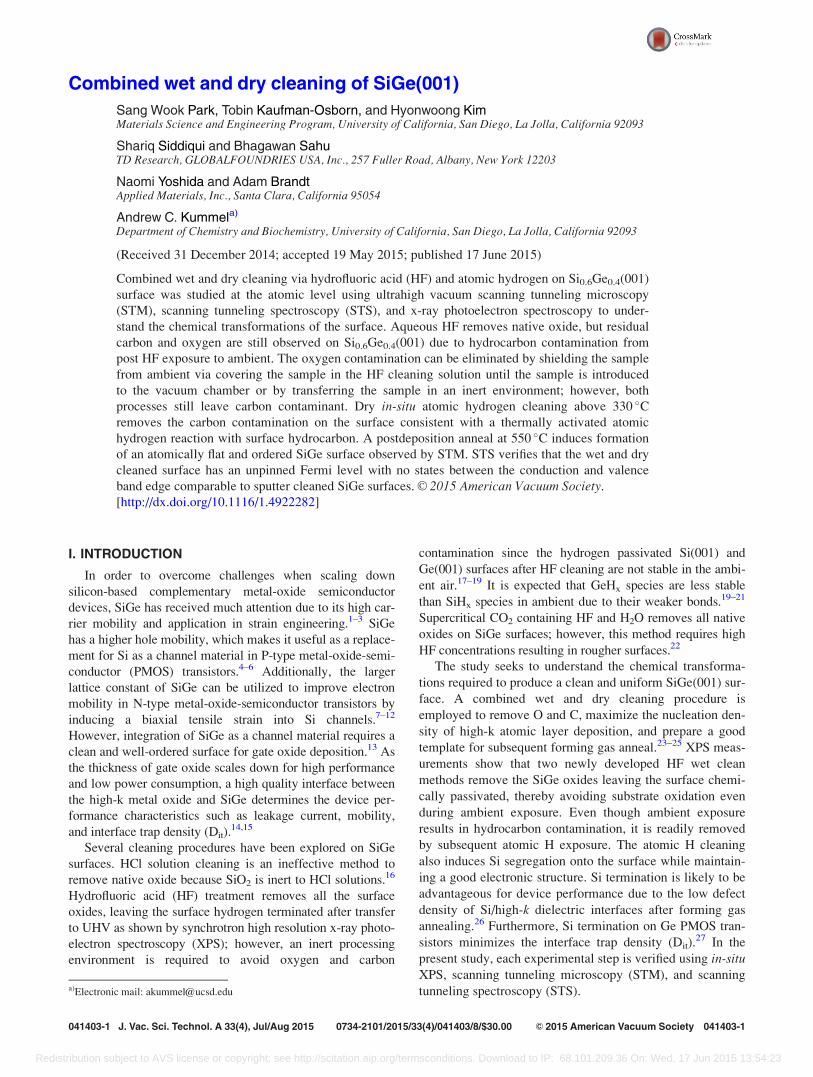
1(a) shows XPS results of SiGe(001) surface after 100,
200, and 500 �C anneals. All XPS peaks are normalized by
photoelectron cross-sections (Si2p-0.817, Ge 3d-1.42, O
1s-2.93, C 1s-1) using Hartree–Slater atomic model.28
Moreover, it is assumed that elements such as oxygen
and carbon are present as adsorbates on the SiGe(001)
substrate. Since the escape depth of electrons from the
Si2p and Ge3d peak is approximately 1 nm for a detection
angle of 30� from the sample surface based on a model by
Seah and Dench,29 for the 44% in the C/(SiþGe) and
14% in the O/(SiþGe) ratios shown in Fig. 1, the real
surface concentrations correspond to approximately 2.3
FIG. 1. (Color online) XPS and STM of wet cleaned SiGe(001). (a) XPS
data of HF wet cleaned SiGe(001) surface followed by annealing at 100,
200, and 500 �C. The ratio of each chemical element is normalized to the
sum of all components of Si 2p and Ge 3d peaks. (b) Filled state STM image
(50� 50 nm2, Vs¼�1.8 V, and It¼ 200 pA) of wet cleaned and 500 �Cannealed SiGe(001). (c) Line trace analysis of four different areas on STM
image (left). Vertical order is shown and average of row spacing is 1.2 nm
with a standard error of 0.055 nm.
041403-2 Park et al.: Combined wet and dry cleaning of SiGe(001) 041403-2
J. Vac. Sci. Technol. A, Vol. 33, No. 4, Jul/Aug 2015
Redistribution subject to AVS license or copyright; see http://scitation.aip.org/termsconditions. Download to IP: 68.101.209.36 On: Wed, 17 Jun 2015 13:54:23
ML carbon and 0.7 ML oxygen. These numerical values
are obtained based on a simplified model in which the top
three monolayers are purely composed of C and O atoms
and the lower layers are composed of Si and Ge atoms
and the attenuation is estimated using the formula
I¼ Ioexp(�t/k) (I: intensity in the presence of the over-
layer, Io: intensity in the absence of any covering layer, t:
thickness of the layer, k: inelastic mean free path). The
presence of oxygen is likely due to Si because Si-O bonds
are stronger than Ge-O bonds and because H terminated
Ge(001) exhibits only carbon contamination in ambient as
shown by Rivillon et al.19 Moreover, as shown by Hirose
et al., Si(001) rapidly absorbs a submonolayer of oxygen
in ambient due to defects and weakly bound hydrides con-
sistent with Si in SiGe(001) being responsible for oxygen
contamination.21 It is expected that the H termination is
desorbed for the 500 �C anneal as shown in previous
reports.16,30 In the absence of strong adsorbate bonding,
the surface of SiGe(001) is terminated by Ge atoms due to
the segregation of Ge to the surface as reported in the pre-
vious studies.31–33 Density functional theory calculations
theoretically verified that clean SiGe(001) surfaces are
thermodynamically more stable when composed of Ge
atoms compared to Si atoms.34 The wet cleaned surface of
SiGe(001) shows a high percentage of Ge atoms because
the native oxide of SiGe is mainly composed of SiO2, and
the SiO2 is removed by wet HF thereby exposing the accu-
mulation of Ge underneath the native oxide as reported in
the previous report.35 Since the Si/Ge ratio is identical on
all surfaces independent of annealing condition (Fig. 1), it
is concluded that the wet cleaned surfaces are largely Ge
enriched.
XPS data show that wet HF cleaned SiGe surfaces contain
residual oxygen and carbon. Since no SiOx nor GeOx compo-
nents are present, the XPS data are consistent with the C and
O being in the form of hydrocarbon due to air exposure dur-
ing the transfer into the load lock. The surface concentration
of carbon and oxygen decreases upon heating to 200 �C.
However, as the temperature is increased up to 500 �C, the O
is transferred to Si atoms forming surface SiOx before the
hydrocarbon completely desorbs while in UHV adsorbate-
free annealed SiGe(001), Ge is terminated.34 In the previous
study, it is reported that “reverse segregation” at the surface
is induced between Si and Ge by atomic hydrogen exposure
because the Si-H bond is much stronger than Ge-H
bond.36,37 A similar phenomenon of reverse segregation
should be expected on the SiGe(001) surface if there is a full
monolayer of oxygen because the Si-O bond is much stron-
ger than the Ge-O bond.
Figure 1(b) shows a filled-state STM image of a
SiGe(001) surface after a 500 �C anneal. The STM image
shows that HF wet clean and 500 �C anneal result in a
surface with a root mean square (RMS) roughness of
0.40 nm. Since the wet clean surface contains only small
domains and a high concentration of surface contami-
nants, a line trace analysis is needed to accurately deter-
mine the surface atomic space. To determine the vertical
row spacing of HF wet cleaned and annealed SiGe(001)
surface, line traces of four different areas are analyzed in
Fig. 1(c). Line trace analysis shows an average row spac-
ing of 1.2 nm with a standard error (SE) of 0.055 nm con-
sistent with the row spacing of the ideal SiGe(001)
surface.
B. Toluene double dip
In the present study, two methods of enhanced wet clean-
ing, toluene double dip and HF drop, were investigated to
eliminate residual oxygen on the SiGe(001) surface. Since
residual oxygen mainly results from the air exposure during
the sample transfer, each method was designed to protect the
surface against oxidation by oxy-hydrocarbons from air by
covering the surface with a hydrophobic toluene layer or
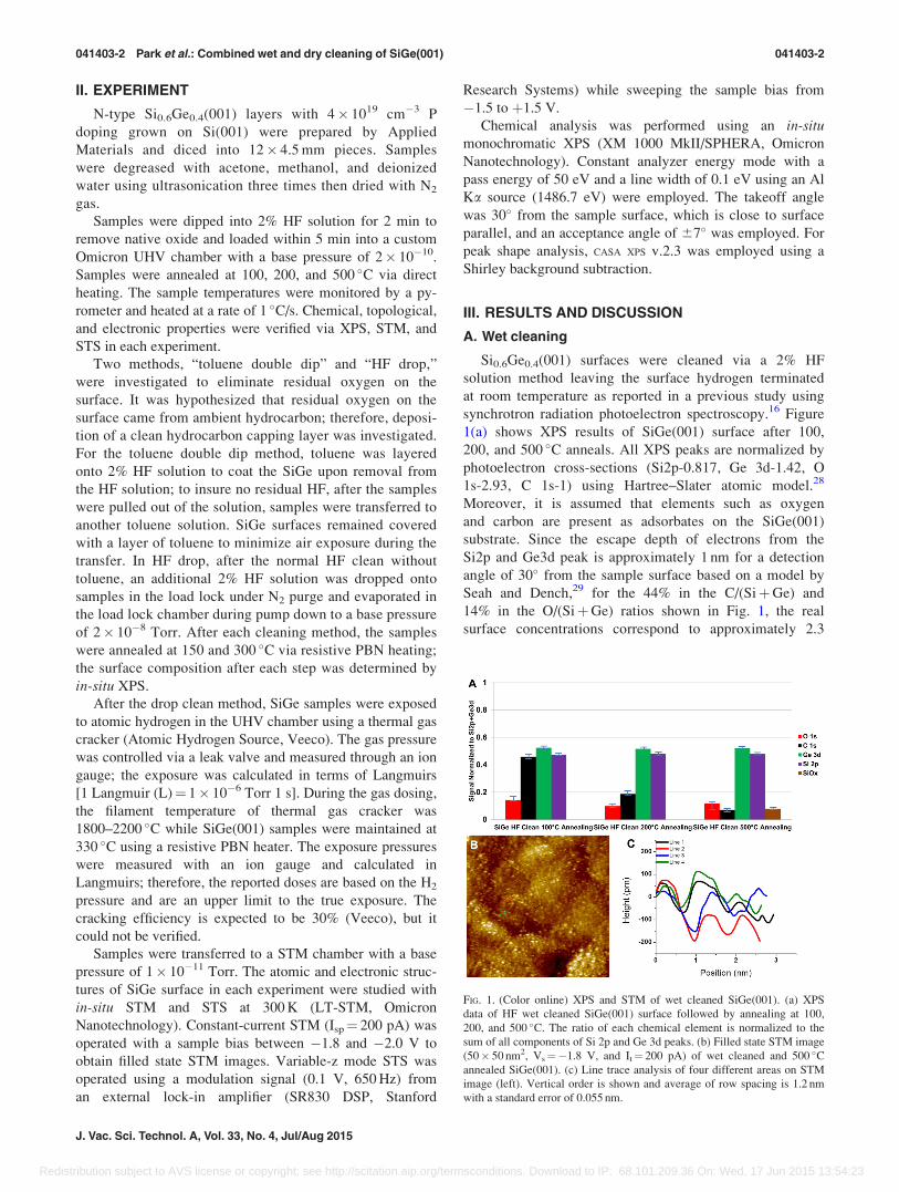
using an N2 purge. Figure 2(a) shows the schematic of the
toluene double dip method. It was hypothesized that if tolu-
ene sticks to the residual reactive sites on the HF wet cleaned
sample, this would inhibit adsorption of oxy-hydrocarbons.
Toluene is a hydrophobic molecule with strong internal
bonds, which should adsorb onto hydrogen terminated
SiGe(001) surface without any chemical reaction and easily
evaporate in a vacuum chamber due to its high vapor pres-
sure at RT. XPS data show that toluene double dip results in
no oxygen and low carbon contamination in Fig. 2(b). As the
sample temperature was increased to 300 �C, toluene capped
SiGe(001) surface had only 4% oxygen, which is 50%
smaller than normal HF cleaned SiGe(001). The residual
oxygen is probably due to contamination from the vacuum
system since it was not present on the sample prior to
annealing.
FIG. 2. (Color online) Schematic image and XPS of toluene double dip
method. (a) Schematic diagram of toluene double dip method. Wet HF
cleaned SiGe(001) samples are pulled through a layer of toluene then dipped
into another toluene solution. (b) XPS data of toluene double dip method
followed by 150 and 300 �C anneal.
041403-3 Park et al.: Combined wet and dry cleaning of SiGe(001) 041403-3
JVST A - Vacuum, Surfaces, and Films
Redistribution subject to AVS license or copyright; see http://scitation.aip.org/termsconditions. Download to IP: 68.101.209.36 On: Wed, 17 Jun 2015 13:54:23
C. Wet and dry cleaning
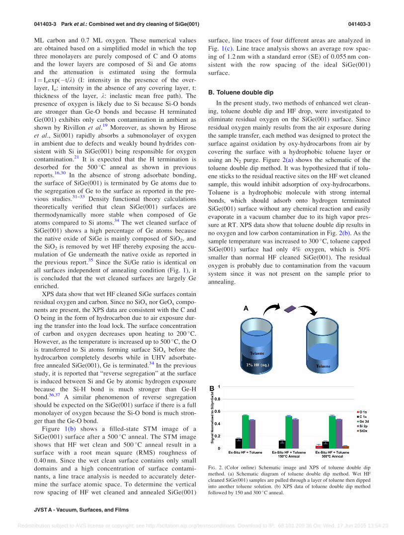
For the HF drop method, after HF wet clean, additional
HF solution is dropped onto SiGe(001) surface in the load
lock under N2 purge, which is known to stabilize Ge-H
bonds in ambient.19 The HF is evaporated in a vacuum
chamber during evacuation via a turbo pump. As shown in
Fig. 3(a), after the HF drop clean, the SiGe(001) surface
contains no oxygen, but still contains carbon comparable to
ex-situ HF clean.
To remove the carbon from the HF drop cleaned
SiGe(001) surface, atomic hydrogen was employed while
the substrate temperature was maintained at 330 �C. In the
previous studies, atomic hydrogen cleaning at temperatures
higher than 250 �C prevented preferential etching of Ge due
to inhibition of GeH2 formation at elevated temperature38,39
and atomic hydrogen cleaning is known to induce a Si segre-
gation on Ge-covered Si(001) by suppressing Ge segregation
above the substrate temperature of 250 �C.37 Additionally, it
was reported that atomic hydrogen suppresses the Ge surface
segregation during molecular beam epitaxy growth of Si/Ge
heterostructures.40 It is anticipated that similar phenomena
should be observed on SiGe(001) when dosed with atomic
hydrogen at 330 �C. The SiGe(001) surface was dosed with
18 000 L of atomic hydrogen while the substrate temperature
was maintained at 330 �C. XPS results in Fig. 3(a) show that
almost all carbon is eliminated, but 6% of oxygen is intro-
duced because the high temperature of tungsten filament of
thermal gas cracker induces wall desorption of oxygen in the
UHV chamber, which forms SiOx on Si-enriched SiGe(001)
surfaces. Figure 3(b) shows the spectrum of Ge 3d and Si 2p
peak after the wet HF drop method and dry atomic H clean.
Si 2p peak shows the formation of shoulder at higher binding
energy corresponding to SiOx after atomic H clean whereas
Ge 3d peak shows no changes. This is consistent with the
atomic H clean inducing or maintaining a Si enriched
SiGe(001) surface.
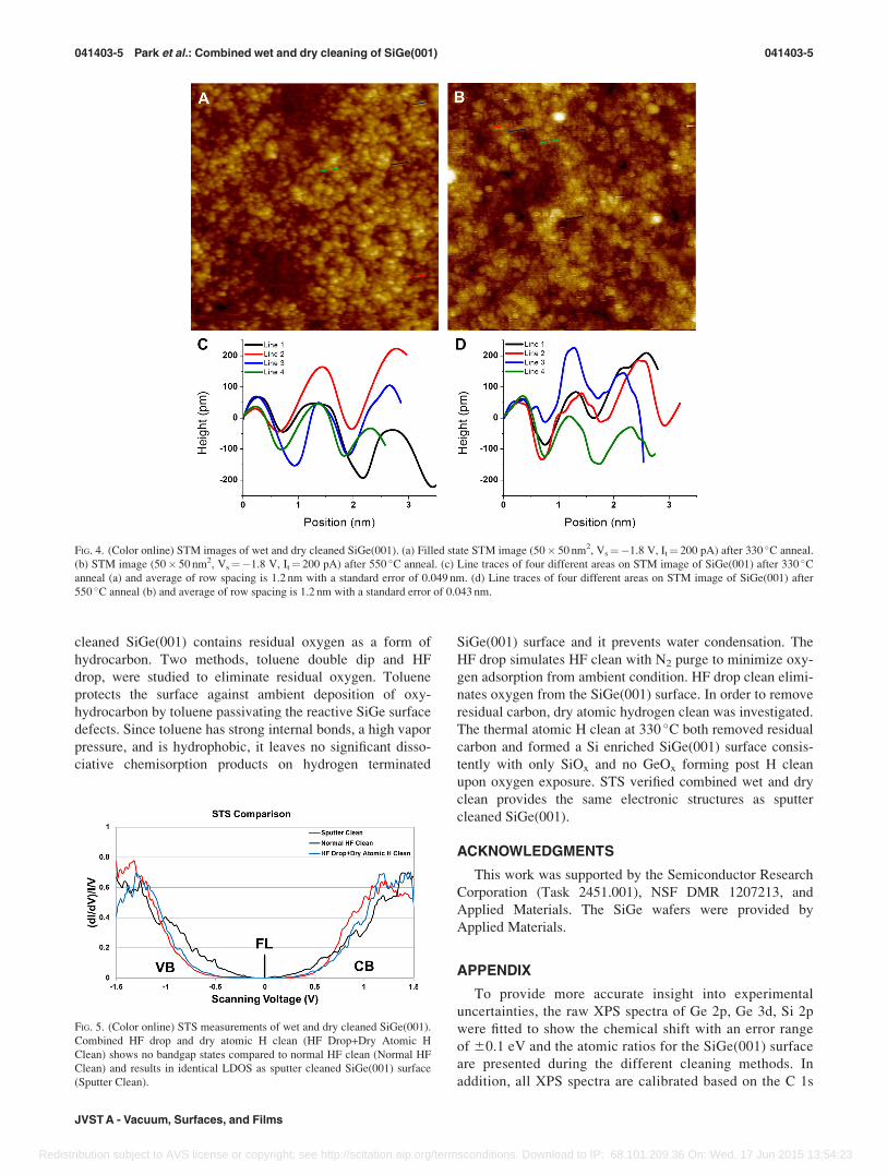
Figure 4 shows STM images of HF drop cleaned
SiGe(001) after atomic H cleaning at 330 �C and subse-
quent anneals at 330 and 550 �C. Due to the small domain
size and residual oxygen contamination, line trace analysis
is needed to quantitatively determine the surface order.
The SiGe(001) surfaces with only 330 �C anneal [Fig. 4(a)]
have a RMS roughness of 0.29 nm and an average row
spacing of 1.2 6 0.049 nm (SE) as shown in Fig. 4(c); this
is the identical row spacing as the sputter cleaned surface
and, therefore, consistent with the ideal row spacing of
SiGe(001) despite the small domain size and the residual
surface contamination. Post clean annealing at 550 �Cdecreases the RMS roughness from 0.29 to 0.23 nm while
maintaining 1.2 6 0.044 nm (SE) row spacing as shown in
Fig. 4(d); in addition, the STM images show no etch pits.
Compared to the HF wet cleaned surface, combined wet
and dry cleaning results in a flatter and more uniform sur-
face as shown by the 30% decrease in RMS roughness and
the appearance of distinct rows with the spacing of the
ideal sputter-cleaned surface. Lower RMS roughness and
the absence of etch pits are considered critical to high
channel mobility.41–44
STS measurements were taken to determine the effect of
the cleaning processes on the electronic structure of n-type
SiGe(001) surfaces. Pinning of Si0.6Ge0.4(001) results in a
Fermi level near the valence band similar to Ge(001) so STS
of n-type is sufficient to determine the unpinning of the sur-
face.45 STS measures the local density of states (LDOS) by
lock-in measurement of the AC signal from AC modulation
of the sample bias during an I-V (current–voltage) sweep
of the DC sample bias to obtain (dI/dV)/(I/V), which is con-
sidered to be proportional to the LDOS.46,47 STS curves in
Fig. 5 show the HF drop cleaned surface after both atomic H
cleaning and annealing at 550 �C produces an unpinned
surface with same electronic structure (HF DropþDry
Atomic H Clean) as sputter cleaned surface (Sputter Clean).
Moreover, no states are detected in the band gap region
between conduction and valence band edges in contrast to
normal HF cleaned surface with band gap states (Normal HF
Clean). This result demonstrates that a clean and unpinned
SiGe surface is obtained through combined wet HF and dry
atomic H cleaning method without sputter clean.
IV. SUMMARY AND CONCLUSIONS
HF wet clean was utilized to remove the native oxide of
Si0.6Ge0.4(001) surface; however, normal ex-situ HF wet
FIG. 3. (Color online) XPS analysis of wet plus dry cleaned SiGe(001). (a)
XPS data of HF drop method followed by 18 000 L atomic H clean shows
atomic H removes carbon from SiGe(001) surface. (b) XPS analysis before
and after atomic H clean show the change of spectrum in Ge 3d and Si 2p
peaks shows the absence of any initial Si and Ge oxides and only 6% SiOx
due to oxygen contamination during the atomic H clean.
041403-4 Park et al.: Combined wet and dry cleaning of SiGe(001) 041403-4
J. Vac. Sci. Technol. A, Vol. 33, No. 4, Jul/Aug 2015
Redistribution subject to AVS license or copyright; see http://scitation.aip.org/termsconditions. Download to IP: 68.101.209.36 On: Wed, 17 Jun 2015 13:54:23
cleaned SiGe(001) contains residual oxygen as a form of
hydrocarbon. Two methods, toluene double dip and HF
drop, were studied to eliminate residual oxygen. Toluene
protects the surface against ambient deposition of oxy-
hydrocarbon by toluene passivating the reactive SiGe surface
defects. Since toluene has strong internal bonds, a high vapor
pressure, and is hydrophobic, it leaves no significant disso-
ciative chemisorption products on hydrogen terminated
SiGe(001) surface and it prevents water condensation. The
HF drop simulates HF clean with N2 purge to minimize oxy-
gen adsorption from ambient condition. HF drop clean elimi-
nates oxygen from the SiGe(001) surface. In order to remove
residual carbon, dry atomic hydrogen clean was investigated.
The thermal atomic H clean at 330 �C both removed residual
carbon and formed a Si enriched SiGe(001) surface consis-
tently with only SiOx and no GeOx forming post H clean
upon oxygen exposure. STS verified combined wet and dry
clean provides the same electronic structures as sputter
cleaned SiGe(001).
ACKNOWLEDGMENTS
This work was supported by the Semiconductor Research
Corporation (Task 2451.001), NSF DMR 1207213, and
Applied Materials. The SiGe wafers were provided by
Applied Materials.
APPENDIX
To provide more accurate insight into experimental
uncertainties, the raw XPS spectra of Ge 2p, Ge 3d, Si 2p
were fitted to show the chemical shift with an error range
of 60.1 eV and the atomic ratios for the SiGe(001) surface
are presented during the different cleaning methods. In
addition, all XPS spectra are calibrated based on the C 1s
FIG. 4. (Color online) STM images of wet and dry cleaned SiGe(001). (a) Filled state STM image (50� 50 nm2, Vs¼�1.8 V, It¼ 200 pA) after 330 �C anneal.
(b) STM image (50� 50 nm2, Vs¼�1.8 V, It¼ 200 pA) after 550 �C anneal. (c) Line traces of four different areas on STM image of SiGe(001) after 330 �Canneal (a) and average of row spacing is 1.2 nm with a standard error of 0.049 nm. (d) Line traces of four different areas on STM image of SiGe(001) after
550 �C anneal (b) and average of row spacing is 1.2 nm with a standard error of 0.043 nm.
FIG. 5. (Color online) STS measurements of wet and dry cleaned SiGe(001).
Combined HF drop and dry atomic H clean (HF Drop+Dry Atomic H
Clean) shows no bandgap states compared to normal HF clean (Normal HF
Clean) and results in identical LDOS as sputter cleaned SiGe(001) surface
(Sputter Clean).
041403-5 Park et al.: Combined wet and dry cleaning of SiGe(001) 041403-5
JVST A - Vacuum, Surfaces, and Films
Redistribution subject to AVS license or copyright; see http://scitation.aip.org/termsconditions. Download to IP: 68.101.209.36 On: Wed, 17 Jun 2015 13:54:23
peak at 284.5 eV and the chemical shifts of the Ge 2p
peaks under all conditions are discussed due to its higher
surface sensitivity and accuracy resulting from small
escape depth and strong peak intensity compared to Ge 3d
and Si 2p peaks.
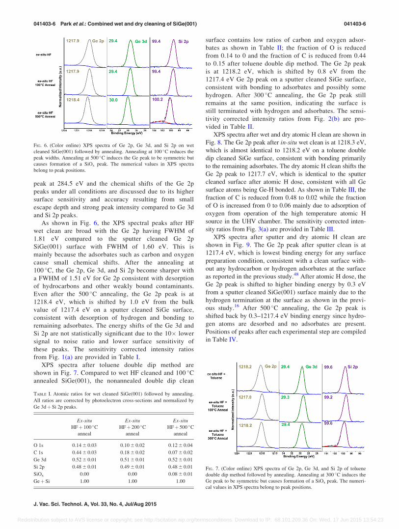
As shown in Fig. 6, the XPS spectral peaks after HF
wet clean are broad with the Ge 2p having FWHM of
1.81 eV compared to the sputter cleaned Ge 2p
SiGe(001) surface with FWHM of 1.60 eV. This is
mainly because the adsorbates such as carbon and oxygen
cause small chemical shifts. After the annealing at
100 �C, the Ge 2p, Ge 3d, and Si 2p become sharper with
a FWHM of 1.51 eV for Ge 2p consistent with desorption
of hydrocarbons and other weakly bound contaminants.
Even after the 500 �C annealing, the Ge 2p peak is at
1218.4 eV, which is shifted by 1.0 eV from the bulk
value of 1217.4 eV on a sputter cleaned SiGe surface,
consistent with desorption of hydrogen and bonding to
remaining adsorbates. The energy shifts of the Ge 3d and
Si 2p are not statistically significant due to the 10� lower
signal to noise ratio and lower surface sensitivity of
these peaks. The sensitivity corrected intensity ratios
from Fig. 1(a) are provided in Table I.
XPS spectra after toluene double dip method are
shown in Fig. 7. Compared to wet HF cleaned and 100 �Cannealed SiGe(001), the nonannealed double dip clean
surface contains low ratios of carbon and oxygen adsor-
bates as shown in Table II; the fraction of O is reduced
from 0.14 to 0 and the fraction of C is reduced from 0.44
to 0.15 after toluene double dip method. The Ge 2p peak
is at 1218.2 eV, which is shifted by 0.8 eV from the
1217.4 eV Ge 2p peak on a sputter cleaned SiGe surface,
consistent with bonding to adsorbates and possibly some
hydrogen. After 300 �C annealing, the Ge 2p peak still
remains at the same position, indicating the surface is
still terminated with hydrogen and adsorbates. The sensi-
tivity corrected intensity ratios from Fig. 2(b) are pro-
vided in Table II.
XPS spectra after wet and dry atomic H clean are shown in
Fig. 8. The Ge 2p peak after in-situ wet clean is at 1218.3 eV,
which is almost identical to 1218.2 eV on a toluene double
dip cleaned SiGe surface, consistent with bonding primarily
to the remaining adsorbates. The dry atomic H clean shifts the
Ge 2p peak to 1217.7 eV, which is identical to the sputter
cleaned surface after atomic H dose, consistent with all Ge
surface atoms being Ge-H bonded. As shown in Table III, the
fraction of C is reduced from 0.48 to 0.02 while the fraction
of O is increased from 0 to 0.06 mainly due to adsorption of
oxygen from operation of the high temperature atomic H
source in the UHV chamber. The sensitivity corrected inten-
sity ratios from Fig. 3(a) are provided in Table III.
XPS spectra after sputter and dry atomic H clean are
shown in Fig. 9. The Ge 2p peak after sputter clean is at
1217.4 eV, which is lowest binding energy for any surface
preparation condition, consistent with a clean surface with-
out any hydrocarbon or hydrogen adsorbates at the surface
as reported in the previous study.48 After atomic H dose, the
Ge 2p peak is shifted to higher binding energy by 0.3 eV
from a sputter cleaned SiGe(001) surface mainly due to the
hydrogen termination at the surface as shown in the previ-
ous study.16 After 500 �C annealing, the Ge 2p peak is
shifted back by 0.3–1217.4 eV binding energy since hydro-
gen atoms are desorbed and no adsorbates are present.
Positions of peaks after each experimental step are compiled
in Table IV.
FIG. 6. (Color online) XPS spectra of Ge 2p, Ge 3d, and Si 2p on wet
cleaned SiGe(001) followed by annealing. Annealing at 100 �C reduces the
peak widths. Annealing at 500 �C induces the Ge peak to be symmetric but
causes formation of a SiOx peak. The numerical values in XPS spectra
belong to peak positions.
TABLE I. Atomic ratios for wet cleaned SiGe(001) followed by annealing.
All ratios are corrected by photoelectron cross-sections and normalized by
Ge 3dþSi 2p peaks.
Ex-situHFþ 100 �C
anneal
Ex-situHFþ 200 �C
anneal
Ex-situHFþ 500 �C
anneal
O 1s 0.14 6 0.03 0.10 6 0.02 0.12 6 0.04
C 1s 0.44 6 0.03 0.18 6 0.02 0.07 6 0.02
Ge 3d 0.52 6 0.01 0.51 6 0.01 0.52 6 0.01
Si 2p 0.48 6 0.01 0.49 6 0.01 0.48 6 0.01
SiOx 0.00 0.00 0.08 6 0.01
GeþSi 1.00 1.00 1.00
FIG. 7. (Color online) XPS spectra of Ge 2p, Ge 3d, and Si 2p of toluene
double dip method followed by annealing. Annealing at 300 �C induces the
Ge peak to be symmetric but causes formation of a SiOx peak. The numeri-
cal values in XPS spectra belong to peak positions.
041403-6 Park et al.: Combined wet and dry cleaning of SiGe(001) 041403-6
J. Vac. Sci. Technol. A, Vol. 33, No. 4, Jul/Aug 2015
Redistribution subject to AVS license or copyright; see http://scitation.aip.org/termsconditions. Download to IP: 68.101.209.36 On: Wed, 17 Jun 2015 13:54:23
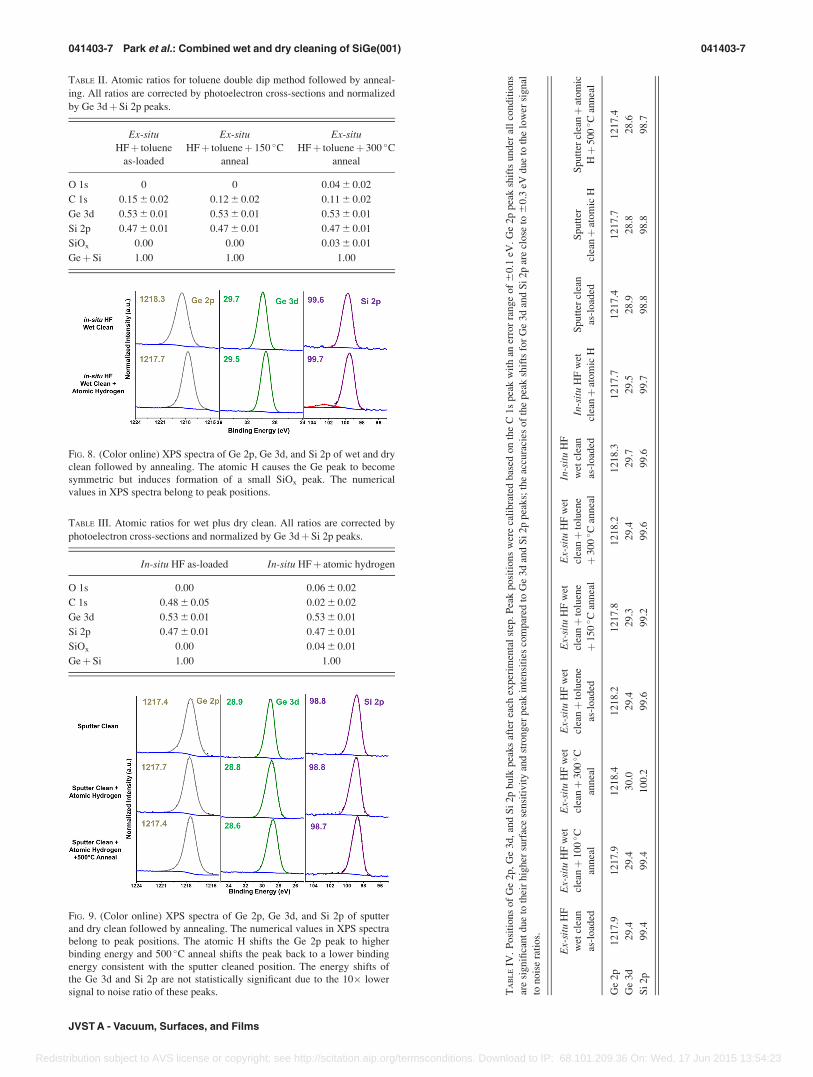
FIG. 9. (Color online) XPS spectra of Ge 2p, Ge 3d, and Si 2p of sputter
and dry clean followed by annealing. The numerical values in XPS spectra
belong to peak positions. The atomic H shifts the Ge 2p peak to higher
binding energy and 500 �C anneal shifts the peak back to a lower binding
energy consistent with the sputter cleaned position. The energy shifts of
the Ge 3d and Si 2p are not statistically significant due to the 10� lower
signal to noise ratio of these peaks. TA
BL
EIV
.P
osi
tions
of
Ge
2p,
Ge
3d,
and
Si
2p
bulk
pea
ks
afte
rea
chex
per
imen
tal
step
.P
eak
posi
tions
wer
eca
libra
ted
bas
edon
the
C1s
pea
kw
ith
aner
ror
range
of
60.1
eV.
Ge
2p
pea
ksh
ifts
under
all
condit
ions
are
signifi
cant
due
toth
eir
hig
her
surf
ace
sensi
tivit
yan
dst
ronger
pea
kin
tensi
ties
com
par
edto
Ge
3d
and
Si
2p
pea
ks;
the
accu
raci
esof
the
pea
ksh
ifts
for
Ge
3d
and
Si
2p
are
close
to6
0.3
eVdue
toth
elo
wer
signal
tonois
era
tios.
Ex-
situ
HF
wet
clea
n
as-l
oad
ed
Ex-
situ
HF
wet
clea
nþ
100� C
annea
l
Ex-
situ
HF
wet
clea
nþ
300� C
annea
l
Ex-
situ
HF
wet
clea
nþ
tolu
ene
as-l
oad
ed
Ex-
situ
HF
wet
clea
nþ
tolu
ene
þ150� C
annea
l
Ex-
situ
HF
wet
clea
nþ
tolu
ene
þ300� C
annea
l
In-s
itu
HF
wet
clea
n
as-l
oad
ed
In-s
itu
HF
wet
clea
nþ
atom
icH
Sputt
ercl
ean
as-l
oad
ed
Sputt
er
clea
nþ
atom
icH
Sputt
ercl
eanþ
atom
ic
Hþ
500� C
annea
l
Ge
2p
1217.9
1217.9
1218.4
1218.2
1217.8
1218.2
1218.3
1217.7
1217.4
1217.7
1217.4
Ge
3d
29.4
29.4
30.0
29.4
29.3
29.4
29.7
29.5
28.9
28.8
28.6
Si
2p
99.4
99.4
100.2
99.6
99.2
99.6
99.6
99.7
98.8
98.8
98.7
FIG. 8. (Color online) XPS spectra of Ge 2p, Ge 3d, and Si 2p of wet and dry
clean followed by annealing. The atomic H causes the Ge peak to become
symmetric but induces formation of a small SiOx peak. The numerical
values in XPS spectra belong to peak positions.
TABLE III. Atomic ratios for wet plus dry clean. All ratios are corrected by
photoelectron cross-sections and normalized by Ge 3dþSi 2p peaks.
In-situ HF as-loaded In-situ HFþ atomic hydrogen
O 1s 0.00 0.06 6 0.02
C 1s 0.48 6 0.05 0.02 6 0.02
Ge 3d 0.53 6 0.01 0.53 6 0.01
Si 2p 0.47 6 0.01 0.47 6 0.01
SiOx 0.00 0.04 6 0.01
GeþSi 1.00 1.00
TABLE II. Atomic ratios for toluene double dip method followed by anneal-
ing. All ratios are corrected by photoelectron cross-sections and normalized
by Ge 3dþSi 2p peaks.
Ex-situ
HFþ toluene
as-loaded
Ex-situ
HFþ tolueneþ 150 �Canneal
Ex-situ
HFþ tolueneþ 300 �Canneal
O 1s 0 0 0.04 6 0.02
C 1s 0.15 6 0.02 0.12 6 0.02 0.11 6 0.02
Ge 3d 0.53 6 0.01 0.53 6 0.01 0.53 6 0.01
Si 2p 0.47 6 0.01 0.47 6 0.01 0.47 6 0.01
SiOx 0.00 0.00 0.03 6 0.01
GeþSi 1.00 1.00 1.00
041403-7 Park et al.: Combined wet and dry cleaning of SiGe(001) 041403-7
JVST A - Vacuum, Surfaces, and Films
Redistribution subject to AVS license or copyright; see http://scitation.aip.org/termsconditions. Download to IP: 68.101.209.36 On: Wed, 17 Jun 2015 13:54:23

1F. Schaffler, Semicond. Sci. Technol. 12, 1515 (1997).2M. L. Lee, E. A. Fitzgerald, M. T. Bulsara, M. T. Currie, and A.
Lochtefeld, J. Appl. Phys. 97, 011101 (2005).3D. J. Paul, Semicond. Sci. Technol. 19, R75 (2004).4T. Mizuno, N. Sugiyama, H. Satake, and S. Takagi, Symp. VLSI Technol.,
Dig. Tech. Pap. 2000, 210.5T. Mizuno, S. Takagi, N. Sugiyama, H. Satake, A. Kurobe, and A.
Toriumi, IEEE Electron Device Lett. 21, 230 (2000).6M. L. Lee, C. W. Leitz, Z. Cheng, A. J. Pitera, T. Langdo, M. T. Currie,
G. Taraschi, E. A. Fitzgerald, and D. A. Antoniadis, Appl. Phys. Lett. 79,
3344 (2001).7S. Datta et al., Proceedings of the Bicmos Circuits and TechnologyMeeting (IEEE, 2004), pp. 194–197.
8S. Datta et al., IEEE Int. Electron Devices Meet., Tech. Dig. 2003, 653.9N. Griffin, D. D. Arnone, D. J. Paul, M. Pepper, D. J. Robbins, A. C.
Churchill, and J. M. Fernandez, J. Vac. Sci. Technol., B 16, 1655 (1998).10M. V. Fischetti, J. Appl. Phys. 89, 1232 (2001).11K. K. Rim, J. L. Hoyt, and J. F. Gibbons, IEEE Trans. Electron Devices
47, 1406 (2000).12S. H. Olsen, A. G. O’Neill, S. Chattopadhyay, L. S. Driscoll, K. S. K.
Kwa, D. J. Norris, A. G. Cullis, and D. J. Paul, IEEE Trans. Electron
Devices 51, 1245 (2004).13K. J. Kuhn, A. Murthy, R. Kotlyar, and M. Kuhn, ECS Trans. 33, 3 (2010).14K. Saraswat, C. O. Chui, T. Krishnamohan, D. Kim, A. Nayfeh, and A.
Pethe, Mater. Sci. Eng., B 135, 242 (2006).15Y. Taur and T. H. Ning, Fundamentals of Modern VLSI Devices, 2nd ed.
(Cambridge University, Cambridge; New York, 2009).16Y. Sun, Z. Liu, S. Y. Sun, and P. Pianetta, J. Vac. Sci. Technol., A 26,
1248 (2008).17Y. J. Chabal, G. S. Higashi, K. Raghavachari, and V. A. Burrows, J. Vac.
Sci. Technol., A 7, 2104 (1989).18X. Zhang, E. Garfunkel, Y. J. Chabal, S. B. Christman, and E. E. Chaban,
Appl. Phys. Lett. 79, 4051 (2001).19S. Rivillon, Y. J. Chabal, F. Amy, and A. Kahn, Appl. Phys. Lett. 87,
253101 (2005).20E. Yablonovitch, D. L. Allara, C. C. Chang, T. Gmitter, and T. B. Bright,
Phys. Rev. Lett. 57, 249 (1986).21F. Hirose, M. Nagato, Y. Kinoshita, S. Nagase, Y. Narita, and M.
Suemitsu, Surf. Sci. 601, 2302 (2007).22B. Xie, G. Montano-Miranda, C. C. Finstad, and A. J. Muscat, Mater. Sci.
Semicond. Process. 8, 231 (2005).23M. L. Reed and J. D. Plummer, J. Appl. Phys. 63, 5776 (1988).
24K. L. Brower, Appl. Phys. Lett. 53, 508 (1988).25K. L. Brower, Phys. Rev. B 38, 9657 (1988).26M. Caymax, F. Leys, J. Mitard, K. Martens, L. J. Yang, G. Pourtois, W.
Vandervorst, M. Meuris, and R. Loo, J. Electrochem. Soc. 156, H979
(2009).27M. Caymax, F. Leys, J. Mitard, K. Martens, L. J. Yang, G. Pourtois, W.
Vandervorst, M. Meuris, and R. Loo, ECS Transactions 19, 183 (2009).28J. H. Scofield, J. Electron Spectrosc. 8, 129 (1976).29M. P. Seah and W. A. Dench, Surf. Interface Anal. 1, 2 (1979).30P. Gupta, V. L. Colvin, and S. M. George, Phys. Rev. B 37, 8234 (1988).31D. J. Godbey and M. G. Ancona, J. Vac. Sci. Technol., B 11, 1392
(1993).32D. J. Godbey and M. G. Ancona, Appl. Phys. Lett. 61, 2217 (1992).33G. G. Jernigan, P. E. Thompson, and C. L. Silvestre, Surf. Sci. 380, 417
(1997).34T. Kaufman-Osborn, E. A. Chagarov, S. W. Park, B. Sahu, S. Siddiqui,
and A. C. Kummel, Surf. Sci. 630, 273 (2014).35H. K. Liou, P. Mei, U. Gennser, and E. S. Yang, Appl. Phys. Lett. 59,
1200 (1991).36Y. Kobayashi, K. Sumitomo, K. Shiraishi, T. Urisu, and T. Ogino, Surf.
Sci. 436, 9 (1999).37E. Rudkevich, F. Liu, D. E. Savage, T. F. Kuech, L. McCaughan, and M.
G. Lagally, Phys. Rev. Lett. 81, 3467 (1998).38Y. J. Zheng, P. F. Ma, and J. R. Engstrom, J. Appl. Phys. 90, 3614 (2001).39J. Y. Lee, S. J. Jung, J. Y. Maeng, Y. E. Cho, S. Kim, and S. K. Jo, Appl.
Phys. Lett. 84, 5028 (2004).40G. Ohta, S. Fukatsu, Y. Ebuchi, T. Hattori, N. Usami, and Y. Shiraki,
Appl. Phys. Lett. 65, 2975 (1994).41K. Sawano, K. Kawaguchi, T. Ueno, S. Koh, K. Nakagawa, and Y.
Shiraki, Mater. Sci. Eng., B 89, 406 (2002).42T. Yamanaka, S. J. Fang, H. C. Lin, J. P. Snyder, and C. R. Helms, IEEE
Electron Device Lett. 17, 178 (1996).43S. J. Fang, H. C. Lin, J. P. Snyder, C. R. Helms, and T. Yamanaka,
Electrochem. Soc. 96, 329 (1996).44T. Ohmi, K. Kotani, A. Teramoto, and M. Miyashita, IEEE Electron
Device Lett. 12, 652 (1991).45T. Kaufman-Osborn, E. A. Chagarov, and A. C. Kummel, J. Chem. Phys.
140, 204708 (2014).46R. M. Feenstra, Surf. Sci. 299–300, 965 (1994).47R. M. Feenstra, J. A. Stroscio, and A. P. Fein, Surf. Sci. 181, 295 (1987).48J. S. Hovis, R. J. Hamers, and C. M. Greenlief, Surf. Sci. 440, L815
(1999).
041403-8 Park et al.: Combined wet and dry cleaning of SiGe(001) 041403-8
J. Vac. Sci. Technol. A, Vol. 33, No. 4, Jul/Aug 2015
Redistribution subject to AVS license or copyright; see http://scitation.aip.org/termsconditions. Download to IP: 68.101.209.36 On: Wed, 17 Jun 2015 13:54:23