Combinational Logic Gates in CMOS - College of … · Combinational Logic Gates in CMOS ... np-CMOS...
49
Combinational Logic Gates in CMOS Prof. Kaushik Roy @ Purdue Univ. References: Adapted from: Digital Integrated Circuits: A Design Perspective, J. Rabaey © UCB Principles of CMOS VLSI Design: A Systems Perspective, 2nd Ed., N. H. E. Weste and K. Eshraghian EE216A Lecture Notes by Prof. K. Bult © UCLA
Transcript of Combinational Logic Gates in CMOS - College of … · Combinational Logic Gates in CMOS ... np-CMOS...
Combinational Logic Gates
in CMOS
Prof. Kaushik Roy
@ Purdue Univ.
References:
Adapted from: Digital Integrated Circuits: A Design Perspective, J. Rabaey © UCB
Principles of CMOS VLSI Design: A Systems Perspective, 2nd Ed.,
N. H. E. Weste and K. Eshraghian
EE216A Lecture Notes by Prof. K. Bult © UCLA

Improved Loads
Prof. Kaushik Roy
@ Purdue Univ.
Differential Cascade Voltage Switch Logic (DCVSL)
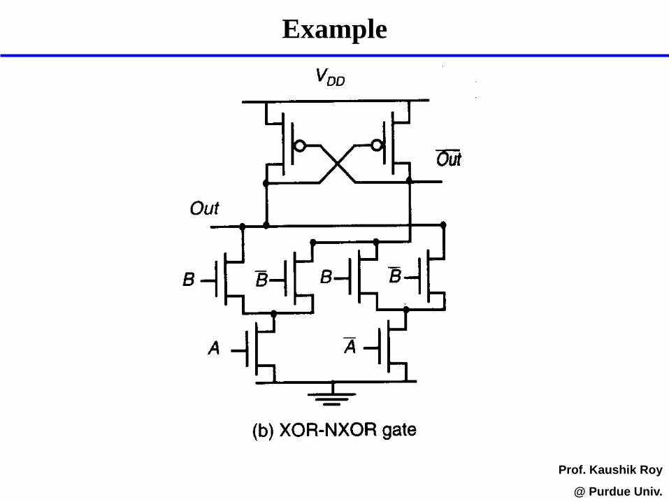
Example
Prof. Kaushik Roy
@ Purdue Univ.

Pass Transistor Logic
Prof. Kaushik Roy
@ Purdue Univ.

Pass-Transistor Logic
Prof. Kaushik Roy
@ Purdue Univ.
Switch
Network
A
B
B
B
• Reduced number of transistors
• No static power consumption

Pass Transistor Logic
Prof. Kaushik Roy
@ Purdue Univ.
F = Product Term
Control Signal
Pass
Signal
V
P
1 if
0 if
PV
P ZF
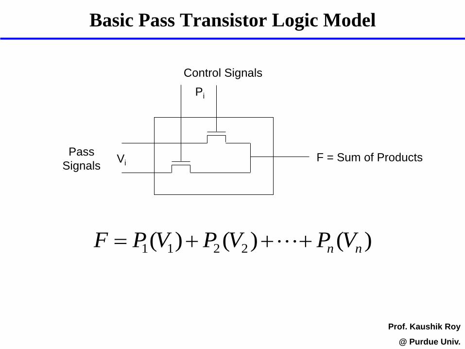
Basic Pass Transistor Logic Model
Prof. Kaushik Roy
@ Purdue Univ.
F = Sum of Products
Control Signals
Pass
Signals Vi
Pi
)()()( 2211 nn VPVPVPF

XNOR Gate
Prof. Kaushik Roy
@ Purdue Univ.
A
0
0
1
1
B
0
1
0
1
OUT
1
0
0
1
Pass Function
-A + -B
A + -B
-A + B
A + B
-A
A
-B
-B
Truth Table
B
Modified Karnaugh Map
0
1
-A
A
B
B
A
0 1
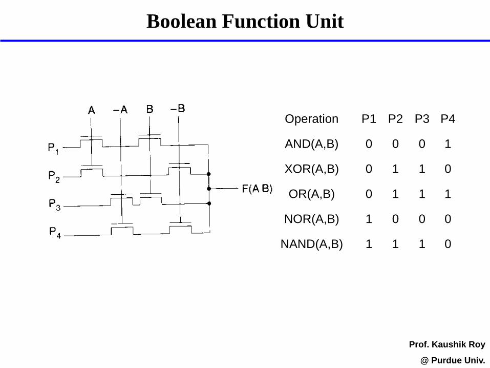
Boolean Function Unit
Prof. Kaushik Roy
@ Purdue Univ.
Operation
AND(A,B)
XOR(A,B)
OR(A,B)
NOR(A,B)
NAND(A,B)
P1
0
0
0
1
1
P2
0
1
1
0
1
P3
0
1
1
0
1
P4
1
0
1
0
0
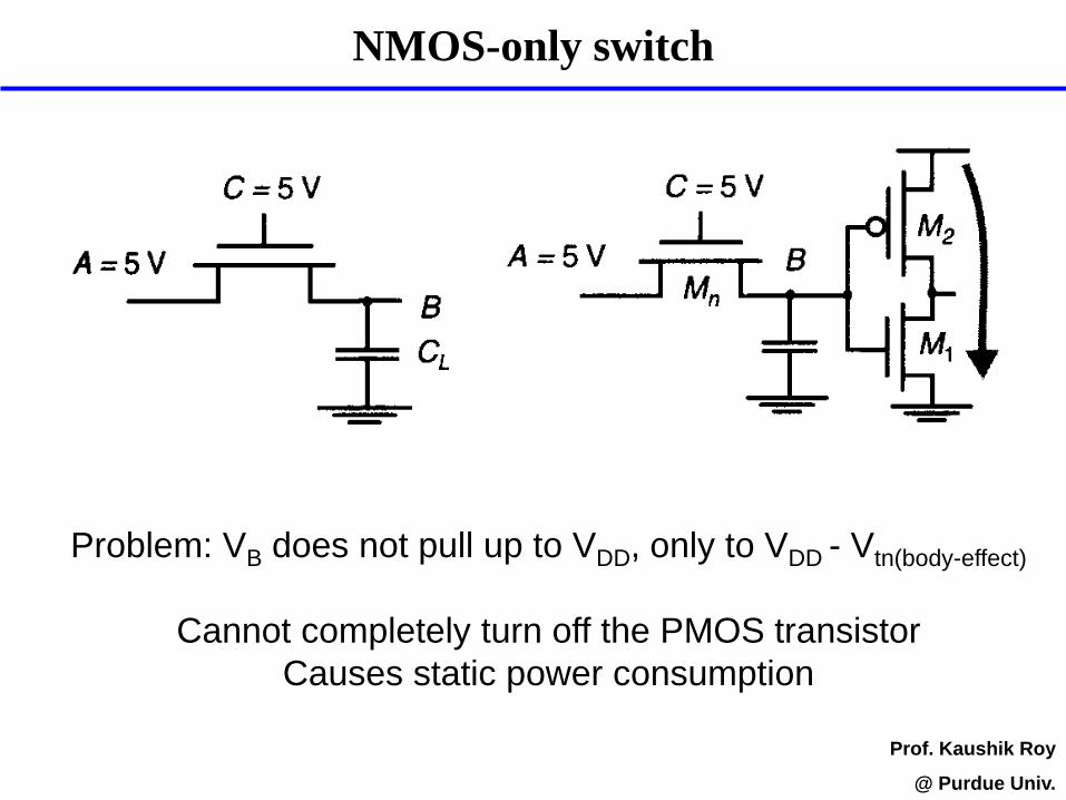
NMOS-only switch
Prof. Kaushik Roy
@ Purdue Univ.
Problem: VB does not pull up to VDD, only to VDD - Vtn(body-effect)
Cannot completely turn off the PMOS transistor
Causes static power consumption

Solution 1
Prof. Kaushik Roy
@ Purdue Univ.
Transmission Gate

Transmission Gate Implementation
Prof. Kaushik Roy
@ Purdue Univ.
P1
P2
P3
P4
-B B -A A
-B
B
F(A,B)
P1
P2
P3
P4
-B B -A A
F(A,B)
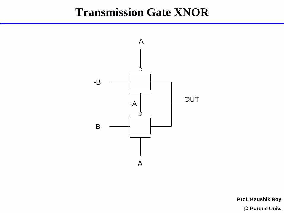
Transmission Gate XNOR
Prof. Kaushik Roy
@ Purdue Univ.
OUT
-B
B
-A
A
A
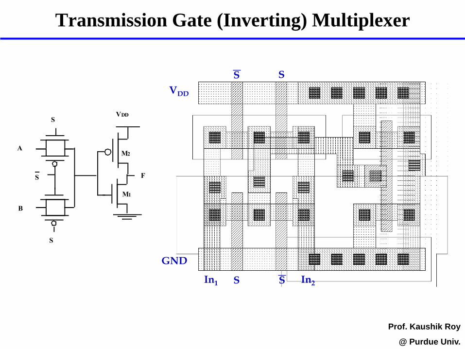
Transmission Gate (Inverting) Multiplexer
Prof. Kaushik Roy
@ Purdue Univ.
AM2
M1
B
S
S
S F
VDD
GND
VDD
In1 In2 S S
S S
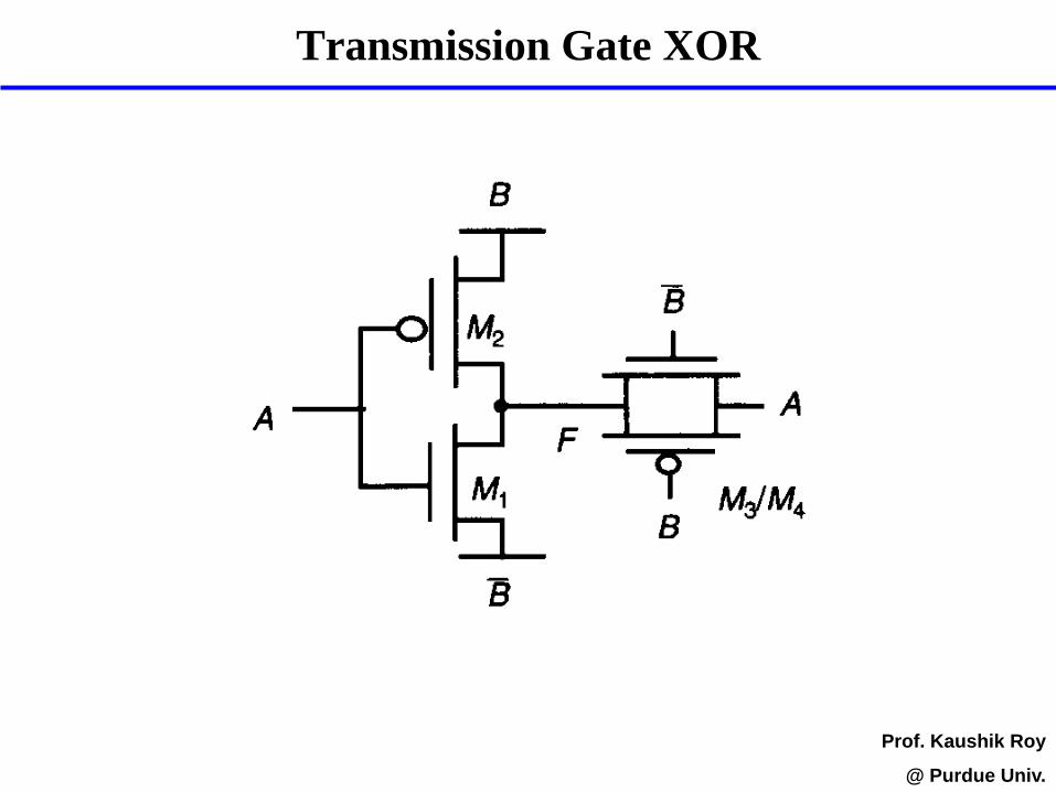
Transmission Gate XOR
Prof. Kaushik Roy
@ Purdue Univ.

Resistance of Transmission Gate
Prof. Kaushik Roy
@ Purdue Univ.
B is discharged originally
For NMOS, VGS = VDS, saturated or cutoff
For PMOS, VGS = -VDD, VDS increases from
-VDD to 0, starts out in saturation, then
transitions into non-saturation
:tpout VV
:tnDDouttp VVVV
:outtnDD VVV
NMOS saturated, PMOS saturated
NMOS saturated, PMOS linear
NMOS cutoff, PMOS linear

Resistance of Transmission Gate
Prof. Kaushik Roy
@ Purdue Univ.
Vout

Approximations
Prof. Kaushik Roy
@ Purdue Univ.
)()(
)(
))((
)(
))((
1
tpDDptnDDn
BA
BAtpDDp
BA
BAtnBDDn
eq
eq
VVVV
VV
VVVV
VV
VVVVV
RG
• Assume both in linear region, ignore body effect
• Assume both in saturated region
DD
tpDDptnDDn
DD
pn
eq
V
VVVV
V
IIG
2
)()( 22

When Output Closely follows Input
Prof. Kaushik Roy
@ Purdue Univ.
Ron
Vin
nmost pmost
Transmission gate
Region A:
NMOS unsaturated, PMOS off
Region B:
NMOS unsaturated, PMOS unsaturated
Region C:
NMOS off, PMOS unsaturated

Delay in Transmission Gate Networks
Prof. Kaushik Roy
@ Purdue Univ.
Distributed RC network

Elmore Delay
Prof. Kaushik Roy
@ Purdue Univ.
Estimate the dominant time constant:
assume all internal nodes are pre-charged to VDD,
and a step input is applied
)(2)()(1)(
11 tVtVtVCRdt
tdViii
eq
i
CRnn
CRRC eq
N
k
N
kj
N
k
N
kj
eqeqN2
)1(
1 1
To solve for actual delay

Delay Optimization by Buffer Insertion
Prof. Kaushik Roy
@ Purdue Univ.
• Delay of RC chain
• Delay of buffered chain
CRnn
t eqNp2
)1(69.069.0
CR
tm
tm
nCR
mn
tm
nCR
mm
m
nt
eq
pbuf
opt
pbufeq
pbufeqp
7.1
12
)1(69.0
12
)1(69.0

Transmission Gate Full Adder
Prof. Kaushik Roy
@ Purdue Univ.
A
B
P
Ci
VDDA
A A
VDD
Ci
A
P
AB
VDD
VDD
Ci
Ci
Co
S
Ci
P
P
P
P
P
Sum Generation
Carry Generation
Setup

Adder Truth Table
Prof. Kaushik Roy
@ Purdue Univ.
C
0
0
0
0
1
1
1
1
A
0
0
1
1
0
0
1
1
B
0
1
0
1
0
1
0
1
A.B(G)
0
0
0
1
0
0
0
1
A+B
0
1
1
1
0
1
1
1
A + B(P)
0
1
1
0
0
1
1
0
SUM
0
1
1
0
1
0
0
1
CARRY
0
0
0
1
0
1
1
1
SUM = A + B + C
CARRY = C if A + B = 1
CARRY = A (or B) if A + B = 0

Solution 2
Prof. Kaushik Roy
@ Purdue Univ.
Level Restoring Transistor for NMOS Only Logic
• Full Swing
• Disadvantage: More complex, larger capacitance

Proper Sizing of Level Restoring Transistor
Prof. Kaushik Roy
@ Purdue Univ.
• In transient, conducting path from Mr to M3 via Mn
when A is low, B switches from low to high, and X is
high
• Mr must not be too large, otherwise, X cannot be
brought below threshold voltage, VM, of inverter, Mr
cannot be turned off

Pass-Transistors
Prof. Kaushik Roy
@ Purdue Univ.
Single Transistor Pass Gate with VT=0
Out
VDD
VDD
5V
VDD
0V 5V
0V
WATCH OUT FOR LEAKAGE CURRENTS
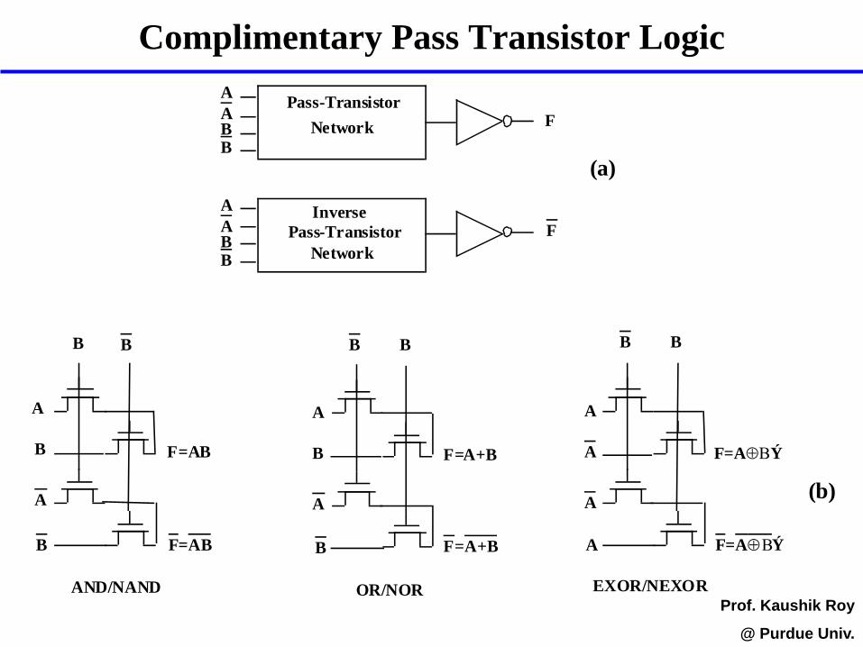
Complimentary Pass Transistor Logic
Prof. Kaushik Roy
@ Purdue Univ.
A
B
A
B
B B B B
A
B
A
B
F=AB
F=AB
F=A+B
F=A+B
B B
A
A
A
A
F=AÝ
F=AÝ
OR/NOR EXOR/NEXORAND/NAND
F
F
Pass-Transistor
Network
Pass-Transistor
Network
A
ABB
A
ABB
Inverse
(a)
(b)
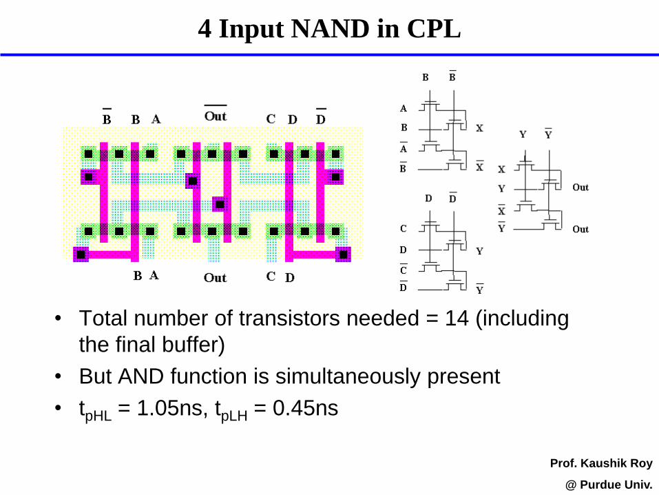
4 Input NAND in CPL
Prof. Kaushik Roy
@ Purdue Univ.
• Total number of transistors needed = 14 (including
the final buffer)
• But AND function is simultaneously present
• tpHL = 1.05ns, tpLH = 0.45ns

Dynamic Logic
Prof. Kaushik Roy
@ Purdue Univ.

Dynamic Logic
Prof. Kaushik Roy
@ Purdue Univ.
Mp
Me
VDD
PDN
In1
In2
In3
Out
Me
Mp
VDD
PUN
In1
In2
In3
Out
CL
CL
p networkn network
2 phase operation:• Evaluation
• Precharge
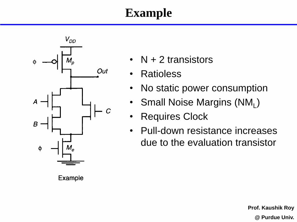
Example
Prof. Kaushik Roy
@ Purdue Univ.
• N + 2 transistors
• Ratioless
• No static power consumption
• Small Noise Margins (NML)
• Requires Clock
• Pull-down resistance increases
due to the evaluation transistor

Transient Response
Prof. Kaushik Roy
@ Purdue Univ.
0.00e+00 2.00e-09 4.00e-09 6.00e-09t (nsec)
0.0
2.0
4.0
6.0
Vout (V
olt)
Vout
PRECHARGEEVALUATION
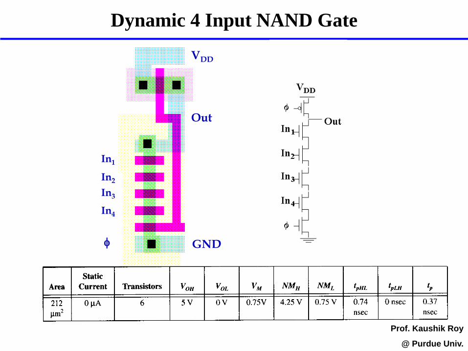
Dynamic 4 Input NAND Gate
In1
In2
In3
In4
Out
VDD
GND
Prof. Kaushik Roy
@ Purdue Univ.

Reliability Problems — Charge Leakage
Prof. Kaushik Roy
@ Purdue Univ.
Mp
Me
VDD
Out
A
CL(1)
(2)
t
t
Vout
(b) Effect on waveforms(a) Leakage sources
precharge evaluate
Minimum Clock Frequency: > 1 MHzDynamic circuits require a minimal clock rate

Charge Sharing (redistribution)
Prof. Kaushik Roy
@ Purdue Univ.
Mp
Me
VDD
Out
A
B = 0
CL
Ca
Cb
Ma
Mb
X
CL
VDD
CL
Vout
t Ca
VDD
VTn
VX – +=
or
Vout Vout t VDD–Ca
CL
-------- VDD VTn VX – –= =
Vout VDD
Ca
Ca
CL
+----------------------
–=
case 1) if Vout < VTn
case 2) if Vout > VTn

Minimize Charge Sharing
Prof. Kaushik Roy
@ Purdue Univ.
• Keep the change in storage voltage below | Vtp |
– the output might be connected to a static inverter as in
Domino logic
• Ca is normally smaller than CL, but if there is series
connection of NMOS transistors, internal
capacitances can be strung together and that can
increase the voltage change
2.0
tnDD
tp
L
a
VV
V
C
C

Charge Redistribution - Solutions
Prof. Kaushik Roy
@ Purdue Univ.
Mp
Me
VDD
Out
A
B
Ma
Mb
Mbl Mp
Me
VDD
Out
A
B
Ma
Mb
Mbl
(b) Precharge of internal nodes
(a) Static bleeder

Clock Feedthrough
Prof. Kaushik Roy
@ Purdue Univ.
Mp
Me
VDD
Out
A
B
CL
Ca
Cb
Ma
Mb
X
5V
overshoot
out
could potentially forwardbias the diode
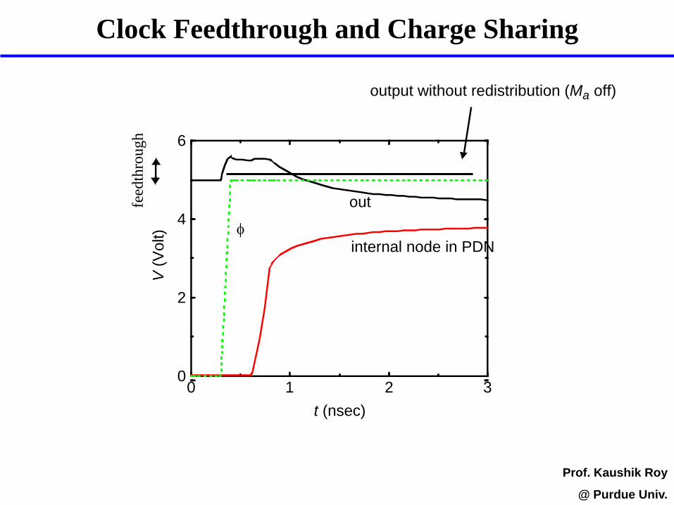
Clock Feedthrough and Charge Sharing
Prof. Kaushik Roy
@ Purdue Univ.
0 1 2 3
t (nsec)
0
2
4
6V
(V
olt)
out
internal node in PDN
output without redistribution (Ma off)
feed
thro
ug
h
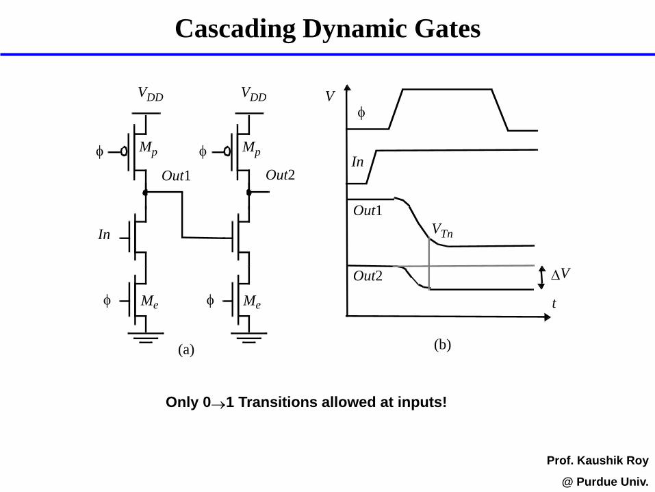
Cascading Dynamic Gates
Prof. Kaushik Roy
@ Purdue Univ.
Mp
Me
VDD
Mp
Me
VDD
In
Out1 Out2
Out2
Out1
In
V
t
V
VTn
(a) (b)
Only 01 Transitions allowed at inputs!

Domino Logic
Prof. Kaushik Roy
@ Purdue Univ.
Mp
Me
VDD
PDN
In1
In2
In3
Out1
Mp
Me
VDD
PDN
In4
Out2
Mr
VDD
Static Inverter
with Level Restorer

Domino Logic - Characteristics
Prof. Kaushik Roy
@ Purdue Univ.
• Only non-inverting logic
• Very fast - Only 10 transitions at input of inverter
affects the next Domino
• Static inverter increases noise immunity, increase the
size of PMOS to increase VM
• Proper sizing of inverter to drive the fan-out in optimal
way
• Add a level-restoring transistor to overcome charge
sharing and charge loss

np-CMOS (Zipper CMOS)
Prof. Kaushik Roy
@ Purdue Univ.
Mp
Me
VDD
PDN
In1In2
In3
Me
Mp
VDD
PUN
In4
Out1
Out2
Only 10 transitions allowed at inputs of PUN
Reduced noise margins: NMH = | Vtp |, NML = | Vtn |
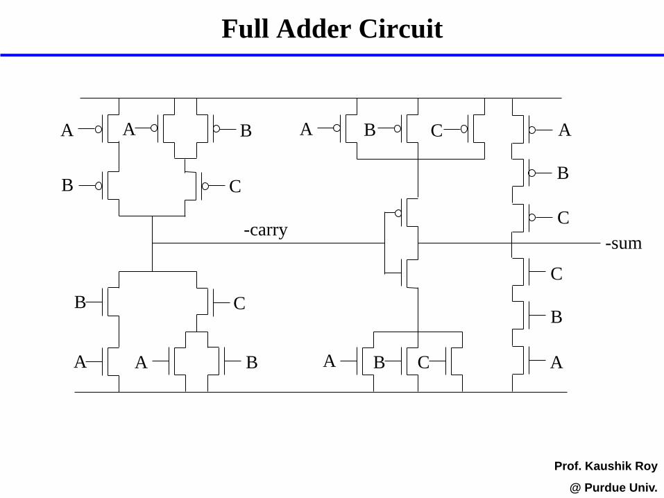
Full Adder Circuit
Prof. Kaushik Roy
@ Purdue Univ.
A
B
B
C
A
B
C B
A A
A B C A
A B C
B
C
C
B
A
-sum -carry
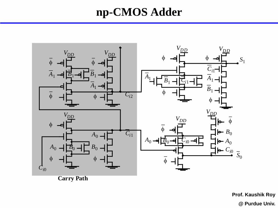
np-CMOS Adder
Prof. Kaushik Roy
@ Purdue Univ.
VDD
Ci0
A0 B0 B0
A0
VDD
B1
A1
VDD
A1 B1
Ci1
Ci2
Ci0
Ci0
B0
A0B0
S0
A0
VDD
VDD
VDD
B1 Ci1
B1
A1A1
VDD
S1
Ci1
Carry Path

Manchester Carry Chain Adder
Prof. Kaushik Roy
@ Purdue Univ.
P0
Ci,0
P1
G0
P2
G1
P3
G2
P4
G3 G4
VDD
M0 M1 M2 M3 M4
Co,4
11.522.53
3.5 3 2.5 2 1.5 1
1.522.533.54
0.5
Total Area:
225 m 48.6 m

Adder Truth Table
Prof. Kaushik Roy
@ Purdue Univ.
C
0
0
0
0
1
1
1
1
A
0
0
1
1
0
0
1
1
B
0
1
0
1
0
1
0
1
A.B(G)
0
0
0
1
0
0
0
1
A+B
0
1
1
1
0
1
1
1
A + B(P)
0
1
1
0
0
1
1
0
SUM
0
1
1
0
1
0
0
1
CARRY
0
0
0
1
0
1
1
1
SUM = A + B + C = P + C
CARRY = C if P = 1
CARRY = AB if P = 0
CARRY = G + PC
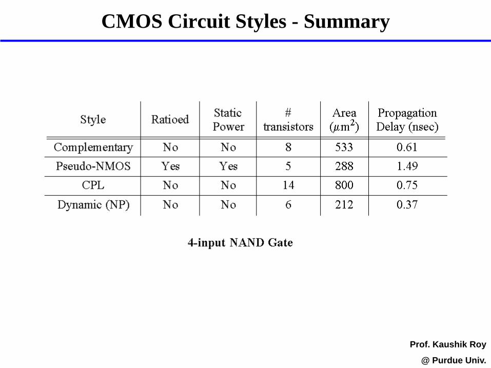
CMOS Circuit Styles - Summary
Prof. Kaushik Roy
@ Purdue Univ.