Combinational Circuit Analysis and Designzshi/course/cse2300/lecture4_comb.pdf · Combinational...
25
Combinational Circuit Analysis and Design Z. Jerry Shi Department of Computer Science and Engineering University of Connecticut CSE2300W:Digital Logic Design
Transcript of Combinational Circuit Analysis and Designzshi/course/cse2300/lecture4_comb.pdf · Combinational...
Combinational Circuit Analysis and Design
Z. Jerry ShiDepartment of Computer Science and Engineering
University of Connecticut
CSE2300W:Digital Logic Design

Combinational versus sequential
• Combinational circuit: the outputs depend on the current input values
• Sequential circuit: the outputs also depend on the history of inputs– Two identical sequential circuits may produce different outputs
even if their current inputs are the same
Examples?

Combinational circuit analysis
• Combinational circuits -- outputs depend only on current inputs (not on history)
• Types of combinational analysis:– Exhaustive (truth table)– Algebraic (expressions)– Simulation / test bench
• Write functional description in HDL• Define test conditions / test vectors, including corner cases• Compare circuit output with functional description (or known-good
realization)• Repeat for “random” test vectors

Combinational analysis
Record outputs generated on all input combinations.
You do not need to know the implementation details.

Constructing the truth table

Signal expressions
If you know the implementation details …

New circuit, same function
• Multiply out:F = ((X + Y′) ⋅ Z) + (X′ ⋅ Y ⋅ Z′)
= (X ⋅ Z) + (Y′ ⋅ Z) + (X′ ⋅ Y ⋅ Z′)
• Two-level AND-OR circuit

“Add out” logic function
• F = ((X + Y′) ⋅ Z) + (X′ ⋅ Y ⋅ Z′)= (X+Y′+X′) ⋅ (X+Y′+Y) ⋅ (X+Y′+Z′) ⋅ (Z+X′)⋅(Z+Y)⋅(Z+ Z′)= 1 ⋅ 1 ⋅ (X+Y′+Z′) ⋅ (X′+Ζ) ⋅ (Y+Z) ⋅ 1= (X+Y′+Z′) ⋅ (X′+Ζ) ⋅ (Y+Z)
• Two-level OR-AND circuit

Using symbol substitution directly

Cancelling bubbles
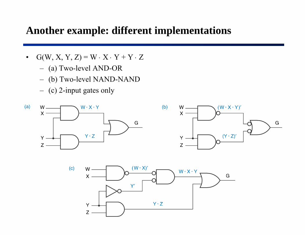
Another example: different implementations
• G(W, X, Y, Z) = W ⋅ X ⋅ Y + Y ⋅ Z – (a) Two-level AND-OR– (b) Two-level NAND-NAND– (c) 2-input gates only

Sum-of-products Form
AND-OR
NAND-NAND

Product-of-sums form
OR-AND
NOR-NOR
Sum-of-products preferred in CMOS and TTL (NAND-NAND)

One more example
A•B
B+C
B•C
B•C•(B + C)
= A•B+B•C•(B + C)

Reduction of logic expressions
A•B+B•C•(B + C)= A•B+B•C•B+B•C•C (T8: distributivity)= A•B+B•C+B•C (T3: Idempotency)= A•B+B•C (T3′: Idempotency)= B•(A+C) (T8: distributivity)

Combinational Circuit Design
• Sometimes you can write an equation or equations directly using “logic” (the kind in your brain).
• Example (alarm circuit):The ALARM output is 1 if the PANIC input is 1, or if the ENABLE input is 1, the EXITING input is 0, and the house is not sure; The house is secure if the WINDOW, DOOR, and GARAGE inputs are all 1

Alarm circuit derived from logic expression

Alarm Circuit Transformation
• Multiply out– Sum-of-products form (two-level AND-OR circuit)
• Useful for programmable logic devices

Brute-force design
• Truth table Canonical sum (Sum of minterms)
• Example: Design a circuit to detect prime numbers between 0-15
Given a 4-bit input, N3N2N1N0, produce a 1 output for N = 1, 2, 3, 5, 7, 11, 13 and a 0 otherwise
row N3 N2 N1 N0 F0 0 0 0 0 01 0 0 0 1 12 0 0 1 0 13 0 0 1 1 14 0 1 0 0 05 0 1 0 1 16 0 1 1 0 07 0 1 1 1 18 1 0 0 0 09 1 0 0 1 010 1 0 1 0 011 0 0 1 1 112 1 1 0 0 013 1 1 0 1 114 1 1 1 0 015 1 1 1 1 0
F = ΣN3, N2, N1, N0(1,2,3,5,7,11,13)

Minterm list Canonical sum

Algebraic simplification
• Theorem T10: X • Y + X • Y ' = X
• Reduce number of gates and gate inputs

Resulting circuit

More design examples
• Pass or failThere are three components in a course: homework (H), lab(L), and exam (E). You pass the course (P) only if you pass two or more components
• Compare two 1-bit numbersGiven two bits A and B, produce three signals G, L, and E so that G is 1 only when only when A > B, L is 1 only when A < B, and E is 1 only when A = B
• Compare two 2-bit numbersRepeat the comparison for two 2-bit numbers A = (A1, A0) and B = (B1, B0)
• Compare two 3-bit two’s complement numbersA = (A2, A1, A0) and B = (B2, B1, B0)

Delay of a combinational circuit
• The propagation delay of a signal path is the time that it takes for a change at the input of the path to produce a change at the output of the path– Many different paths from inputs to outputs– Different delays for LOW to HIGH and HIGH to LOW changes
• Critical path: the path that has the longest delay

Design goals
• Function• Delay• Area• Power
• Testability• Reliability• Security