cmos - t Upongsak.ee.engr.tu.ac.th/le242/doc/cmos.pdf · CMOS Logic Gate Structure. CMOS Logic...
12
CMOS Technology CMOS Technology •NMOS •PMOS •CMOS •Logic Gates using CMOS •Logic Gates using CMOS •Layout 1
Transcript of cmos - t Upongsak.ee.engr.tu.ac.th/le242/doc/cmos.pdf · CMOS Logic Gate Structure. CMOS Logic...
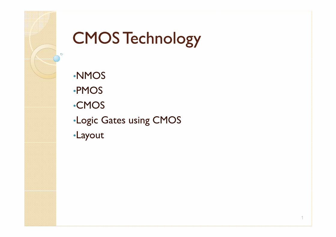
CMOS TechnologyCMOS Technology
•NMOS
•PMOS
•CMOS
•Logic Gates using CMOS•Logic Gates using CMOS
•Layout
1

NMOS StructureNMOS Structure� Gate (Metal -> Polysilicon)
� Insulator (Oxide -> Silicon dioxide)
� Substrate (Semiconductor : Si, SiGe)
2

NMOS OperationsNMOS Operations
3[Adapted from Fundamentals of Digital Logic by Brown & Vranesic]

PMOS structure & operationsPMOS structure & operations
4

SwitchSwitch--Level View of NMOS & Level View of NMOS & PMOSPMOS
[Adapted from Principles of CMOS VLSI Design by Weste & Eshraghian]
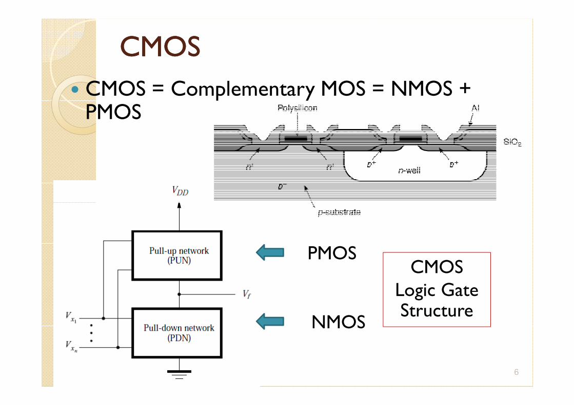
CMOSCMOS
� CMOS = Complementary MOS = NMOS + PMOS
6
PMOS
NMOS
CMOS Logic Gate Structure

CMOS Logic GatesCMOS Logic Gates
7
InverterNAND NOR

Required ConditionsRequired Conditions
� NAND:
◦ PUN : consider f = 1 (i.e., f= (x1 x2)’) when x1 = 0
or x2 = 0, thus inputs x1, x2 “in parallel”
◦ PDN : consider f = 0 (i.e., f’= x1 x2) when x1 = 1
and x2 = 1, thus x1, x2 “in series”and x2 = 1, thus x1, x2 “in series”
� NOR: the opposite to NAND
◦ PUN : consider f = 1 (i.e., f= (x1+x2)’) when both
x1 = 0 and x2 = 0, thus inputs x1, x2 “in series”
◦ PDN : consider f = 0 (i.e., f’= x1 +x2) when x1 = 1
or x2 = 1, thus x1, x2 “in parallel”
� Note that AND -> “series”, OR -> “parallel”.8

CMOS CircuitsCMOS Circuits
9
AND
321 xxxf +=

Stick Diagram & LayoutStick Diagram & Layout
10
Stick Diagram
Layout

CMOS CMOS Inverter LayoutInverter Layout
VDD
PMOS
1.2 µm=2λλλλ
Polysilicon
InOut
Metal
GND
NMOS
=2λλλλ
[Adapted from http://infopad.eecs.berkeley.edu/~icdesign/. Copyright 1996 UCB]

44--Input NAND GateInput NAND Gate
In1
In1 In2 In3 In4
VDD
Out
Vdd
In3
1
In2
In4
In1 In2 In3 In4
GND
Out
[Adapted from http://infopad.eecs.berkeley.edu/~icdesign/. Copyright 1996 UCB]