CMOS Schmitt Trigger Test Circuit Mitchell Belser, P.E. Visiting Instructor Department of Computer...
21
CMOS Schmitt Trigger Test Circuit Mitchell Belser, P.E. Visiting Instructor Department of Computer Engineering Jackson State University [email protected]
Transcript of CMOS Schmitt Trigger Test Circuit Mitchell Belser, P.E. Visiting Instructor Department of Computer...

CMOS Schmitt Trigger Test Circuit
Mitchell Belser, P.E.Visiting Instructor
Department of Computer EngineeringJackson State University

What is a Schmitt Trigger
• A type of comparator.
• A comparator is an electronic circuit whose output state changes when its input reaches a certain value.
• A comparator’s output state will change at the same input value whether the input voltage is increasing or decreasing.
• A noisy signal can cause the output to change state randomly.

Schmitt Trigger Operation
• The Schmitt trigger is a comparator circuit that has two threshold voltages.
• When the input is higher than the upper threshold, the output is high.
• When the input is lower than the lower threshold, the output is low.

Schmitt Trigger Operation• The Schmitt trigger employs positive
feedback.• When the input is between the two
thresholds the output state does not change.
• The difference between the two thresholds is the hysteresis.

Schmitt Trigger Transfer Curve

Schmitt Trigger History
• The Schmitt trigger was first invented by Otto H. Schmitt in the 1934.
• Vacuum Tube based design.• A Thermionic Trigger, Journal of Scientific
Instruments, 15 January 1938 pg 24-26

Schmitt Trigger
V 2
2
3
1
V 1
2
3
1
R6
R7
R8
R9R10
v-m inus
input
v-p lus
Thermionic Trigger
output

Schmitt Trigger Implementations
• Comparator with positive feedback
• Bipolar transistor Schmitt trigger
• CMOS transistor Schmitt trigger

Comparator with Positive Feedback
U1
R11
R12
V inoutput
Comparator w ith Positive Feedback

Bipolar Schmitt Trigger
Upper switching point voltage:
Vth = R4/(R4+R3)*Vdd
Lower switching point voltage:Vtl = R4/(R4+R2)*Vdd Q 1
Q 2R1
R2 R3
R4 R5
vdd
input
output
BJT Schmitt Trigger
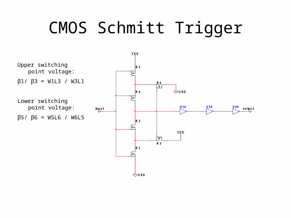
CMOS Schmitt Trigger
Upper switching point voltage:
β1/ β3 = W1L3 / W3L1
Lower switching point voltage:
β5/ β6 = W5L6 / W6L5
M 1
M 2
M 3
M 4
M 5
M 6
G ND
G ND
V DD
V DD
U1A U3A U4A outputinput

Applications
• Input buffers for digital signals.
• Crystal oscillator circuits.
• Clean up noisy signals (switch debounce).
• Speed up signals with slow edges.

Problem Description and Motivation for Improvement
The conventional method for characterizing a CMOS Schmitt trigger is to ramp up the input voltage until the output state changes. The input voltage that results in the output changing state is the high threshold voltage VTH. In a similar manner, the low threshold voltage VTL is determined by reducing the input voltage until a state change occurs at the output. This method is widely used. The major draw back is the time that is required to search for the input voltage that results in a state change at the output.
The proposed method would eliminate the need to perform a ramp search and thus greatly reduce the time needed to determine the switching threshold voltage levels.
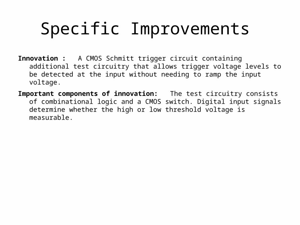
Specific Improvements
Innovation : A CMOS Schmitt trigger circuit containing additional test circuitry that allows trigger voltage levels to be detected at the input without needing to ramp the input voltage.
Important components of innovation: The test circuitry consists of combinational logic and a CMOS switch. Digital input signals determine whether the high or low threshold voltage is measurable.

Traditional Schmitt Trigger Circuit
M 1
M 2
M 3
M 4
M 5
M 6
G ND
G ND
V DD
V DD
U1A U3A U4A outputinput

Schmitt Trigger Showing Effect of Test Circuitry
►Test circuitry is shown in blue. ►Asserting test mode and vih input results in sout being shorted to the input. The gates of the feedback transistors are driven to vdd. The input is regulated to the high threshold voltage VTH.►Asserting test mode and vil input results in sout being shorted to the input. The gates of the feedback transistors are driven to gnd. The input is regulated to the low threshold voltage VTL.►In normal operating mode the test circuitry has no effect on Schmitt trigger operation.
M 1
M 2
M 3
M 4
M 5
M 6
G ND
G ND
V DD
V DD
U4A outputinput
U2A
7408J
U5A
7408J
U6A
7402N
U7A
7402N
U8A
7432N
V TL
V TH
Te st_e n
M 7 M 8 U1A
sout
soutsout
input

Advantages of This Method
Typical method requires input to be driven and output voltage to be monitored in order to determine the switching threshold voltage levels.
Test circuitry allow thresholds to be measured at the input without driving input or monitoring the output.
Simply setting a digital input causes the threshold voltage to be present on the input pin of the Schmitt trigger. .
Simplifies test program and reduces test time resulting in increased profit margin.
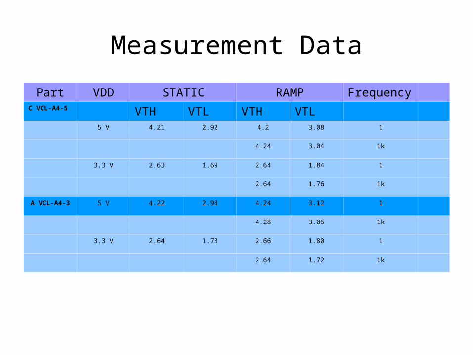
Measurement Data
Part VDD STATIC RAMP FrequencyC VCL-A4-5 VTH VTL VTH VTL
5 V 4.21 2.92 4.2 3.08 1
4.24 3.04 1k
3.3 V 2.63 1.69 2.64 1.84 1
2.64 1.76 1k
A VCL-A4-3 5 V 4.22 2.98 4.24 3.12 1
4.28 3.06 1k
3.3 V 2.64 1.73 2.66 1.80 1
2.64 1.72 1k

Measurement Waveforms
VDD= 3.3V
Ramp frequency = 1kHz

Summary
• Schmitt trigger threshold test circuit.• Measure rising and falling threshold levels.• Ramping input and monitoring output state is no
longer necessary.• Reduction in test time.• Increase in profit due to reduction in test time.