CMOS COMMUNICATIONS DEVICES - Vanderbilt...
163
SINGLE-EVENT CHARACTERIZATION AND MITIGATION IN HIGH-SPEED CMOS COMMUNICATIONS DEVICES By Sarah Elizabeth Armstrong Dissertation Submitted to the Faculty of the Graduate School of Vanderbilt University in partial fulfillment of the requirements for the degree of DOCTOR OF PHILOSOPHY in Electrical Engineering December 2011 Nashville, Tennessee Approved: Professor Lloyd W. Massengill Professor W. Timothy Holman Professor Michael L. Alles Professor Robert A. Reed Professor Stephen Buchner
Transcript of CMOS COMMUNICATIONS DEVICES - Vanderbilt...

SINGLE-EVENT CHARACTERIZATION AND MITIGATION IN HIGH-SPEED
CMOS COMMUNICATIONS DEVICES
By
Sarah Elizabeth Armstrong
Dissertation
Submitted to the Faculty of the
Graduate School of Vanderbilt University
in partial fulfillment of the requirements
for the degree of
DOCTOR OF PHILOSOPHY
in
Electrical Engineering
December 2011
Nashville, Tennessee
Approved:
Professor Lloyd W. Massengill
Professor W. Timothy Holman
Professor Michael L. Alles
Professor Robert A. Reed
Professor Stephen Buchner

ii
ACKNOWLEDGMENTS
This project was made possible through the fortuitous alignment of circumstances. First, the
fellowship from NSWC Crane allowed me the luxury of choosing my research topic. Next, the
Defense Threat Reduction Agency provided the seeds of the idea for this emerging research. And
finally, my advisor, Lloyd Massengill, led me to and encouraged me to pursue a topic in which I
was and am truly interested.
Dr. Massengill’s technical expertise, guidance, patience, and friendship throughout this
endeavor helped me survive the graduate school experience. He supported the project from “Plan
A” to “Plan Z” (or whatever plan we ended up with). Time spent in office hours sessions helped
tremendously. I couldn’t have picked a better advisor.
My committee, comprised of Tim Holman, Mike Alles, Robert Reed, and Steve Buchner,
exceeded my expectations with their valuable inputs throughout the process. Their perspectives
helped keep this project focused and manageable (as much as was possible). Their words of
support helped fuel the push to the end.
Without the encouragement of Dale McMorrow, I would not have considered application to
this fellowship program. His mentorship helped me at every stage of the graduate experience. I
appreciate all the time he spent with me on technical writing, experimental procedures, and wine
tasting.
Thanks to my family for their unconditional love and support. I am so fortunate to have been
given such a strong foundation. Thanks to Jonathan Hicks for his patience, motivation, and most
of all, partnership. He had no idea what he was getting into when he asked me out because I was
wearing a geeky t-shirt. Thanks to my outside friends for their understanding and cheerleading,

iii
even when they didn’t understand my motivation. I am grateful to Brian, Megan, Daniel, Ray,
Mike, Beth, David, Vishwa, and Jon along with the other past and present RER group members
for their collaboration in the classroom, research, and general debauchery.
Finally, thanks to the management of NAVSEA Crane and the Defense Threat Reduction
Agency for providing the many resources that made this research possible and to the Radiation
Effects Research Group and the faculty of the Department of Electrical and Computer
Engineering at Vanderbilt University for continued technical support and productive feedback.

iv
TABLE OF CONTENTS
ACKNOWLEDGMENTS .............................................................................................................. ii
LIST OF FIGURES ...................................................................................................................... vii
LIST OF TABLES ....................................................................................................................... xiv
LIST OF ABBREVIATIONS ........................................................................................................xv
I. INTRODUCTION ..................................................................................................................1
Organization of Dissertation ................................................................................................2
II. COMMUNICATIONS SYSTEMS ........................................................................................4
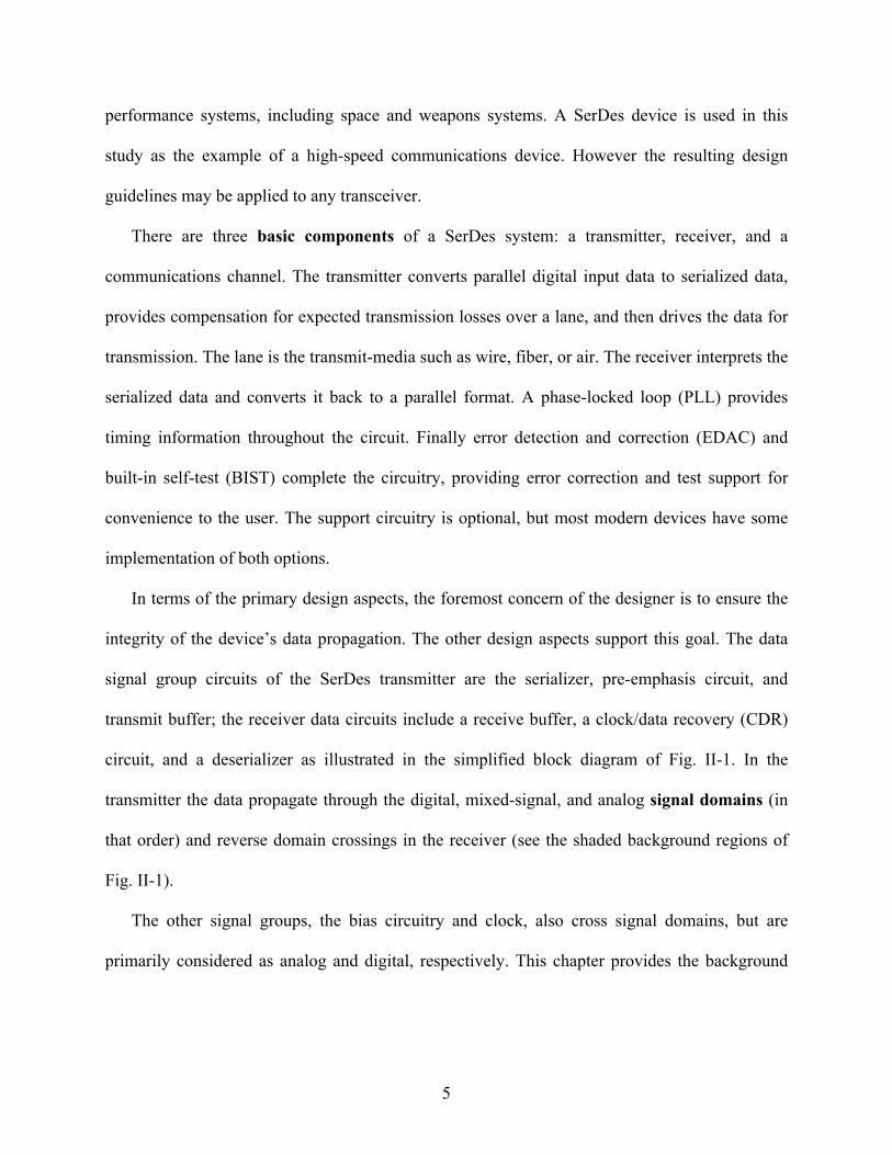
Introduction: A Systems Engineering View ........................................................................4 Signal Domains ....................................................................................................................6
Current Mode Logic .......................................................................................................7 Signal Groups.......................................................................................................................8
Data Flow .......................................................................................................................8 Timing and Power Circuits ..........................................................................................13
Protocols ............................................................................................................................14 XAUI ............................................................................................................................15
Environment .......................................................................................................................17 Single-Event Effects ....................................................................................................17 Single-Event Testing ....................................................................................................21
Conclusion .........................................................................................................................22
III. HIGH-SPEED MIXED-SIGNAL TRANSCEIVER CIRCUITRY ......................................24
Introduction ........................................................................................................................24 Data Flow Circuitry ...........................................................................................................25
Transmitter ...................................................................................................................25 Receiver .......................................................................................................................30
Timing and Power Circuitry ..............................................................................................33 Logic Timing and Clock Recovery ..............................................................................33 Bias Circuitry ...............................................................................................................36
Support Circuits .................................................................................................................37 Built-in-Self-Test (BIST) .............................................................................................37 Error Detection and Correction (EDAC) .....................................................................37
Conclusion .........................................................................................................................38

v
IV. SINGLE-EVENT CHARACTERIZATION VIA SIMULATION AND EXPERIMENT .....................................................................................................................39
Introduction ........................................................................................................................39 Establishing Error Criteria .................................................................................................40
Eye Diagram Masking .................................................................................................40 Error Criteria via Subcircuit Analysis ..........................................................................42
Single-Event Simulation ....................................................................................................44 Single-Event Laser Experiments ........................................................................................45 Analysis Tools Derived from Simulation and Experiment ................................................48
PDS Example ...............................................................................................................52 Conclusions ........................................................................................................................55
V. SINGLE-EVENT CHARACTERIZATION OF SELECT SERDES SUBCIRCUITS ........57
Introduction ........................................................................................................................57 Transmitter Circuits ...........................................................................................................58
Transmitter Simulation Results ....................................................................................60 6 dB Pre-Amplifier Experimental TPA Laser Results .................................................63 Transmit Buffer ............................................................................................................68 Transmitter OFF Signal ...............................................................................................68
Receiver Circuits ................................................................................................................70 Receiver Buffer ............................................................................................................70 Clock and Data Recovery ............................................................................................71 Comparator ..................................................................................................................78
Summary ............................................................................................................................80
VI. COMMON VULNERABILITIES IN SEE RESULTS OF SERDES CHARACTERIZATION ......................................................................................................81
CML Errors ........................................................................................................................81 CMOS-CML Interface .......................................................................................................82 Power and Bias Options .....................................................................................................82
VII. RADIATION-HARDENED-BY-DESIGN TECHNIQUES ................................................83
Introduction ........................................................................................................................83 Digital RHBD Techniques .................................................................................................84 Analog RHBD Techniques ................................................................................................85
Traditional Analog RHBD Techniques .......................................................................86 Charge Sharing RHBD Techniques .............................................................................86
Conclusions ........................................................................................................................97

vi
VIII. SINGLE-EVENT CHARACTERIZATION AND HARDENING OF CML CIRCUITS ............................................................................................................................98
Introduction ........................................................................................................................98 Pre-Amplifier CML Hardening ..........................................................................................98
PDS in Pre-Amplifier ...................................................................................................99 SEE Hardening of the Pre-Amplifier .........................................................................102 Phase Rotator .............................................................................................................104
Conclusions ......................................................................................................................109
IX. SINGLE-EVENT CHARACTERIZATION AND HARDENING OF DOMAIN INTERFACE CIRCUITS ...................................................................................................110
Introduction ......................................................................................................................110 Phase Rotator CML to CMOS .........................................................................................110
Clock and Data Recovery ..........................................................................................110 Comparator CML to CMOS with Clock ..........................................................................119 Pre-Amplifier CMOS to CML .........................................................................................121 Conclusions ......................................................................................................................123
X. RHBD GUIDELINES ........................................................................................................124
Guideline 1: RHBD in Signal Domain Interfaces ............................................................124 Guideline 2: RHBD in CML ............................................................................................126 Guideline 3: RHBD for Power Circuitry .........................................................................127
XI. CONCLUSIONS ................................................................................................................129
PUBLICATIONS .........................................................................................................................131
PRESENTATIONS .....................................................................................................................135
PROFESSIONAL ACTIVITIES .................................................................................................140
REFERENCES ............................................................................................................................141

vii
LIST OF FIGURES
Fig. II-1: Diagram of a basic SerDes consisting of a transmitter, a communication channel (lane), and a receiver. The clock, data path, and bias circuitry signal groups are identified with the respective signal domains: digital, mixed-signal, and analog. ...................................................6
Fig. II-2. Schematic of CML buffer. Key features are a differential input and controlled tail current (NMOS device controlled by “RFN”) and load (PMOS devices controlled by “RFP”). “RFN” controls the current flow, “RFP” controls the output swing. The output is not rail-to-rail and is most often converted to/from a full-rail signal to interface with standard CMOS logic. Figure from [Mu00]. ........................................................................................................................8
Fig. II-3. Example of the forward voltage gain characteristic (S21) degradation as a function of frequency for four path lengths on a typical PCB. FR-4 is an industry standard PCB material [Max08]. ...........................................................................................................................................9
Fig. II-4. A typical eye diagram with solid circles indicating the range of voltage margins and double circles showing the location of jitter measurements. In both cases, a “tight” grouping of signals is desirable over a “loose” grouping. Figure from [Wo08]. ..............................................10
Fig. II-5. Block diagram of a typical transmitter. The parallel data is serialized to half-rate into a series of flip-flops for emphasis. The signal is propagated to the lane after pre-amplification with gain as determined by the power DAC. Figure from [St08]. .........................................................11
Fig. II-6. Example of a receiver architecture. Data from the VGA are conditioned in the DFE block and the clock is recovered via the phase detector. Feedback from earlier data determines the amount of adjustment in both the phase rotator and the DFE block. Figure from [Bu06]. .....12
Fig. II-7: Extension of the 1000 Mb/s MAC sublayer to long-range 10 Gb/s data transmission by addition of the XGMII and the “Optional XGMII Extender” consisting of the indicated XGXS and XAUI blocks. Figure from [IEEE08] ......................................................................................16
Fig. II-8. Illustration of an ion strike on a reverse-biased n+/p junction [Bau05] ........................19
Fig. II-9. Diagram of a typical transient resulting from an ion strike on a reverse-biased n+/p junction [Ma93] .............................................................................................................................19
Fig. II-10. Illustration of an ion strike charge cloud in an older CMOS technology and a sub-100 nm CMOS technology. Note that several devices in the sub-100 nm technology are affected by the charge cloud [Am08]. ..............................................................................................................20
Fig. III-1. Diagram of a basic 8-bit serializer circuit. The large dashed box indicates the 8:2 serializer while the small dotted box indicates the clock dividers that provide a quarter-rate and eighth-rate clocks for the serialization logic. Figure from [St08]. .................................................26
viii
Fig. III-2. Example of a 2.488 Gbps signal showing ISI after transitions (left arrow) and CIDs (right arrow). Note that the first transition after the CID barely crosses the x-axis. Figure from [Max08]. .........................................................................................................................................27
Fig. III-3. Example of how equalization (or pre-emphasis) is tuned to cancel ISI. In this example, when the cable and equalizer are cascaded, the signal shows good linearity to 20 GHz. Figure from [Lu08]. ...................................................................................................................................28
Fig. III-4. A pre-emphasis circuit example shows flip-flops as delay generators and differential pairs to execute the emphasis. The feedback element including the loop filter is a simplified PLL, an element described later in this chapter. Figure from [Max08]. .................................................28
Fig. III-5. A data series demonstrating the application of pre-emphasis. In the bits following a transition, the signal is emphasized (voltage level is VOP). If there is no transition, the signal is not emphasized (voltage level is VO). Figure from [Max08]. ........................................................29
Fig. III-6. Overview of a DFE architecture. Figure from [Ema07]. .............................................31
Fig. III-7. Example of a 1:8 demultiplexing tree structure built from 1:2 DEMUX. The clock distribution network is connected to the select pins. Figure from [To06]. ....................................32
Fig. III-8. A 1:2 DEMUX circuit topology for use in the tree structure in Fig. II-8. Figure from [To06]. ...........................................................................................................................................32
Fig. III-9. Block diagram of a basic PLL circuit. Figure from [Be05]. ........................................34
Fig. III-10. Block diagram of a single PLL clock generator with distributed clock to four transceiver lanes. Figure from [Sa08]. ...........................................................................................35
Fig. III-11. Phase-rotating CDR block diagram. Figure from [Sa08]. ..........................................36
Fig. IV-1: The XAUI eye diagram template provides a mask to evaluate errors. Any signal that falls within the shaded regions is considered an error. This figure, along with Table IV-1 are used to define error characteristics in subsequent chapters. Figure from [IEEE08]. .............................41
Fig. IV-2: CDR block diagram for illustration of error criteria via subcircuit analysis. ...............43
Fig. IV-3: Five sample transients from a single point in a scan of a differential amplifier. The oscilloscope is triggered by an output generated by the laser system, with the laser clock and data stream operating in an asynchronous fashion. The time of the event is predictable, but the timing with the clock-cycle of the DUT is not. The y-axis scale is to determine relative magnitude, the traces are all centered around zero. ................................................................................................47
Fig. IV-4: Example of a simulated system WOV. The bottom figure shows the conversion cycle for a system. The top figure shows the source of errors or upsets, the number of nodes that elicit that response, and the duration with respect to the conversion cycle for which the error is likely. The proposed technique will enable an easy method to experimentally extract similar information from high-speed devices. Figure from [Kau04]. ............................................................................50
ix
Fig. IV-5: Schematic diagram illustrating the process for determining the strike time in the clock cycle. The time difference between the zero crossing (left vertical line) and the laser strike time (right vertical line) defines the phase relationship of each trace relative to the error injection and is determined by a computer scripted process. ..............................................................................51
Fig. IV-6: Three traces lined up in phase to directly illustrate the difference in response with laser strikes at different times in the data cycle. The vertical lines indicate the time of the laser strike for each individual trace. The times between the aligned zero crossing and the respective strike are collected for further analysis. .........................................................................................51
Fig. IV-7: Distribution of strike times over the data cycle. Taken from a TPA test of the 6 dB pre-amplifier circuit shown in Fig. V-3. ........................................................................................52
Fig. IV-8: (a) TPA scan showing phase-displacement results for the PLL. The right-most NMOS output switch is the source of the presented data. Figure from [Lov10]. (b) Schematic of charge pump indicating output switches and current sources. ..................................................................53
Fig. IV-9: Number of errors with respect to cycle time for NMOS switches in a PLL. Note that the number of errors correlates to the rising and falling edges in the overlaid data cycle. ............55
Fig V-1: Block diagram of transmitter driver. The level shifter / pre-amp combinations provide equalization to the signal and prepare the data to conform to a selected transmission protocol. ..58
Fig. V-2: Simulated pre-emphasis and buffer schematic. DiffAmp_A and DiffAmp_B correspond to T0/T1 and T9/T10, respectively, of the experimental device. ................................59
Fig. V-3: Simplified 6 dB pre-amp used in experiments. T0/T1 and T9/T10 are the differential amplifiers, T2/T3 is the output stage, and the current mirror includes each of the transistors at the bottom of the figure. The current drive increases from left to right on the schematic. Unlike the simulated device, the bias point is set off-chip. .............................................................................60
Fig. V-4: Different input structures used in simulation (left) and experiment (right). The input data are current based in the simulation version and voltage based in the experimental version. .60
Fig. V-5: Typical bit error from simulation for a PMOS-strike on the 6 dB pre-amp input node. It can be seen that the struck transient (solid red line) deviates from the expected transient (dashed black line) and causes a significant difference (±20% change) in the bit period. Simulation is run at 1.56 Gb/s. ...................................................................................................................................61
Fig. V-6: Maximum phase displacement for the unhardened pre-amplifier circuit. The N-strike is on the Data_N node and the P-strike is simulated as striking the PMOS device at node T of Fig. V-2. Data in the shaded region is considered erroneous. ...............................................................62
Fig. V-7: CDF of unhardened pre-amplifier device at an LET of 40 MeV-cm2/mg. Approximately 50% of P-strikes will result in errors, while approximately 8% of N-strikes will result in errors. The N-strike is on the Data_N node and the P-strike is simulated as striking the PMOS device at node_T of Fig. V-2. Data to the right of the vertical line is in the error region. 63

x
Fig V-8: Differential input signal, a sinusoid with an operating frequency of 1.56 GHz, simulating a checkerboard data pattern (1, 0, 1, 0,…) ...................................................................64
Fig V-9: Layout view of 6 dB pre-amp indicating the primary areas of the circuit and annotating the threshold energies. ...................................................................................................................64
Fig. V-10: Illustration of bit error. An error occurs if the measured voltage level does not reach a percentage of the expected voltage level. This percentage is considered the error threshold. ......66
Fig. V-11. Sample transient for a bit upset in T0/T1 resulting from a laser pulse energy of 6.9 nJ. This is a typical example of the observed bit upsets throughout the circuit. The shaded region indicates the areas in which an error is identified. In this case, the error threshold is 50% of the average peak voltage. .....................................................................................................................67
Fig. V-12: Error maps of T9/T10 from two incident pulse energies, as indicated. An enlarged version of Fig. V-9 is shown for reference. Most sensitive regions begin to resolve in (b) with clear identification of the transistor structure shown in (a). ..........................................................68
Fig. V-13: Block diagram of simulated output structure for a SerDes circuit. ..............................69
Fig. V-14: Differential output transient of simulated SEE strike at the OFF node in Fig. V-10. The circuit recovers at 25 µs ..........................................................................................................70
Fig. V-15: Schematic of receiver buffer [Bu06]. ...........................................................................71
Fig. V-16: Block diagram of a typical receiver and CDR circuit. The CML to CMOS block converts the incoming PLL clock to CMOS logic for use in timing the CDR comparator. All signals are differential. ...................................................................................................................72
Fig. V-17: Phase rotator schematic ................................................................................................73
Fig. V-18: Maximum phase displacement for the CML mixer subcircuit of the phase-rotator shown in Fig. V-15. Points in the shaded region are considered errors. The hollow symbols indicates N-strikes, the filled symbol indicates P-strikes. .............................................................73
Fig. V-19: CDF for unhardened phase rotator. Phase displacements to the right of the vertical dotted line are considered errors. ...................................................................................................74
Fig. V-20: CML to CMOS circuit derived from [Ema07]. The limited swing of the CML inputs are translated to full-swing CMOS outputs through current-based data to a regenerative inverter pair. The CML inputs are received from the PLL clock that has been rotated to match incoming receiver data. The CMOS outputs are fed back into the CDR comparator to provide timing information. ....................................................................................................................................75
Fig. V-21: Maximum (top) and average (bottom) phase displacement for SE strikes. Results falling above the dashed line are considered errors. ......................................................................77

xi
Fig. V-22: Cumulative distribution function of likelihood of magnitude of phase displacement. Events to the right of the vertical line are considered errors. ........................................................77
Fig. V-23: Simulated schematic of comparator. Out_p and Out_n lead to latches that sample the value at the node using the rotated clock. The latched signals are compared with an XNOR gate to indicate an error. ........................................................................................................................78
Fig. V-24: Illustration of an error captured with the XNOR error signal (top) and an error missed by the XNOR gate (bottom). ..........................................................................................................79
Fig. VII-1. Block illustration of TMR (after [Bl02]) .....................................................................85
Fig. VII-2: The S/H amplifier is a commonly used differential switched-capacitor circuit. The dual-data path provides a large dynamic output range and high noise rejection and has several examples of “sister” differential transistors. ..................................................................................88
Fig. VII-3: Illustration of single-ended and fully differential operation. An injected transient on a single-ended amplifier will be propagated with the signal while a transient shared by the inputs of a fully-differential amplifier will be cancelled. .........................................................................89
Fig. VII-4: Proposed charge-sharing layout designs single (SX) (top) and unit-cell (PX) (bottom). The drains of the devices are placed as close as design rules allow. The transistor pairs are placed a common well. ..............................................................................................................................89
Fig. VII-5: Schematic diagram of test circuit and the RHBD PX layout. All capacitors in the schematic are 516 fF. Two non-overlapping clocks, PreCharge and S(enseAmp), are precisely timed with the laser repetition rate. ................................................................................................91
Fig. VII-6: Timing diagram for data collection. Voltages are set during pre-charge, the laser strikes, and then the state is evaluated (out 1 and out 2) when the sense-amp clock is active. Pulse widths are not to scale. Out 1 and out 2 are either on or off. .........................................................92
Fig. VII-7: Surface plots of charge collected at points in the die scan. Charge collected by a single transistor for each configuration, BLSX (left) and BLPX (right), is shown in the top row. Differential charge is shown in the bottom row for SX (left) and PX (right). ...............................94
Fig. VII-8: Distribution of collected charge versus device area. Shows the amount of area (x-coordinate) that collects an amount of charge (y-coordinate) or less in the device for each of the four scenarios from left to right: BLPX, BLSX, SX, PX. The total area for the SX and PX layouts is 46 µm2 and 49 µm2, respectively. ..................................................................................95
Fig. VII-9: Conceptual schematic of SNACC technique. A single-event strike to a sensitive node creates a current, ISET. SNACC provides a compensating current, ICOMP, generated through exploitation of the charge-sharing phenomenon. A strike on any area of the common layouts produces an opposite (and, ideally, equal) transient at the sensitive node. ...................................96
xii
Fig. VII-10: Bootstrap current source with SNACC applied. Transistors M7-M12 are the devices added for the SNACC technique. M1-M4 are the core bootstrap device and M5 and M6 make up start-up circuitry. Figure from [Bl10]. ...........................................................................................97
Fig. VIII-1: Simplified 6 dB pre-amp used in experiments. T0/T1 and T9/T10 are the differential amplifiers, T2/T3 is the output stage, and the current mirror includes each of the transistors at the bottom of the figure. The current drive increases from left to right on the schematic. Unlike the simulated device, the bias point is set off-chip. .............................................................................99
Fig. VIII-2. Sample transient for a bit upset in T0/T1 resulting from a laser pulse energy of 6.9 nJ. This is a typical example of the observed bit upsets throughout the circuit. The shaded region indicates the areas in which an error is identified. In this case, the error threshold is 50% of the average peak voltage. ...................................................................................................................100
Fig. VIII-3: Histograms of error counts superimposed on the data cycle for the outputs of a scan of the device operating at 2 Gbps with an incident laser energy of 4.6 nJ. OUTP (a) shows fewer errors overall than (b) OUTM due to excess noise on the OUTM signal. Errors are binned according to the time in the data cycle the laser struck the device. .............................................101
Fig VIII-4: Simulated transients at the outputs of the circuit in Fig. VIII-1 for strike conditions listed in Table VIII-1. The vertical line indicates the point of greatest excursion from the no-strike condition. ............................................................................................................................104
Fig. VIII-5: Phase rotator schematic with DCC sister devices identified. The transmission gate nodes are laid out as shown in Fig. VIII-6. The differential sister pairs are laid out in a similar fashion or as shown in Fig. VII-4. ...............................................................................................105
Fig. VIII-6: Example layout for transmission gate pairs. The schematic represents the circled transmission gates in Fig. VIII-5. The drains of the same-type devices are adjacent to promote charge sharing. .............................................................................................................................106
Fig. VIII-7: Maximum phase displacement for the N-strike (a) and P-strike (b) results for the CML subcircuit of the phase-rotator shown in Fig. V-15. Points in the shaded region are considered errors. The filled symbols indicate normal incidence simulations, the hollow symbols indicate simulated angled strikes. ................................................................................................107
Fig. VIII-8: CDF for DCC hardened phase rotator for N-strikes (a) and P-strikes (b). The left graph in each figure shows results for normal-incidence simulations, the right panel shows results for 60-degree incidence. Phase displacements to the right of the dotted line are considered errors. ...........................................................................................................................................108
Fig. IX-1: Block diagram of a typical receiver and CDR circuit (a). The CML to CMOS block converts the incoming PLL clock to CMOS logic for use in timing the CDR comparator. All signals are differential. CML to CMOS circuit (b) derived from [Ema07]. The limited swing of the CML inputs are translated to full-swing CMOS outputs through current-based data to a regenerative inverter pair. The CML inputs are received from the PLL clock that has been rotated to match incoming receiver data. The CMOS outputs are fed back into the CDR comparator to provide timing information. .........................................................................................................111

xiii
Fig. IX-2: Maximum and average phase displacement for SE strikes in the circuit hardened by increased currents along with the baseline results (small icons and dotted lines). Events above the dotted lines are considered errors. The results for net5 fall in line with net3. .............................113
Fig. IX-3: CDF for charge dissipation hardening scheme. The shift of the results to the left indicates an improvement in the hardening of the circuit. Events to the right of the vertical line are considered errors. ...................................................................................................................113
Fig. IX-4: CML to CMOS circuit with DCC devices indicated. The transistor pairs are laid out similar to a common-centroid layout, but ensuring the drains are as close in proximity as allowed by layout design rules. The circled area of the schematic indicates the design modification to promote common mode rejection. The resistor is 2 kΩ. ..............................................................114
Fig. IX-5: Maximum and average phase displacement results of DCC hardening at normal (a) and 60-degree angle (b). In all cases, improvement is seen over the unhardened circuit. Events above the dashed lines are considered errors. ..............................................................................117
Fig IX-6: CDF of DCC hardened circuit along with baseline results for normal strikes (a) and angled strikes (b). Events to the right of the vertical line are considered errors. .........................118
Fig. IX-7: Simulated schematic of comparator. Out_p and Out_n lead to latches that sample the value at the node using the rotated clock. The latched signals, Out_p and Out_n are compared with an XNOR gate to sense an error. .........................................................................................120
Fig. IX-8: Simulated pre-emphasis and buffer schematic. Data_P and Data_N are paired using the DCC technique as are Data_P/N and NodeT_P/N. ................................................................121
Fig. IX-9: Maximum phase displacement results for strikes on Data_P and Node A of the pre-amplifier shown in Fig. IX-X. ......................................................................................................122
Fig. IX-10: CDF plot for nodes Data_P and Node A for hardened and unhardened conditions. The inset figure shows a magnification of the upper-left corner of the larger figure. .................122
Fig. X-1: Pre-amplifier schematic with DCC sister devices identified. Device pairs ‘A’ and ‘B’ are related to the domain interface errors. Pairs ‘C’ and ‘D’ have DCC applied as part of CML hardening. .....................................................................................................................................125
Fig. X-2: Unhardened CML to CMOS circuit (left) and hardened circuit with DCC sister devices identified (right). Due to the cross-coupled current amplifier, the pairs are not always complementary devices of the differential signal. Also, modification from the original schematic makes DCC possible with device pair ‘F’. ..................................................................................126
Fig. X-3: Pre-amplifier circuit used in experiment with non-ideal biasing. When DCC is applied to differential pairs T0/T1 & T9/T10, the SE response is improved by 56%. .............................127

xiv
LIST OF TABLES
Table III-1: Matrix of circuits, their subcircuits, signal domain, and simulation information. Schematics of the simulated circuits are provided in Chapter V. ..................................................24
Table IV-1: Values for XAUI eye-diagram error template in reference to Fig. II-8. UI is the unit interval in seconds and is defined as a bit-width or half of the period of the operating frequency. For XAUI, a UI is nominally 320ps. ..............................................................................................41
Table V-1: List of simulated circuits. ............................................................................................57
Table V-2. Measured SerDes transmitter driver electrical performance ......................................59
Table V-3: Summary of number of upsets observed by circuit area. 6.9 nJ laser pulse energy. ...67
Table V-4: Unhardened comparator error count by node and strike-type. ....................................79
Table VII-1: Sensitive areas collecting differential charge greater than 100 fC for Baseline and DCC SX and PX ............................................................................................................................95
Table VIII-1: Simulated charge on T9 & T10 in each of the four scenarios ...............................103
Table VIII-2: Error count for phase rotator for DCC hardened and unhardened circuits. Node B is not simulated for P-strikes. ..........................................................................................................105
Table IX-1: Design penalties of charge dissipation (CD) and differential charge cancellation (DCC) RHBD techniques. ...........................................................................................................119
Table IX-2: Number of errors (phase displacements exceeding 80 ps) for unhardened, charge dissipation (CD), and DCC at normal (DCC0) and angled (DCC60) strikes. .............................119
Table IX-3: Number of errors for unhardened and hardened comparator at Data, Latch, and Output nodes for unhardened, normal strikes with DCC, and angled strikes with DCC. ...........121

xv
LIST OF ABBREVIATIONS
ASET................................................................................................ Analog Single-Event Transient BERT ............................................................................................................. Bit-Error Rate Testing
BIST ...................................................................................................................... Built-in Self-Test BLPX .................................................................................................... Baseline-Parallel Transistor
BLSX ...................................................................................................... Baseline-Single Transistor CD ....................................................................................................................... Charge Dissipation
CDF ............................................................................................. Cumulative Distribution Function CDR ......................................................................................................... Clock and Data Recovery
CID .......................................................................................................... Consecutive Identical Bits CM ............................................................................................................................. Current Mirror
CML ................................................................................................................. Current-Mode Logic CMOS ....................................................................... Complementary Metal-Oxide Semiconductor
CMRR ............................................................................................ Common-Mode Rejection Ratio coax .............................................................................................................................. Coaxial cable
DAC ...................................................................................................... Digital to Analog Converter DC .............................................................................................................................. Direct Current
DCC .............................................................................................. Differential Charge Cancellation DD ................................................................................................................. Displacement Damage
DEMUX ..................................................................................................................... Demultiplexer DFE ..................................................................................................... Decision Feedback Equalizer
DSET................................................................................................ Digital Single-Event Transient DUT .................................................................................................................... Device Under Test
EDAC ............................................................................................... Error Detection and Correction ESD .............................................................................................................. Electrostatic Discharge
FPGA ............................................................................................... File-Programmable Gate Array GS/s ........................................................................................................ Giga-Samples per Seconds
IC........................................................................................................................... Integrated Circuit IEEE ...................................................................... Institute of Electrical and Electronics Engineers
ISI ............................................................................................................. Inter-Symbol Interference ISO ......................................................................................... International Standards Organization

xvi
LC .................................................................................................................... Inductor/Capacatitor LET .............................................................................................................. Linear Energy Transfer
LVDS ........................................................................................... Low-Voltage Differential Signals MAC .............................................................................................................. Media Access Control
MBU ................................................................................................................... Multiple-Bit Upset MUX ............................................................................................................................... Multiplexer
OSI ..................................................................................................... Open System Interconnection PCB ................................................................................................................. Printed Circuit Board
PDK .................................................................................................................... Process Design Kit PDS ..................................................................................................... Phase-Dependent Sensitivity
PLL ................................................................................................................... Phase-Locked Loop PRBS ........................................................................................... Pseudo-Random-Binary Sequence
PX ........................................................................................................ Parallel-Unit-Cell Transistor RF ........................................................................................................................... Radio Frequency
RHBD .............................................................................................. Radiation-Hardened by Design SE .................................................................................................................................. Single Event
SEE .................................................................................................................... Single-Event Effect SerDes ............................................................................................................ Serializer/Deserializer
SET ............................................................................................................... Single-Event Transient SEU .................................................................................................................... Single-Event Upset
SNACC ........................................................................ Sensitive Node Active Charge Cancellation SONET ......................................................................................... Synchronous Optical Networking
SPA .......................................................................................................... Single-Photon Absorption SX .......................................................................................................................... Single-Transistor
TCAD ..................................................................................... Technology Computer-Aided Design TID ..................................................................................................................... Total Ionizing Dose
TPA .............................................................................................................Two-Photon Absorption TMR ..................................................................................................... Triple-Modular Redundancy
UI ................................................................................................................................ Unit Interface USB .................................................................................................................. Universal Serial Bus
VCO ................................................................................................... Voltage Controlled Oscillator VGA ........................................................................................................... Variable Gain Amplifier
WOV ......................................................................................................... Window of Vulnerability

xvii
XAUI ..................................................................................... 10-Gigabit Attachment Unit Interface XGMII ............................................................................... 10-Gigabit Media Independent Interface
XGXS ...................................................................................................... XGMII Extender Sublayer XNOR ...................................................................................................................... Exclusive NOR

1
CHAPTER I
INTRODUCTION
Modern electronics provide the luxury of instant worldwide connectivity. In fact, this
connectivity is ingrained in modern society to an extent that near-perfect performance is
expected and perhaps taken for granted. People encounter high-speed communications circuits
daily through the use of wired or wireless technology connected to many types of
communications hubs, from global satellites to integrated circuits, whether it is for
entertainment, daily business interactions, or military operations. Therefore, the ability to
reliably transmit data at high speeds is critical to all modern communication devices. In order to
meet this need, high-speed serial communication protocols have been developed – the common
universal serial bus (USB) is a ubiquitous, though somewhat dated, example. Failure to meet
reliability specifications can be inconvenient, at best, and catastrophic, at worst.
From a system design point-of-view, four primary aspects of a communications system must
be taken into account: data flow, power, timing, and the actual operating environment. Of these,
the physical environment drives choices in circuit architecture to optimize the performance with
respect to data transmission, power consumption, and timing. There are design considerations for
most practical operating environments outside a controlled laboratory – from the obvious
challenges of satellite design in terms of extreme temperature operating range and exposure to
space radiation [He99] to the less-obvious high-temperature and terrestrial radiation
environments faced by personal computers or a video gaming systems [May79]. This dissertation
focuses on the radiation hazards facing high-speed communications devices in a space

2
environment - more specifically, the mitigation of single-event effects (SEE) in analog/RF
communications circuits. The consequence of failure to mitigate SEE could be the inconvenience
of having to re-send data or voice packets (which also results in wasted power) or, more
dramatically, the device could be temporarily or permanently disabled [Lad07].
The mix of signal domains on a single transceiver integrated circuit (IC) presents design
challenges that are compounded when radiation robustness is considered. The outcome of this
thesis is a set of guidelines for single-event (SE) radiation-hardening-by-design (RHBD) of a
high-speed communications device. A serializer/deserializer (SerDes) device is used in this study
as the example high-speed communications device. However, the resulting guidelines may be
applied to any transceiver.
The primary objective of this research is to first, distinguish global signal groups and signal
operating domains in high-speed communication devices in order to introduce a framework
around which SEE RHBD tactics can be shaped. Then, using the knowledge of the system as a
whole, hardening solutions are applied with minimal impact on the primary design
considerations.
Organization of Dissertation
The research effort proposed in this dissertation is organized as follows:
1) Chapter I introduces the motivation and objective of this work.
2) Chapters II, III, and IV provide background on communication systems, common
serializer/deserializer (SerDes) circuits, single-event effects, and

3
simulation/experimental techniques. Each section emphasizes the information
pertinent to this dissertation.
3) Chapters V – IX discuss the characterization of errors in the SerDes circuitry, identify
common vulnerabilities in the mixed-signal domain, and employ RHBD techniques to
mitigate SEE due to those vulnerabilities.
4) Chapters X and XI provide RHBD generalized guidelines for the design of high-
speed communication devices and concluding remarks.
Appendices A, B, and C list to-date publications, presentations, and involvement in the
radiation effects community, respectively.

4
CHAPTER II
COMMUNICATIONS SYSTEMS
Introduction: A Systems Engineering View
In general, when a high-speed transceiver system is considered as a whole, the following
predominant signal groups1 can be identified: the data path, bias circuitry (including the power
supply), and the clock. These in turn can be linked to three of the primary design aspects of
system design: data propagation, power consumption, and timing, respectively. The fourth
aspect, the operating environment, dictates special design considerations if the in-situ conditions
are expected to be harsh with respect to temperature or radiation. For the purposes of this work, a
harsh environment refers to the high probability of the device experiencing single-event effects
(SEE) such as in a space environment.
The enabling integrated circuit for the continued advancement of high-speed and high-
performance serial communication is the serializer/deserializer (SerDes) class of devices. The
transmission of parallel data requires the same number of pads and dedicated transmission lines
as bits to be transmitted. The power required to drive separate data paths and the spacing
required to prevent line-to-line interference are two of the major limiting factors in transmitting
digital parallel data. Serial data, when transmitted as a differential signal, provides fast and
accurate data transmission on par with parallel, but has advantages in terms of power
consumption and physical space required.
SerDes provide fast data transfers (in excess of 10 Gbps) across chip-to-chip, board-to-board,
and backplane interfaces. These circuits have become essential building blocks for high
1 Phrases in bold in this chapter are to highlight terminology to be used throughout the document to minimize confusion.
5
performance systems, including space and weapons systems. A SerDes device is used in this
study as the example of a high-speed communications device. However the resulting design
guidelines may be applied to any transceiver.
There are three basic components of a SerDes system: a transmitter, receiver, and a
communications channel. The transmitter converts parallel digital input data to serialized data,
provides compensation for expected transmission losses over a lane, and then drives the data for
transmission. The lane is the transmit-media such as wire, fiber, or air. The receiver interprets the
serialized data and converts it back to a parallel format. A phase-locked loop (PLL) provides
timing information throughout the circuit. Finally error detection and correction (EDAC) and
built-in self-test (BIST) complete the circuitry, providing error correction and test support for
convenience to the user. The support circuitry is optional, but most modern devices have some
implementation of both options.
In terms of the primary design aspects, the foremost concern of the designer is to ensure the
integrity of the device’s data propagation. The other design aspects support this goal. The data
signal group circuits of the SerDes transmitter are the serializer, pre-emphasis circuit, and
transmit buffer; the receiver data circuits include a receive buffer, a clock/data recovery (CDR)
circuit, and a deserializer as illustrated in the simplified block diagram of Fig. II-1. In the
transmitter the data propagate through the digital, mixed-signal, and analog signal domains (in
that order) and reverse domain crossings in the receiver (see the shaded background regions of
Fig. II-1).
The other signal groups, the bias circuitry and clock, also cross signal domains, but are
primarily considered as analog and digital, respectively. This chapter provides the background

6
information and terminology for signal domains, signal groups, and supplementary information
regarding protocols and environments.
Fig. II-1: Diagram of a basic SerDes consisting of a transmitter, a communication channel (lane), and a receiver. The clock, data path, and bias circuitry signal groups are identified with the respective signal domains: digital, mixed-signal, and analog.
Signal Domains
High-speed communications devices are comprised of mixed-signal circuitry. The digital
rail-to-rail serialized data in a SerDes are prepared for transmission over the analog
communications channel by converting the digital signal to current-mode logic (CML) in a pre-
emphasis circuit and an output buffer. A signal that is transitioned from one domain to another is
considered to have “crossed domains”. The intersection of signal domains is called a “domain
interface”.
CDR circuits have multiple domain interfaces because they handle the extraction and
retiming of the data, and in the process, the conversion from analog to digital signals. The signals
that cross domains include the data path of the receiver and the clock signal from the PLL to the
!"#$%
!"#$%&'()*)'
+,$#-,./'
0.,1'2345)676'
+,$,7-,'89:,.'
;.)<637*'89:,.'
(7=7*)"' (7=7*)"'><)"#=' ?7@,A1B7=<)"'?7@,A1B7=<)"'
!"#$%& !"#$%&'()*& '()*&
&'"#()*+$'% ,$-$*.$'%
B,.7)"7C,.' (,6,.7)"7C,.'
()*)'!'()*)'!'
()*)'!'

7
CDR. The CDR must convert the incoming analog data and the embedded clock signal from
analog to the rail-to-rail digital domain to have an accurate back-conversion to parallel data. The
system clock signal from the PLL used in the CDR is implemented in CML and must be
converted to a full-swing digital clock for synchronization with the clock embedded in the
received data.
One of the foci of this dissertation is SEE at domain interfaces. Of particular interest are the
conversion from full-swing CMOS to CML and vice-versa described above. In general, signals
that do not cross domains, specifically, the serializer and deserializer circuits and the clocks
directly associated with their operation, will not be discussed in depth. CML is discussed in the
following section to familiarize the reader with this lesser-known logic family.
Current Mode Logic
CML is widely used in high-speed CMOS design because of the benefits in speed, power
consumption, and noise reduction provided by the differential architecture. Figure II-2 shows a
schematic diagram of a typical CML buffer. The key features are the differential-pair inputs and
the tail current controlled by the bias reference. The differential inputs allow for excellent
common-mode noise rejection. The loading devices limit the output voltage swing, which, in
turn, allows for a faster switching time as compared to standard CMOS logic. The tail current is
adjustable and can control the dynamic power consumption. More information on CML circuit
design can be found in [Ali05].

8
Fig. II-2. Schematic of CML buffer. Key features are a differential input and controlled tail current (NMOS device controlled by “RFN”) and load (PMOS devices controlled by “RFP”). “RFN” controls the current flow, “RFP” controls the output swing. The output is not rail-to-rail and is most often converted to/from a full-rail signal to interface with standard CMOS logic. Figure from [Mu00].
Signal Groups
Data Flow
The primary data path through a SerDes is from the transmitter to the receiver via the
communication channel. Power and clock circuitries influence the integrity of the path, but the
data signal propagates through the dedicated circuitry. This section describes the basic data path,
first highlighting the communication channel, because its characteristics, along with
environmental restrictions, drive architecture decisions of the transmitter and receiver. The
general operation of a typical transmitter and receiver are briefly discussed.
Communication Channel
The communication channel is the path over which the signal is transmitted. The medium of
the channel may be a printed circuit board (PCB) trace, fiber cable, coaxial cable (coax), air, or
9
others. The individual media have benefits and drawbacks, typically with a cost versus
performance tradeoff.
Non-idealities in a transmission line must be accounted for in the design of transmitter and
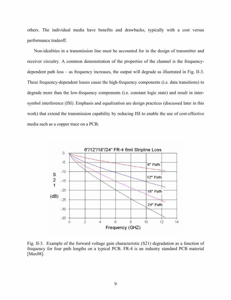
receiver circuitry. A common demonstration of the properties of the channel is the frequency-
dependent path loss – as frequency increases, the output will degrade as illustrated in Fig. II-3.
These frequency-dependent losses cause the high-frequency components (i.e. data transitions) to
degrade more than the low-frequency components (i.e. constant logic state) and result in inter-
symbol interference (ISI). Emphasis and equalization are design practices (discussed later in this
work) that extend the transmission capability by reducing ISI to enable the use of cost-effective
media such as a copper trace on a PCB.
Fig. II-3. Example of the forward voltage gain characteristic (S21) degradation as a function of frequency for four path lengths on a typical PCB. FR-4 is an industry standard PCB material [Max08].
10
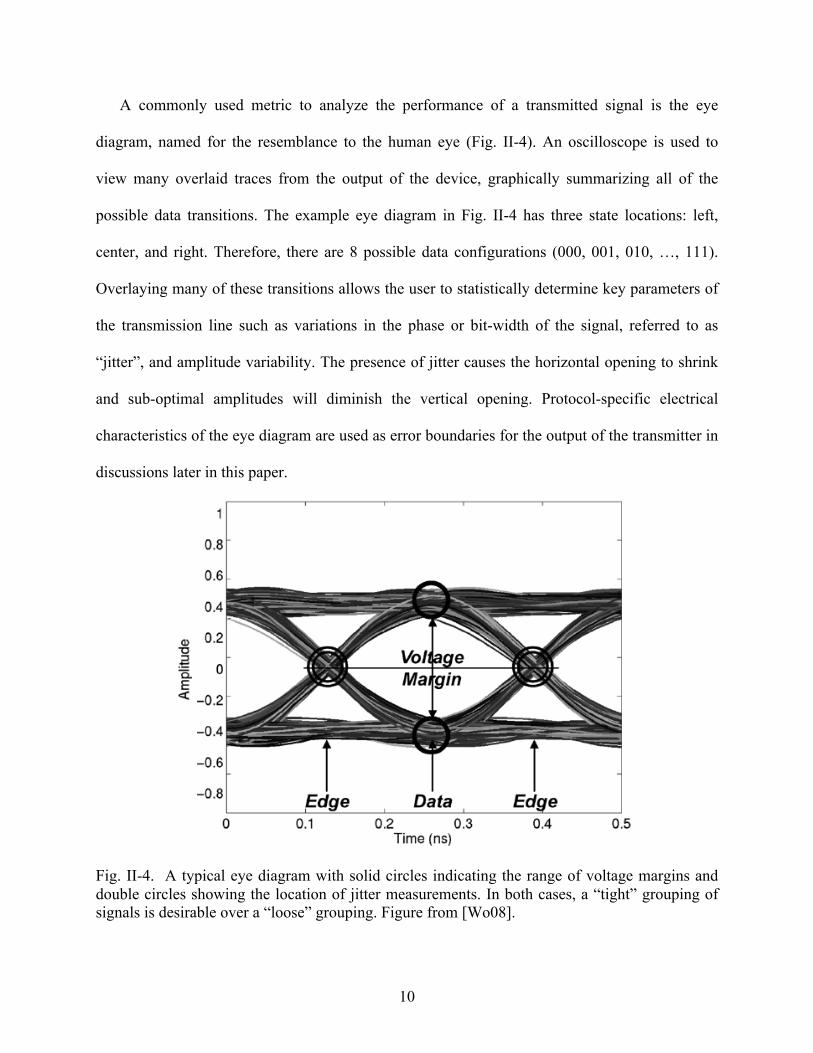
A commonly used metric to analyze the performance of a transmitted signal is the eye
diagram, named for the resemblance to the human eye (Fig. II-4). An oscilloscope is used to
view many overlaid traces from the output of the device, graphically summarizing all of the
possible data transitions. The example eye diagram in Fig. II-4 has three state locations: left,
center, and right. Therefore, there are 8 possible data configurations (000, 001, 010, …, 111).
Overlaying many of these transitions allows the user to statistically determine key parameters of
the transmission line such as variations in the phase or bit-width of the signal, referred to as
“jitter”, and amplitude variability. The presence of jitter causes the horizontal opening to shrink
and sub-optimal amplitudes will diminish the vertical opening. Protocol-specific electrical
characteristics of the eye diagram are used as error boundaries for the output of the transmitter in
discussions later in this paper.
Fig. II-4. A typical eye diagram with solid circles indicating the range of voltage margins and double circles showing the location of jitter measurements. In both cases, a “tight” grouping of signals is desirable over a “loose” grouping. Figure from [Wo08].

11
Transmitter The transmitter is comprised of three basic functions: the serializer, emphasis, and driver.
Figure II-5 shows a block diagram of a typical transmitter. In this figure, encoded parallel data
are fed into the 8:2 serializer, which outputs half-rate data in form of “even” and “odd” bits. The
half-rate serialized data is combined via a 2:1 MUX and advanced to a series of flip-flops to
provide a primary, pre-cursor, and post-cursor data bit for pre-emphasis. The emphasis accents
any high-frequency component of the signal, that is, it emphasizes a state change. These bits are
combined at the output node after pre-amplification with the gain determined by the power
digital to analog converter (DAC). The emphasized signal is then driven over the backplane. The
output driver is not shown in the figure.
Fig. II-5. Block diagram of a typical transmitter. The parallel data is serialized to half-rate into a series of flip-flops for emphasis. The signal is propagated to the lane after pre-amplification with gain as determined by the power DAC. Figure from [St08].

12
Receiver The receiver is comprised of four basic functions: receive amplifier, equalization, data
recovery, and deserializer (Fig. II-6). Data is received from the transmit media, conditioned for
equalization and data recovery through a T-cell (used to aid in signal integrity over the
communications channel and ESD protection) and a variable gain amplifier (VGA). The output
of the VGA leads to the phase detector to begin the clock and data recovery (CDR) process and
the decision feedback equalizer (DFE) to adjust the signal to compensate for losses in the lane.
The phase rotator adjusts the clock from an external PLL to match the embedded clock through
the I-clock control and Q-clock control taps with values determined from previous data. After the
data are conditioned in the DFE block, they are deserialized. The output of the circuit provides
feedback for adjustments in equalization and data recovery. In addition, error correction may be
available, but is not shown in the figure.
Fig. II-6. Example of a receiver architecture. Data from the VGA are conditioned in the DFE block and the clock is recovered via the phase detector. Feedback from earlier data determines the amount of adjustment in both the phase rotator and the DFE block. Figure from [Bu06].

13
Timing and Power Circuits
The timing and power circuitries are the primary keys to preserving the integrity of data
throughout the SerDes system because they determine the sampling point in the data cycle for
synchronization and the speed of data transition. The overall power consumption of the circuit is
determined by these signal groups. The timing circuits include those that distribute the clock in
the transmitter and generate and recover the clock in the receiver. The power circuits are defined
as those that provide bias throughout the system. The power rail and associated stabilizing
circuitry are included in the power circuitry classification, but are not discussed in this paper.
The transmitter and receiver typically have separate timing circuits. The transmitter utilizes
an external clock operating at the transmission frequency (baud-rate) that provides the clock for
the serialization process and for the emphasis circuit. The purely digital transmitter clock
distribution circuit is not discussed in this paper because it does not cross signal domains.
Receiver-side timing requires recovery of the clock signal embedded in the received data. The
clock and data recovery circuit adjusts the phase of the clock to sample the data at the optimal
position in the signal.
The current drive through a circuit determines the overall power consumption of the circuit
and controls the speed of the device. Bias circuitry includes the bias generators and all related
current mirrors. In some cases, the current reference is set off-chip. In other cases, current
mirrors distribute a bias tree extensively through the circuit.

14
Protocols
Communications protocols are established to ensure electrical and mechanical compatibility
from device-to-device regardless of the manufacturer. These protocols dictate the encoding
scheme, frequency, and output voltage of the device and therefore, often determine circuit
architecture. 10-Gb Ethernet, Synchronous optical networking (SONET), and universal serial bus
(USB) are common examples of device protocols.
When a user interacts directly with software through computer applications, those
interactions must be translated to a signal that is transmitted as an electrical signal over a
medium. The International Standards Organization’s (ISO) Open System Interconnection (OSI)
model (described in the user-friendly document of [Zim80]) divides the translation from software
applications to a transmitted or received physical signal into seven “layers” (see the left “stack”
in Fig. II-7). This work focuses on the data link layer and the connection to the physical layer.
Normally, in the IEEE 802.3 communications standard, the data link layer consists of the media
access control (MAC) sublayer and some associated control structures. The MAC prepares data
packets from the network layer for transmission over the medium at the physical layer. The
baseline operating frequency of the MAC is 1000 Mb/s, a relatively slow baud-rate for modern
communications.
10-Gb Ethernet is a protocol that accelerates the IEEE 802.3 MAC sublayer from 1000 Mb/s
to 10 Gb/s. This is accomplished through the use of a 10-Gigabit Media Independent Interface
(XGMII), which is inserted between the MAC and the physical layer. The XGMII uses
independent transmit and receive signals in the form of 37 parallel signals in each direction (32
data bits, 4 control bits, and a clock signal). This parallel data transmission is limited in physical

15
range because of complications in skew and crosstalk. In cases where a signal is transferred over
a long distance (e.g. from chip-to-chip on a printed circuit board), an XGMII Extender is
implemented to extend data transmission beyond the distances of the XGMII. The extender
consists of four lanes that receive data divided by the XGMII, each lane includes a XGMII
Extender Sublayer (XGXS) and a 10-Gigabit Attachment Unit Interface (XAUI). Each lane
operates at 2.5 Gbps and together allow data transmission up to 50 cm [IEEE08]. Figure II-7
illustrates these connections and extensions. The XAUI electrical characteristics are the target
transmission characteristics for this dissertation.
XAUI
The 10-Gb attachment unit interface (XAUI) is designed to extend the transmission distance
of the 10-Gb Ethernet protocol. The XAUI is used as the example electrical standard of this work
because it is commonly used in commercial, military, and space applications. The protocol
definitions for amplitude and bit-width establish error criteria for the transmission circuits and
will be discussed in Chapter IV.
The data are encoded in the XGXS block to prepare for transmission by ensuring DC balance
and to provide an embedded clock for timing information in the receiver. DC balance ensures the
number of transmitted ‘0’s and ‘1’s is essentially equal to prevent an accumulated DC offset and
provides sufficient state changes to allow for accurate clock recovery. Accumulated DC offset
can cause headroom problems in the driver and can “clip” the signal. State changes are necessary
in clock recovery because the data edges drive the voltage-controlled oscillator (VCO) into lock
and insufficient transitions will cause the VCO to lose lock.
16
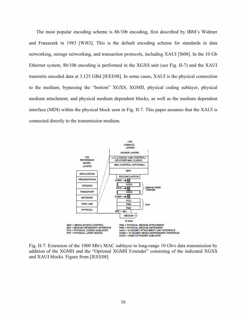
The most popular encoding scheme is 8b/10b encoding, first described by IBM’s Widmer
and Franaszek in 1983 [Wi83]. This is the default encoding scheme for standards in data
networking, storage networking, and transaction protocols, including XAUI [St08]. In the 10 Gb
Ethernet system, 8b/10b encoding is performed in the XGXS unit (see Fig. II-7) and the XAUI
transmits encoded data at 3.125 GBd [IEEE08]. In some cases, XAUI is the physical connection
to the medium, bypassing the “bottom” XGXS, XGMII, physical coding sublayer, physical
medium attachment, and physical medium dependent blocks, as well as the medium dependent
interface (MDI) within the physical block seen in Fig. II-7. This paper assumes that the XAUI is
connected directly to the transmission medium.
Fig. II-7: Extension of the 1000 Mb/s MAC sublayer to long-range 10 Gb/s data transmission by addition of the XGMII and the “Optional XGMII Extender” consisting of the indicated XGXS and XAUI blocks. Figure from [IEEE08]

17
Environment
In some cases, a device is to be used under harsh conditions that, in turn, drive the topology
of device design. These environments include exposure to extreme temperature swings,
consistently high or low temperature operation, and/or potential radiation exposure. This study
focuses on radiation effects, more specifically, single-event effects (SEE) on communications
systems.
The issues involved with the effects of radiation on electronics are many, particularly in the
case of space-deployed systems. Circuit-level effects include displacement damage (DD), total-
ionizing dose (TID), prompt dose (dose rate), and single-event effects (SEE). To encompass all
of these concerns in detail would be not only futile, but also redundant, as there is a rich
literature pool from which to draw. This chapter introduces background material for SEE in
SerDes devices, the focus of the radiation-effects analysis presented in this paper. For
information on the other topics, the ambitious reader may consult [Sr03], [Bar05], and [Al03] for
DD, TID, and prompt dose, respectively.
Single-Event Effects
Single event effects are the interaction of a single particle that causes a disturbance in a
circuit or system. The primary particles of concern for a space environment are heavy ions,
protons, alpha particles, and electrons. Effects of ion interactions in space environments are
typically observed as a result of cosmic ions, solar flares, products of secondary interactions, or
from natural radiation decay [Ba03].

18
Device scaling to the nano-scale is causing SEE at commercial flight altitudes and even
terrestrially. Neutrons are the primary causes for radiation-effects concerns within the Earth’s
atmosphere. As part of the hardening plan for terrestrial environments, the designer, must also
consider particles originating from device own packaging (alphas) and passivation (Boron
isotopes) along with other heavy ions, protons, electrons, muons, and pions, [Ba03].
There are three steps to a SE: charge generation, charge recombination and collection, and
circuit response. As the incident ion moves through the semiconductor, carriers are generated
and may directly affect a circuit’s operation directly through Columbic interactions or indirectly
through nuclear reactions with the lattice. In direct ionization, a path of electron-hole pairs is
generated by the energy of the ion exciting electrons to the conduction band. Indirect ionization
involves a collision of particles resulting in a nuclear reaction that may cause scattering or
spallation. The energy loss of the incident ion is referred to linear energy transfer (LET). More
formally, LET is the energy loss per unit length normalized by the density of the target material,
typically described in units of MeV-cm2/mg or pC/µm.
During charge collection, the generated charge is moved via drift and diffusion. Near a p-n
junction, the built-in electric field causes drift current – holes and electrons to be swept into the
p- and n-regions, respectively. This current is only present for a picosecond-scale time period,
and is limited by the number of excess carriers in the material [Bau05]. Figure II-8 illustrates this
concept. On the other hand, in the absence of an electric field, but within a diffusion length of a
junction, the diffusion process dominates. This process takes on order of hundreds of
picoseconds to nanoseconds. The effect of a SE with respect to time involves fast (drift) and
slow (diffusion) components as illustrated in Fig. II-9. The total charge is the integral of the
current over time [Ma93].

19
Fig. II-8. Illustration of an ion strike on a reverse-biased n+/p junction [Bau05]
Fig. II-9. Diagram of a typical transient resulting from an ion strike on a reverse-biased n+/p junction [Ma93]
The understanding of the effects of collected charge on the circuit is the key to successful
radiation-hardened-by-design (RHBD) implementation. The collected charge will cause a

20
disruption of nodal voltages and may affect normal circuit operation. In memories and sequential
logic, this disruption may be in the form of a single-event upset (SEU), where a “1” goes to “0”
or a “0” goes to “1” without permanent damage to the circuit. The erroneous bit can be corrected
or, but if left undetected, it may lead to a system malfunction. A single-event transient (SET) is
the result of the disruption in combinational logic or analog circuitry, called digital SET (DSET)
or analog SET (ASET), respectively. The consequence of SETs on circuitry depends on the
specific application of the device. A SEU may result if the transient exceeds the threshold of the
application in magnitude and/or duration [Ma93].
In an increasing number of cases, a single ion can generate more than one bit error causing a
multiple-bit upset (MBU). As feature sizes shrink, the relative size of the incident ions to drain
area is growing and the charge generated by the incident ion is distributed within a diffusion
length of multiple devices (Fig. II-10). This phenomenon is often called “charge sharing” and is
highly undesirable in digital circuitry. However, in differential analog circuits, recent works
exploit the charge sharing action along with inherent common-mode rejection properties for use
as a single-event hardening tool [Ke07] and [Ar10]. This will be discussed in a later chapter.
Fig. II-10. Illustration of an ion strike charge cloud in an older CMOS technology and a sub-100 nm CMOS technology. Note that several devices in the sub-100 nm technology are affected by the charge cloud [Am08].
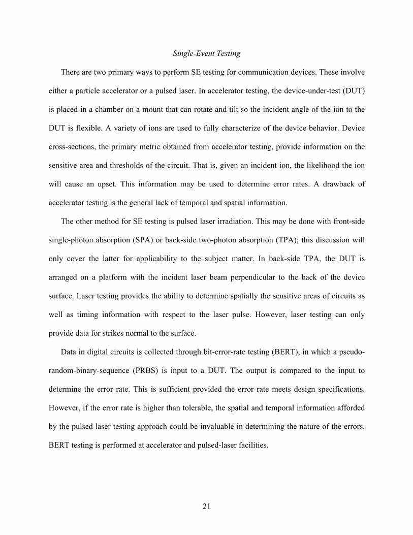
21
Single-Event Testing
There are two primary ways to perform SE testing for communication devices. These involve
either a particle accelerator or a pulsed laser. In accelerator testing, the device-under-test (DUT)
is placed in a chamber on a mount that can rotate and tilt so the incident angle of the ion to the
DUT is flexible. A variety of ions are used to fully characterize of the device behavior. Device
cross-sections, the primary metric obtained from accelerator testing, provide information on the
sensitive area and thresholds of the circuit. That is, given an incident ion, the likelihood the ion
will cause an upset. This information may be used to determine error rates. A drawback of
accelerator testing is the general lack of temporal and spatial information.
The other method for SE testing is pulsed laser irradiation. This may be done with front-side
single-photon absorption (SPA) or back-side two-photon absorption (TPA); this discussion will
only cover the latter for applicability to the subject matter. In back-side TPA, the DUT is
arranged on a platform with the incident laser beam perpendicular to the back of the device
surface. Laser testing provides the ability to determine spatially the sensitive areas of circuits as
well as timing information with respect to the laser pulse. However, laser testing can only
provide data for strikes normal to the surface.
Data in digital circuits is collected through bit-error-rate testing (BERT), in which a pseudo-
random-binary-sequence (PRBS) is input to a DUT. The output is compared to the input to
determine the error rate. This is sufficient provided the error rate meets design specifications.
However, if the error rate is higher than tolerable, the spatial and temporal information afforded
by the pulsed laser testing approach could be invaluable in determining the nature of the errors.
BERT testing is performed at accelerator and pulsed-laser facilities.

22
If temporal information is needed, an oscilloscope is used to record temporal error signatures.
Error characteristics are pre-determined and used as the triggering mechanism for data
collection. This provides good information on a specific type of error, but requires additional
testing if multiple error signatures are to be captured. In a more drastic situation, an
unanticipated error signature could be present and go undetected. Again, this technique is used at
both types of SEE test facilities.
Another data collection technique is frequently used for pulsed-laser SEE testing, but will be
fully described in a later chapter. This technique, called asynchronous data collection, where data
for all error types is collected. In fact, data is collected for each simulated strike because the
oscilloscope is triggered by the laser pulse. Asynchronous data collection produces a surfeit of
data that requires post-processing, but assures that all error signatures are captured.
Conclusion
This chapter describes the general makeup of a communications device from a systems-
point-of-view. A typical transceiver topology includes the following major parts: a
communications channel, transmitter, and receiver. SerDes devices, a subset of the transceiver
device family, is introduced and established as the primary focus of this dissertation.
The SerDes system can be divided into not only the basic components of the
transmitter/channel/receiver, but also the digital/mixed-signal/analog signal domains, and
data/bias/clock signal groups. The different ways of compartmentalizing the operation of the
system allow for different perspectives on how hardening schemes should be applied.

23
Background information for XAUI, the protocol used in the tested SerDes, is provided to
give an understanding of architecture decisions. Basics of the single-event environment and test
procedures pertinent to this research are also outlined. The following chapter introduces the sub-
circuits of the basic components of SerDes.
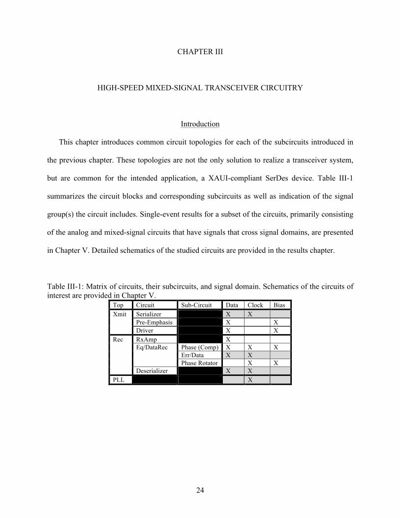
24
CHAPTER III
HIGH-SPEED MIXED-SIGNAL TRANSCEIVER CIRCUITRY
Introduction
This chapter introduces common circuit topologies for each of the subcircuits introduced in
the previous chapter. These topologies are not the only solution to realize a transceiver system,
but are common for the intended application, a XAUI-compliant SerDes device. Table III-1
summarizes the circuit blocks and corresponding subcircuits as well as indication of the signal
group(s) the circuit includes. Single-event results for a subset of the circuits, primarily consisting
of the analog and mixed-signal circuits that have signals that cross signal domains, are presented
in Chapter V. Detailed schematics of the studied circuits are provided in the results chapter.
Table III-1: Matrix of circuits, their subcircuits, and signal domain. Schematics of the circuits of interest are provided in Chapter V.
Top Circuit Sub-Circuit Data Clock Bias Xmit Serializer X X
Pre-Emphasis X X Driver X X
Rec RxAmp X Eq/DataRec Phase (Comp) X X X
Err/Data X X Phase Rotator X X
Deserializer X X PLL X

25
Data Flow Circuitry
Transmitter
Serializer The serializer is a series of precisely-timed 2:1 multiplexors (MUX) in a tree structure that
convert parallel data to serial. Each level of the serializing tree operates at a clock rate divided
down from the transmit data rate in order to bring the serial data to the desired transmission
speed. The number and frequency of incoming bits varies depending on the application but is
limited by the bandwidth of the circuitry. For example, a 4 Gb/s device would require 32-bit data
incoming at 125 Mb/s. This paper will focus primarily on 8b/10b encoded (10-bit) parallel data
incoming at 312.5 MBd to be transmitted at 3.125 GBd1. An example serializer circuit is shown
in Fig. III-1.
After the 8:2 MUX, the encoded data is delivered to the final stage of serializing shift-
registers that furnish the encoded data to the emphasis circuitry. The use of two data lines at this
point allows the use of a half-rate clock to conserve power in the pre-emphasis/equalization stage
by reducing the number of required gates and size of the clock distribution buffers in this stage
[Bu06].
1 An example best explains the difference between (giga) bits-per-second (Gb/s) and (giga)-baud (GBd), symbols-per-second. In 8b/10b
encoded data, 10 encoded bits (symbols) represent 8 bits of data. So, when working with a channel that transmits and receives data at 2.5 Gb/s, such as XAUI, 3.125 x 10⁹ symbols per second (3.125 GBd) must be transmitted, or 10/8 multiplied by the bit rate.

26
Fig. III-1. Diagram of a basic 8-bit serializer circuit. The large dashed box indicates the 8:2 serializer while the small dotted box indicates the clock dividers that provide a quarter-rate and eighth-rate clocks for the serialization logic. Figure from [St08].
Pre-Emphasis
When a signal propagates over a transmission line, the frequency-dependent loss
characteristics of the lane cause amplitude and phase distortion (deterministic jitter) thus
reducing the eye opening of the signal. The amplitude of the high frequency component of the
signal is attenuated, reducing the bandwidth of the signal.
The degradation of the high-frequency component of the signal due to the parasitics of the
transmission line causes inter-symbol interference (ISI). In the case of a single isolated bit
following consecutive identical bits (CIDs), the signal will not have time to completely reach the
state of the isolated bit before another signal is transmitted and may be incorrectly interpreted. In
this way, the current bit depends on the previous bit(s). An example is shown in Fig. III-2.
27
Fig. III-2. Example of a 2.488 Gbps signal showing ISI after transitions (left arrow) and CIDs (right arrow). Note that the first transition after the CID barely crosses the x-axis. Figure from [Max08].
The pre-emphasis circuitry is designed to have a gain that increases with frequency to offset
the frequency-dependent losses in the lane. This shapes the transient signal prior to transmission
to counter the effects of the transmission line and, cascaded with the lane, provides linearity in
the frequency response as demonstrated in Fig. III-3. The magnitude of the pre-emphasis
depends on the characteristics of the transmit medium and may be designed to be adjustable. The
circuitry generally consists of a series of shift registers that provide a timing delay so the value of
the previous bit(s) may be used to determine the value of the current bit. A summing circuit that
combines the weighted output of the shift registers (Fig. III-4) is a typical implementation of a
pre-emphasis circuit. Fig. III-4 depicts a “two-tap” pre-emphasis circuit in which the output
depends on the current and immediate past state. Other possible configurations depend on
multiple past-states and possibly prior states. The cycles in which there is a transition from logic
‘0’ to ‘1’ or logic ‘1’ to ‘0’, are emphasized.

28
Fig. III-3. Example of how equalization (or pre-emphasis) is tuned to cancel ISI. In this example, when the cable and equalizer are cascaded, the signal shows good linearity to 20 GHz. Figure from [Lu08].
Fig. III-4. A pre-emphasis circuit example shows flip-flops as delay generators and differential pairs to execute the emphasis. The feedback element including the loop filter is a simplified PLL, an element described later in this chapter. Figure from [Max08].
An example signal with pre-emphasis is shown in Fig. III-5. In the figure, VO represents the
baseline voltage level and VOP represents the emphasized voltage level. In the case where a data
transition from logic ‘1’ to ‘0’ or ‘0’ to ‘1’ occurs, such as the first identified bit at the left side of

29
the figure, the bit is emphasized because data had transitioned after the previous (unidentified)
bit. However, if there is no transition at the current bit, such as the middle bit (labeled tbit), the
output voltage is at the normal level. The amount of emphasis depends on the expected signal
degradation over the communication channel.
The pre-emphasis circuit simulated for this study is a four-tap device in which the output
depends on the current state as well as the two previous states and the following state.
Fig. III-5. A data series demonstrating the application of pre-emphasis. In the bits following a transition, the signal is emphasized (voltage level is VOP). If there is no transition, the signal is not emphasized (voltage level is VO). Figure from [Max08].
Driver
A standard single-ended line impedance is 50 Ohms. Through Ohm’s Law, if a signal is to be
propagated over this impedance with the circuit biased at 1.2 volts, the current drive in the output
transistors must be a relatively large 24 mA. Most integrated circuit process design kits (PDKs)
include high-voltage thick-oxide devices to act as drivers in the cases where high currents are
necessary. These devices are used in the driver circuitry of the transmitter. In addition to
providing robust output transistors to drive the signal over the lane, the output device impedance
is set at 50-Ohms using precision resistors to match the impedance of the channel. The primary
design challenge of the driver circuitry lays in optimizing power-efficiency.

30
A typical topology of a driver is a differential pair and is often incorporated with the pre-
emphasis circuitry. For example, the differential amplifiers in Fig. III-4 may be implemented
through the thick-oxide devices and the signal transmitted without an additional buffer.
Receiver
Receive Amplifier Upon data receipt, any DC offset is cancelled and the signal is passed through a variable gain
amplifier (VGA) that reduces the signal swing to avoid data clipping to prepare for the
equalization and data recovery blocks. This amplifier must maintain a wide bandwidth.
Otherwise, the time constant, given by 1/(2πf3-dB), will keep the signal from reaching full value.
A common VGA topology is a simple differential pair with a tail-current adjustment for fine-
tuning of the output of the amplifier. The functionality of the VGA is often paired with a peaking
amplifier that provides additional gain and may introduce some signal emphasis prior to the
equalization block. The peaking amplifier may have some external control over the peaking
level.
Equalization/Data Recovery Equalization
In equalization, the weighted outputs of shift registers are summed to reduce ISI in a similar
manner as emphasis in the transmitter. The distinction between equalization and emphasis is that
emphasis adds to the high-frequency components while equalization filters the low-frequency
components of the signal to match the high. In the receiver circuitry, there is the option of a
feedback loop to aid in data decisions, a practice called decision feedback equalization (DFE).
Adjustments to the magnitude of the threshold shift can be made in a pin-selectable configuration

31
that enable or disable h1-hn, gain controls for previously transmitted bits. The simulated CDR
does not include an equalization block. A sample DFE is shown in Fig. III-6.
Fig. III-6. Overview of a DFE architecture. Figure from [Ema07].
Clock and Data Recovery (Data) In most modern SerDes, data is transmitted with clock information embedded in the signal.
This eliminates a separate clock transmission line. The clock and data recovery functional block
is responsible for extracting the embedded clock and using the clock to recover the transmitted
data. CDR circuits are difficult to categorize as specifically related to data or timing systems
because the functionality is directly related to the two signal groups. For the purposes of this
dissertation, the CDR subcircuits are discussed with the timing circuits and introduced later in
this chapter.
Deserializer The deserializer can be realized using shift-registers, demultiplexers (DEMUX) or a
combination of the two. The shift-register topology requires an at-speed clock, which may not be
practical at Gbps speeds. On the other hand, a demultiplexing tree structure requires a clock

32
distribution network, but the highest required frequency is half of the desired bit-rate. The
reduced frequency requirement provides benefits over the shift-register topology in
implementation and power consumption.
Figure III-7 shows a 1:8 DEMUX based on a tree structure. The select pins are connected to
the clock distribution network from the PLL at 1/2, 1/4, and 1/8 rates for SEL0, SEL1, and
SEL2, respectively. A demultiplexing structure is pictured in Fig. III-8.
Fig. III-7. Example of a 1:8 demultiplexing tree structure built from 1:2 DEMUX. The clock distribution network is connected to the select pins. Figure from [To06].
Fig. III-8. A 1:2 DEMUX circuit topology for use in the tree structure in Fig. II-8. Figure from [To06].

33
Timing and Power Circuitry
This section discusses the supporting signal groups: the clock/timing and bias/power circuits.
First, the timing circuits include the serializer and deserializer clock, the phase-locked loop
(PLL), and the clock and data recovery circuit. Discussion centers around the clock and data
recovery and how the clock interacts with the phase rotator and comparator. The bias circuitry
relating to the pre-emphasis, transmit buffer, comparator, and phase rotator are then discussed,
with a focus on designing for low-power operation – an important trait for SerDes used in large
systems with limited power budgets or in portable electronics [Ch07].
Logic Timing and Clock Recovery
Serializer/Deserializer Clock The reference clock for the serializer is typically provided as an external input and is timed at
the baud rate of the circuit (1.6125 GHz). This clock is divided by the number of inputs of the
MUX for each level of serialization. The circuit in Fig. III-1 shows these divide-by clocks.
Similarly for the deserializer, the clock is divided for each level of MUX to provide appropriate
timing to produce the parallel output at the lower data rate. The deserializer in Fig. III-7 indicates
SEL0, SEL1, and SEL2 as clock inputs. These are timed at full-rate, half-rate, and quarter-rate,
respectively. Again, because the serializer and deserializer clock circuits do not cross signal
domains and will not be discussed further in this work.
Phase-Locked Loop
SerDes require precise timing throughout the system provided by the phase-locked loop
(PLL). A block diagram of a typical PLL is shown in Fig. III-9. An off-chip clock operating at a

34
lower-than-data-rate frequency is multiplied by the PLL for clock distribution at-speed or
divided down for timing in specific portions of the system. SerDes designs rely on a PLL in the
transmitter for the divided clocks used in the serializer as seen in Fig. III-1 and also provide the
reference frequency for clock and data recovery in the receiver. The PLL has been identified to
have components sensitive to radiation effects [Bo06], [Lo06]. Due to extensive research for
RHBD PLL design ([Lo06], [Lo07], [Lov07], [Lo08], [Lo09], and [Lov10]), this component is
not discussed in terms of hardening in this document.
Fig. III-9. Block diagram of a basic PLL circuit. Figure from [Be05].
Clock and Data Recovery (Clock)
A clock and data recovery (CDR) circuit has four primary steps: generation of a clock,
comparison of the generated clock to the frequency of the data as detected by the phase detector,

35
correction of the frequency of the generated clock as necessary, and retiming of the input data
with the locked clock frequency. There are several common CDR architectures: injection-locked,
phase-locked, phase-rotating, and fully-digital. Of these, the phase-rotating topology is of
particular interest.
The XAUI interface operates with four lanes operating in parallel. Independent PLLs for
each receiver would come at a large area penalty, particularly for the LC-oscillator PLL topology
– a desired topology due to the speed and accuracy of achieving lock. In this case, a single clock
generator is provided for the XAUI array as shown in Fig. III-10.
The single clock generated for the transmitters in the XAUI array is sufficient because the
serializers are all synchronized with the XGMII structure. However, received data is dependent
on the individual channels and each receiver must have an independent CDR circuit. To ensure
proper timing within each XAUI lane, the clock from the clock generator is rotated to match the
received data through the use of a phase-rotating CDR. The receive-end XGMII resynchronizes
the data after deserialization. A block diagram of a phase-rotating CDR is shown in Fig. III-11.
Fig. III-10. Block diagram of a single PLL clock generator with distributed clock to four transceiver lanes. Figure from [Sa08].

36
In the device topology for simulations discussed in Chapter V, the phase detector block in
Fig. III-11 is implemented as six comparators, which receive data from the receive buffer,
interpret and reconstruct data as a single full-swing digital signal, and identify data error
information to error correcting circuitry. These six devices include one for each of four
quadrature signals as well as early and late signals. For simulation purposes, one comparator is
used to identify SE sensitive devices at the transistor level.
Fig. III-11. Phase-rotating CDR block diagram. Figure from [Sa08].
Bias Circuitry
The bias point of a circuit is critical to proper circuit operation. The current through devices
determines not only the power consumption of the circuit, but also the operating point of each of
the individual transistors. If a circuit is insufficiently biased, a change in carriers in the device,
such as that from a SE, is more likely to change the operating region. The transistor could be
operating in the saturation region and, with a single-event, fall into the ohmic operating region.
On the other hand, an overly-biased circuit contributes to the overall power consumption of the
circuit.

37
Support Circuits
Built-in-Self-Test (BIST)
While it will not be discussed in detail, self-testing circuitry is designed to provide
information for prognostics during the lifecycle of the circuit. This can be done through a
pseudo-random-bit-sequence (PRBS) generator and checker or through a built-in-self-test (BIST)
circuit. The PRBS generator provides a bit pattern that can be used to verify general functionality
via the PRBS checker in the receiver, used for test and characterization of the circuit for off-chip
testing, or for characterization of the lane in a system [St08]. BIST circuitry allows diagnostics to
be delivered directly from the chip and provides a structural test to the user. The BIST testing
generally covers logic operating at relatively low speeds, however, a BIST may be designed to
aid in testing at the system level and needs not to be limited to digital circuitry [Ha02].
Error Detection and Correction (EDAC)
Error detection and correction (EDAC) is an optional function on commercial devices, but
for the mitigation of radiation effects, it is a necessary component. The error detection scheme is
a logic structure traditionally based on Hamming codes [Ha50] that can detect two errors and
correct one. A more involved structure, also based on Hamming codes, can detect three errors
and correct two, but the necessary additional circuitry is quite sizable, in terms of area.

38
Conclusion
This chapter presents a preliminary background on SerDes devices. Additional detail on the
subcircuits of interest will be provided as needed in later chapters. The next chapter presents a
background on single-event phenomena of particular concern to high-speed communication
devices, such as the SerDes, designed for operation in a space environment.
39
CHAPTER IV
SINGLE-EVENT CHARACTERIZATION VIA SIMULATION AND EXPERIMENT
Introduction
Single-event characterization of a circuit typically begins with simulations or, when able,
experiments of the baseline design in which current (or ions/photons) are injected into the circuit,
ideally at each potentially sensitive node, while the output of the circuit is monitored. However,
simply seeing if and how the output “wiggles” as a result of a SE is insufficient to draw any
conclusions about the hardness of the circuit beyond identifying a potential sensitivity. First, the
engineer must collect data that ensures observation of the full range and magnitude of errors. In
simulation, this involves running many individual transistor-level simulations while varying the
simulated LET, the strike time in the data or clock cycle, the incident node, and in some cases,
the relative phase of the clock to the data. In experiment, these variations must be accounted for
during data collection to ensure a full, flexible data set for analysis. Next, error criteria must be
established for the circuit to allow interpretation of the results. After results and error signatures
are collected, the circuit is analyzed for suitability and/or modified to mitigate any sensitivities to
enable further experimental design verification.
This chapter begins with commentary on the identification of error criteria. Next, the SEE
simulation process used throughout this work is described. The two-photon absorption (TPA)
experimental technique is documented after the simulation section. Finally, a technique to
analyze the SE response of a transient circuit through experimental data by establishing the
phase-dependence of SEEs is presented. This technique is called the phase-dependent sensitivity

40
(PDS) technique. These tools, along with heavy-ion testing, provide a means to assess SEE in
circuits from design and simulation to experiment.
Establishing Error Criteria
The understanding of the functionality of a circuit is critical to successful circuit
characterization and analysis. For an individual circuit block that can be simulated at the
transistor level, such as a steady-state operational amplifier, error criteria can be established with
respect to the design specifications of the intended application. However, if the circuit block is
integrated in a larger system, system-wide transistor-level simulations are not always feasible
and macro-models (models that describe circuit behavior through software) will not always
respond accurately to out-of-domain stimuli. A discussion of how the SE error criteria are
determined for the transmitter and receiver follows.
Eye Diagram Masking
The output driver of the transmitter is designed to produce data that conforms to a protocol
standard. As mentioned in Chapter II, an eye diagram is used at the lane to assess signal
performance in terms of jitter and amplitude statistics. For most protocols, an eye diagram
template is provided in the standard to establish error definitions [IEEE08]. The XAUI error
template is shown in Fig. IV-1 with mask values given in Table IV-1.
The resulting transient response of the circuit is analyzed for errors as defined for the
application for each simulated heavy-ion strike. The eye diagram mask is used by virtually
overlaying each bit from the midpoint of the rising edge to the midpoint of the falling edge onto

41
the mask. If any part of the superimposed transient falls within any part of the shaded areas, an
error has occurred.
Fig. IV-1: The XAUI eye diagram template provides a mask to evaluate errors. Any bit from the tested transients that falls within the shaded regions is considered an error. This figure, along with Table IV-1 are used to define error characteristics in subsequent chapters. Figure from [IEEE08].
Table IV-1: Values for XAUI eye-diagram error template in reference to Fig. II-8. UI is the unit interval in seconds and is defined as a bit-width or half of the period of the operating frequency. For XAUI, a UI is nominally 320ps. Symbol Near-End Value Far-End Value Units X1 0.175 0.275 UI X2 0.390 0.400 UI A1 400 100 mV A2 800 800 mV
The transmitter simulations in this work include all analog/mixed-signal subcircuits at the
transistor level. This allows the masking technique to be used to assess errors for strikes
simulated in subcircuit of interest. More details on the simulated subcircuits are found in Chapter
V.
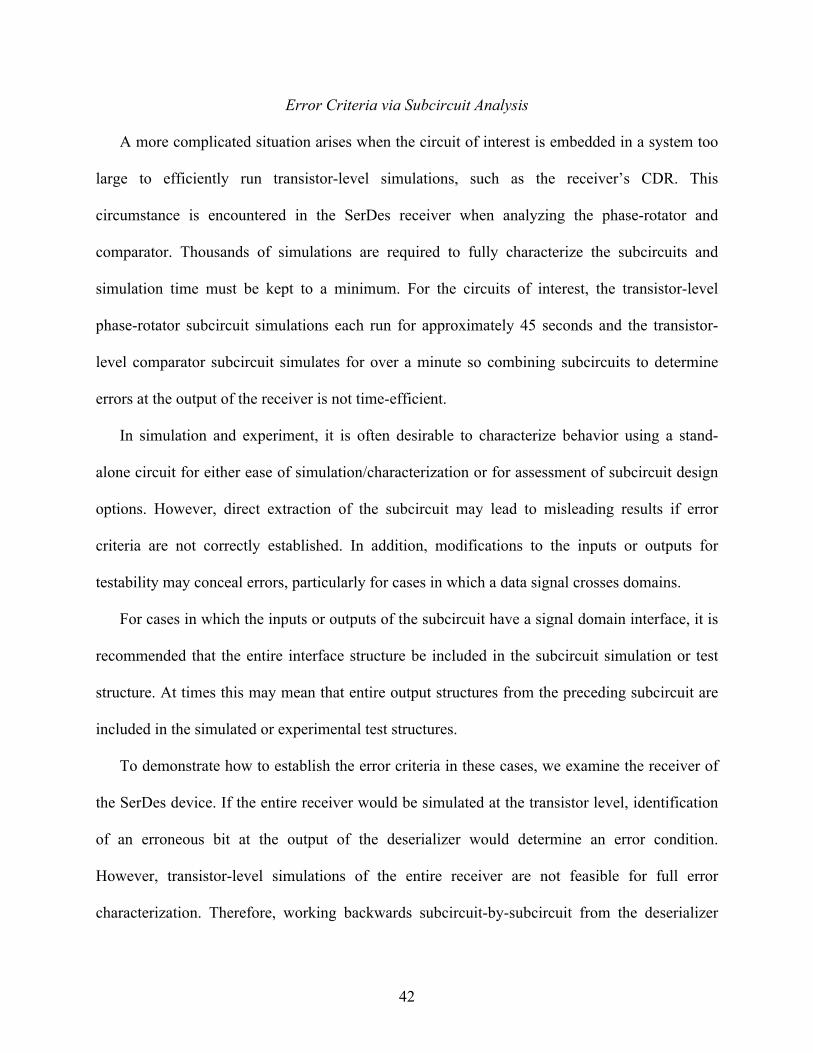
42
Error Criteria via Subcircuit Analysis
A more complicated situation arises when the circuit of interest is embedded in a system too
large to efficiently run transistor-level simulations, such as the receiver’s CDR. This
circumstance is encountered in the SerDes receiver when analyzing the phase-rotator and
comparator. Thousands of simulations are required to fully characterize the subcircuits and
simulation time must be kept to a minimum. For the circuits of interest, the transistor-level
phase-rotator subcircuit simulations each run for approximately 45 seconds and the transistor-
level comparator subcircuit simulates for over a minute so combining subcircuits to determine
errors at the output of the receiver is not time-efficient.
In simulation and experiment, it is often desirable to characterize behavior using a stand-
alone circuit for either ease of simulation/characterization or for assessment of subcircuit design
options. However, direct extraction of the subcircuit may lead to misleading results if error
criteria are not correctly established. In addition, modifications to the inputs or outputs for
testability may conceal errors, particularly for cases in which a data signal crosses domains.
For cases in which the inputs or outputs of the subcircuit have a signal domain interface, it is
recommended that the entire interface structure be included in the subcircuit simulation or test
structure. At times this may mean that entire output structures from the preceding subcircuit are
included in the simulated or experimental test structures.
To demonstrate how to establish the error criteria in these cases, we examine the receiver of
the SerDes device. If the entire receiver would be simulated at the transistor level, identification
of an erroneous bit at the output of the deserializer would determine an error condition.
However, transistor-level simulations of the entire receiver are not feasible for full error
characterization. Therefore, working backwards subcircuit-by-subcircuit from the deserializer
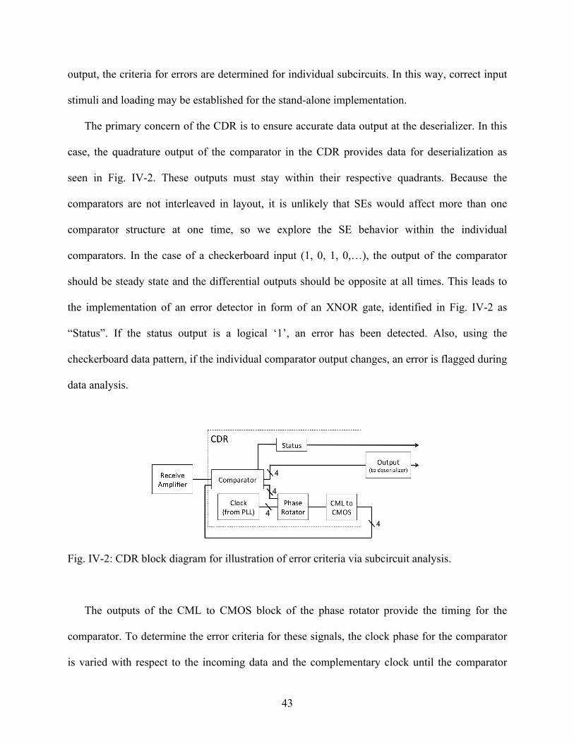
43
output, the criteria for errors are determined for individual subcircuits. In this way, correct input
stimuli and loading may be established for the stand-alone implementation.
The primary concern of the CDR is to ensure accurate data output at the deserializer. In this
case, the quadrature output of the comparator in the CDR provides data for deserialization as
seen in Fig. IV-2. These outputs must stay within their respective quadrants. Because the
comparators are not interleaved in layout, it is unlikely that SEs would affect more than one
comparator structure at one time, so we explore the SE behavior within the individual
comparators. In the case of a checkerboard input (1, 0, 1, 0,…), the output of the comparator
should be steady state and the differential outputs should be opposite at all times. This leads to
the implementation of an error detector in form of an XNOR gate, identified in Fig. IV-2 as
“Status”. If the status output is a logical ‘1’, an error has been detected. Also, using the
checkerboard data pattern, if the individual comparator output changes, an error is flagged during
data analysis.
Fig. IV-2: CDR block diagram for illustration of error criteria via subcircuit analysis.
The outputs of the CML to CMOS block of the phase rotator provide the timing for the
comparator. To determine the error criteria for these signals, the clock phase for the comparator
is varied with respect to the incoming data and the complementary clock until the comparator

44
status flags an error. This error-causing phase shift is used to identify errors at the output of the
phase rotator.
This somewhat tedious procedure must be repeated for circuits preceding the last circuit for
which error criteria have been established. For example, errors at the output of the quadrature
generator at the output of the PLL would be based on the error-causing inputs of the phase
rotator.
As stated earlier, establishing error criteria is essential for accurate SE characterization. It is
possible that error criteria change depending on the circuit’s application and must be carefully
considered prior to data analysis from either simulation or experiment.
Single-Event Simulation
Single-event transient simulations at the transistor level allow the exploration of many
potential scenarios at the low cost of time taken to run the simulator. Assuming correct process
design kit (PDK) models, accurate single-event models are necessary to build confidence in
simulation results. Current-based models have been used for many years to emulate the charge
generated during a SE strike on a device in a circuit. Originally, a double-exponential current
source was used [Ma93], then a technology computer-aided design (TCAD) calibrated model
[Das07] was implemented. More recently, a voltage-dependent current source model has been
developed to accurately simulate the characteristics of an ion strike and an option to simulate
charge-sharing phenomena calibrated to the IBM 90 nm CMOS9SF process [Ka09]. The
voltage-dependent model is the primary SEE model used in this work.

45
Thousands of simulations are run for each circuit to establish sensitive nodes, an estimate of
threshold, and any phase dependence. To simulate the circuit response to a heavy-ion strike, the
voltage-dependent current source is sequentially inserted and simulated in the circuit for every
PMOS and NMOS drain node. Each node is simulated with strikes equivalent to a variety of
LETs. In cases where the signal is periodic, it is necessary to inject the SE throughout the clock
or data cycle to ensure the worst-case strike time is tested. In this work, ten intervals of the clock
or data cycle are simulated for each node and LET. The importance of phase dependence as a
diagnostic tool is discussed in depth later in this chapter.
The outcome of the SEE simulations is a collection of transients that characterize the
behavior of each potentially sensitive node in the circuit over LET and clock (or data) cycle.
Single-Event Laser Experiments
The through-wafer two-photon absorption (TPA) SEU mapping technique, as described in
[McM04], [McM05], and [Lov07], is used to perform SET upset mapping of the circuit and
characterize the transient response. The TPA SEE experimental setup is described in detail in
[McM02] and [McM03]. For this work, TPA laser experiments are performed at the Naval
Research Laboratory Laser Facility. At this facility, the device under test (DUT) is mounted on a
motorized xyz translation platform with 0.1 µm resolution. Optical pulses are focused through the
exposed back side of the wafer onto the active areas of the DUT with a 100x microscope
objective, resulting in a near-Gaussian beam profile with a typical diameter of approximately 1.6
µm at focus [McM03]. Because the carrier deposition varies as the square of the irradiance
[Bog86], [McM02], and [McM03], this corresponds to a Gaussian carrier density distribution

46
with an approximate diameter of 1.1 µm (full-width-at-half-maximum). All experiments are
performed at room temperature. Details of platform resolution and effective spot size may vary
from facility to facility.
Prior to executing a scan of the topology, areas are analyzed for a laser pulse energy
threshold, defined as the lowest pulse energy for which a perturbation of the output is
observable. For experiments presented in this dissertation, the threshold is determined by
visually monitoring the output transients on the oscilloscope as the pulse energy and position are
adjusted.
The surface of each circuit block of interest is scanned using an automated data collection
setup that controls the x-y position of the device and captures data from the oscilloscope with
little interaction from the operator. For each step in the scan, data are recorded using an
oscilloscope, field-programmable gate array (FPGA), or other monitoring device.
In experiments for this work, an oscilloscope is operated in “fast-frame” mode such that each
x-y location in the scan generates a number of individual transients resulting from multiple
triggered events.
In these experiments, the oscilloscope is triggered off the laser pulse, as opposed to standard
practices (typical heavy-ion testing, for example) in which the oscilloscope is triggered off the
upset event itself, using a set threshold and some distinguishing characteristic behavior of the
transient events. Triggering off the laser ensures that events are recorded for each x-y position of
the scan, and that the events occur with a well-defined temporal relationship to the trigger
source, that is, the delay between the laser trigger signal and the laser strike on the DUT is
known. This approach provides insights into unexpected circuit behavior, such as a novel error
response that may not be captured using a preset triggering scheme.
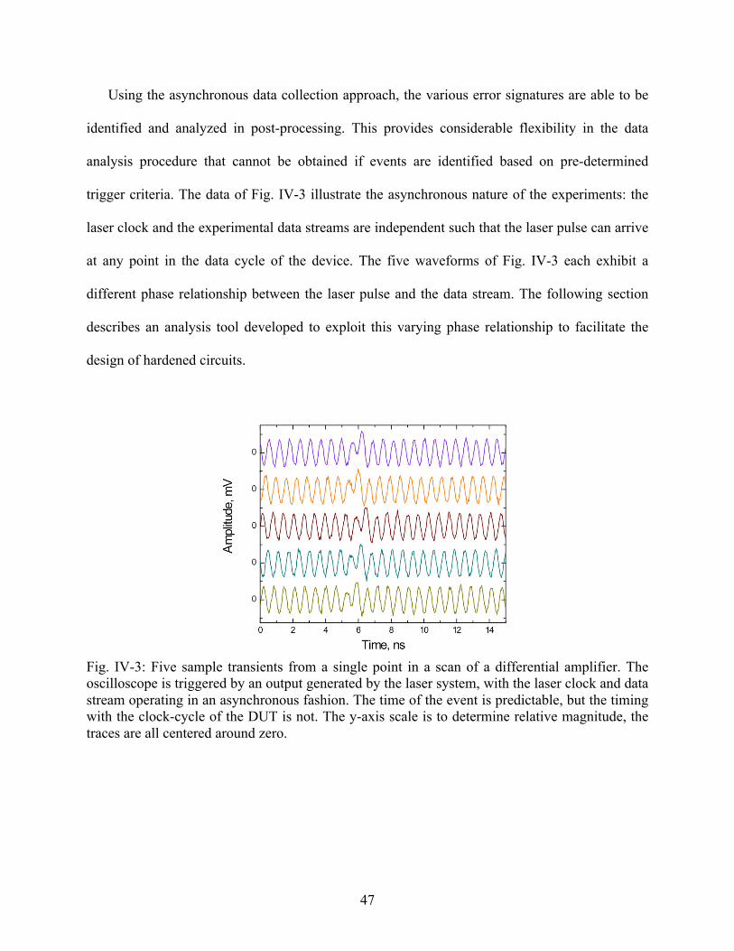
47
Using the asynchronous data collection approach, the various error signatures are able to be
identified and analyzed in post-processing. This provides considerable flexibility in the data
analysis procedure that cannot be obtained if events are identified based on pre-determined
trigger criteria. The data of Fig. IV-3 illustrate the asynchronous nature of the experiments: the
laser clock and the experimental data streams are independent such that the laser pulse can arrive
at any point in the data cycle of the device. The five waveforms of Fig. IV-3 each exhibit a
different phase relationship between the laser pulse and the data stream. The following section
describes an analysis tool developed to exploit this varying phase relationship to facilitate the
design of hardened circuits.
Fig. IV-3: Five sample transients from a single point in a scan of a differential amplifier. The oscilloscope is triggered by an output generated by the laser system, with the laser clock and data stream operating in an asynchronous fashion. The time of the event is predictable, but the timing with the clock-cycle of the DUT is not. The y-axis scale is to determine relative magnitude, the traces are all centered around zero.
48
Analysis Tools Derived from Simulation and Experiment
Data collection with completeness of response in mind results in the production of very large
data sets. These data allow the analysis of atypical or unexpected circuit response without
additional testing. In addition, the response of the circuit in with respect to strikes on a sensitive
node can be fully characterized using the collected data, providing an analysis tool for designers
allowing focused hardening of subsequent circuit designs.
It is well understood that single-event transients (SETs) in combinational logic are captured
(latched) only when the SET arrives during some fraction of a clock cycle (near the clock edge).
This sensitive time period is referred to as the window of vulnerability (WOV), and varies with
the clock frequency and the charge generated by the ionizing event [Bu93]. Determining the
window of vulnerability in an experimental setting is difficult, especially for circuits operating at
high frequencies. The WOV parameter is rarely measured experimentally due to the complexity
of synchronizing the circuit clock with a repetitive ionizing event. This measurement is
especially difficult in broadbeam accelerator experiments.
When referring to analog circuitry, WOV is a misnomer because the sensitivity of the circuit
is measured with respect to the phase of the data cycle as opposed to time in relation to the clock.
In this work, the vulnerability of the device is described as the phase-dependent sensitivity
(PDS). The WOV nomenclature is used only when referring to digital circuitry or referencing
previous works that use the acronym. PDS is used throughout to reference sensitivities in analog,
mixed-signal, as well as digital circuits.
We take advantage of the intrinsic asynchronous nature of laser-induced SEE experimental
approaches and demonstrate a new method for experimentally extracting the phase sensitivity of

49
a circuit. The results presented here illustrate the utilization of the time-domain via the laser data
collection technique described in the previous section. The intrinsic asynchronous characteristic
of the experimental setup allows an examination of phase-dependent circuit behavior to extract
the PDS, eliminating the complexities associated with synchronizing the circuit to the
experiment. Detailed characterization of the parameter space that affects the PDS in high-speed
circuits is made possible and the analysis provides a tool to improve future RHBD circuit
designs.
Previous work describes a technique for determining the WOV in combinational logic via a
pulsed laser synchronized with the circuit clock [Bu93] and determining the WOV through a
simulation technique [Kau04]. The experimental technique is not widely used because of the
complexities in matching the circuit clock to the laser operating frequency, particularly in
today’s high-speed circuits. As a case in point, in most picosecond and femtosecond laser
systems, the laser pulse repetition rate is synchronized to a master oscillator and, therefore, is not
tunable. In such cases, synchronization with the operating frequency of the circuit is difficult or
impossible. Asynchronous laser test results have previous been used to mathematically determine
the WOV [Buc95]. The technique described in this section is derived from this procedure.
SEE simulations are extensively used and can be valuable in determining the WOV.
However, they cannot provide the confidence achieved through experimental characterization.
An example of a simulated WOV diagram for a system is shown in Fig. IV-4. The top frame
denotes the source of upsets and errors in a combinational logic circuit, the number of sensitive
nodes for each error type, and the time period within a conversion cycle (shown in the bottom
frame) in which the vulnerable nodes are sensitive to SEEs. This figure illustrates the complex

50
nature of the WOV in modern circuits and implies the difficulty in experimentally extracting
such detailed information, thus motivating this work.
Fig. IV-4: Example of a simulated system WOV. The bottom figure shows the conversion cycle for a system. The top figure shows the source of errors or upsets, the number of nodes that elicit that response, and the duration with respect to the conversion cycle for which the error is likely. The proposed technique will enable an easy method to experimentally extract similar information from high-speed devices. Figure from [Kau04]1.
A data analysis program determines the elapsed time between the rising edge of the data and
the laser strike of each signal stream (Fig. IV-5). Another way to visualize the outcome of this
process in seen in Fig. IV-6 in which the rising edge of the data cycles have been aligned and the
times of the corresponding laser strikes are identified by vertical lines. The extracted Δt values of
each transient are converted to a phase value (between 0 and 2π) and binned in a histogram to
ensure sufficient data are collected to have a uniform distribution of laser strikes across the data
1 The acronym ‘TNH’ in the top panel of the figure stands for track-and-hold, referencing a subcircuit in the simulated system.
!

51
cycle. This metric is demonstrated with the histogram of pre-emphasis circuit data to be
described in Chapter V (Fig. IV-7).
Fig. IV-5: Schematic diagram illustrating the process for determining the strike time in the clock cycle. The time difference between the zero crossing (left vertical line) and the laser strike time (right vertical line) defines the phase relationship of each trace relative to the error injection and is determined by a computer scripted process.
Fig. IV-6: Three traces lined up in phase to directly illustrate the difference in response with laser strikes at different times in the data cycle. The vertical lines indicate the time of the laser strike for each individual trace. The times between the aligned zero crossing and the respective strike are collected for further analysis.

52
Fig. IV-7: Distribution of strike times over the data cycle. Taken from a TPA test of the 6 dB pre-amplifier circuit shown in Fig. V-3.
During data analysis, errors are processed based on the characteristics observed during the
testing process using thresholds determined by the constraints of the application. In the example
situation, the script checks for bits that do not meet a user-defined voltage threshold criterion
(see shaded region of Fig. IV-5). In the case of a PLL circuit, errors are identified as shifts in the
frequency of the clock [Lo06]. When errors are identified, the corresponding Δt values are
binned as described for Fig. IV-7. The resulting histogram identifies the phase(s) of the data
cycle for which the laser irradiation produced errors, thus providing the PDS.
PDS Example
To illustrate the PDS extraction process, data from a 3.5 nJ TPA scan of a PLL circuit
(designed using the IBM 130 nm CMRF8SF process and not associated with the design used
elsewhere in this work) are analyzed for single-event-induced jitter response and identified errors
are binned with respect to the strike time in the 150 MHz data cycle. Previous works have
indicated the extreme single-event vulnerability of the charge pump sub-circuit with respect to
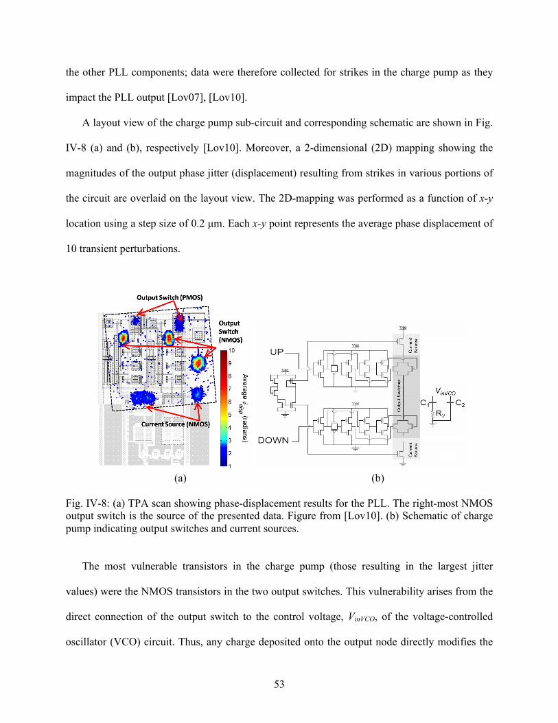
53
the other PLL components; data were therefore collected for strikes in the charge pump as they
impact the PLL output [Lov07], [Lov10].
A layout view of the charge pump sub-circuit and corresponding schematic are shown in Fig.
IV-8 (a) and (b), respectively [Lov10]. Moreover, a 2-dimensional (2D) mapping showing the
magnitudes of the output phase jitter (displacement) resulting from strikes in various portions of
the circuit are overlaid on the layout view. The 2D-mapping was performed as a function of x-y
location using a step size of 0.2 µm. Each x-y point represents the average phase displacement of
10 transient perturbations.
(a) (b)
Fig. IV-8: (a) TPA scan showing phase-displacement results for the PLL. The right-most NMOS output switch is the source of the presented data. Figure from [Lov10]. (b) Schematic of charge pump indicating output switches and current sources.
The most vulnerable transistors in the charge pump (those resulting in the largest jitter
values) were the NMOS transistors in the two output switches. This vulnerability arises from the
direct connection of the output switch to the control voltage, VinVCO, of the voltage-controlled
oscillator (VCO) circuit. Thus, any charge deposited onto the output node directly modifies the

54
control voltage and the resulting output frequency of the PLL. Strikes on the PMOS devices also
result in significant phase error, however at less severity due to the high frequency limitations in
the bandwidth of the PLL. Strikes on the PMOS devices increase the instantaneous output
frequency, whereas strikes on the NMOS devices lower the instantaneous output frequency
(output frequency can be reduced to approximately 0 Hz) [Lov10]. The pull-up (PMOS) and
pull-down (NMOS) current sources also result in observable phase jitter, though with less impact
as the output switches filter the response.
The PDS for strikes on the NMOS switches in the charge pump is plotted in Fig. IV-9 as the
number of errors with respect to cycle time. Upsets are observable across the entire clock cycle
because the output switches are directly connected to the VCO control voltage. However, errors
tend to be concentrated about the rising and falling edges of the clock cycle, as observed by the
sharp peaks in the distribution. The phase jitter and SE displacement are calculated at the cycle
edges, therefore, strikes timed to the clock edges result in a more immediate shift in the output
frequency of the VCO. Strikes timed to the center of the clock cycle will also result in an
apparent stretching or compressing of the output signal, however will be slightly damped due to
the delayed effect until the next observable clock edge.

55
Fig. IV-9: Number of errors with respect to cycle time for NMOS switches in a PLL. Note that the number of errors correlates to the rising and falling edges in the overlaid data cycle.
Conclusions
This chapter presents a set of tools that, along with heavy-ion testing, can identify and
describe SEE in circuits. The process involves defining errors, running simulations and
performing experiments to fully characterize the errors over potentially sensitive nodes, LET,
and through the clock cycle. These techniques are referenced throughout the rest of this work.
The establishment of subcircuit division for either simulation or experiment is crucial to
avoid oversight in SEE characterization. Signal domain interfaces should not be divided over two
subcircuits. These interfaces should also be included in full on breakout test structures.
The TPA laser technique recommends collection of multiple transients while the circuit is
operating asynchronously with the trigger signal. The lack of a phase relationship between the
laser and the circuit results in error injection at random points in the cycle, permitting a complete
mapping of the error susceptibility throughout the data (clock) cycle of the circuit. This
technique provides enhanced understanding of the SET response of the device.

56
The PDS visualizations of the data allow the designer to more fully understand the behavior
of the circuit by providing a point of reference for the likelihood that an error will occur relative
to the timing of the circuit. This, along with knowledge of the circuit state at the time of errors,
helps identify the mechanism causing the error and leads to targeted design improvements. In
addition, the analysis technique can be used to determine the vulnerable percentage of the data
cycle, which can be used to aid in the estimation of the error rate. With careful planning, this
flexible data set and analysis technique can reduce the amount of time required for circuit
iteration. The ease in the experimental determination of the phase-dependence of the circuit
demonstrated here illustrates the intrinsic advantages of the time-domain laser SEE approaches
developed previously [Ar09], and should enable this metric to be more widely utilized in the
future.

57
CHAPTER V
SINGLE-EVENT CHARACTERIZATION OF SELECT SERDES SUBCIRCUITS
Introduction
As stated in Chapter III, the full-swing digital circuits are not discussed in this paper due to
the rich literature base focused on SE RHBD of combinational and sequential digital circuits.
This chapter highlights the simulation results of the circuits of interest: the output of the
transmitter and the mixed-signal portions of the CDR. These circuits are noted in Table V-1.
The presented results are gathered using the techniques described in Chapter IV via
simulation and, when possible, experiment of the subcircuits of a SerDes designed by Boeing in
the IBM 90 nm CMOS9SF process, unless otherwise noted.
Table V-1: List of simulated circuits. Top Circuit Sub-Circuit Data Clock Bias Simulated? Xmit Serializer X X N
Pre-Emphasis X X Y Driver X X Y
Rec RxAmp X Y Eq/DataRec Phase (Comp) X X X Y
Err/Data X X N Phase Rotator X X Y
Deserializer X X N PLL X N

58
Transmitter Circuits
The simulated and tested transmitter driver was designed as a differential current-mode
amplifier with resistor loads to provide extended attachment unit interface (XAUI)-compliant
low voltage differential signals (LVDS) [IEEE08] to the communications channel. Within this
circuit block are pre-driver gain stages in 1, 3, and 6 dB steps used to implement signal pre-
emphasis for improved far-end signal integrity [Zha02]. A block diagram of the transmitter
driver is shown in Fig. V-1.
Fig V-1: Block diagram of transmitter driver. The level shifter / pre-amp combinations provide equalization to the signal and prepare the data to conform to a selected transmission protocol.
Typical design metrics of the output of a transmitter include period jitter and data throughput.
Of particular interest is the response of the basic circuit blocks to single-event perturbations,
which can manifest as unintended pulse transients, additional jitter above the pre-rad baseline,
and signal distortion. The high current drive of the transmitter driver requires the use of high-
voltage thick-oxide devices, which are instantiated as annular devices.
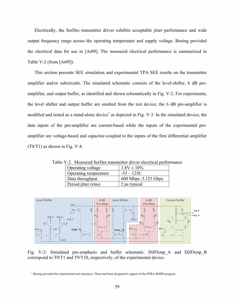
59
Electrically, the SerDes transmitter driver exhibits acceptable jitter performance and wide
output frequency range across the operating temperature and supply voltage. Boeing provided
the electrical data for use in [Ar09]. The measured electrical performance is summarized in
Table V-2 (from [Ar09]).
This section presents SEE simulation and experimental TPA SEE results on the transmitter
amplifier and/or subcircuits. The simulated schematic consists of the level-shifter, 6 dB pre-
amplifier, and output buffer, as identified and shown schematically in Fig. V-2. For experiments,
the level shifter and output buffer are omitted from the test device; the 6 dB pre-amplifier is
modified and tested as a stand-alone device1 as depicted in Fig. V-3. In the simulated device, the
data inputs of the pre-amplifier are current-based while the inputs of the experimental pre-
amplifier are voltage-based and capacitor-coupled to the inputs of the first differential amplifier
(T0/T1) as shown in Fig. V-4.
Table V-2. Measured SerDes transmitter driver electrical performance
Operating voltage 1.8V ± 10% Operating temperature -55 – 125C Data throughput 600 Mbps–3.125 Gbps Period jitter (rms) 2 ps typical
Fig. V-2: Simulated pre-emphasis and buffer schematic. DiffAmp_A and DiffAmp_B correspond to T0/T1 and T9/T10, respectively, of the experimental device.
1 Boeing provided the experimental test structures. These had been designed in support of the DTRA RHBD program.

60
Fig. V-3: Simplified 6 dB pre-amp used in experiments. T0/T1 and T9/T10 are the differential amplifiers, T2/T3 is the output stage, and the current mirror includes each of the transistors at the bottom of the figure. The current drive increases from left to right on the schematic. Unlike the simulated device, the bias point is set off-chip.
Fig. V-4: Different input structures used in simulation (left) and experiment (right). The input data are current based in the simulation version and voltage based in the experimental version.
Transmitter Simulation Results
The voltage-dependent BSIM4 model, noted in Chapter IV, is calibrated to the 90 nm design
process used in this design [Ka09] and accurately reflects the resultant single-event pulse shape.
The most sensitive regions of the simulated transmitter amplifier device are found to be the
transistors in the level-shifting differential inputs to the 6 dB pre-amplifier at the interface of the
level-shifter to the pre-amplifier (see Fig. V-2). These nodes are the current-mode data devices of

61
the pre-amplifier, and a strike disrupts the current supply for the amplifier and therefore disrupts
the data. During a strike, circuit current is reduced through the estimated collection duration
increasing the delay of the output during a single period (Fig. V-5). At the simulated 3.125 Gb/s
throughputs, a PMOS-strike decreases the observed output bit period for only one clock cycle
(two bits). During this time the circuit exhibits an underdamped response with limited overshoot
and phase displacement for the proceeding clock cycle. Figure V-5 shows an example simulation
result for a 153 fC strike to the PMOS input node of the 6 dB pre-amplifier illustrating two
disrupted bits for this type of error.
Fig. V-5: Typical bit error from simulation for a PMOS-strike on the 6 dB pre-amp input node. It can be seen that the struck transient (solid red line) deviates from the expected transient (dashed black line) and causes a significant difference (±20% change) in the bit period. Simulation is run at 1.56 Gb/s.
Figure V-6 shows a graph of the maximum phase displacement due to strikes to the drain of
the NMOS transistors connected to the Data_N and Data_P nodes during a simulation of the
circuit operating at 3.125 Gb/s. Phase displacements over 0.125π radians are considered errors.
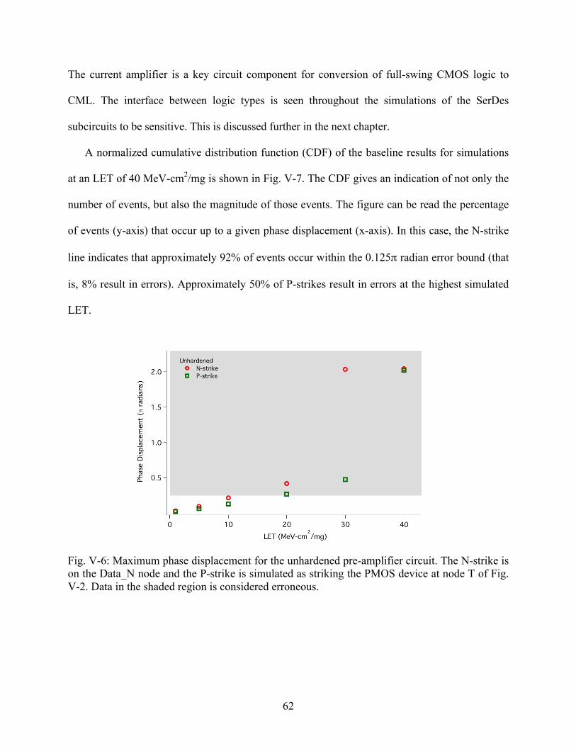
62
The current amplifier is a key circuit component for conversion of full-swing CMOS logic to
CML. The interface between logic types is seen throughout the simulations of the SerDes
subcircuits to be sensitive. This is discussed further in the next chapter.
A normalized cumulative distribution function (CDF) of the baseline results for simulations
at an LET of 40 MeV-cm2/mg is shown in Fig. V-7. The CDF gives an indication of not only the
number of events, but also the magnitude of those events. The figure can be read the percentage
of events (y-axis) that occur up to a given phase displacement (x-axis). In this case, the N-strike
line indicates that approximately 92% of events occur within the 0.125π radian error bound (that
is, 8% result in errors). Approximately 50% of P-strikes result in errors at the highest simulated
LET.
Fig. V-6: Maximum phase displacement for the unhardened pre-amplifier circuit. The N-strike is on the Data_N node and the P-strike is simulated as striking the PMOS device at node T of Fig. V-2. Data in the shaded region is considered erroneous.
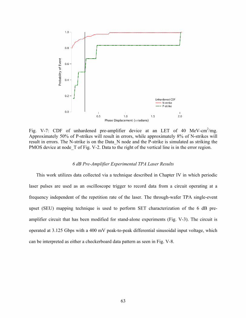
63
Fig. V-7: CDF of unhardened pre-amplifier device at an LET of 40 MeV-cm2/mg. Approximately 50% of P-strikes will result in errors, while approximately 8% of N-strikes will result in errors. The N-strike is on the Data_N node and the P-strike is simulated as striking the PMOS device at node_T of Fig. V-2. Data to the right of the vertical line is in the error region.
6 dB Pre-Amplifier Experimental TPA Laser Results
This work utilizes data collected via a technique described in Chapter IV in which periodic
laser pulses are used as an oscilloscope trigger to record data from a circuit operating at a
frequency independent of the repetition rate of the laser. The through-wafer TPA single-event
upset (SEU) mapping technique is used to perform SET characterization of the 6 dB pre-
amplifier circuit that has been modified for stand-alone experiments (Fig. V-3). The circuit is
operated at 3.125 Gbps with a 400 mV peak-to-peak differential sinusoidal input voltage, which
can be interpreted as either a checkerboard data pattern as seen in Fig. V-8.
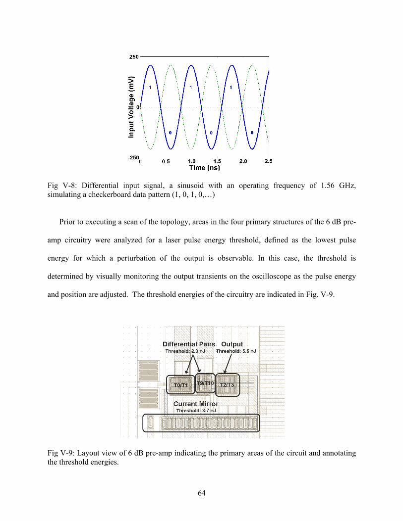
64
Fig V-8: Differential input signal, a sinusoid with an operating frequency of 1.56 GHz, simulating a checkerboard data pattern (1, 0, 1, 0,…)
Prior to executing a scan of the topology, areas in the four primary structures of the 6 dB pre-
amp circuitry were analyzed for a laser pulse energy threshold, defined as the lowest pulse
energy for which a perturbation of the output is observable. In this case, the threshold is
determined by visually monitoring the output transients on the oscilloscope as the pulse energy
and position are adjusted. The threshold energies of the circuitry are indicated in Fig. V-9.
Fig V-9: Layout view of 6 dB pre-amp indicating the primary areas of the circuit and annotating the threshold energies.

65
To observe the effects of SEE, a laser is scanned across the T9/T10 differential amplifier
(Fig. V-9) in 0.3 µm steps at an incident laser pulse energy of 6.9 nJ – sufficiently above
threshold to produce SETs without saturating the error response. An automated data collection
setup controls the x-y position of the device and captures data from the oscilloscope with little
interaction from the operator. For each step in the scan, multiple transients triggered off the
repeating laser strikes are recorded using a Tektronix 12 GHz TDS6124 oscilloscope operating
with a resolution of 20 GS/s. For each transient event, data points are recorded with adequate
oscilloscope resolution at the time of the laser strike to allow accurate analysis.
The laser experimental results demonstrate a different type of SEE errors than those observed
in simulation. Collected data are analyzed for phase errors using the same criteria as described in
Chapter IV. Initial data analysis does not reveal any phase errors. This result is not surprising due
to the differences in the inputs to the simulated and experimental circuits – the most sensitive
node is not represented in the experimental circuit. Bit errors are observed during testing and the
data post-analysis was expanded to include testing for this error type. The bit error occurs when a
bit maximum or minimum does not reach the threshold necessary for the logic to switch from a
‘0’ to a ‘1’, or vice-versa, and will result in misread data (Fig. V-10). In extreme cases, more
than one successive bit may be upset resulting in multiple-bit upsets (MBU). No MBUs were
observed in these experiments, however, presumably an indication of success in the RHBD
approaches utilized. A representative transient illustrating a bit error is shown in Fig. V-11.

66
Fig. V-10: Illustration of bit error. An error occurs if the measured voltage level does not reach a percentage of the expected voltage level. This percentage is considered the error threshold.
A summary of number of upsets observed in each area of the circuit is given in Table V-3.
These results indicate that the T9/T10 differential amplifier is the most sensitive circuit element
tested. This result is somewhat surprising since the currents driving this device are greater than
those in T0/T1, and increasing the current drive is a standard way of mitigating SETs in circuits.
The transistor sizes in T9/T10 are the same as those in T0/T1, and bias conditions put T9/T10
operating closer to the ohmic / saturation boundary; thus a smaller change in the current, ID, is
required to affect the output of the circuit, in this case due to the charge injected by the laser
pulse. It is expected that lowering the bias current through T5 (see Fig. V-3) or reducing the
collector resistor values of T9/T10 would increase VDS such that both transistors would operate
well into the saturation region and would require a larger injected charge to disrupt operation
than in the current configuration.

67
Fig. V-11. Sample transient for a bit upset in T0/T1 resulting from a laser pulse energy of 6.9 nJ. This is a typical example of the observed bit upsets throughout the circuit. The shaded region indicates the areas in which an error is identified. In this case, the error threshold is 50% of the average peak voltage.
Table V-3: Summary of number of upsets observed by circuit area. 6.9 nJ laser pulse energy. Missed Bits T0/T1 339 T9/T10 3001 T2/T3 0 CM 0
The ability to analyze the data in post-processing as is done here leads to considerable
flexibility and is an intrinsic strength of the present approach. To further illustrate this point
additional experiments were performed on T9/T10 as a function of the laser pulse energy (3.2 nJ
and 4.6 nJ). The test setup is identical to that of the original data except that five transients are
recorded for each x-y position in the scan and a higher resolution (0.3 mm) step size is used.
Figure V-12 shows bit error maps for T9/T10 at two laser pulse energies; the transistor
structure is clearly defined in the examples. No errors are detected at two lower pulse energies
even though a visual perturbation of the signal was observed during testing.
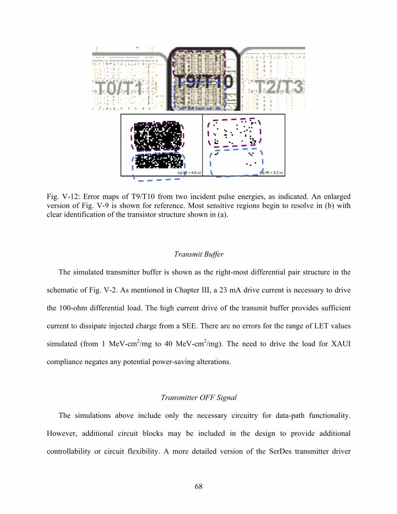
68
Fig. V-12: Error maps of T9/T10 from two incident pulse energies, as indicated. An enlarged version of Fig. V-9 is shown for reference. Most sensitive regions begin to resolve in (b) with clear identification of the transistor structure shown in (a).
Transmit Buffer
The simulated transmitter buffer is shown as the right-most differential pair structure in the
schematic of Fig. V-2. As mentioned in Chapter III, a 23 mA drive current is necessary to drive
the 100-ohm differential load. The high current drive of the transmit buffer provides sufficient
current to dissipate injected charge from a SEE. There are no errors for the range of LET values
simulated (from 1 MeV-cm2/mg to 40 MeV-cm2/mg). The need to drive the load for XAUI
compliance negates any potential power-saving alterations.
Transmitter OFF Signal
The simulations above include only the necessary circuitry for data-path functionality.
However, additional circuit blocks may be included in the design to provide additional
controllability or circuit flexibility. A more detailed version of the SerDes transmitter driver

69
circuitry is simulated for select nodes. Again, the circuit is simulated at 3.125 Gbps with a
checkerboard data pattern. A block diagram of the simulated circuitry is shown in Fig. V-13.
In the case of a strike on the OFF circuitry controlling a current DAC in the SerDes output
buffer, charge injected by the models corresponding to an LET of 10 MeV-cm2/mg cause the
circuit to power off. The output diminishes over time until it recovers approximately 25 µs after
the original strike. If a reset signal is sent after the event, the circuit does go back into an
operating state. Figure V-14 shows the differential output transient as observed at the input of the
receiver when a SET with an LET of 10 MeV-cm2/mg strikes. The time scale on the left half of
the graph is extended to show the onset of the event.
The power-down circuitry is not mentioned in the RHBD section because it has a digital
input and events can be mitigated in a number of traditional ways. The purpose of showing this
result is to highlight the potential of error. Regardless of their small die area and low probability
of a single-event strike directly to the power-down device, designers must be cognizant of this
major sensitivity.
Fig. V-13: Block diagram of simulated output structure for a SerDes circuit.

70
Fig. V-14: Differential output transient of simulated SEE strike at the OFF node in Fig. V-10. The circuit recovers at 25 µs
Receiver Circuits
Aside from the deserializer, the receiver’s clocking circuitry is within the clock and data
recovery circuit block. Within the CDR, the comparator and the phase rotator have the mixed-
signal qualities of interest for this dissertation. The CML to CMOS circuit of the phase rotator is
discussed in some depth and results from the CML rotator/mixer are presented. In addition,
findings for the clocked nodes of the comparator circuit are shown at the end of this chapter.
Receiver Buffer
A simplified schematic of the simulated variable gain amplifier (VGA) receive buffer is
shown in Fig. V-15. There are no upsets for the simulated LET range. However, the variable

71
properties do have an effect on the SE response of the circuit. Naturally, when the gain is higher,
events can be more easily dissipated with the increased current. The designer should create the
minimum gain high enough that transients will not cause upsets in the following stage.
Fig. V-15: Schematic of receiver buffer [Bu06].
Clock and Data Recovery
A high-speed communications system with multiple lanes such as a XAUI interface,
typically utilizes a system-wide phase-locked-loop- (PLL) based clock that is distributed to each
of four lanes. The timing of each lane is independent until the signals are recombined after the
data are deserialized. The distributed clock is retimed within the independent lanes to match the
received differential serial data. The in-lane timing is accomplished within the CDR via a
current-mode phase-rotator (see Fig. V-16). The resulting signal is converted to full-swing
CMOS logic in the CML to CMOS circuit block to be fed back to the input of the CDR
comparator.

72
Fig. V-16: Block diagram of a typical receiver and CDR circuit. The CML to CMOS block converts the incoming PLL clock to CMOS logic for use in timing the CDR comparator. All signals are differential.
Phase-Rotator Simulations on the phase-rotator mixer shown in Fig. V-17 yield the maximum phase
displacements shown in Fig. V-18. CDF results are shown in Fig. V-19. The transmission-gate
input nodes, labeled “A”, connect to the first pair of differential amplifiers. These are the most
sensitive nodes in the phase-rotator core circuit. Both N- and P-strikes are simulated at this node
with approximately 10% and 5%, respectively, resulting in errors in the output at 40 MeV-
cm2/mg
The tail currents of the first pair of differential amplifiers (nodes “B”) are derived from the
error signature for the i- and q- quadrature signals at the output of the comparator. These currents
adjust the output phase of the phase-rotator to match the embedded clock from the incoming
data. Only N-strikes are simulated.
The second pair of differential amplifiers, labeled “C”, is also an NMOS-only structure. It
acts as a mixer for the rotated signal. Simulation results for these devices revealed a similar, but
diminished results to the devices at “D” and are omitted for this reason.
The output of the phase rotator, “D” is a current-based clock signal that is converted to a rail-
to-rail clock signal in the CML to CMOS circuit. Both N- and P-strikes are simulated for this
circuit. The connecting device in the CML to CMOS circuit is PMOS (see Fig. V-18).

73
Fig. V-17: Phase rotator schematic
Fig. V-18: Maximum phase displacement for the CML mixer subcircuit of the phase-rotator shown in Fig. V-15. Points in the shaded region are considered errors. The hollow symbols indicates N-strikes, the filled symbol indicates P-strikes.
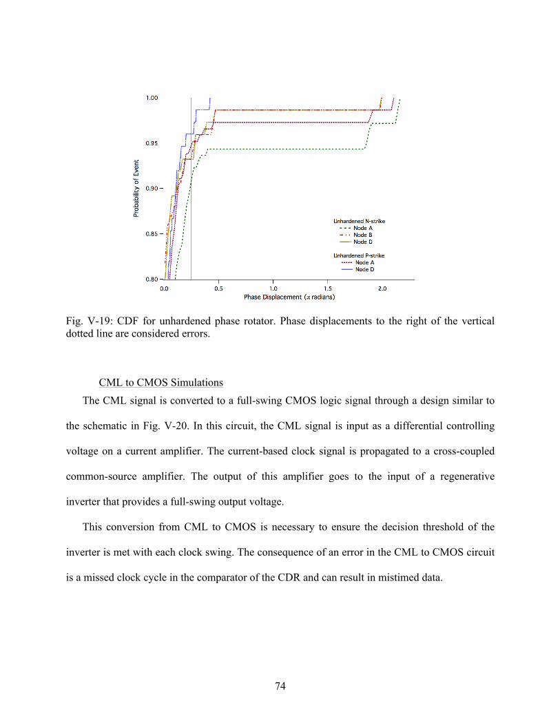
74
Fig. V-19: CDF for unhardened phase rotator. Phase displacements to the right of the vertical dotted line are considered errors.
CML to CMOS Simulations The CML signal is converted to a full-swing CMOS logic signal through a design similar to
the schematic in Fig. V-20. In this circuit, the CML signal is input as a differential controlling
voltage on a current amplifier. The current-based clock signal is propagated to a cross-coupled
common-source amplifier. The output of this amplifier goes to the input of a regenerative
inverter that provides a full-swing output voltage.
This conversion from CML to CMOS is necessary to ensure the decision threshold of the
inverter is met with each clock swing. The consequence of an error in the CML to CMOS circuit
is a missed clock cycle in the comparator of the CDR and can result in mistimed data.
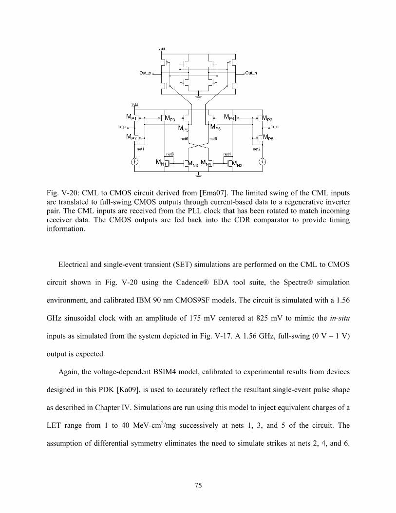
75
Fig. V-20: CML to CMOS circuit derived from [Ema07]. The limited swing of the CML inputs are translated to full-swing CMOS outputs through current-based data to a regenerative inverter pair. The CML inputs are received from the PLL clock that has been rotated to match incoming receiver data. The CMOS outputs are fed back into the CDR comparator to provide timing information.
Electrical and single-event transient (SET) simulations are performed on the CML to CMOS
circuit shown in Fig. V-20 using the Cadence® EDA tool suite, the Spectre® simulation
environment, and calibrated IBM 90 nm CMOS9SF models. The circuit is simulated with a 1.56
GHz sinusoidal clock with an amplitude of 175 mV centered at 825 mV to mimic the in-situ
inputs as simulated from the system depicted in Fig. V-17. A 1.56 GHz, full-swing (0 V – 1 V)
output is expected.
Again, the voltage-dependent BSIM4 model, calibrated to experimental results from devices
designed in this PDK [Ka09], is used to accurately reflect the resultant single-event pulse shape
as described in Chapter IV. Simulations are run using this model to inject equivalent charges of a
LET range from 1 to 40 MeV-cm2/mg successively at nets 1, 3, and 5 of the circuit. The
assumption of differential symmetry eliminates the need to simulate strikes at nets 2, 4, and 6.

76
Finally, to ensure the worst-case scenario is simulated, the SET is injected at varying times in the
clock cycle [Ar11].
To quantify the results, the period of each clock cycle is measured from rising edge to rising
edge and compared with the ideal 640 ps clock period. The variation from the ideal indicates a
temporary shift in clock phase and is referred to as the phase displacement. Errors are identified
as the clock period deviating from the ideal clock value by more than a threshold determined by
the characteristics of the application. In this case, a phase displacement of more than 80 ps
(0.125π radians) is identified as an error. The maximum and average phase-displacement errors
from simulations of the CML to CMOS circuit are shown in Fig. V-21. The most sensitive node,
net1, indicates an error at an LET greater than 5 MeV-cm2/mg and a missed clock bit (phase
displacement greater than π radians) at an LET greater than 10 MeV-cm2/mg. The missed clock
bits recover with the following bit and thus are limited to a value of 2π radians.
A normalized cumulative distribution function (CDF) of the baseline results is shown in Fig.
V-22. The CDF gives an indication of not only the number of events, but also the magnitude of
those events. The figure can be read the percentage of events (y-axis) that occur up to a given
phase displacement (x-axis). In this case, the net1 line indicates that 78% of events occur within
the 0.125π radian error bound (that is, 22% result in errors). Less than 10% of clock cycles from
nets 3 and 5 result in errors.

77
Fig. V-21: Maximum (top) and average (bottom) phase displacement for SE strikes for nets 1, 3, and 5. Results falling above the dashed line are considered errors.
Fig. V-22: Cumulative distribution function of likelihood of magnitude of phase displacement. Events to the right of the vertical line are considered errors.

78
Comparator
A schematic of the data path of the comparator is shown in Fig. V-23. The sensitive nodes
are noted as Data, Latch, and Out. For simulations of the comparator data path, the use of the
XNOR gate as an error flag proved to be non-ideal because of the cross-coupled inverter pair. An
error on one side of the differential signal triggered an error on the other side, typically during
the same clock cycle and therefore no error was detected. Examples of the expected error
triggering and the more common result are shown in Fig. V-24.
Data-path errors are identified by finding state transitions in the output signal rather than the
XNOR status signal. Table V-4 lists the number of simulations that result in errors for each of
three nodes (with the assumption of symmetry).
Fig. V-23: Simulated schematic of comparator. Out_p and Out_n lead to latches that sample the value at the node using the rotated clock. The latched signals are compared with an XNOR gate to indicate an error.

79
Fig. V-24: Illustration of an error captured with the XNOR error signal (top) and an error missed by the XNOR gate (bottom).
Table V-4: Unhardened comparator error count by node and strike-type. Node LET
(MeV-cm2/mg) # Errors
Data 5 0 10 4 20 9 30 17 40 20 Latch 5 6 10 11 20 13 30 16 40 17 Node 5 5 10 9 20 11 30 16 40 16

80
Summary
This chapter introduces the single-event response of the unhardened SerDes subcircuits. The
results suggest three recurring themes: sensitivity in CML, current amplifiers, and when pin-
selectability is used to provide trimming for equalization or for power savings. The upcoming
chapters address each of these concerns by first discussing the primary sensitivities as groups
then applying RHBD techniques in a example case for CML, current amplifiers, and pin-
selectability.

81
CHAPTER VI
COMMON VULNERABILITIES IN SEE RESULTS OF SERDES CHARACTERIZATION
The previous chapter introduces the errors seen in the mixed-signal portions of the SerDes
device. Simulation results reveal three primary vulnerable circuit structures: CML, the interface
between signal types, and within pin-selectable options. This chapter gives a summary of
characteristic errors for the common vulnerabilities and is intended to be a “quick reference” to
each of the scenarios.
The data path, clock, and bias circuitry system are three of the cornerstones of
communications system design. Each of the errors is related to one (or more) of these design
concerns. The CML errors and the signal-type interfaces are associated with the data path and the
clock and the pin-selectable options are associated with the bias circuitry. To more fully describe
the categories, the pre-amplifier and CML to CMOS converter from the phase-rotator are used to
discuss hardening of the CML and interface errors, respectively, in the following chapters.
CML Errors
The sensitivity of the CML circuitry depends strongly on the tail current of the differential
amplifiers. Differences in the experimental and simulation results from the 6 dB pre-amplifier
show this dependence on bias conditions. In addition, simulation of the mixer of the phase
rotator indicates CML sensitivity. Chapter VII develops the SET mitigation strategy for CML

82
circuitry through application of differential charge cancellation (DCC) in both the pre-amplifier
and the phase rotator.
CMOS-CML Interface
A recurring theme of sensitivity in circuits that transition between signal domains is apparent
through the simulation of the SerDes subcircuits. The primary sensitive nodes are found in the
current amplifier structures. These transitions are found in the phase rotator, the pre-amplifier,
and the comparator. Hardening techniques for the CML to CMOS circuit in the phase rotator are
presented in Chapter VIII. DCC shows to be the most effective hardening solution and presents
few design penalties in terms of power, speed, and area. Results for application of DCC to the
current amplifiers in the pre-amplifier and the comparator are also presented in Chapter VIII.
Power and Bias Options
An underlying theme also emerged in discussion of SEE characterization: power
consumption. Under high-current-drive conditions, CML circuits proved to be robust to SETs. It
is up to the designer to balance circuit hardness with power consumption. Due to the high current
draw of CML, designers often provide power-down circuitry for times when the SerDes might be
operating in either a transmit- or receive-only condition. A power-down transistor is found to be
extremely sensitive to SETs.
83
CHAPTER VII
RADIATION-HARDENED-BY-DESIGN TECHNIQUES
Introduction
The concept of radiation-hardened-by-design (RHBD) has become attractive with the
decreased demand for dedicated radiation-hardened fabrication facilities. Rather than relying on
a fabrication process to mitigate errors, designers modify circuits and layouts to best avoid
problems with radiation effects [La03]. Analog and digital circuits require different RHBD
approaches.
The penalties for RHBD techniques for both analog and digital circuitry typically come in the
form of layout area, circuit speed, and power consumption. With the increased awareness of
charge sharing, analog RHBD techniques have used the phenomena to mitigate SETs through
common-mode rejection. The assumption of a high common-mode-rejection-ratio (CMRR)
allows charge generated on neighboring transistors to be canceled. In order to capitalize on the
generated charge, sister devices are placed close together in the layout to promote charge sharing
and use common mode rejection to mitigate the propagating transient [Ke07], [Ar10].
This chapter presents background for digital and analog RHBD techniques. However, the
primary focus of the chapter is differential charge cancellation (DCC) – the primary technique
used in the hardening of CML and domain interface circuitry. Experimental validation of the
concept of the DCC technique is presented.

84
Digital RHBD Techniques
Digital RHBD techniques include charge dissipation techniques and redundancy. Charge
dissipation techniques include the addition of a capacitor, increasing the W/L ratio of the
transistors, and/or adding decoupling resistors or additional transistors to the circuit. These
techniques generally slow the circuit response through the addition of capacitance (a particularly
undesirable effect in high-speed communication devices) and increase area.
Redundancy techniques use copies of information to ensure a correct copy is preserved for
later in the circuit and the concept is succinctly described in Lacoe’s 2003 Short Course notes
[La03]:
SEU hardening by redundant circuit design approaches is based on three fundamental concepts: (1) Information storage redundancy maintains a source of uncorrupted data after an SEU, (2) feedback from the non-corrupted data storage location can cause the corrupted data to recover after a particle strike, and (3) the “intelligence” needed in the feedback to cause recovery of the proper location can be derived from the fact that the current induced by a particle hit flows from n-type diffusion to p-type diffusion.
Triple-modular redundancy (TMR) involves creating three copies of an unhardened logic
block connected to the same clock and data line. The three blocks lead into a voting circuit as
illustrated in Fig. VII-1. This majority voter and assumes that only one copy of the logic will be
struck. The circuitry must be refreshed periodically to ensure that errors are only present for one
clock cycle and do not linger for future voting opportunities [He99]. To enhance the
effectiveness of the concept, designers ensure that the physical layout of the transistors in the
logic blocks were separated such that an ion strike is not likely to affect multiple nodes. The area
penalty of TMR is the primary concern for this SE mitigation technique.

85
Fig. VII-1. Block illustration of TMR (after [Bl02])
Other implementations of redundancy are temporal redundancy [Mav00], spatial redundancy
[Ca96], or a combination thereof [Mav00]. These will not be discussed further in this paper, but
are mentioned here for completeness.
Analog RHBD Techniques
Analog-specific circuit hardening has only recently begun to amass a significant literature
base. Traditional hardening techniques involve increasing the current drive, adding extra
capacitance to a sensitive node, low-pass filters, and redundant circuitry [Lo06]. Recently, dual-
path hardening [Fl08], [Ol08] and techniques that exploit the charge-sharing phenomenon
[Ke07], [Ar10], [Bl10] show promise in the mitigation of single-event transients (SETs) in
analog circuitry. These techniques are outlined in this section.

86
Traditional Analog RHBD Techniques
Traditional analog RHBD techniques include charge dissipation and filtering [La03]. In
charge dissipation, the current drive is increased through key points in the circuit typically by
increasing transistor widths. This provides sufficient drive current to minimize the impact of
generated charge and attenuate SETs. Filtering involves the addition of capacitance to sensitive
nodes to create a low-pass filter that increases the time constant of the node so that the transient
will not propagate to the output. These techniques have primary drawbacks of power
consumption and degraded speed, respectively. In fact, any capacitance added to sensitive nodes
of this circuit degrades the performance of high-speed circuits such that filtering is eliminated as
an RHBD option.
Charge Sharing RHBD Techniques
Reduced spacing requirements in sub-micron technologies have introduced charge-sharing
effects that are detrimental to single-event hardening techniques shown to be effective in larger
(250 nm or greater) processes [Ol05], [Bl05], and [Am06]. This phenomenon, previously
considered a detriment to all circuit operation, is exploited in recently-developed techniques to
mitigate single-event effects (SEE) in fully-differential analog circuits, which have been shown
to be sensitive to single-event transients (SET) [Ste06], [Lo06], and [Fl08].
In previous work, TCAD simulations of a radiation-hardened by design (RHBD) layout
approach were presented using common-centroid transistors in a fully-differential data path to
mitigate the effects of single-events through common-mode rejection with promising results
[Ke07]. This work has been tested experimentally [Ar10] and is described in the next section.

87
The technique has been expanded for use in non-differential circuits such as operational
amplifiers [Bl11] and bias circuitry [Bl10].
Differential Charge Cancellation Experimental results of a RHBD layout technique designed to mitigate SEEs in a 65 nm
technology by exploiting charge-sharing phenomenon in differential circuitry are presented in
this section. The layout technique minimizes the distance between the drains of sister devices in
the differential signal path through matched and common-centroid layouts to maximize the
likelihood of an ion strike affecting both sides of the differential pair, therefore cancelling some,
or all, of the resulting transient. The sensitive area is significantly reduced to standard layouts
that do not promote charge sharing. Results from this study indicate that a practice of layout with
close drain proximity for sister transistors along the fully-differential signal path will greatly
reduce both the sensitive area of the circuit and the amplitude of resulting transients.
The advantages in dynamic output range and noise rejection over single-ended circuits make
differential topologies the accepted standard for high-performance analog design [Am06]. The
sample and hold (S/H) amplifier (Fig. VII-2), has several examples of “sister” devices, i.e.
matched components on different sides of the differential data path. These device pairs feature
two transistors connected such that any differential voltage applied to the inputs is amplified,
making single events (SE) particularly detrimental. However, assuming a large common mode
rejection ratio (CMRR), any common voltage applied to both the inputs is rejected (Fig. VII-3).

88
Fig. VII-2: The S/H amplifier is a commonly used differential switched-capacitor circuit. The dual-data path provides a large dynamic output range and high noise rejection and has several examples of “sister” differential transistors.
For circuits in which device matching is a priority, a common-centroid layout approach is
used in which devices are arranged around a center location so that the effects of process
variation, gradient effects, and random noise are cancelled [Has06]. This is typical in differential
pair inputs, but not necessarily used for other sister devices along a differential signal path such
as switching transistors.
Single-ended analog circuits will be negatively affected by multiple devices collecting
charge. On the other hand, the results of [Ke07] suggest that, in fully-differential A/MS circuits,
the effects of charge sharing may be smaller than that of single-ended circuits if common-mode
rejection properties of sister devices are used. In this case, drains in close proximity and, if
possible, common centroid layouts are expected to minimize the effects of SETs on the circuit.
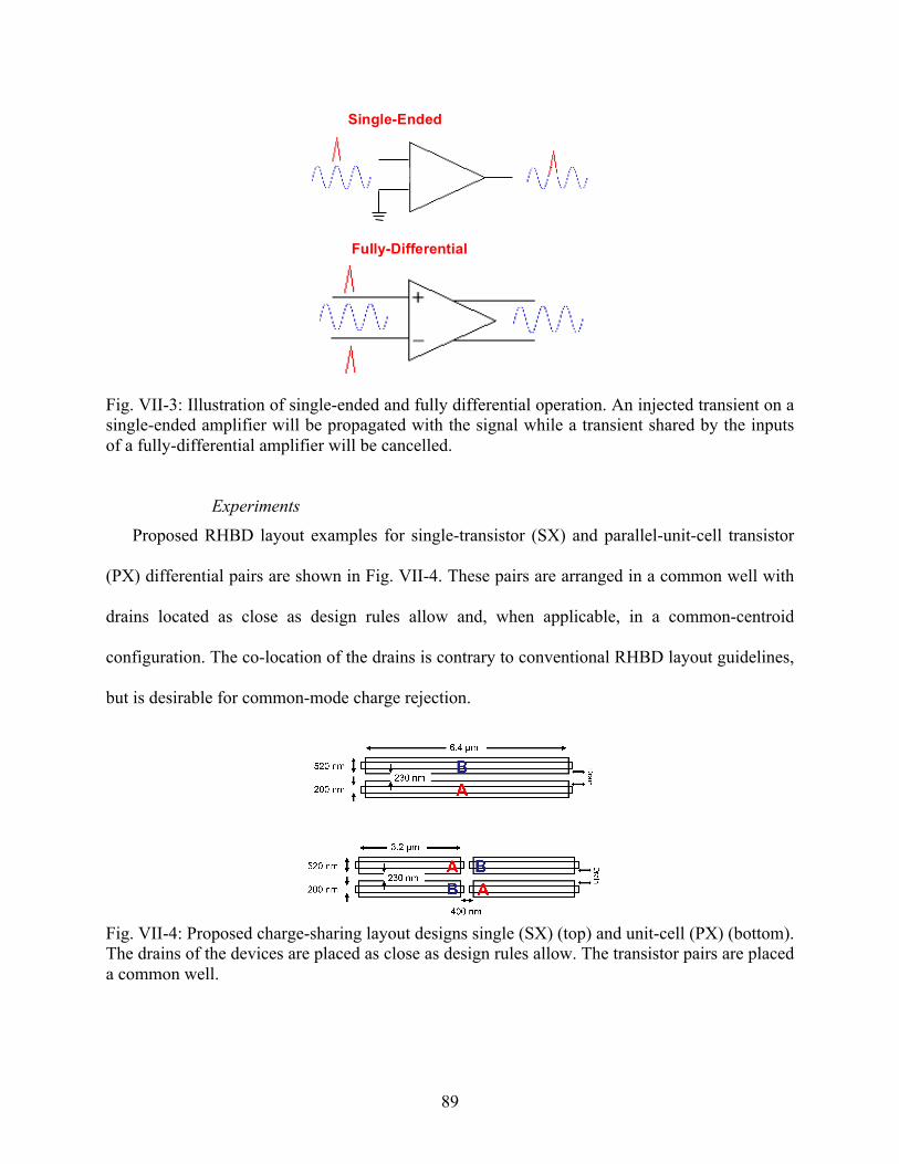
89
Fig. VII-3: Illustration of single-ended and fully differential operation. An injected transient on a single-ended amplifier will be propagated with the signal while a transient shared by the inputs of a fully-differential amplifier will be cancelled.
Experiments Proposed RHBD layout examples for single-transistor (SX) and parallel-unit-cell transistor
(PX) differential pairs are shown in Fig. VII-4. These pairs are arranged in a common well with
drains located as close as design rules allow and, when applicable, in a common-centroid
configuration. The co-location of the drains is contrary to conventional RHBD layout guidelines,
but is desirable for common-mode charge rejection.
Fig. VII-4: Proposed charge-sharing layout designs single (SX) (top) and unit-cell (PX) (bottom). The drains of the devices are placed as close as design rules allow. The transistor pairs are placed a common well.
Single-Ended
Fully-Differential
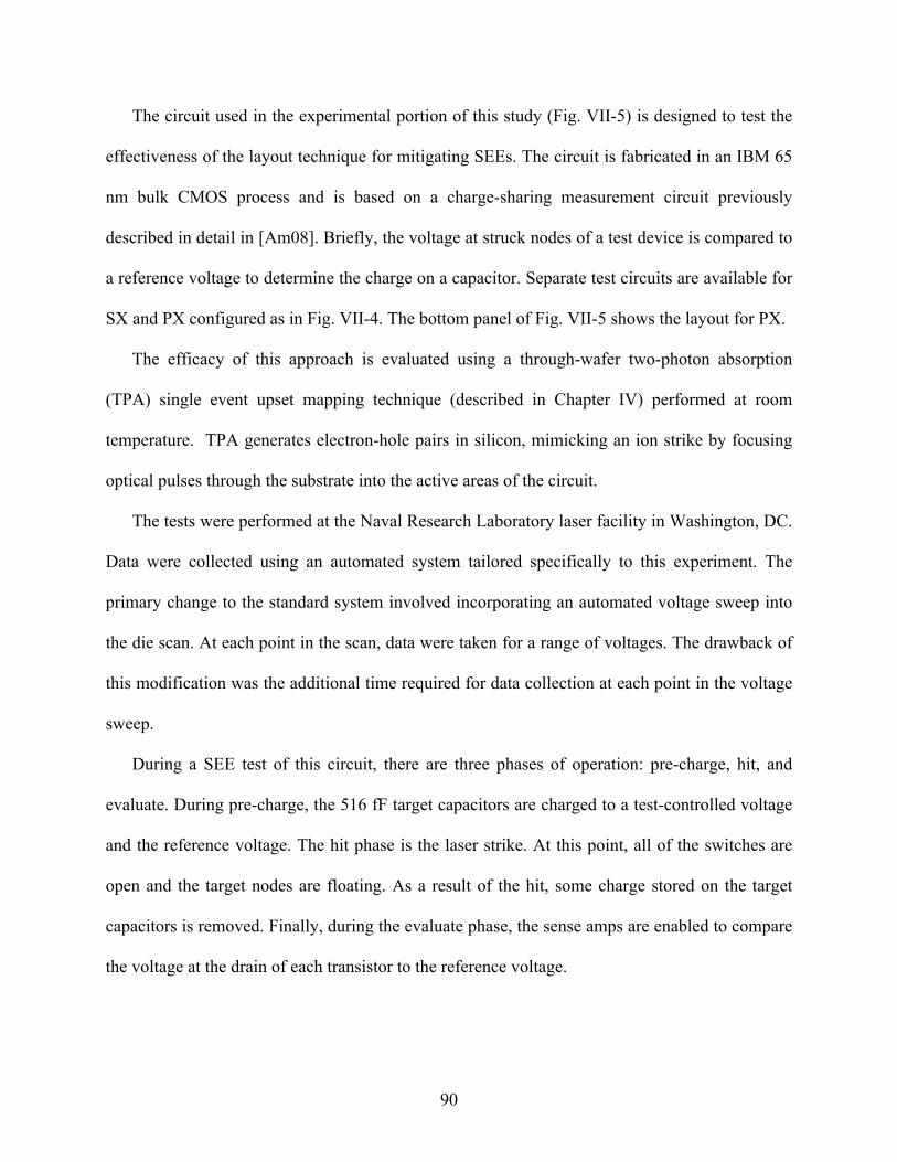
90
The circuit used in the experimental portion of this study (Fig. VII-5) is designed to test the
effectiveness of the layout technique for mitigating SEEs. The circuit is fabricated in an IBM 65
nm bulk CMOS process and is based on a charge-sharing measurement circuit previously
described in detail in [Am08]. Briefly, the voltage at struck nodes of a test device is compared to
a reference voltage to determine the charge on a capacitor. Separate test circuits are available for
SX and PX configured as in Fig. VII-4. The bottom panel of Fig. VII-5 shows the layout for PX.
The efficacy of this approach is evaluated using a through-wafer two-photon absorption
(TPA) single event upset mapping technique (described in Chapter IV) performed at room
temperature. TPA generates electron-hole pairs in silicon, mimicking an ion strike by focusing
optical pulses through the substrate into the active areas of the circuit.
The tests were performed at the Naval Research Laboratory laser facility in Washington, DC.
Data were collected using an automated system tailored specifically to this experiment. The
primary change to the standard system involved incorporating an automated voltage sweep into
the die scan. At each point in the scan, data were taken for a range of voltages. The drawback of
this modification was the additional time required for data collection at each point in the voltage
sweep.
During a SEE test of this circuit, there are three phases of operation: pre-charge, hit, and
evaluate. During pre-charge, the 516 fF target capacitors are charged to a test-controlled voltage
and the reference voltage. The hit phase is the laser strike. At this point, all of the switches are
open and the target nodes are floating. As a result of the hit, some charge stored on the target
capacitors is removed. Finally, during the evaluate phase, the sense amps are enabled to compare
the voltage at the drain of each transistor to the reference voltage.
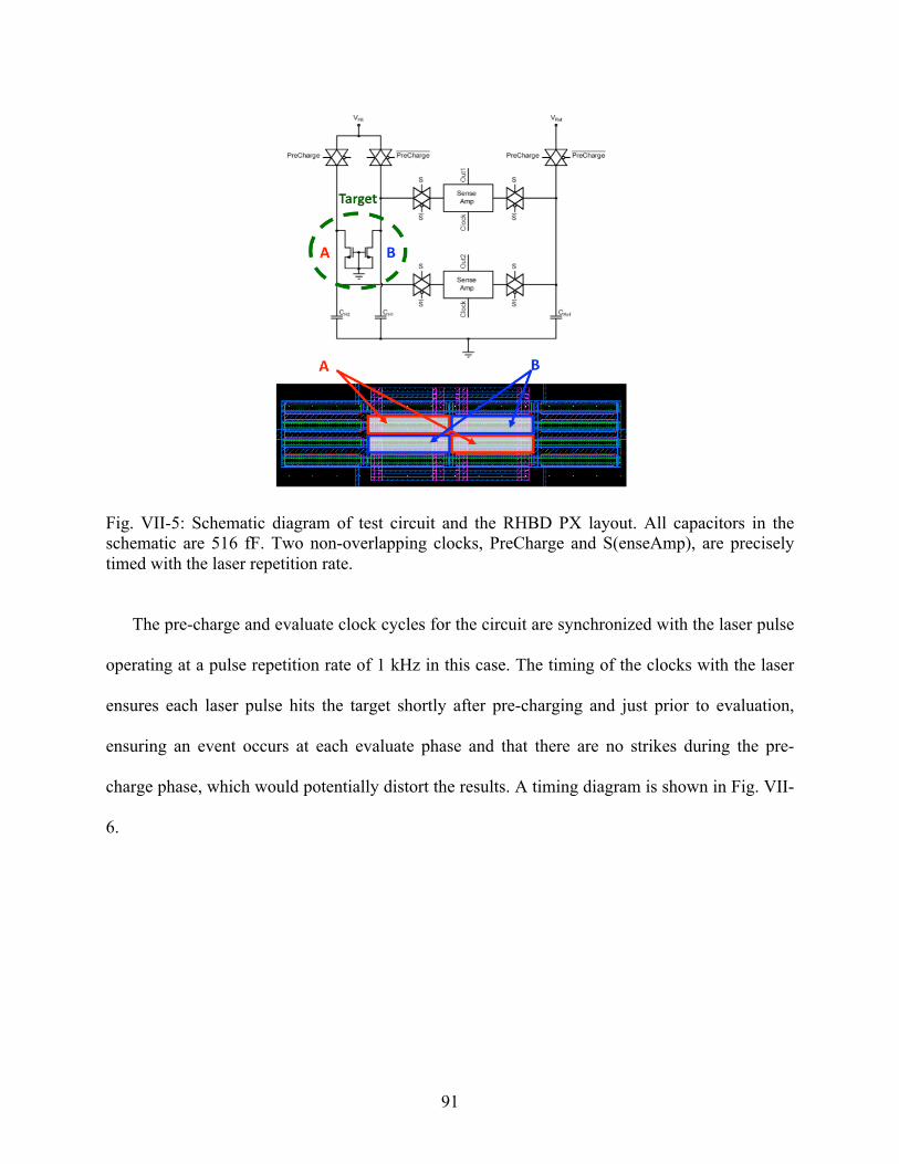
91
Fig. VII-5: Schematic diagram of test circuit and the RHBD PX layout. All capacitors in the schematic are 516 fF. Two non-overlapping clocks, PreCharge and S(enseAmp), are precisely timed with the laser repetition rate.
The pre-charge and evaluate clock cycles for the circuit are synchronized with the laser pulse
operating at a pulse repetition rate of 1 kHz in this case. The timing of the clocks with the laser
ensures each laser pulse hits the target shortly after pre-charging and just prior to evaluation,
ensuring an event occurs at each evaluate phase and that there are no strikes during the pre-
charge phase, which would potentially distort the results. A timing diagram is shown in Fig. VII-
6.
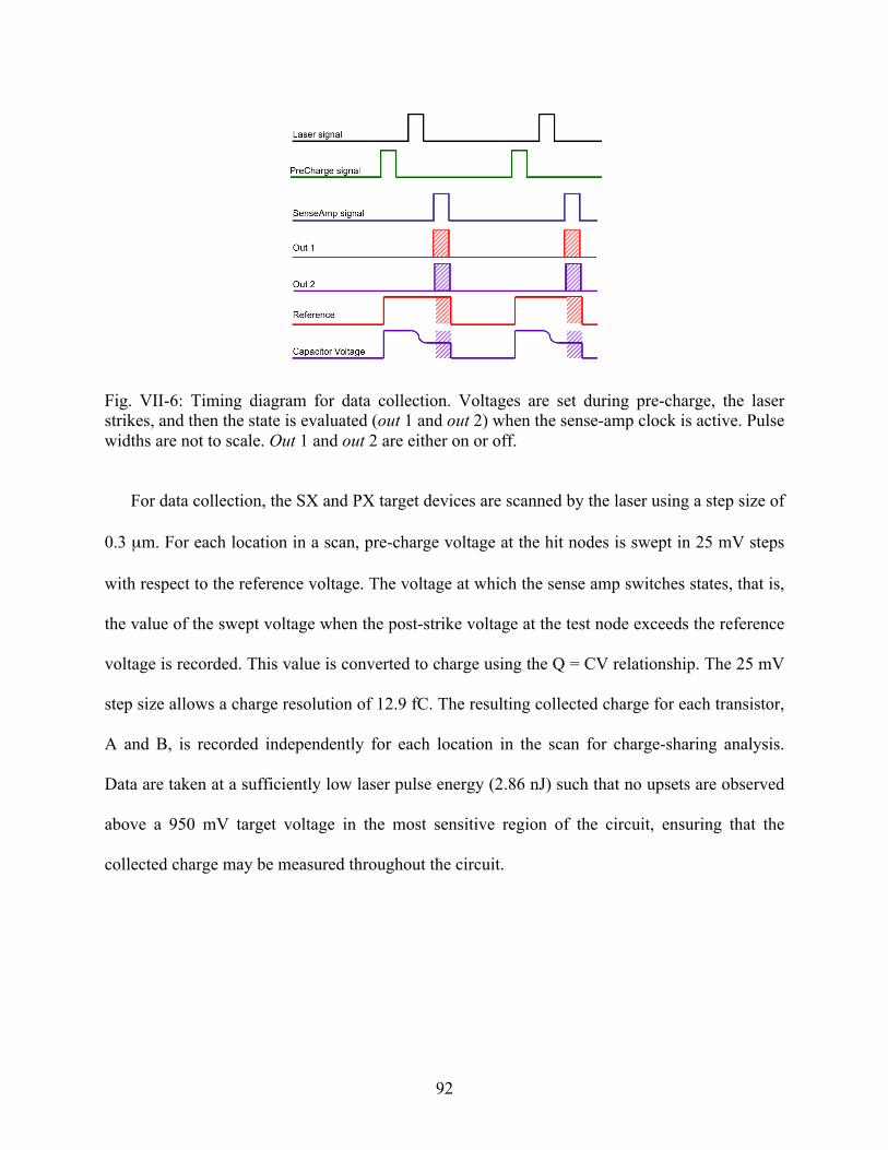
92
Fig. VII-6: Timing diagram for data collection. Voltages are set during pre-charge, the laser strikes, and then the state is evaluated (out 1 and out 2) when the sense-amp clock is active. Pulse widths are not to scale. Out 1 and out 2 are either on or off.
For data collection, the SX and PX target devices are scanned by the laser using a step size of
0.3 µm. For each location in a scan, pre-charge voltage at the hit nodes is swept in 25 mV steps
with respect to the reference voltage. The voltage at which the sense amp switches states, that is,
the value of the swept voltage when the post-strike voltage at the test node exceeds the reference
voltage is recorded. This value is converted to charge using the Q = CV relationship. The 25 mV
step size allows a charge resolution of 12.9 fC. The resulting collected charge for each transistor,
A and B, is recorded independently for each location in the scan for charge-sharing analysis.
Data are taken at a sufficiently low laser pulse energy (2.86 nJ) such that no upsets are observed
above a 950 mV target voltage in the most sensitive region of the circuit, ensuring that the
collected charge may be measured throughout the circuit.

93
Experimental Results The results of the scans for the transistors of SX and PX are normalized with respect to the
maximum collected charge in their respective scans to remove die-to-die and day-to-day
variations in the data caused by experimental error. To quantify the improvement in net collected
charge over an isolated device, data from one transistor of each layout configuration are used as
the charge that would be collected by an individual, isolated transistor. This is possible because
the laser generates enough charge that the individual transistors are not competing for the charge.
These values are referred to as baseline-single-transistor (BLSX) or baseline-parallel-transistor
(BLPX) in the data.
Due to time limitations, only a portion of each device was scanned during test. Care was
taken during design to ensure a symmetric response of the circuit to enable the mirroring of the
data to complete the scans for analysis. Efforts were made to make the analyzed area for both
layout configurations comparable.
To illustrate the improvement in SE response due to the layout technique, the amount of
charge collected by each transistor, A and B, at each location in the scan is measured as
described in the previous section. When one transistor collects more charge than the other, the
“excess” charge is recorded as the differential charge at that point for the transistor having the
larger charge. For example, if A has an experimental charge of 30 fC and B has a charge of 50 fC
for the same scan location, B has a differential charge of 20 fC in that location.
Fig. VII-7 shows a surface plot of the charge of BLSX and BLPX and the differential charge
of transistor A in SX and PX. Qualitatively, the differential charge shows significant
improvement over the baseline case with an approximate improvement of 40% to 60% in the
peak collected charge for SX and PX, respectively. For clarity, the results for transistor B are
omitted from figures, as they are symmetrical to the results of A.

94
Fig. VII-7: Surface plots of charge collected at points in the die scan. Charge collected by a single transistor for each configuration, BLSX (left) and BLPX (right), is shown in the top row. Differential charge is shown in the bottom row for SX (left) and PX (right).
Fig. VII-8 shows a distribution of collected charge versus device area to enable direct
comparison of and to quantify improvement of the sensitive area of the devices. This figure,
based on the concept of a cumulative distribution function (CDF), shows the amount of area (x-
coordinate) that collects an amount of charge (y-coordinate) or less in the device for each of the
four scenarios. The total area for the SX and PX layouts is 46 µm2 and 49 µm2, respectively. As
an example, for a theoretical critical charge (Qc) of 100 fC, the BLSX data show that
approximately 41 µm2 of the 45.9 µm2 die collects at least 100 fC of charge. Said another way,
4.9 µm2 of the device area collects charge greater than Qc. In this case, BLSX would have a
sensitive area of 4.9 µm2.
Table VII-1 is a summary of the sensitive area results with an arbitrary threshold of 100 fC.
SX shows an improvement of 49% over the baseline case while PX shows a 93% improvement.

95
The increased perimeter of the BLPX scenario accounts for the collected charge larger than that
of the BLSX device. This increased perimeter in the PX case is also the source of the
improvement over the SX scenario.
Fig. VII-8: Distribution of collected charge versus device area. Shows the amount of area (x-coordinate) that collects an amount of charge (y-coordinate) or less in the device for each of the four scenarios from left to right: BLPX, BLSX, SX, PX. The total area for the SX and PX layouts is 46 µm2 and 49 µm2, respectively.
Table VII-1: Sensitive areas collecting differential charge greater than 100 fC for Baseline and DCC SX and PX
SX (µm2) PX (µm2) Baseline 10.26 15.84 DCC 5.22 1.08
Sensitive Node Active Charge Cancellation Recent work has developed an effective mitigation technique called sensitive node active
charge cancellation (SNACC) that relies on charge sharing and a current source that becomes
active in the case of a SET event [Bl10]. The key concept of the technique is to create a circuit
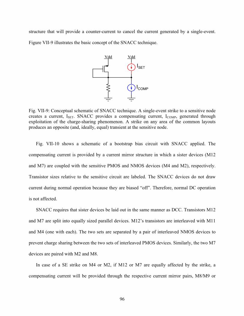
96
structure that will provide a counter-current to cancel the current generated by a single-event.
Figure VII-9 illustrates the basic concept of the SNACC technique.
Fig. VII-9: Conceptual schematic of SNACC technique. A single-event strike to a sensitive node creates a current, ISET. SNACC provides a compensating current, ICOMP, generated through exploitation of the charge-sharing phenomenon. A strike on any area of the common layouts produces an opposite (and, ideally, equal) transient at the sensitive node.
Fig. VII-10 shows a schematic of a bootstrap bias circuit with SNACC applied. The
compensating current is provided by a current mirror structure in which a sister devices (M12
and M7) are coupled with the sensitive PMOS and NMOS devices (M4 and M2), respectively.
Transistor sizes relative to the sensitive circuit are labeled. The SNACC devices do not draw
current during normal operation because they are biased “off”. Therefore, normal DC operation
is not affected.
SNACC requires that sister devices be laid out in the same manner as DCC. Transistors M12
and M7 are split into equally sized parallel devices. M12’s transistors are interleaved with M11
and M4 (one with each). The two sets are separated by a pair of interleaved NMOS devices to
prevent charge sharing between the two sets of interleaved PMOS devices. Similarly, the two M7
devices are paired with M2 and M8.
In case of a SE strike on M4 or M2, if M12 or M7 are equally affected by the strike, a
compensating current will be provided through the respective current mirror pairs, M8/M9 or

97
M10/M11, and will effectively cancel out the charge at the output and therefore, mitigate the
transient.
The SNACC technique adds capacitance to the node, which, in the case of a high-speed
circuit, may eliminate SNACC as a hardening option. However, this same quality makes SNACC
a very good candidate for DC circuits. There is also an area penalty for SNACC, but is typically
much smaller than the area of a filtering capacitor that provides the same level of mitigation
[Bl10].
Fig. VII-10: Bootstrap current source with SNACC applied. Transistors M7-M12 are the devices added for the SNACC technique. M1-M4 are the core bootstrap device and M5 and M6 make up start-up circuitry. Figure from [Bl10].
Conclusions
Background information for RHBD techniques used throughout the rest of this paper is
presented in this chapter. Each technique has benefits and penalties. The choice of applied
technique depends on the application and the circuit type. This is the primary topic for the
remainder of the dissertation.

98
CHAPTER VIII
SINGLE-EVENT CHARACTERIZATION AND HARDENING OF CML CIRCUITS
Introduction
This chapter introduces the results of hardening CML circuits. These occur in the data (pre-
amplifier) and timing (phase rotator) circuitry. In depth discussion of the pre-amplifier hardening
is presented first. Results for the phase rotator circuitry are then presented. The outcome of this
chapter is to identify the RHBD design considerations and establish recommendations for CML
hardening.
Pre-Amplifier CML Hardening
Experimental results of the 6 dB pre-amplifier presented in Chapter V indicate SE sensitivity
in the T9/T10 differential amplifier (Fig. VIII-1). The reason for this sensitivity was theorized to
be a result of an off-chip bias at a current that caused the mirror devices to operate near the
ohmic region. Simulations of the circuit as implemented in the full system indicate that altered
biasing mitigates SETs to above an LET of 40 MeV-cm2/mg. However, these simulations have
the differential amplifiers biased at a high current partly in the spirit of maintaining a fast
switching time and partially in the spirit of driving the communications channel. Regardless, the
increased current provides charge dissipation hardening. This section shows that even with
reduced or non-ideal biasing, as seen in the experimental data, DCC can be useful for mitigating

99
SETs in CML circuitry, and establishes the technique as a recommended standard practice in
CML circuit design.
Fig. VIII-1: Simplified 6 dB pre-amp used in experiments. T0/T1 and T9/T10 are the differential amplifiers, T2/T3 is the output stage, and the current mirror includes each of the transistors at the bottom of the figure. The current drive increases from left to right on the schematic. Unlike the simulated device, the bias point is set off-chip.
PDS in Pre-Amplifier
To definitively establish the cause of the sensitivity in the T9/T10 differential amplifier,
phase-dependent sensitivity (PDS) analysis is performed on the 4.6 pJ TPA data presented in
Chapter V. Errors are defined as local maxima or minima with values less than 50% of the
average maximum or minimum voltage of the transient (an example transient Fig. VIII-2).

100
Fig. VIII-2. Sample transient for a bit upset in T0/T1 resulting from a laser pulse energy of 6.9 nJ. This is a typical example of the observed bit upsets throughout the circuit. The shaded region indicates the areas in which an error is identified. In this case, the error threshold is 50% of the average peak voltage.
Fig. VIII-3 shows the number of errors in the scan binned with respect to the time of the laser
strike in the data cycle. A sinusoidal signal with ideal output characteristics is overlaid for
correlation with the binned data. The vulnerable portion of the data cycle is shown for the
positive (Fig. VIII-3a) and negative (Fig. VIII-3b) outputs of the circuit (OUTP and OUTM,
respectively) during a scan of the differential-pair transistors T9 and T10. The error profiles for
the two outputs indicate the sensitive time in the cycle as the negative portion of the cycle, i.e.,
data LOW.

101
(a) (b)
Fig. VIII-3: Histograms of error counts superimposed on the data cycle for the outputs of a scan of the device operating at 2 Gbps with an incident laser energy of 4.6 nJ. OUTP (a) shows fewer errors overall than (b) OUTM due to excess noise on the OUTM signal. Errors are binned according to the time in the data cycle the laser struck the device.
The PDS data provides the designer with a tool to determine the vulnerable percentage of the
data cycle and assess the operating state of the scanned device during the vulnerable time, similar
to the knowledge gained when performing a WOV analysis of a digital circuit. As an example,
the data presented in Fig. VIII-3 show errors concentrated in the latter portion of the data cycle.
Through circuit analysis (see Fig. VIII-1) and from knowledge of the test setup, this confirms
that the cause for the errors is related to the biasing of the circuit. During the experiment, T9 and
T10 were biased in such a way that when one side of the differential amplifier is pulling the
majority of the tail current (during the extremes of the data cycle), the other transistor falls into
the ohmic operating region. Any perturbation due to single events on the gate of a transistor
operating in the ohmic region causes large fluctuations in current in the ohmic device. The
disparity in number of errors between the OUTP and OUTM data is due to the area of T9 being
truncated during the scan.

102
Using this information, an informed decision as to the proper hardening technique can be
made. In this case, DCC is applied to T9/T10 to illustrate the effectiveness of the technique even
with non-ideal bias conditions.
SEE Hardening of the Pre-Amplifier
CML In the previous sections of this chapter, the vulnerability of the differential amplifier
involving T9 and T10 is shown and attributed to poor bias conditions. The options for hardening
the CML portion of the circuit include charge dissipation, filtering, DCC, and SNACC, as
described in Chapter V.
As noted in the simulation results, the differential amplifiers are not sensitive to SEE up to an
LET of 40 MeV-cm2/mg. This is due to the prescribed changes to the bias conditions and the use
of charge dissipation. In simulations of the circuit in Fig. V-2, the most sensitive nodes are the
current amplifier inputs to the first CML buffer. However, to test the efficacy of the DCC
technique in a CML circuit not optimally biased, simulations are run on the experimental circuit
(Fig. VI-3).
The voltage-dependent models described in Chapter IV are employed to simulate charge
sharing in the differential amplifiers in the circuit of Fig. VIII-1. Electrical models for the IBM
90 nm CMOS9SF process are employed along with the experimental results for charge collected
on the 65 nm DCC structures described in Chapter VII. The experimental results, though from a
65 nm process as opposed to the 90 nm process of the test circuit, effectively show the benefits
of the DCC layout technique. The results are intended to demonstrate the effectiveness of DCC
using charge values gathered from physical devices in a DCC configuration.

103
Four scenarios are simulated. The first two, the baseline case, single (BLSX) and parallel
(BLPX) unit-cell devices configured as in Fig. VII-4 (previous chapter), in a standard common-
centroid layout with sources adjacent, are simulated with a normal-incidence SE strike with
charge collected by T9. The SE model is then configured for normal-incidence charge sharing.
Each layout configuration is simulated with DCC applied: the DCC single transistor (DCC SX),
and the DCC parallel transistors (DCC PX). The layout of the DCC transistors is configured as in
the baseline case, but with the drains of the devices in close proximity. The values of generated
charge for the devices in each simulation are extracted from experimental data from Chapter V
and are summarized in Table VIII-1. Resulting transients are shown in Fig. VIII-4. The vertical
line indicates the time of the maximum voltage excursion from the control case.
The models are configured to simulate a normal-incidence strike, to best emulate the laser
environment. Multiple simulations are run simulating the SE over the entire clock cycle, to
ensure coverage of the highest phase sensitivity of the circuit. Resulting average and maximum
output voltage excursions are shown in the legend of Fig. VIII-4.
Table VIII-1: Simulated charge on T9 and T10 in each of the four simulated scenarios T9 (fC) T10 (fC) BLSX 206.4 0 BLPX 270.9 0 DCC SX 165.12 41.28 DCC PX 189.63 81.27

104
Fig VIII-4: Simulated transients at the outputs of the circuit in Fig. VIII-1 for strike conditions listed in Table VIII-1. The vertical line indicates the point of greatest excursion from the no-strike condition.
Improvement in circuit behavior is seen in both the SX and PX cases. From the baseline to
the charge-sharing case, the maximum output excursion improved by 39% and 56% for the
matched and centroid layouts, respectively. Greater improvement would be expected for an
angled strike because the charge sharing would be more equal. These improvements put into
context the significant improvement in a circuit application, even under non-ideal bias
conditions.
Phase Rotator
The phase-rotator mixer circuit shown in Fig. VIII-5 is simulated with DCC applied to the
circled nodes via the voltage-dependent model and the calibrated 90 nm values for charge-
sharing at 0˚ and 60˚ strikes. The transmission-gate input nodes, labeled “A”, with opposite
signals (0/180 and 90/270) of the same channel type (NMOS or PMOS) are paired as described

105
in Fig. VIII-6. The remainder of the devices are paired as circled. Significant improvement is
shown for error counts at each DCC pair (see Table VIII-2).
Table VIII-2: Error count for phase rotator for DCC hardened and unhardened circuits. Node B is not simulated for P-strikes.
Node LET (MeV-cm2/mg)
# Errors (Unhard. N-strike)
# Errors (DCC 0˚ N-strike)
# Errors (DCC 60˚ N-strike)
# Errors (Unhard. P-strike)
# Errors (DCC 0˚ P-strike)
# Errors (DCC 60˚ P-strike)
Node A 20 4 0 0 2 0 0 30 12 5 0 7 0 0 40 14 6 5 8 0 4 Node B 30 4 0 0 n/a n/a n/a 40 10 4 0 n/a n/a n/a Node D 20 6 2 0 2 0 0 30 7 4 1 2 0 0 40 10 4 6 6 0 2
Fig. VIII-5: Phase rotator schematic with DCC sister devices identified. The transmission gate nodes are laid out as shown in Fig. VIII-6. The differential sister pairs are laid out in a similar fashion or as shown in Fig. VII-4.
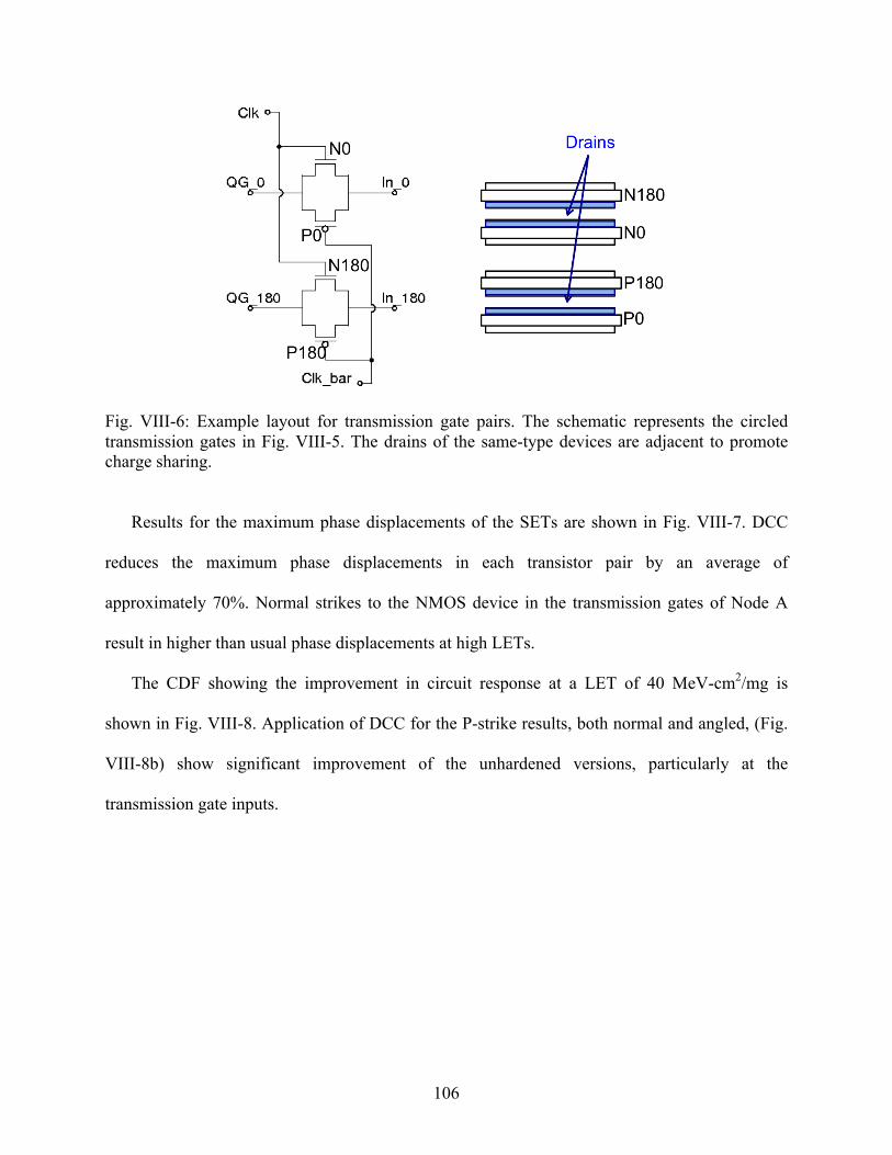
106
Fig. VIII-6: Example layout for transmission gate pairs. The schematic represents the circled transmission gates in Fig. VIII-5. The drains of the same-type devices are adjacent to promote charge sharing.
Results for the maximum phase displacements of the SETs are shown in Fig. VIII-7. DCC
reduces the maximum phase displacements in each transistor pair by an average of
approximately 70%. Normal strikes to the NMOS device in the transmission gates of Node A
result in higher than usual phase displacements at high LETs.
The CDF showing the improvement in circuit response at a LET of 40 MeV-cm2/mg is
shown in Fig. VIII-8. Application of DCC for the P-strike results, both normal and angled, (Fig.
VIII-8b) show significant improvement of the unhardened versions, particularly at the
transmission gate inputs.

107
(a)
(b)
Fig. VIII-7: Maximum phase displacement for the N-strike (a) and P-strike (b) results for the CML subcircuit of the phase-rotator shown in Fig. V-15. Points in the shaded region are considered errors. The filled symbols indicate normal incidence simulations, the hollow symbols indicate simulated angled strikes.

108
(a)
(b)
Fig. VIII-8: CDF for DCC hardened phase rotator for N-strikes (a) and P-strikes (b). The left graph in each figure shows results for normal-incidence simulations, the right panel shows results for 60-degree incidence. Phase displacements to the right of the dotted line are considered errors.

109
Conclusions
The presented results indicate the suitability of DCC hardening in the case of CML circuitry
in either the data or clock path. It is important to design the circuits to keep the differential
transistors operating in saturation, otherwise, the circuit is vulnerable to SEEs. However, to
further insure against unwanted transients, it is recommended that the pairs of transistors employ
DCC, as a RHBD default.

110
CHAPTER IX
SINGLE-EVENT CHARACTERIZATION AND HARDENING OF DOMAIN INTERFACE
CIRCUITS
Introduction
This chapter presents results and hardening techniques for the domain interface circuits.
Again, DCC techniques are highlighted as effective mitigators of SETs in these important
circuits. Errors in the CML to CMOS block of the phase rotator are characterized and the circuit
hardening technique is described. In addition, SETs in the CMOS to CML portion of the pre-
amplifier circuit and the interface between CML and CMOS and the clock signal in the
comparator are presented. The outcome of this chapter is to identify the RHBD design
considerations and establish recommendations for domain interface hardening.
Phase Rotator CML to CMOS
Clock and Data Recovery
A high-speed communications system with multiple lanes such as a XAUI interface,
typically utilizes a system-wide phase-locked-loop- (PLL) based clock that is distributed to each
of four lanes. The timing of each lane is independent until the signals are recombined after the
data are deserialized. The distributed clock is retimed within the independent lanes to match the
received differential serial data. The in-lane timing is accomplished within the CDR via a
current-mode phase-rotator (see Fig. IX-1a). The resulting signal is converted to full-swing

111
CMOS logic in the CML to CMOS circuit block to be fed back to the input of the CDR
comparator.
The CML signal is converted to a full-swing CMOS logic signal through a design shown in
the schematic in Fig. IX-1b. In this circuit, the CML signal is input as a differential controlling
voltage on a current amplifier. The current-based clock signal is propagated to a cross-coupled
common-source amplifier. The output of this amplifier goes to the input of a regenerative
inverter that provides a full-swing output voltage.
This conversion from CML to CMOS is necessary to ensure the decision threshold of the
inverter is met with each clock swing. The consequence of an error in the CML to CMOS circuit
is a missed clock cycle in the comparator of the CDR and can result in mistimed data.
(a) (b)
Fig. IX-1: Block diagram of a typical receiver and CDR circuit (a). The CML to CMOS block converts the incoming PLL clock to CMOS logic for use in timing the CDR comparator. All signals are differential. CML to CMOS circuit (b) derived from [Ema07]. The limited swing of the CML inputs are translated to full-swing CMOS outputs through current-based data to a regenerative inverter pair. The CML inputs are received from the PLL clock that has been rotated to match incoming receiver data. The CMOS outputs are fed back into the CDR comparator to provide timing information.

112
Circuit Hardening for SEE Mitigation & Results In this section the charge dissipation and DCC techniques are applied to the baseline CML to
CMOS circuit to provide a direct comparison of the techniques. Simulations are run as described
in the previous section.
Charge Dissipation Results
Transistor widths are incrementally increased until no phase displacements exceeded a π-
radian threshold. In this case, the transistor widths of all devices except those in the regenerative
inverter are quadrupled. The additional current increases the power consumption of the circuit
from 3 mW to 21.7 mW. This design change also increased the active area of the circuit four-
times over.
Maximum and average phase displacements are shown along with the worst-case (net1)
baseline results in Fig. IX-2. The maximum phase displacements of net1 begin to exceed the
error threshold at an LET of 20 MeV-cm2/mg. At all nodes, the average phase displacements are
well within specifications and show at least an 80% improvement over the baseline average.
Figure IX-3 shows the CDF with the baseline and charge dissipation results. Nets 3 and 5 are
within the error range but approximately 9% of events from net1 fall outside the error criteria.
Overall, 2.3% of the displacements are out of specifications, as compared to 3.5% in the
unhardened circuit. These results indicate a significant improvement in single-event response for
this technique.

113
Fig. IX-2: Maximum and average phase displacement for SE strikes in the circuit hardened by increased currents along with the baseline results (small icons and dotted lines). Events above the dotted lines are considered errors. The results for net5 fall in line with net3.
Fig. IX-3: CDF for charge dissipation hardening scheme. The shift of the results to the left indicates an improvement in the hardening of the circuit. Events to the right of the vertical line are considered errors.

114
DCC Results The voltage-dependent SET models described in Chapter IV have a charge-sharing feature
calibrated to experimental results for this 90 nm technology [Ka09]. This feature is necessary to
accurately simulate the key mechanism of DCC. This model incorporates the effects of charge
sharing between adjacent devices for normal and 60-degree strikes.
The baseline circuit is analyzed for transistor pairs that provide a complementary response.
These pairs are indicated in Fig. IX-4 and are simulated such that a strike to one transistor results
in charge collection on the sister device. To fully realize the potential of the DCC technique, the
baseline topology is modified by removing MP7 and MP8 (see Fig. IX-1b) and linking the tail
current devices with a 2.5-kΩ resistor. Transistors F1 and F2 are laid out as DCC sister devices.
Under normal operation, the added resistor maintains separation between nets 1 and 2, but the
resistor allows current from the sister device to act as a single tail current and maintain operation
in case of a SE strike.
Fig. IX-4: CML to CMOS circuit with DCC devices indicated. The transistor pairs are laid out similar to a common-centroid layout, but ensuring the drains are as close in proximity as allowed by layout design rules. The circled area of the schematic indicates the design modification. The resistor is 2.5 kΩ.
115
The removal of MP7 and MP8 is key to the success of DCC at net1. The primary cause of
disruptive transients on this node is due to a lack of headroom with the 1 V rail voltage and
three-transistor stack (two PMOS and one NMOS device). It takes little generated charge to
force the transistors, NMOS or PMOS, out of saturation. The functionality of MP7 and MP8 is to
improve the matching of MP1 and MP2. However, with the recommended DCC layout, the
physical match is sufficient for a rail-to-rail CMOS output.
Figure IX-5 shows the maximum and average phase displacement results of the circuit
response with DCC implemented for normal (Fig. IX-5a) and angled (Fig. IX-5b) strikes to the
pairs of sister devices. There is little improvement over the baseline phase displacement for the
maximum strikes at normal incidence. The irregular maximum phase displacement values for
net3 for LETs 20 - 40 MeV-cm2/mg in Fig. IX-5a and the large increase in the maximum phase
displacement for net1 at an LET of 40 MeV-cm2/mg in Fig. IX-5b result from the net charge on
the node and the ratio of the charge collected by devices A1 and A2, and F1 and F2, respectively.
Normal strikes on net1 show the least amount of improvement in the average phase displacement
over the unhardened circuit, yet still improved the average by 50% over the unhardened circuit.
The angled strikes show an improvement on the average phase displacement on par with the
charge dissipation results, approximately 80%.
The CDF results for DCC at normal and angled incidences are shown in Fig. IX-6. Normal-
incidence strikes on net1 result in errors in approximately 2.2% of the events, angled strikes
result in errors in approximately 0.4% of the events. Normal and angled strikes result in errors
over all of the nets in 1.5% and 0.25% of the events, respectively. This is a significant
improvement over the baseline circuit.
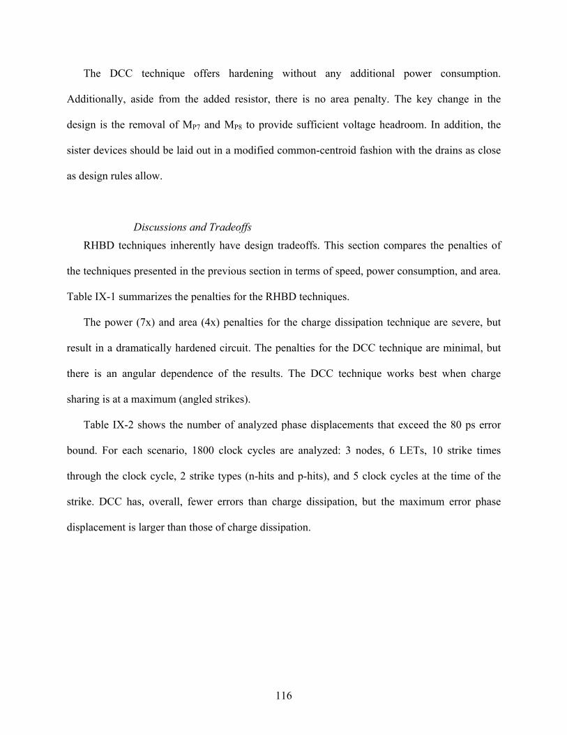
116
The DCC technique offers hardening without any additional power consumption.
Additionally, aside from the added resistor, there is no area penalty. The key change in the
design is the removal of MP7 and MP8 to provide sufficient voltage headroom. In addition, the
sister devices should be laid out in a modified common-centroid fashion with the drains as close
as design rules allow.
Discussions and Tradeoffs RHBD techniques inherently have design tradeoffs. This section compares the penalties of
the techniques presented in the previous section in terms of speed, power consumption, and area.
Table IX-1 summarizes the penalties for the RHBD techniques.
The power (7x) and area (4x) penalties for the charge dissipation technique are severe, but
result in a dramatically hardened circuit. The penalties for the DCC technique are minimal, but
there is an angular dependence of the results. The DCC technique works best when charge
sharing is at a maximum (angled strikes).
Table IX-2 shows the number of analyzed phase displacements that exceed the 80 ps error
bound. For each scenario, 1800 clock cycles are analyzed: 3 nodes, 6 LETs, 10 strike times
through the clock cycle, 2 strike types (n-hits and p-hits), and 5 clock cycles at the time of the
strike. DCC has, overall, fewer errors than charge dissipation, but the maximum error phase
displacement is larger than those of charge dissipation.

117
(a)
(b)
Fig. IX-5: Maximum and average phase displacement results of DCC hardening at normal (a) and 60-degree angle (b). In all cases, improvement is seen over the unhardened circuit. Events above the dashed lines are considered errors.
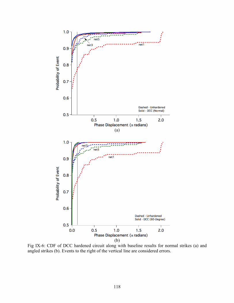
118
(a)
(b)
Fig IX-6: CDF of DCC hardened circuit along with baseline results for normal strikes (a) and angled strikes (b). Events to the right of the vertical line are considered errors.

119
The ultimate decision as to which hardening technique is used depends on the specific
application. If power and area are not a concern, the relatively small effort in modifying the
layout of a circuit with increased current drive may drive a designer to choose charge dissipation.
On the other hand, area and power penalties may deter the designer from using charge
dissipation or may encourage a combination of charge dissipation and DCC. In this case, it is not
advantageous to combine the two techniques because any increase in size of devices in the
current amplifiers leads to higher current gain, which amplifies any remaining errors.
Table IX-1: Design penalties of charge dissipation (CD) and differential charge cancellation (DCC) RHBD techniques.
CD DCC Power 7x None Area 4x Minimal
Speed None None
Table IX-2: Number of errors (phase displacements exceeding 80 ps) for unhardened, charge dissipation (CD), and DCC at normal (DCC0) and angled (DCC60) strikes.
Unhardened CD DCC0 DCC60 Net1 90 77 22 5 Net3 13 2 13 4 Net5 23 2 20 0 Total 126 81 55 9
Comparator CML to CMOS with Clock
DCC is applied to three nodes of the simulated comparator circuit. These are the
complementary nodes of Data, Latch, and Out, as identified in Fig. IX-7. Again, errors are
counted as when the output of the latches switches states. Because the timing of the circuit is
driven by the clock received from the phase rotator, a full set of simulations are run with the

120
clock rotated with respect to the data to determine any phase-related sensitivity. These errors are
counted in the tally in Table IX-3. The DCC technique is shown to be effective in reducing the
number of errors at each node.
Fig. IX-7: Simulated schematic of comparator. Out_p and Out_n lead to latches that sample the value at the node using the rotated clock. The latched signals, Out_p and Out_n are compared with an XNOR gate to sense an error.

121
Table IX-3: Number of errors for unhardened and hardened comparator at Data, Latch, and Output nodes for unhardened, normal strikes with DCC, and angled strikes with DCC.
Node LET (MeV-cm2/mg)
# Errors (Unhardened)
# Errors (0˚ Strike)
# Errors (60˚ Strike)
Data 5 0 0 0 10 4 3 5 20 9 5 5 30 17 9 9 40 20 16 11
Latch 5 6 3 4 10 11 11 5 20 13 12 9 30 16 13 14 40 17 12 14
Node 5 5 4 1 10 9 8 7 20 11 10 10 30 16 11 12 40 16 13 13
Pre-Amplifier CMOS to CML
The simulations of the pre-amplifier show the CMOS to CML circuitry to be the most
sensitive nodes to SET in the correctly-biased pre-amplifier circuit. When the complementary
nodes (Data_P/Data_N and NodeA/NodeB from Fig. IX-8) from the inputs are subjected to the
DCC technique, results show an improvement in the maximum phase displacements (Fig. IX-9).
The CDF plot also shows improvement as seen in Fig. IX-10.
Fig. IX-8: Simulated pre-emphasis and buffer schematic. Data_P and Data_N are paired using the DCC technique as are Data_P/N and NodeT_P/N.
122
Fig. IX-9: Maximum phase displacement results for strikes on Data_P and Node A of the pre-amplifier shown in Fig. IX-X.
Fig. IX-10: CDF plot for nodes Data_P and Node A for hardened and unhardened conditions. The inset figure shows a magnification of the upper-left corner of the larger figure.

123
Conclusions
The presented results indicate the suitability of DCC hardening in the case of domain
interfaces circuitry in both the data or clock path. Identification of opportunities to exploit the
differential nature of the circuitry is important. In the phase rotator’s CML to CMOS circuit,
because of the cross-coupled devices in the circuit, DCC sister pairs are not mirror images. In
addition, the phase-rotator CML to CMOS circuit was modified to create an effective single tail
current on the inputs of the device. This modification allows DCC to be applied to the NMOS
and PMOS devices at this node.
124
CHAPTER X
RHBD GUIDELINES
The single-event (SE) characterization of high-speed communications systems finds common
vulnerabilities at signal domain interfaces, in CML circuits, and in bias circuits. The previous
chapters show hardening techniques for the domain interface and CML sensitivities. The
cumulation of these studies lead to three general RHBD guidelines for the design of high-speed
communications systems.
Guideline 1: RHBD in Signal Domain Interfaces
Domain-interface errors occur in the system where the data signal is transferred from full-
swing digital to CML or vice-versa, typically a mixed-signal circuit. This transition occurs
within the pre-emphasis stage in the transmitter when CMOS logic is converted to CML. The
timing feedback of the CDR in the receiver includes circuitry to convert CML to CMOS logic.
These interfaces are within the signal and clock classifications and often employ current
amplifiers to make the transition to/from full/limited swing. The DCC technique is used to
mitigate these errors.
To accurately characterize the SE response of the signal-domain interfaces, care must be
taken while determining the division of subcircuits for simulation and/or experiment. The
transition from one signal domain to another should not be divided between two subcircuits for
either simulation or experiment. This may involve using the output stage of one subcircuit as the

125
first stage of the next or the input stage. For example, in the original SerDes transmitter circuit
used in this dissertation, the level shifter was split at the “Data_N” and “Data_P” nodes (see Fig.
X-1). Recall the differing inputs for simulation and experiment in Fig. V-1. Simulation only
finds errors when the level shifter is simulated with the pre-amplifier. The described
experimental test structure does not test the domain interface at all.
The determination of “sister devices” in the circuits is the key to successful application of
DCC in the translating circuits. In most circuits, such as the pre-amplifier, DCC is applied to the
complementary devices as seen in Fig. X-1. At times, the sister devices are not as obvious, such
as in the CML to CMOS circuit of the phase rotator (Fig. X-2). The cross-coupled current
amplifier makes the device connected to the mirroring structure to have better common rejection
than the complementary differential device. The CML to CMOS circuit also demonstrates how,
with slight modification, DCC can be applied to nodes that would normally not work with the
technique. In this case, MP7 and MP8 are removed and the tail currents on the input pair are
effectively combined, but separated by a resistor. Designers should look for opportunities to
apply DCC whenever possible.
Fig. X-1: Pre-amplifier schematic with DCC sister devices identified. Device pairs ‘A’ and ‘B’ are related to the domain interface errors. Pairs ‘C’ and ‘D’ have DCC applied as part of CML hardening.

126
Fig. X-2: Unhardened CML to CMOS circuit (left) and hardened circuit with DCC sister devices identified (right). Due to the cross-coupled current amplifier, the pairs are not always complementary devices of the differential signal. Also, modification from the original schematic makes DCC possible with device pair ‘F’.
Guideline 2: RHBD in CML
CML errors involve the mixed-signal circuitry in which high-speed data needs to propagate
as efficiently as possible. CML consists of differential amplifiers that operate with a limited
voltage input and output swing. If these circuits are not biased correctly, the transistors may be
forced to operate in the linear region and can become more susceptible to an ion strike. DCC is
also used to mitigate these errors.
It is recommended that all CML differential pairs be laid out with the DCC technique. There
is no penalty for speed, power, or area and DCC provides some protection for cases in which the
bias conditions may not be ideal. These situations could be a poor input value, aging of the
circuit, or even tail current adjustments such as those in the phase rotator. The pre-amplifier

127
circuit with a non-ideal bias (as was used for experiment) shows a 56% improvement in
simulations with DCC applied to T9/T10 (Fig. X-3).
Fig. X-3: Pre-amplifier circuit used in experiment with non-ideal biasing. When DCC is applied to the differential pairs T0/T1 and T9/T10, the SE response is improved by 56%.
Guideline 3: RHBD for Power Circuitry
Bias errors result from SE strikes on DC circuitry. In the circuits simulated for this study, no
significant errors are found in the bias circuits. However, the majority of the currents operate in
the hundreds of micro-amps to tens of milliamps, which, by default, set up a charge dissipation
situation. Also, for noise reduction, low-pass filters are employed throughout the current tree.
Again, the filters aid in the suppression of SETs.
In cases where bias or other single-ended steady-state circuits are not hardened through
convenient charge dissipation and filtering, the SNACC technique is recommended. Like
filtering, the primary penalty of SNACC is area. However, SNACC is more area-efficient than
filtering in terms of single-event amplitude and duration. Recent simulations of SNACC applied
to a bootstrap current source designed in a 90 nm process show more than 60% improvement in
both amplitude and duration of transient. For more information, refer to [Bl11].
Finally, Pin-selectability is convenient in situations where power-down circuitry, alternate
protocols, or test conditions are needed as options. However, the ramifications of the circuitry

128
such as an accidental power-down, a change to a less-than-optional bias condition, or an
inadvertent test condition must be addressed at the time of circuit design by employing SNACC,
TMR, or other traditional hardening technique.
129
CHAPTER XI
CONCLUSIONS
From a system design point-of-view, four primary functions of a communications system
must be considered prior to design: data flow, power, timing, and environment. The architecture
of the device is chosen to optimize the performance in each of these areas based on the intended
operating conditions. Typically, a system is designed as individual functional blocks. For
example, a SerDes system is designed as a transmitter and receiver communicating over a
communications channel. However, if the system is considered as a whole, “global” signals can
be identified: the signal path, bias circuitry (including the power supply), and the clock. These
can be referenced to the primary considerations of system design: data flow, power, and timing,
respectively.
In this work, for the first time, vulnerabilities to SE are identified in circuitries that interface
between signal domains, such as from full-swing digital logic to CML and vice-versa. These
interface circuits are found in the data path and the clock circuitry. Traditional and recently
developed analog RHBD techniques are compared for suitability in high-speed, low-power
applications. In addition, the division of subcircuits with mindfulness to keep together the whole
of the domain interface circuits for simulation and experiment is noted for the first time.
Experimental validation of the DCC technique and simulations using the experimental data
on the pre-amplifier circuit advance the development of this hardening method. The pre-
amplifier simulations indicate that DCC is effective in CML even when the circuitry is not

130
optimally biased. The DCC technique is used throughout this work and found to be the preferred
method of hardening high-speed differential circuits.
DCC is applied to domain-interface circuitries resulting in mitigation of SETs by up to 80%
with no appreciable power, area, or speed penalties. In some cases, it is advantageous to modify
slightly the circuit topology to allow the use of DCC, as seen in the CML to CMOS circuit of the
phase rotator. The DCC layout technique can provide significant improvement in single-event
hardness for a range of high-speed differential circuit designs with minimal impact to the
circuit’s footprint.
While developed for SerDes, the RHBD recommendations can be applied to any CMOS
high-speed communications device. The techniques that exploit charge sharing will only become
more effective as technologies scale. These recommendations are summarized as follows:
1.) Identify domain interface circuitry, do not split the interface over multiple subcircuits,
and apply DCC to sister devices. Be aware that the sister devices are not always the
complementary devices. Modifications to the circuit can make DCC an option,
particularly in the case of tail currents.
2.) Apply DCC to all differential pairs in CML. This provides protection in the case of
varying tail currents, aging, or biasing errors.
3.) Apply SNACC to bias circuitry in low-power scenarios.

131
PUBLICATIONS
Published Journal Articles [1] A. Balasubramanian, O. A. Amusan, B. L. Bhuva, R. A. Reed, A. L. Sternberg, L. W.
Massengill, D. McMorrow, S. A. Nation, and J. S. Melinger, “Measurement and Analysis of Interconnect Crosstalk Due to Single Events in a 90 nm CMOS Technology, “IEEE Trans. Nucl. Sci., vol. 55, no. 4, pp. 2079-2084, Aug. 2008.
[2] O. A. Amusan, P. R. Fleming, B. L. Bhuva, L.W. Massengill, A. F. Witulski, A.
Balasubramanian, M. C. Casey, D. Mcmorrow, S. Nation, F. Barsun, J. S. Melinger, M. Gadlage, and T. D. Loveless, “Laser Verification of On-Chip Charge Collection Measurement Circuit,” IEEE Trans. Nucl. Sci., vol. 55, no. 6, pp. 3309-3313, Dec. 2008.
[3] A. Balasubramanian, D. McMorrow, S. A. Nation, B. L. Bhuva, R. A. Reed, L. W.
Massengill, T. D. Loveless, O. A. Amusan, J. D. Black, J. S. Melinger, M. P. Baze, V. Ferlet-Cavrois, M. Gaillardin, and J. R. Schwank, “Pulsed Laser Single-Event Effects in Highly Scaled CMOS Technologies in the Presence of Dense Metal Coverage,” IEEE Trans. Nucl. Sci., vol. 55, no. 6, pp. 3401-3406, Dec. 2008.
[4] M. C. Casey, O. A. Amusan, S. A. Nation, T. D. Loveless, A. Balasubramanian, B. L.
Bhuva, R. A. Reed, D. McMorrow, R. A. Weller, M. L. Alles, L. W. Massengill, J. S. Melinger, and B. Narasimham, “Single-Event Effects on Combinational Logic Circuits Operating at Ultra-Low Power,” IEEE Trans. Nucl. Sci., vol. 55, no. 6, pp. 3342-3346, Dec. 2008.
[5] T. D. Loveless, L. W. Massengill, B. L. Bhuva, W. T. Holman, M. C. Casey, R. A. Reed,
S. A. Nation, D. McMorrow, and J. S. Melinger, “A Probabilistic Analysis Technique Applied to a Radiation-Hardened-by-Design Voltage-Controlled Oscillator for Mixed-Signal Phase-Locked Loops,” IEEE Trans. Nucl. Sci., vol. 55, no. 6, pp. 3447-3455, Dec. 2008.
[6] S. A. Nation, L. W. Massengill, D. McMorrow, L. Evans, and A. Straatveit, “Laser Dose-
Rate Simulation to Complement LINAC Discrete Device Data,” IEEE Trans. Nucl. Sci., vol. 55, no. 6, pp. 3114-3121, Dec. 2008.
[7] S. E. Armstrong, B. D. Olson, J. Popp, J. Braatz, T. D. Loveless, W. T. Holman, D.
McMorrow, and L. W. Massengill, “Single-Event Transient Error Characterization of a Radiation-Hardened by Design 90 nm SerDes Transmitter Driver,” IEEE Trans. Nucl. Sci., vol. 56, no. 6, Dec. 2009.

132
[8] M. C. Casey, S. E. Armstrong, R. Arora, M. P. King, J. R. Ahlbin, S. A. Francis, B. L. Bhuva, D. McMorrow, H. L. Hughes, P. J. McMarr, J. S. Melinger, and L. W. Massengill, “Effect of Total Ionizing Dose on a Bulk 130nm Ring Oscillator Operating at Ultra-Low Power,” IEEE Trans. Nucl. Sci., vol. 56, no. 6, pp. 3262-3266, Dec. 2009.
[9] H. Park, D. J. Cummings, R. Arora, J. A. Pellish, R. A. Reed, R. D. Schrimpf, D.
McMorrow, S. E. Armstrong, U. Roh, T. Hishida, M. E. Law, and S. E. Thompson, “Laser-Induced Current Transients in Strained-Si Diodes,” IEEE Trans. Nucl. Sci., vol. 56, no. 6, pp. 3203-3209, Dec. 2009.
[10] S. E. Armstrong, B. D. Olson, W. T. Holman, J. Warner, D. McMorrow, and L. W.
Massengill, “Demonstration of a Differential Layout Solution for Improved ASET Tolerance in CMOS A/MS Circuits,” IEEE Trans. Nucl. Sci., vol. 57, no. 6, pp. 3615-3619, Dec. 2010.
[11] M. P. King, R. A. Reed, R. A. Weller, M. Mendenhall, R. D. Schrimpf, M. A. Alles, E.
Auden, S. E. Armstrong, and M. Asai, “The Impact of Delta-Rays on Single-Event Upsets in Highly Scaled SOI SRAMs,” IEEE Trans. Nucl. Sci., vol. 57, no. 6, pp. 3169-3175, Dec. 2010.
[12] S. E. Armstrong, T. D. Loveless, J. R. Hicks, W. T. Holman, D. McMorrow, and L. W.
Massengill, “Phase-Dependent Single-Event Sensitivity Analysis of High-Speed A/MS Circuits Extracted from Asynchronous Measurements,” IEEE Trans. Nucl. Sci., vol. 58, no. 3, pp. 1066-1071, Apr. 2011.
[13] R. W. Blaine, S. E. Armstrong, J. S. Kauppila, N. M. Atkinson, B. D. Olson, W. T.
Holman, and L. W. Massengill, “RHBD Bias Circuits Utilizing Sensitive Node Active Charge Cancellation (SNACC),” Accepted for publication in IEEE Trans. Nucl. Sci., Sept. 2011.

133
Journal Publications Currently in Review
[1] M. C. Casey, B. L. Bhuva, S. E. Armstrong, O. A. Amusan, T. D. Loveless, D.
McMorrow, N. D. Pate, V. Ramachandran, M. P. King, P. Maillard, N. Rezzak, J. S. Melinger, L. W. Massengill, V. Sheshadri, and K. Dick, "Single-Event Effects on Ultra-Low Power CMOS Circuits," Trans. on Device and Materials Reliability, in review.
[2] R. W. Blaine, S. E. Armstrong, N. M. Atkinson, J. S. Kauppila, T. D. Loveless, W. T. Holman, and L. W. Massengill, “Single-Event-Hardened CMOS Operational Amplifier Design,” submitted to IEEE Trans. Nucl. Sci., Sept. 2011.
[3] S. E. Armstrong, R. W. Blaine, W. T. Holman, and L. W. Massengill, “Single-Event
Analysis and Hardening of Mixed-Signal Circuit Interfaces in High-Speed Communications Devices,” submitted to IEEE Trans. Nucl. Sci., Sept. 2011.
Published Non-Journal Articles [1] J. G. Krueger, W. C. Oakes, L. Jamieson, C. Zoltowski, S. Nation, and J. Heinzen,
“University and Community Partnerships for Reaching Pre-College Students: The EPICS Model,” Proceedings of the 2005 American Society for Engineering Education Conference and Exposition, Portland, OR, June 2005.
[2] S. Nation, W. Oakes, L. Bailey, and J. Heinzen, "Conversion of Collegiate EPICS to a K-
12 Program," Proceedings of the 35th Annual Frontiers in Education Conference, pp. S1F-20 – S1F-25, Indianapolis, IN, Oct. 2005.
[3] S. Nation, et al., “Human Monitoring Apparatus,” U.S. Patent Application Publication,
no. 11/135,223, Feb. 9, 2006.
[4] A. Balasubramanian, O. A. Amusan, B. L. Bhuva, R. A. Reed, A. L. Sternberg, L. W. Massengill, D. McMorrow, S. A. Nation, and J. S. Melinger, “Experimental Verfication of Single Event Interconnect Crosstalk in a 90 nm CMOS Technology,” Proc. of the 2007 Radiation and its Effects on Components and Systems, Deauville, France, Sept. 2007.
[5] S. A. Nation, “Pulsed laser irradiation for discrete component dose-rate model
development,” M.S. Thesis, Vanderbilt University, Dec. 2007. [6] S. E. Armstrong, J. Popp, J. Braatz, B. D. Olson, T. D. Loveless, and L. W. Massengill,
“Analysis of an RHBD SerDes Transmitter Driver in 90 nm CMOS,” 2009 SEE Symposium Conference Proceedings, Apr. 2009.

134
[7] M. C. Casey, B. L. Bhuva, S. A. Nation, O. A. Amusan, T. D. Loveless, and L. W.
Massengill, “Single-Event Effects on Ultra-Low Power CMOS Circuits,” Proc. of the 47th Annu. IEEE International Reliability Physics Symp., pp. 194-198, Montreal, Quebec, Canada, April 2009.
[8] S. E. Armstrong, Ed., 2009 IEEE Radiation Effects Data Workshop, Red Hook, NY:
Curran Associates, Inc., 2009. [9] S. E. Armstrong, T. D. Loveless, J. R. Hicks, D. McMorrow, and L. W. Massengill,
“Experimental Extraction of Phase-Dependent Single-Event Sensitivity,” 2010 SEE Symposium Conference Proceedings, San Diego, CA, Apr. 2010.
[10] S. E. Armstrong, T. D. Loveless, J. R. Hicks, D. McMorrow, and L. W. Massengill,
“Phase-Dependent Single-Event Sensitivity Analysis of High-Speed A/MS Circuits Extracted from Asynchronous Measurements,” Proc. of the 2010 Radiation and its Effects on Components and Systems, Längenfeld, Austria, Sept. 2010.
[11] R. W. Blaine, B. D. Olson, S. E. Armstrong, W. T. Holman, J. S. Kauppila, and L. W. Massengill, “SNACC: Sensitive Node Active Charge Cancellation as a RHBD Technique for Bias Circuits,” Proc. of the 2010 Radiation and its Effects on Components and Systems, Längenfeld, Austria, Sept. 2010.
[12] S. E. Armstrong, T. D. Loveless, R. W. Blaine, N. M. Atkinson, W. T. Holman, and L.
W. Massengill, “Single-Event Vulnerability of Mixed-Signal Circuit Interfaces in Communications Devices,” Proceedings of the 2011 SEE Symposium, San Diego, CA, Apr. 2011.
[13] R. W. Blaine, S. E. Armstrong, N. M. Atkinson, W. T. Holman, and L. W. Massengill, “Single-Event Vulnerability of Mixed-Signal Circuit Interfaces in Communications Devices,” Proceedings of the 2011 SEE Symposium, San Diego, CA, Apr. 2011.
[14] R. W. Blaine, S. E. Armstrong, B. D. Olson, W. T. Holman, J. S. Kauppila, and L. W.
Massengill, “A Hardened-by-Design Bias Circuit Utilizing Sensitive Node Active Charge Cancellation (SNACC),” Proceedings of the 36th Annual GOMACTech Conference, Orlando, FL, Mar. 2011.
[15] R. W. Blaine, S. E. Armstrong, N. M. Atkinson, J. S. Kauppila, T. D. Loveless, W. T.
Holman, and L. W. Massengill, “Single-Event-Hardened CMOS Operational Amplifier Design,” Proc. of the 2011 Radiation and its Effects on Components and Systems, Sevilla, Spain, Sept. 2011.
[16] S. E. Armstrong, R. W. Blaine, W. T. Holman, and L. W. Massengill, “Single-Event
Analysis and Hardening of Mixed-Signal Circuit Interfaces in High-Speed Communications Devices,” Proc. of the 2011 Radiation and its Effects on Components and Systems, Sevilla, Spain, Sept. 2011.
135
PRESENTATIONS
Conference Presentations to Date
[1] J. G. Krueger, W. C. Oakes, L. Jamieson, C. Zoltowski, S. Nation, and J. Heinzen,
“University and Community Partnerships for Reaching Pre-College Students: The EPICS Model,” Presented at the 2005 American Society for Engineering Education Conference and Exposition, Portland, OR, June 2005.
[2] S. Nation, W. Oakes, L. Bailey, and J. Heinzen, "Conversion of Collegiate EPICS to a K-
12 Program," Presented at the 35th Annual Frontiers in Education Conference, Indianapolis, IN, Oct. 2005.
[3] S. A. Nation, D. McMorrow, A. Straatveit, L. W. Massengill, and J. Titus, “Laser Dose-
Rate Simulation of Discrete Devices for Modeling Efforts,” Presented at the 25th Annual Hardened Electronics and Radiation Technology Conference, San Diego, CA, March 2007.
[4] A. Balasubramanian, O. A. Amusan, B. L. Bhuva, R. A. Reed, A. L. Sternberg, L. W.
Massengill, D. McMorrow, S. A. Nation, and J. S. Melinger, “Experimental Verfication of Single Event Interconnect Crosstalk in a 90 nm CMOS Technology,” Presented at the 2007 Radiation and its Effects on Components and Systems, Deauville, France, Sept. 2007.
[5] S. A. Nation, L. W. Massengill, D. McMorrow, A. Straatveit, L. Evans, and J. Titus,
“Calibration of Dose-Rate Models for Discrete Parts Using Pulsed Laser Irradiation,” Presented at the 2007 American Society of Naval Engineers Symposium, Bloomington, IN, November 2007.
[6] S. A. Nation, L. W. Massengill, D. McMorrow, A. Straatveit, and L. Evans, “Calibration
of Dose-Rate Models for Discrete Parts Using Pulsed Laser Irradiation,” Presented at the 26th Annual Hardened Electronics and Radiation Technology Conference, San Diego, CA, April 2008.
[7] A. Balasubramanian, D. McMorrow, S. A. Nation, B. L. Bhuva, R. A. Reed, L. W.
Massengill, T. D. Loveless, O. A. Amusan, J. D. Black, J. S. Melinger, M. P. Baze, V. Ferlet-Cavrois, M. Gaillardin, and J. R. Schwank, “Pulsed Laser Single-Event Effects in Highly Scaled CMOS Technologies in the Presence of Dense Metal Coverage,” presented at the 2008 Nuclear and Space Radiation Effects Conference, Tucson, AZ, July 2008.
[8] M. C. Casey, O. A. Amusan, S. A. Nation, T. D. Loveless, A. Balasubramanian, B. L.
Bhuva, R. A. Reed, D. McMorrow, R. A. Weller, M. L. Alles, L. W. Massengill, J. S. Melinger, and B. Narasimham, “Single-Event Effects on Combinational Logic Circuits

136
Operating at Ultra-Low Power,” presented at the 2008 Nuclear and Space Radiation Effects Conference, Tucson, AZ, July 2008.
[9] T. D. Loveless, L. W. Massengill, B. L. Bhuva, W. T. Holman, M. C. Casey, R. A. Reed,
S. A. Nation, D. McMorrow, and J. S. Melinger, “A Probabilistic Analysis Technique Applied to a Radiation-Hardened-by-Design Voltage-Controlled Oscillator for Mixed-Signal Phase-Locked Loops,” Presented at the 2008 Nuclear and Space Radiation Effects Conference, Tucson, AZ, July 2008.
[10] S. A. Nation, L. W. Massengill, D. McMorrow, L. Evans, and A. Straatveit, “Laser Dose-
Rate Simulation to Complement LINAC Discrete Device Data,” Presented at the 2008 Nuclear and Space Radiation Effects Conference, Tucson, AZ, July 2008.
[11] S. A. Nation, L. W. Massengill, D. McMorrow, A. Straatveit, and L. Evans, “Laser Dose-
Rate Simulation,” Presented at the 2008 Space Parts Working Group Meeting, Columbus, OH, Sept. 2008.
[12] O. A. Amusan, P. R. Fleming, B. L. Bhuva, L.W. Massengill, A. F. Witulski, A.
Balasubramanian, M. C. Casey, D. Mcmorrow, S. Nation, F. Barsun, J. S. Melinger, M. Gadlage, and T. D. Loveless, “Laser Verification of On-Chip Charge Collection Measurement Circuit,” presented at the 2008 Nuclear and Space Radiation Effects Conference, Tucson, AZ, July 2008.
[13] S. A. Nation, “SerDes Project Kickoff,” presented at the DTRA Task Order Kick-Off,
Vanderbilt University, Sept. 2008. [14] S. E. Armstrong, J. Popp, J. Braatz, B. D. Olson, T. D. Loveless, and L. W. Massengill,
“Analysis of an RHBD SerDes Transmitter Driver in 90 nm CMOS,” presented at the 2009 SEE Symposium, San Diego, CA, Apr. 2009.
[15] M. C. Casey, B. L. Bhuva, S. A. Nation, O. A. Amusan, T. D. Loveless, and L. W.
Massengill, “Single-Event Effects on Ultra-Low Power CMOS Circuits,” Presented at the 47th Annu. IEEE International Reliability Physics Symp., Montreal, Quebec, Canada, April 2009.
[16] D. McMorrow, W. T. Lotshaw, J. S. Melinger, J. Warner, J. Pellish, T. D. Loveless, S. E.
Armstrong, R. Reed, and L. W. Massengill, “Single-Event Effects in Microelectronics Induced by Through-Wafer Sub-Bandgap Two-Photon Absorption”, Presented at Nonliner Optics: Materials, Phenomena, and Devices, Honolulu, HI, July 2009.
[17] S. E. Armstrong, B. D. Olson, J. Popp, J. Braatz, T. D. Loveless, W. T. Holman, D.
McMorrow, and L. W. Massengill, “Single-Event Transient Error Characterization of a RHBD 90 nm SerDes Transmitter Driver,” presented at the 2009 Nuclear and Space Radiation Effects Conference, Quebec City, Quebec, Canada, July 2009.

137
[18] M. C. Casey, S. E. Armstrong, R. Arora, M. P. King, J. R. Ahlbin, S. A. Francis, B. L. Bhuva, D. McMorrow, H. L. Hughes, P. J. McMarr, J. S. Melinger, and L. W. Massengill, “Effect of Total Ionizing Dose on a Bulk 130nm Ring Oscillator Operating at Ultra-Low Power,” presented at the 2009 Nuclear and Space Radiation Effects Conference, Quebec City, Quebec, Canada, July 2009.
[19] H. Park, D. J. Cummings, R. Arora, J. A. Pellish, R. A. Reed, R. D. Schrimpf, D.
McMorrow, S. E. Armstrong, U. Roh, T. Hishida, M. E. Law, and S. E. Thompson, “Laser-Induced Current Transients in Strained-Si Diodes,” presented at the 2009 Nuclear and Space Radiation Effects Conference, Quebec City, Quebec, Canada, July 2009.
[20] S. E. Armstrong, “SerDes Single Event Characterization and High-Speed Test
Methodology,” presented at the DTRA Task Order Review/Tech. Transfer, Vanderbilt University, Oct. 2009.
[21] S. E. Armstrong, T. D. Loveless, “Basics,” presented at the 5th International School on
the Effects of Radiation on Embedded Systems for Space Applications, December, 2009. [22] T. D. Loveless, L. W. Massengill, W. T. Holman, S. E. Armstrong, B. D. Olson, B. L.
Bhuva, and D. McMorrow, “Single-Event Hardening of High-Speed Mixed-Signal Circuits (Invited),” presented at the 35th Annual Government Microcircuit Applications & Critical Technology Conference (GOMACTech), paper 16-3, Reno, NV, March 2010.
[23] S. E. Armstrong, T. D. Loveless, J. R. Hicks, D. McMorrow, and L. W. Massengill,
“Experimental Extraction of Phase-Dependent Single-Event Sensitivity,” presented at the 2010 SEE Symposium, San Diego, CA, Apr. 2010.
[24] S. E. Armstrong, “Single-Event Test and Analysis of High-Speed Communication
Devices,” presented at the DTRA Task Order Review/Tech. Transfer, Vanderbilt University, May 2010.
[25] S. E. Armstrong, B. D. Olson, W. T. Holman, J. Warner, D. McMorrow, and L. W.
Massengill, “Demonstration of a Differential Layout Solution for Improved ASET Tolerance in CMOS A/MS Circuits,” presented at the 2010 Nuclear and Space Radiation Effects Conference, Denver, CO, July 2010.
[26] M. P. King, R. A. Reed, R. A. Weller, M. Mendenhall, R. D. Schrimpf, M. A. Alles, E.
Auden, S. E. Armstrong, and M. Asai, “Impact of δ-rays on Single-Event Upsets in Highly-Scaled SRAMs,” presented at the 2010 Nuclear and Space Radiation Effects Conference, Denver, CO, July 2010.
[27] S. E. Armstrong, T. D. Loveless, J. R. Hicks, D. McMorrow, and L. W. Massengill,
“Phase-Dependent Single-Event Sensitivity Analysis of High-Speed A/MS Circuits Extracted from Asynchronous Measurements,” Presented at the 2010 Radiation and its Effects on Components and Systems, Längenfeld, Austria, Sept. 2010.

138
[28] R. W. Blaine, B. D. Olson, S. E. Armstrong, W. T. Holman, J. S. Kauppila, and L. W. Massengill, “SNACC: Sensitive Node Active Charge Cancellation as a RHBD Technique for Bias Circuits,” Presented at the 2010 Radiation and its Effects on Components and Systems, Längenfeld, Austria, Sept. 2010.
[29] S. E. Armstrong, "Phase-Dependent Sensitivity of Single-Event Effects in SerDes
Devices," Presented at S & T Technical Review, Crane, IN, Jan. 2011. [30] S. E. Armstrong, T. D. Loveless, R. W. Blaine, N. M. Atkinson, W. T. Holman, and L.
W. Massengill, “Single-Event Vulnerability of Mixed-Signal Circuit Interfaces in Communications Devices,” Presented at the 2011 SEE Symposium, San Diego, CA, Apr. 2011.
[31] R. W. Blaine, S. E. Armstrong, N. M. Atkinson, W. T. Holman, and L. W. Massengill,
“Single-Event Vulnerability of Mixed-Signal Circuit Interfaces in Communications Devices,” Presented at the 2011 SEE Symposium, San Diego, CA, Apr. 2011.
[32] R. W. Blaine, S. E. Armstrong, B. D. Olson, W. T. Holman, J. S. Kauppila, and L. W. Massengill, “A Hardened-by-Design Bias Circuit Utilizing Sensitive Node Active Charge Cancellation (SNACC),” Presented at the 36th Annual Government Microcircuit Applications & Critical Technology Conference (GOMACTech), Orlando, FL, March 2011.
[33] R. W. Blaine, S. E. Armstrong, J. S. Kauppila, N. M. Atkinson, B. D. Olson, W. T.
Holman, and L. W. Massengill, “RHBD Bias Circuits Utilizing Sensitive Node Active Charge Cancellation (SNACC),” Presented at the 2011 Nuclear and Space Radiation Effects Conference, Las Vegas, NV, July 2011.
[34] R. W. Blaine, S. E. Armstrong, N. M. Atkinson, J. S. Kauppila, T. D. Loveless, W. T.
Holman, and L. W. Massengill, “Single-Event-Hardened CMOS Operational Amplifier Design,” Presented at the 2011 Radiation and its Effects on Components and Systems, Sevilla, Spain, Sept. 2011.
[35] S. E. Armstrong, R. W. Blaine, W. T. Holman, and L. W. Massengill, “Single-Event
Analysis and Hardening of Mixed-Signal Circuit Interfaces in High-Speed Communications Devices,” Presented at the 2011 Radiation and its Effects on Components and Systems, Sevilla, Spain, Sept. 2011.
Scheduled Presentations

139
[1] S. E. Armstrong, R. W. Blaine, W. T. Holman, and L. W. Massengill, “A Systems-Based RHBD Approach for High-Speed Communications Devices,” to be presented at the 37th Annual GOMACTech Conference, Las Vegas, NV, March 2012.
[2] R. W. Blaine, S. E. Armstrong, N. M. Atkinson, J. S. Kauppila, W. T. Holman, and L.W. Massengill, “A Hardened-by-Design Fully Differential Operational Amplifier,” to be presented at the 37th Annual GOMACTech Conference, Las Vegas, NV, March 2012.

140
PROFESSIONAL ACTIVITIES
2009-2011 • Member-at-Large, Hardened Electronics and Radiation Technology Conference
(HEART) Steering Group 2006
• Journal Reviewer, IEEE TNS 2007
• Reviewer, Hardness Assurance Session, Radiation and its Effects on Components and Systems (RADECS) Conference
• Journal Reviewer, IEEE TNS 2008
• Session Chair, Modeling & Simulation Session, HEART • Reviewer, SEE Devices & ICs Session, Nuclear and Space Radiation Effects Conference
(NSREC) • Session Chair, Late News, RADECS Conference • Journal Reviewer, Journal of Radiation Effects Research and Engineering (JRERE) • Journal Reviewer, IEEE TNS
2009
• Chair, Radiation Effects Data Workshop (REDW) held in conjunction with NSREC • Reviewer, Modeling & Simulation Session, HEART • Awards Committee, HEART • Journal Reviewer, IEEE TNS
2010
• Session Chair, Mechanisms and Modeling, SEE Symposium • Journal Reviewer, JRERE • Journal Reviewer, IEEE TNS
2011
• Reviewer, Laser-Induced Single-Event Effects, RADECS Conference • Journal Reviewer, IEEE TNS
141
REFERENCES
[Al03] D. R. Alexander, “Transient Ionizing Radiation Effects in Devices and Circuits,”
IEEE Trans. Nucl. Sci., vol. 50, no. 3, pp. 565–582, June 2003. [Ali05] M. Alioto, G. Palumbo, Model And Design Of Bipolar And MOS Current-Mode Logic
: CML, ECL And SCL Digital Circuits [e-book]. Springer Science & Business Media; 2005. Available from: eBook Collection (EBSCOhost), Ipswich, MA.
[Am06] O. A. Amusan, A. F. Witulski, L. W. Massengill, B. L. Bhuva, P. R. Fleming, M. L.
Alles, A. L. Sternberg, J. D. Black, and R. D. Schrimpf, “Charge collection and charge sharing in a 130 nm CMOS technology,” IEEE Trans. Nucl. Sci., vol. 53, no. 6, pp. 3253–3258, Dec. 2006.
[Am08] O. A. Amusan, “Effects of Single-Event-Induced Charge Sharing in Sub-100 nm
Bulk CMOS Technologies,” unpublished. [Ar09] S. E. Armstrong, B. D. Olson, J. Popp, J. Braatz, T. D. Loveless, W. T. Holman, D.
McMorrow, and L. W. Massengill, “Single-Event Transient Error Characterization of a Radiation-Hardened by Design 90 nm SerDes Transmitter Driver,” IEEE Trans. Nucl. Sci., vol. 56, no. 6, Dec. 2009.
[Ar10] S. E. Armstrong, B. D. Olson, W. T. Holman, J. Warner, D. McMorrow, and L. W.
Massengill, “Demonstration of a Differential Layout Solution for Improved ASET Tolerance in CMOS A/MS Circuits,” IEEE Trans. Nucl. Sci., vol. 57, no. 6, pp. 3615-3619, Dec. 2010.
[Ar11] S. E. Armstrong, T. D. Loveless, J. R. Hicks, W. T. Holman, D. McMorrow, and L.
W. Massengill, “Phase-Dependent Single-Event Sensitivity Analysis of High-Speed A/MS Circuits Extracted from Asynchronous Measurements,” IEEE Trans. Nucl. Sci., vol. 58, no. 3, pp. 1066-1071, June 2011.
[Ba03] J. L. Barth, C. S. Dyer, and E. G. Stassinopoulos, “Space, Atmospheric, and Terrestial
Radiation Environments,” IEEE Trans. Nucl. Sci., vol. 50, no. 3, pp. 466–482, June 2003.
[Bar05] H. Barnaby, “Total Dose Effects in Modern Integrated Circuit Technologies,” 2005
IEEE Nuclear and Radiation Effects Conference Short Course, Seattle, WA, July 2005.
[Bau05] R. Baumann, “Single-event effects in advanced CMOS,” 2005 IEEE Nuclear and
Radiation Effects Conference Short Course, Seattle, WA, July 2005.

142
[Be05] T. Beukema, M. Sorna, K. Selander, S. Zier, B. L. Ji, P. Murfet, J. Mason, W. Rhee, H. Ainspan, B. Parker, and M. Beakes, “A 6.4-Gb/s CMOS SerDes Core with Feed-Forward and Decision-Feedback Equalization,” IEEE J. Solid-State Circuits, vol. 40, no. 12, pp. 2633-2645, Dec. 2005.
[Bl02] J.D. Black, “SEE Mitigation Techniques for Spaceborne Electronics,” Pres. 2002
Hardness-By-Design Workshop, Albuquerque, NM, Aug. 2002. [Bl05] J. D. Black, A. L. Sternberg, M. L. Alles, A. F. Witulski, B. L. Bhuva, L. W.
Massengill, J. M. Benedetto, M. P. Baze, J. L. Wert, and M. G. Hubert, “Multiple-bit upset in 130 nm CMOS technology,” IEEE Trans. Nucl. Sci., vol. 52, no. 6, pp. 2536–2541, Dec. 2005.
[Bl10] R. W. Blaine, B. D. Olson, S. E. Armstrong, J. S. Kauppilla, W. T. Holman, and L.
W. Massengill, “SNACC: Sensitive Node Active Charge Cancellation for RHBD Circuits,” Radiation Effects on Components and Systems Conference Proceedings, Sept. 2010.
[Bl11] R. W. Blaine, S. E. Armstrong, J. S. Kauppila, N. M. Atkinson, B. D. Olson, W. T.
Holman, and L. W. Massengill, “RHBD Bias Circuits Utilizing Sensitive Node Active Charge Cancellation (SNACC),” Accepted for publication in IEEE Trans. Nucl. Sci., Sept. 2011.
[Bog86] T. F. Boggess, K. M. Bohnert, K. Mansour, S. C. Moss, I. W. Boyd, and A. L. Smirl,
“Simultaneous measurement of the two-photon coefficient and free-carrier cross section above the bandgap of crystalline silicon,” IEEE J. Quantum Electron., vol. 22, no. 2, pp. 360–368, Feb. 1986.
[Bo06] Y. Boulghassoul, L. W. Massengill, A. L. Sternberg, B. L. Bhuva, and W. T. Holman,
“Towards SET Mitigation in RF Digital PLLs: From Error Characterization to Radiation Hardening Considerations,” IEEE Trans. Nucl. Sci., vol. 53, no. 4, pp. 2047-2053, Aug. 2006.
[Bu93] S. Buchner, K. Kang, D. Krening, G. Lannan, and R. Schneiderwind, “Dependence of
the SEU window of vulnerability of a logic circuit on magnitude of deposited charge,” IEEE Trans. Nucl. Sci., vol. 40, no. 6, pp. 1853-1857, Dec. 93.
[Buc95] S. Buchner, J. Melinger, D. McMorrow, M. Baze, and W. Bartholet, “Confirmation of
calculated error rates in a logic circuit using a pulsed laser,” 1995 Radiation Effects Data Workshop Record, pp. 39-41, July 1995.
[Bu06] J. F. Bulzacchelli, M. Meghelli, S. V. Rylov, W. Rhee, A. V. Rylyakov, H. A.
Ainspan, B. D. Parker, M. P. Beakes, A. Chung, T. J. Beukema, P. K. Pepeljugoski, L. Shan, Y. H. Kwark, S. Gowda, and D. J. Friedman, “A 10-Gb/s 5-tap DFE/4-tap FFE transceiver in 90-nm CMOS technology”, IEEE J. Solid-State Circuits, vol. 41, no. 12, pp. 2885-2900, Dec. 2006.

143
[Ca96] T. Calin, M. Nicolaidis and R. Velazco, “Upset Hardened Memory Design for
Submicron CMOS Technology,” IEEE. Trans. Nuc. Sci. vol. 43, no. 6, pp. 2874-2878, Dec. 1996.
[Ch07] D. Chen. (2007?) SerDes Transceivers for High-Speed Serial Communications
[Online]. Available: http://www.doe.carleton.ca/~ddchen/publications/serdes.pdf [Das07] S. DasGupta, “Trends in single event pulse widths and pulse shapes in deep
submicron CMOS,” M.S. thesis, Vanderbilt Univ., Nashville, TN, 2007. [Ema07] A. Emami-Neyestanak, A. Varzaghani, J. F. Bulzacchelli, A. Rylyakov, C.-K. K.
Yang, D. J. Freeman, “A 6.0-mW 10.0-Gb/s Receiver with Switched-Capacitor Summation DFE,” IEEE Journal of Solid-State Circuits, vol.42, no.4, pp. 889-896, Apr. 2007.
[Fl08] P. R. Fleming, B. D. Olson, W. T. Holman, B. L. Bhuva, and L. W. Massengill,
“Design Technique for Mitigation of Soft Errors in Differential Switched-Capacitor Circuits,” IEEE Trans. Circuits Syst. Express Briefs, vol. 55, no. 9, pp. 838-842, Sept. 2008.
[Ha50] R. W. Hamming, “Error Detecting and Error Correcting Codes,” The Bell Sys. Tech.
J., vol. 29, no. 2, Apr. 1950. [Has06] A. Hastings. The Art of Analog Layout. Upper Saddle River, NJ: Pearson Prentice
Hall, 2006, pp. 277-281. [Ha02] B. Harringon. (2002) BIST for Analog Weenies [Online]. Available:
http://www.analog.com/library/analogDialogue/archives/42-02/bist.html [He99] W.F. Heidergott, “System Level Mitigation Strategies,” 1999 IEEE Nuclear and
Radiation Effects Conference Short Course, Norfork, VA, Jul. 1999. [He02] R. Hentschke, F. Marques, F. Lima, L. Carro, A. Susin, and R. Reis, “Analyzing Area
and Performance Penalty of Protecting Different Digital Modules with Hamming Code and Triple Modular Redundancy,” Proc. of the 15th Symp. on Integrated Circuits and Systems Design, pp. 95-100, 2002.
[IEEE08] IEEE Standard for Information Technology, Section 47.3.3, IEEE 802.3ae, 2008. [Kau04] J. S. Kauppila, L. W. Massengill, W. T. Holman, A. V. Kauppila, S.
Sanathanamurthy, "Single event Simulation methodology for analog/mixed signal design hardening," IEEE Trans. Nucl. Sci. , vol.51, no.6, pp. 3603- 3608, Dec. 2004

144
[Ka09] J. S. Kauppila, A. L. Sternberg, M. L. Alles, A. M. Francis, J. Holmes, O. A. Amusan, and L. W. Massengill, “A Bias-Dependent Single-Event Compact Model Implemented Into BSIM4 and a 90 nm CMOS Process Design Kit,” IEEE Trans. Nucl. Sci., vol. 56, no. 6, pp. 3152-3157, Dec. 2009.
[Ke07] A. T. Kelly, P. R. Fleming, W. T. Holman, A. F. Witulski, B. L. Bhuva, and L. W.
Massengill, “Differential Analog Layout for Improved ASET Tolerance,” IEEE Trans. Nucl. Sci., vol. 54, no. 6, pp. 2053-2059, Dec. 2007.
[La03] R. Lacoe, “CMOS Scaling, design principles and hardening-by-design
methodologies,” 2003 IEEE Nuclear and Radiation Effects Conference Short Course, Monterey, CA, Jul. 2003.
[Lad07] R. Ladbury, “Radiation Hardening at the System Level,” 2007 IEEE Nuclear and
Radiation Effects Conference Short Course, Honolulu, HI, Jul. 2007. [Lo06] T. D. Loveless, L. W. Massengill, B. L. Bhuva, W. T. Holman, A. F. Witulski, and Y.
Boulghassoul, “A Hardened-by-Design Technique for RF Digital Phase-Locked Loops,” IEEE Trans. Nucl. Sci., vol. 53, no. 6, pp. 3432-3438, Dec. 2006.
[Lo07] T. D. Loveless, L. W. Massengill, W. T. Holman, and B. L. Bhuva, “Modeling and
Mitigating Single-Event Transients in Voltage-Controlled Oscillators,” IEEE Trans. Nucl. Sci., vol. 54, no. 6, pp. 2561-2567, Dec. 2007.
[Lov07] T. D. Loveless, L. W. Massengill, B. L. Bhuva, W. T. Holman, R. A. Reed, D.
McMorrow, J. S. Melinger, and P. Jenkins, “A Single-Event-Hardened Phase-Locked Loop Fabricated in 130 nm CMOS,” IEEE Trans. Nucl. Sci., vol. 54, no. 6, pp. 2012-2020, Dec. 2007.
[Lo08] T. D. Loveless, L. W. Massengill, B. L. Bhuva, W. T. Holman, M. C. Casey, R. A.
Reed, S. A. Nation, D. McMorrow, and J. S. Melinger, “A Probabilistic Analysis Technique Applied to a Radiation-Hardened-by-Design Voltage-Controlled Oscillator for Mixed-Signal Phase-Locked Loops,” IEEE Trans. Nucl. Sci., vol. 55, no. 6, pp. 3447-3455, Dec. 2008.
[Lo09] T. D. Loveless, B. D. Olson, B. L. Bhuva, W. T. Holman, C. C. Hafer, and L. W.
Massengill, “Analysis of Single-Event Transients in Integer-N Frequency Dividers and Hardness Assurance Implications for Phase-Locked Loops,” IEEE Trans. Nucl. Sci., vol. 56, no. 6, pp. 3489-3498, Dec. 2009.
[Lov10] T. D. Loveless, L. W. Massengill, W. T. Holman, B. L. Bhuva, D. McMorrow, and J.
Warner, “A Generalized Linear Model for Single Event Transient Propagation in Phase-Locked Loops,” IEEE Trans. Nucl. Sci., Oct. 2010.
[Lu08] J.-H. Lu, K.-H. Chen, and S.-I. Liu, “A 40Gb/s Low-Power Analog Equalizer in
0.13mm CMOS Technology,” IEEE Symp. On VLSI Circuits, pp. 54-55, June 2008.

145
[Ma93] L. W. Massengill “SEU Modeling and Prediction Techniques,” 1993 IEEE Nuclear
and Radiation Effects Conference Short Course, Snowbird, UT, Jul. 1993 [Mas00] L. W. Massengill, A. E. Baranski, D. O. Van Nort, J. Meng, and B. L. Bhuva,
“Analysis of Single-Event Effects in Combinational Logic – Simulation of the AM2901 Bitslice Processor,” IEEE Trans. Nucl. Sci., vol. 47, no. 6, pp. 2609-2615, Dec. 2000.
[Mav00] D.G. Mavis and P.H. Eaton, “Temporally Redundant Latch for Preventing Single
Event Disruptions in Sequential integrated Circuits”, United States Patent Number 6,127,864, October 2000.
[Max08] Maxim Integrated Products, Inc., “Equalizing Gigabit-per-Second Signals on Copper
Media,” Application Note, Maxim Integrated Products, Inc., April 2008. [May79] T. C. May and M. H. Woods, “Alpha-particle-induced soft errors on dy- namic
memories,” IEEE Trans. Electron. Devices, vol. 26, pp. 2–9, Jan. 1979. [McM02] D. McMorrow , W. T. Lotshaw , J. S. Melinger , S. Buchner and R. L. Pease
“Subbandgap laser-induced single event effects: Carrier generation via two-photon absorption,” IEEE Trans. Nucl. Sci., vol. 49, pp. 3002, Dec. 2002.
[McM03] D. McMorrow , W. T. Lotshaw , J. S. Melinger , S. Buchner , Y. Boulghassoul , L.
W. Massengill and R. Pease “Three-dimensional mapping of single-event effects using two photon absorption,” IEEE Trans. Nucl. Sci., vol. 50, pp. 2199, Dec. 2003.
[McM04] D. McMorrow, S. Buchner, W. T. Lotshaw, J. S. Melinger, M. Maher, M. W. Savage,
"Demonstration of single-event effects induced by through-wafer two-photon absorption," IEEE Trans. Nucl. Sci., vol. 51, pp. 3553, Dec. 2004.
[McM05] D. McMorrow, W. T. Lotshaw, J. S. Melinger, S. Buchner, M. Maher, M. Savage, J.
D. Davis, R. K. Lawrence, J. H. Bowman, R. D. Brown, D. Carlton, J. Pena and J. Vasquez, N. F. Haddad, K. M. Warren, and L. M. Massengill, “Single-Event Upset in Flip-Chip SRAM Induced by Through-Wafer Two-Photon-Absorption,” IEEE Trans. Nucl. Sci., vol. 52, pp. 2421, Dec. 2005.
[Mu00] J. Musicer and J. Rabaey (2000, January). MOS Current Mode Logic for Low Power
Mixed-Signal Digital Circuits [Online]. Available: http://bwrc.eecs.berkeley.edu/Presentations/Retreats/Winter_Retreat_Jan_2000/Posters/pdf/MOS%20Current%20Mode%20Logic%20by%20Jason%20Musicer.pdf.
[Mu09] P. Munz, I. Hudea, J. Imad, and R. J. Smith, “When zombies attack!: mathematical
modelling of an outbreak of zombie infection,” in Infectious Disease Modelling Research Progress, J. M. Tchuenche and C. Chiyaka, Eds., pp. 133–150, Nova Science Publishers, 2009.

146
[Ol05] B. D. Olson, D. R. Ball, K. M.Warren, L. W. Massengill, N. F. Haddad, S. E. Doyle,
and D. McMorrow, “Simultaneous single-event charge sharing and parasitic bipolar conduction in a highly-scaled SRAM design,” IEEE Trans. Nucl. Sci., vol. 52, no. 6, pp. 2132–2136, Dec. 2005.
[Ol08] B. D. Olson, W. T. Holman, L. W. Massengill, B. L. Bhuva, and P. R. Fleming,
“Single-Event Effect Mitigation in Switched-Capacitor Comparator Designs,” IEEE Trans. Nucl. Sci., vol. 55, no 6 ,pp 3440-3446, Dec. 2008.
[Sa08] J. Savoj. “Clock and Data Recovery Circuits.” Circuits at the Nanoscale:
Communications, Imaging, and Sensing. Ed. K. Iniewski,CRC Press, 2008, pp. 437-454.
[Sr03] J. R. Srour, C. J. Marshall, and P. W. Marshall, “Review of Displacement Damage
Effects in Silicon Devices,” IEEE Trans. Nucl. Sci., vol. 50, no. 3, pp. 653–670, June 2003.
[St08] D. R. Stauffer, et al., High Speed Serdes Devices and Applications, New York, NY:
Springer, 2008. [Ste06] A. L. Sternberg, L. W. Massengill, M. Hale, and B. Blalock, “Single event sensitivity
and hardening of a pipelined analog-to-digital converter,” IEEE Trans. Nucl. Sci., vol. 53, no. 6, pp. 3532–3538, Dec. 2006.
[To06] F. Tobajas, R. Esper-Chaín, R. Regidor, O. Santana, R. and Sarmiento, “A Low
Power 2.5 Gbps 1:32 Deserializer in SiGe BiCMOS Technology,” Proc. of the 2006 IEEE Design and Diagnostics of Electronic Circuits and Systems, pp. 19-24, 2006.
[Wi83] A. X. Widmer and P. A. Franaszek, “A DC-Balanced, Partitioned-Block, 8B/10B
Transmission Code,” IBM J. Research and Development, vol. 27, no. 5, pp. 440-451, 1983.
[Wo08] K.-L. J. Wong, E-H. Chen, and C.-K. K. Yang, “Edge and data adaptive equalization
of serial-link transceivers,” IEEE J. Solid-State Circuits, vol. 43, no. 9, pp. 2157-2169, Sept. 2008.
[Zha02] J. Zhang, and Z. Wong, “Whitepaper on Transmit Pre-Emphasis and Receive
Equalization”, Mindspeed Inc. Application Note 2002. [Zim80] H. Zimmermann, “OSI Reference Model-The IS0 Model of Architecture for Open
Systems Interconnection,” IEEE Transactions on Communications, vol. 28, no. 4, pp. 425 – 432, Apr. 1980.