CML Microcircuits Multi-Mode Wireless COMMUNICATION...
50
CML Microcircuits COMMUNICATION SEMICONDUCTORS CMX7143 Multi-Mode Wireless Data Modem © 2008 CML Microsystems Plc D/7143_FI-1.0/3 June 2008 DATASHEET Advance Information FI-1.x GMSK/GFSK Packet Data Modem Features • Multiple modulation types o FI-1.0: GMSK/GFSK modulation o FI-2.0: 4FSK modulation • Automatic frame sync detection • Automatic preamble, frame sync insertion • 2 x Auxiliary ADCs and 4 x auxiliary DACs • 3 x Analogue inputs (RSSI or discriminator) • C-BUS serial interface to host μController • Flexible bit rates • Raw mode, data pump, carrier sense • Auxiliary system clock outputs • Tx outputs for two point or I & Q modulation • Available in 48-pin LQFP and VQFN Packages • Low-power (3.0V to 3.6V) operation • Flexible powersave modes • Formatted or raw data modes C-BUS registers Host μC Data Buffer System Status Configuration Parameters Tx Rx 2 aux ADCs 3 aux DACs 1 aux/RAM DAC Tx Trigger Input MOD1 gain MOD2 gain Rx Mode/Aux Data Modem Clock Synthesizers System Clk Modulator Discriminator RF CMX7143 C-BUS Config (in Idle) RSSI CS GPIO Tx Sequence Control Datasheet User Manual This document contains: 1 Brief Description Designed for use in wireless data modems, the CMX7143 FI-1.x is a half-duplex modem with carrier sense and automatic control of transmit hardware, including RAMDAC for PA ramping. Carrier sense provides a listen before talk capability, automatically reverting to receive if activity on channel is detected. In receive, automatic frame sync detection provides acquisition of the received signal with minimal host intervention. Two different frame sync patterns may be searched for concurrently, with little need for preamble. Continued... Downloaded from Elcodis.com electronic components distributor
Transcript of CML Microcircuits Multi-Mode Wireless COMMUNICATION...

CML MicrocircuitsCOMMUNICATION SEMICONDUCTORS
CMX7143Multi-Mode Wireless
Data Modem
© 2008 CML Microsystems Plc
D/7143_FI-1.0/3 June 2008 DATASHEET Advance Information
FI-1.x GMSK/GFSK Packet Data Modem
Features
• Multiple modulation types o FI-1.0: GMSK/GFSK modulation o FI-2.0: 4FSK modulation
• Automatic frame sync detection • Automatic preamble, frame sync insertion • 2 x Auxiliary ADCs and 4 x auxiliary DACs • 3 x Analogue inputs (RSSI or discriminator) • C-BUS serial interface to host µController
• Flexible bit rates • Raw mode, data pump, carrier sense • Auxiliary system clock outputs • Tx outputs for two point or I & Q modulation • Available in 48-pin LQFP and VQFN Packages • Low-power (3.0V to 3.6V) operation • Flexible powersave modes • Formatted or raw data modes
C-BUS registers
Host µC
Data Buffer
System
Status
Configuration Parameters
Tx
Rx
2 aux ADCs
3 aux DACs
1 aux/RAM DAC
Tx Trigger Input
MOD1 gain
MOD2 gain
Rx
Mode/Aux
Data
Modem
Clock Synthesizers
System Clk
Modulator
Discriminator
RF
CMX7143
C-BUS
Config (in Idle)
RSSICS
GPIO
Tx Sequence Control
DatasheetUser
Manual
This document contains:
1 Brief Description Designed for use in wireless data modems, the CMX7143 FI-1.x is a half-duplex modem with carrier sense and automatic control of transmit hardware, including RAMDAC for PA ramping. Carrier sense provides a listen before talk capability, automatically reverting to receive if activity on channel is detected. In receive, automatic frame sync detection provides acquisition of the received signal with minimal host intervention. Two different frame sync patterns may be searched for concurrently, with little need for preamble. Continued...
Downloaded from Elcodis.com electronic components distributor

CMX7143 FI-1.0: GMSK/GFSK Multi-Mode Wireless Data Modem CMX7143
© 2008 CML Microsystems Plc Page 2 D/7143_FI-1.0/3
Other features include two Auxiliary ADC channels with four selectable inputs and up to four auxiliary DAC outputs (with an optional RAMDAC on the first DAC output, to facilitate transmitter power ramping).
The device has flexible powersaving modes and is available in both LQFP and VQFN packages.
The device utilises CML’s proprietary FirmASIC® component technology. On-chip sub-systems are configured by a Function Image™: this is a data file that is uploaded during device initialisation and defines the device's function and feature set. The Function Image™ can be loaded automatically from an external EEPROM or from a host µController over the built-in C-BUS serial interface. The device's functions and features can be enhanced by subsequent Function Image™ releases, facilitating in-the-field upgrades. This document refers specifically to the features provided by Function Image™ 1.x. A separate Function Image™ 2.x is available which supports 4-FSK modulation.
This Datasheet is the first part of a two-part document comprising Datasheet and User Manual: the User Manual can be obtained by registering your interest in this product with your local CML representative.
Downloaded from Elcodis.com electronic components distributor
CMX7143 FI-1.0: GMSK/GFSK Multi-Mode Wireless Data Modem CMX7143
© 2008 CML Microsystems Plc Page 3 D/7143_FI-1.0/3
CONTENTS
Section Page
1 Brief Description .......................................................................................................................1 1.1 History..........................................................................................................................5
2 Block Diagram ..........................................................................................................................6
3 Signal List .................................................................................................................................7
4 External Components ...............................................................................................................9
5 PCB Layout Guidelines and Power Supply Decoupling.........................................................11
6 General Description................................................................................................................12 6.1 CMX7143 Features ...................................................................................................12
7 Detailed Descriptions..............................................................................................................13 7.1 Xtal Frequency ..........................................................................................................13 7.2 Host Interface ............................................................................................................13
7.2.1 C-BUS Operation.................................................................................................13 7.3 Function Image™ Loading ........................................................................................15
7.3.1 FI Loading from Host Controller ..........................................................................16 7.3.2 FI Loading from Flash/EEPROM.........................................................................17
7.4 Device Control ...........................................................................................................18 7.4.1 Normal Operation Overview ................................................................................18 7.4.2 Device Configuration (Using the Programming Register) ...................................19 7.4.3 Device Configuration (Using dedicated registers)...............................................19 7.4.4 Interrupt Operation ..............................................................................................19 7.4.5 Signal Routing .....................................................................................................20 7.4.6 Tx Mode...............................................................................................................20 7.4.7 Rx Mode ..............................................................................................................22 7.4.8 Carrier Sense mode ............................................................................................24 7.4.9 The Transmit Sequence ......................................................................................26 7.4.10 Other Modem Modes ..........................................................................................26 7.4.11 Data Transfer ......................................................................................................27 7.4.12 Raw Data Transfer..............................................................................................27 7.4.13 Formatted Data Transfer.....................................................................................28 7.4.14 Pre-loading transmit data....................................................................................28 7.4.15 Auxiliary clock rates ............................................................................................28 7.4.16 Auxiliary data.......................................................................................................28 7.4.17 GPIO Pin Operation ............................................................................................29 7.4.18 Auxiliary ADC Operation .....................................................................................29 7.4.19 Auxiliary DAC / RAMDAC Operation ..................................................................30
7.5 Digital System Clock Generators ..............................................................................31 7.5.1 System Clock Operation......................................................................................32 7.5.2 Main Clock Operation ..........................................................................................32
7.6 Signal Level Optimisation..........................................................................................32 7.6.1 Transmit Path Levels...........................................................................................32 7.6.2 Receive Path Levels............................................................................................32
7.7 C-BUS Register Summary ........................................................................................33
Downloaded from Elcodis.com electronic components distributor

CMX7143 FI-1.0: GMSK/GFSK Multi-Mode Wireless Data Modem CMX7143
© 2008 CML Microsystems Plc Page 4 D/7143_FI-1.0/3
8 CMX7143 FI-1.x Features ......................................................................................................34 8.1 Modulation .................................................................................................................34 8.2 Radio Interface ..........................................................................................................36 8.3 Formatted Data..........................................................................................................37 8.4 Transmit Performance...............................................................................................38 8.5 Receiver Performance...............................................................................................39
Performance Specification ............................................................................................................40 8.6 Electrical Performance ..............................................................................................40
8.6.1 Absolute Maximum Ratings.................................................................................40 8.6.2 Operating Limits ..................................................................................................41 8.6.3 Operating Characteristics....................................................................................42 8.6.4 Parametric Performance......................................................................................47
8.7 C-BUS Timing............................................................................................................48 8.8 Packaging..................................................................................................................49
Table Page
Table 1 BOOTEN Pin States ........................................................................................................ 15 Table 2 C-BUS Data Registers ..................................................................................................... 27 Table 3 C-BUS Registers.............................................................................................................. 33
Figure Page
Figure 1 Block Diagram .................................................................................................................. 6 Figure 2 CMX7143 Recommended External Components ............................................................ 9 Figure 3 CMX7143 Power Supply and De-coupling ..................................................................... 11 Figure 4 C-BUS Transactions ....................................................................................................... 14 Figure 5 FI Loading from Host ...................................................................................................... 16 Figure 6 FI Loading from EEPROM.............................................................................................. 17 Figure 7 Host Tx Data Flow (No Tx sequence/Carrier sense) ..................................................... 21 Figure 8 Host Rx Data Flow (Use Trans=0) ................................................................................. 22 Figure 9 Host Rx Data Flow (Flow controlled data with UseTrans=1) ......................................... 23 Figure 10 Carrier sense ................................................................................................................ 25 Figure 11 Transmit Sequence....................................................................................................... 26 Figure 12 Digital Clock Generation Schemes............................................................................... 31 Figure 13 Modulation Process ...................................................................................................... 34 Figure 14 GMSK/GFSK PRBS eye diagram BT=0.3, 19,200 bits/s ............................................. 35 Figure 15 Outline Radio Design.................................................................................................... 36 Figure 16 Formatted Data Over Air Signal Format ....................................................................... 37 Figure 17 Tx Modulation Spectra (GMSK/GFSK) - 9600bps........................................................ 38 Figure 18 Tx Modulation Spectra for GMSK/GFSK...................................................................... 39 Figure 19 C-BUS Timing............................................................................................................... 48 Figure 20 Mechanical Outline of 48-pin VQFN (Q3)..................................................................... 49 Figure 21 Mechanical Outline of 48-pin LQFP (L4) ...................................................................... 49
Information in this data sheet should not be relied upon for final product design. It is always recommended that you check for the latest product datasheet version from the CML website: [www.cmlmicro.com].
Downloaded from Elcodis.com electronic components distributor
CMX7143 FI-1.0: GMSK/GFSK Multi-Mode Wireless Data Modem CMX7143
© 2008 CML Microsystems Plc Page 5 D/7143_FI-1.0/3
1.1 History Version Changes Date
1 Original document, prepared for first beta release of software. 11.12.07
2 • Add operating current in ‘DC Parameters’ • Remove DC coupling capacitors from signal inputs (figure 2) • Editorial formatting of AVDD in P1.2 default values and other minor
typographical corrections • Clarification of which bits are used in raw and formatted modes in register $C3 • Correction of description of b5 in $C6 concerning RxData0($B8) & TxData0 • Add detail of deviation control (P4.6) • Mod2 enabled in example in section 12.3 • Section 11.1 $C6 updated.
13.05.08
3 • Correction in rates that the host should read/write Aux Data Control registers • Correction to time units used to specify Carrier Sense/Tx Sequence • Added new Short Data Block (type $B) • Removed out of date BER section and • Added reference to "CMX7133/CMX7143 Modem Performance" App. Note
17.06.08
Note: This product is in development: Changes and additions will be made to this specification. Items marked TBD or left blank will be included in later issues. Information in this data sheet should not be relied upon for final product design.
Downloaded from Elcodis.com electronic components distributor
CMX7143 FI-1.0: GMSK/GFSK Multi-Mode Wireless Data Modem CMX7143
© 2008 CML Microsystems Plc Page 6 D/7143_FI-1.0/3
2 Block Diagram
CH2N/FB
CH3N/FB
GPIO 1
GPIO 2
GPIO 3
GPIO 4
Data Demodulator
Transmit FunctionsMOD 1 O/P
MOD 2 O/P
CH1N/FB
AUXADC1
AUXADC 2
AUXADC 3
AUXADC 4
AUXDAC 1
EPSCLK
Boo
t En1
Boo
t En2
EPCSN
Output 2
Output 1
Clock O/P 1
Clock O/P 2
AUXDAC 2
AUXDAC 3
AUXDAC 4
AV
dd
VB
ias
AV
ss
Clk
/Xta
l
Xta
lN
MISO
MOSI
Auxiliary Multiplexed ADCs
Auxiliary DACs
Auxiliary System Clocks
System Control
TxModulator
mode
Gaussian Filter
GMSK/GFSK
modulator
Raw dataTx
databuffer
Data Modulator
AnalogueRouting
VBias
VBias
VBias
Receive Filter
Rx Eye
AFSD
GMSK/GFSK
demodulatorRaw data
Rxdata
buffer
GPIO
FI Configured I/O
DAC 1
DAC 2
DAC 3
DAC 4
Ramp profile RAM
MUX
ADC 1Thresholds
Averaging
Thresholds
Averaging
System clock 1
System clock 2
C-BUSInterface
IRQN
Reply Data
CSN
CMD Data
Serial Clk
Power control
Registers
SSP/Flash/
EEPROMInterface
Bias
DV
dd
VD
ec
DV
ss
BiasCrystal
oscillator
Boot Control
Main clock PLL
Auxiliary Functions
Receive Functions
ADC 2
CH3N
CH2N
CH1N
RxSig
RSSI / Carrier Sense
RSSI
test mode
Channel Decoding
Formatted data
Channel Coding
Formatted data
FSO
Figure 1 Block Diagram
Downloaded from Elcodis.com electronic components distributor
CMX7143 FI-1.0: GMSK/GFSK Multi-Mode Wireless Data Modem CMX7143
© 2008 CML Microsystems Plc Page 7 D/7143_FI-1.0/3
3 Signal List CMX7143
48-pin Q3 / L4
Signal Name
Type Description
1 MOSI OP SPI bus Master Output
2 EPSCLK BI SPI bus Serial Clock
3 MISO IP+PD SPI bus Master Input
4 EPCSN OP Flash/EEPROM Chip Select
5 BOOTEN1 IP+PD Used in conjunction with BOOTEN2 to determine the operation of the bootstrap program.
6 BOOTEN2 IP+PD Used in conjunction with BOOTEN1 to determine the operation of the bootstrap program.
7 DVss PWR Digital Ground
8 IRQN OP
C-BUS: A 'wire-ORable' output for connection to the Interrupt Request input of the host. Pulled down to VSS(D) when active and is high impedance when inactive. An external pull-up resistor (R1) is required.
9 VDEC PWR
Internally generated 2.5V digital supply voltage. Must be decoupled to DVss by capacitors mounted close to the device pins. No other connections allowed, except for optional connection to RFVdd.
10 GPIO1 BI General Purpose I/O pin
11 GPIO3 BI General Purpose I/O pin
12 GPIO4 BI General Purpose I/O pin
13 SYS CLK 1 OP Synthesized Digital System Clock Output 1
14 DVss PWR Digital Ground
15 GPIO2 BI General Purpose I/O pin
16 CH1N IP Channel 1 inverting input for RxSig/RSSI
17 CH1FB OP Channel 1 input amplifier feedback
18 CH2N IP Channel 2 inverting input for RxSig/RSSI
19 CH2FB OP Channel 2 input amplifier feedback
20 CH3FB OP Channel 3 input amplifier feedback
21 CH3N IP Channel 3 inverting input for RxSig/RSSI
22 AVss PWR Analog Ground
23 MOD1 OP Modulator 1 output
24 MOD2 OP Modulator 2 output
25 VBIAS OP
Internally generated bias voltage of about AVdd/2, except when the device is in ‘Powersave’ mode when VBIAS will discharge to AVss. Must be decoupled to AVss by a capacitor mounted close to the device pins. No other connections allowed.
26 AUDIO OUT OP Reserved for future use
27 AUXADC1 IP Auxiliary ADC input 1
Downloaded from Elcodis.com electronic components distributor

CMX7143 FI-1.0: GMSK/GFSK Multi-Mode Wireless Data Modem CMX7143
© 2008 CML Microsystems Plc Page 8 D/7143_FI-1.0/3
CMX7143 48-pin Q3 / L4
Signal Name
Type Description
28 AUXADC2 IP Auxiliary ADC input 2
29 AUXADC3 IP Auxiliary ADC input 3
30 AUXADC4 IP Auxiliary ADC input 4
31 AVdd PWR
Analog +3.3V supply rail. Levels and thresholds within the device are proportional to this voltage. This pin should be decoupled to AVss by capacitors mounted close to the device pins.
32 AUXDAC1 OP Auxiliary DAC output 1 / RAMDAC
33 AUXDAC2 OP Auxiliary DAC output 2
34 AVss PWR Analog Ground
35 AUXDAC3 OP Auxiliary DAC output 3
36 AUXDAC4 OP Auxiliary DAC output 4
37 DVss PWR Digital Ground
38 VDEC PWR
Internally generated 2.5V supply voltage. Must be decoupled to DVss by capacitors mounted close to the device pins. No other connections allowed, except for the optional connection to RFVdd.
39 XTAL / CLOCK IP input from the external clock source or Xtal
40 XTALN OP The output of the on-chip Xtal oscillator inverter. NC if external Clock used.
41 DVdd PWR Digital +3.3V supply rail. This pin should be decoupled to DVss by capacitors mounted close to the device pins.
42 COMMAND DATA IP C-BUS: Serial data input from the µC
43 REPLY DATA TS OP
C-BUS: A 3-state C-BUS serial data output to the µC. This output is high impedance when not sending data to the µC.
44 FSO BI SPI bus Chip Select
45 DVss PWR Digital Ground
46 SERIAL CLOCK IP C-BUS: The C-BUS serial clock input from the µC
47 SYS CLK 2 OP Synthesized Digital System Clock Output 2
48 CSN IP C-BUS: The C-BUS chip select input from the µC
EXPOSED METAL
PAD SUBSTRATE ~
On this device, the central metal pad (which is exposed on Q3 packages only) may be electrically unconnected or, alternatively, may be connected to Analogue Ground (AVss). No other electical connection is permitted.
Notes: IP = Input (+ PU/PD = internal pullup / pulldown resistor) OP = Output BI = Bidirectional TS OP = 3-state Output PWR = Power Connection NC = No Connection - should NOT be connected to any signal.
Downloaded from Elcodis.com electronic components distributor

CMX7143 FI-1.0: GMSK/GFSK Multi-Mode Wireless Data Modem CMX7143
© 2008 CML Microsystems Plc Page 9 D/7143_FI-1.0/3
4 External Components
AuxADC
AuxDAC
CBUS
18C5
C7 C6
AUX DAC 2
AUX DAC 1
V DE
C
VDEC AUX ADC 2
AUX ADC 4
AVDD
DVDD
DVDD
AVDD
XTA
L/C
LK
AUX ADC 1
AUX ADC 3IRQN
XTA
LN
DV S
S
DVSS
AUDIO OUT Audio
AVSS AVSS
DV
SS
DVSS
DVSS
AVSS AVSS
DV
DD
SY
SCLK
2
VBIAS
CO
MM
AN
D D
ATA
SE
RIA
L C
LOC
K
RE
PLY
DAT
A
CS
N
FSO
MOSI
EPSCLK
MISO
EPCSN
BOOTEN1
BOOTEN2
C1
X1C2
C3
C4
R2
R1
+
CMX7143L4
1
2
3
4
5
6
7
8
9
10
11
1213 14 15 16 17
C17 C18 C19
MO
D 1
MO
D 2
AVS
S
CH
3N
CH
1N
GPIO4
GPIO3
GPIO1
SYS
CLK
1
CH
3FB
CH
2FB
GP
IO2
CH
2N
DV
SS
CH
1FB
C16C14
C12
C9
C8
MOD 2
Channel 3
Channel 1
Channel 2
MOD 1
AVSS
AVSS
DVSS
AVSSAVDD
AVSS AVSS AVSS
R3
R4R10R8
R9R7R5R6
+C20 C21 C22
DVDD
DVSS DVSS DVSS
+
C24 C23
DVSS DVSS
+
AUXDAC 3
AUX DAC 4
Figure 2 CMX7143 Recommended External Components
Downloaded from Elcodis.com electronic components distributor
CMX7143 FI-1.0: GMSK/GFSK Multi-Mode Wireless Data Modem CMX7143
© 2008 CML Microsystems Plc Page 10 D/7143_FI-1.0/3
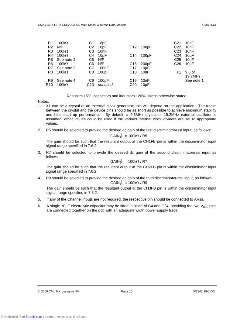
R1 100kΩ C1 18pF C21 10nF R2 N/F C2 18pF C12 100pF C22 10nF R3 100kΩ C3 10nF C23 10nF R4 100kΩ C4 10µF C14 100pF C24 10µF R5 See note 2 C5 N/F C25 10nF R6 100kΩ C6 N/F C16 200pF C26 10µF R7 See note 3 C7 100nF C17 10µF R8 100kΩ C8 100pF C18 10nF X1 9.6 or
19.2MHz R9 See note 4 C9 100pF C19 10nF See note 1
R10 100kΩ C10 not used C20 10µF
Resistors ±5%, capacitors and inductors ±20% unless otherwise stated. Notes: 1. X1 can be a crystal or an external clock generator; this will depend on the application. The tracks
between the crystal and the device pins should be as short as possible to achieve maximum stability and best start up performance. By default, a 9.6MHz crystal or 19.2MHz external oscillator is assumed, other values could be used if the various internal clock dividers are set to appropriate values.
2. R5 should be selected to provide the desired dc gain of the first discriminator/rssi input, as follows: ⏐ GAIN1⏐ = 100kΩ / R5
The gain should be such that the resultant output at the CH1FB pin is within the discriminator input signal range specified in 7.6.2.
3. R7 should be selected to provide the desired dc gain of the second discriminator/rssi input as follows:
⏐ GAIN2⏐ = 100kΩ / R7 The gain should be such that the resultant output at the CH2FB pin is within the discriminator input signal range specified in 7.6.2.
4. R9 should be selected to provide the desired dc gain of the third discriminator/rssi input, as follows: ⏐ GAIN3⏐ = 100kΩ / R9
The gain should be such that the resultant output at the CH3FB pin is within the discriminator input signal range specified in 7.6.2.
5. If any of the Channel inputs are not required, the respective pin should be connected to AVss.
6. A single 10µF electrolytic capacitor may be fitted in place of C4 and C24, providing the two VDEC pins are connected together on the pcb with an adequate width power supply trace.
Downloaded from Elcodis.com electronic components distributor

CMX7143 FI-1.0: GMSK/GFSK Multi-Mode Wireless Data Modem CMX7143
© 2008 CML Microsystems Plc Page 11 D/7143_FI-1.0/3
5 PCB Layout Guidelines and Power Supply Decoupling
Figure 3 CMX7143 Power Supply and De-coupling
Component Values as per Figure 2. Notes:
It is important to protect the analogue pins from extraneous in-band noise and to minimise the impedance between the CMX7143 and the supply and bias de-coupling capacitors. The de-coupling capacitors C3, C7, C18, C19, C21, C22, C24 and C25 should be as close as possible to the CMX7143. It is therefore recommended that the printed circuit board is laid out with separate ground planes for the AVSS and DVSS supplies in the area of the CMX7143, with provision to make links between them, close to the CMX7143. Use of a multi-layer printed circuit board will facilitate the provision of ground planes on separate layers.
VBIAS is used as an internal reference for detecting and generating the various analogue signals. It must be carefully decoupled, to ensure its integrity, so apart from the decoupling capacitor shown, no other loads should be connected. If VBIAS needs to be used to set the discriminator mid-point reference, it must be buffered with a high input impedance buffer.
The crystal, X1, may be replaced with an external clock source.
Downloaded from Elcodis.com electronic components distributor
CMX7143 FI-1.0: GMSK/GFSK Multi-Mode Wireless Data Modem CMX7143
© 2008 CML Microsystems Plc Page 12 D/7143_FI-1.0/3
6 General Description 6.1 CMX7143 Features The CMX7143 is intended for use in half duplex modems. A flexible power control facility allows the device to be placed in its optimum powersave mode when not actively processing signals.
The device includes a crystal clock generator, with buffered output, to provide a common system clock if required.
A block diagram of the device is shown in Figure 1.
Input to the RxSig and RSSI/CS signal processing blocks can be routed from any of the three RxSig/RSSI channel input pins (CH1N, CH2N or CH3N).
Tx Functions: o Flexible Tx data transfer block size, up to 104bits o Automatic Preamble, Frame Sync insertion simplifies host control o Modulator producing 2 point or I/Q outputs with programmable deviation o Data pulse shape filtering o RAMDAC capability for PA ramping control o Tx trigger feature allowing precise control of burst start time o Tx burst sequence for automatic RAMDAC ramp and Tx hardware switching o Carrier sense for “listen before talk” operation o Raw and Formatted (Channel coded) data modes
Rx Functions:
o Demodulator input with input amplifier and programmable gain adjustment o Flexible Rx data transfer block size, up to 104bits o Automatic Frame Sync detection simplifies host control o Rx filtering o Tracking of symbol timing and received signal levels o Raw and Formatted (Channel coded) data modes
Auxiliary Functions:
o 2 programmable system clock outputs o 2 auxiliary ADCs with four selectable input paths o 4 auxiliary DACs, one with built-in programmable RAMDAC
Interface:
o Optimised C-BUS (4 wire high speed synchronous serial command / data bus) interface to host for control and data transfer
o Open drain IRQ to host o Four GPIO pins o Tx trigger input (Provided by GPIO1) o Flash/EEPROM boot mode o C-BUS (host) boot mode
While in idle mode the AuxADC can be used to detect the RSSI signal from the RF section, while still retaining a significant degree of power saving within the CMX7143 and obviating the need to wake the host up un-necessarily. The use of the programmable thresholds allows for user selection of wake up threshold programmed from the host.
In carrier sense mode RSSI will be sampled using the selected RxSig/RSSI input, and averaged automatically by the CMX7143, resulting in a decision to transmit or not, based on the presence of a signal on the channel.
Downloaded from Elcodis.com electronic components distributor
CMX7143 FI-1.0: GMSK/GFSK Multi-Mode Wireless Data Modem CMX7143
© 2008 CML Microsystems Plc Page 13 D/7143_FI-1.0/3
Both transmit and receive data can be raw or in the form of coded data blocks. Coding is compatible with the FX909B and MX909B.
7 Detailed Descriptions 7.1 Xtal Frequency The CMX7143 is designed to work with a Xtal with frequency 9.6MHz, or external frequency oscillator of 9.6 or 19.2MHz. Program Register Block 3 (see User Manual) must be loaded with the correct values to ensure that the device will work to specification with the user selected clock frequency. A table of configuration values can be found in Table 5, they support configuration at baud rates of 4k to 20k symbols per second (4k to 20kbps) using either crystal frequency. Rates other than those tabulated (within this range) should be possible, further information can be provided on request.
7.2 Host Interface A serial data interface (C-BUS) is used for command, status and data transfers between the CMX7143 and the host µC; this interface is compatible with Microwire™, SPI™1 and other similar interfaces. Interrupt signals notify the host µC when a change in status has occurred and the µC should read the status register across the C-BUS and respond accordingly. Interrupts only occur if the appropriate mask bit has been set, see Interrupt Operation.
7.2.1 C-BUS Operation This block provides for the transfer of data and control or status information between the CMX7143’s internal registers and the host µC over the C-BUS serial interface. Each transaction consists of a single Address byte sent from the µC which may be followed by one or more Data byte(s) sent from the µC to be written into one of the CMX7143’s Write Only Registers, or one or more data byte(s) read out from one of the CMX7143’s Read Only Registers, as illustrated in Figure 4.
Data sent from the µC on the Command Data line is clocked into the CMX7143 on the rising edge of the Serial Clock input. Reply Data sent from the CMX7143 to the µC is valid when the Serial Clock is high. The CSN line must be held low during a data transfer and kept high between transfers. The C-BUS interface is compatible with most common µC serial interfaces and may also be easily implemented with general purpose µC I/O pins controlled by a simple software routine.
The number of data bytes following an Address byte is dependent on the value of the Address byte. The most significant bit of the address or data are sent first. For detailed timings see section 0. Note that, due to internal timing constraints, there may be a delay of up to 250μs between the end of a C-BUS write operation and the device reading the data from its internal register.
1 Microwire™ is a trademark of National Semiconductors, SPI™ is a trademark of Motorola
Downloaded from Elcodis.com electronic components distributor

CMX7143 FI-1.0: GMSK/GFSK Multi-Mode Wireless Data Modem CMX7143
© 2008 CML Microsystems Plc Page 14 D/7143_FI-1.0/3
C-BUS Write:
See Note 1 See Note 2 CSN Serial_Clock CMD_DATA 7 6 5 4 3 2 1 0 7 6 … 0 7 … 0 MSB LSB MSB LSB MSB LSB
Address / Command byte Upper 8 bits Lower 8 bits
REPLY_DATA
High Z state C-BUS Read:
See Note 2 CSN Serial_Clock CMD_DATA 7 6 5 4 3 2 1 0 MSB LSB
Address byte Upper 8 bits Lower 8 bits
REPLY_DATA 7 6 … 0 7 … 0
High Z state MSB LSB MSB LSB
Data value unimportant
Repeated cycles
Either logic level valid (and may change)
Either logic level valid (but must not change from low to high)
Figure 4 C-BUS Transactions Notes:
1. For Command byte transfers only the first 8 bits are transferred ($01 = Reset). 2. For single byte data transfers only the first 8 bits of the data are transferred. 3. The CMD_DATA and REPLY_DATA lines are never active at the same time. The Address byte
determines the data direction for each C-BUS transfer. 4. The Serial_Clock input can be high or low at the start and end of each C-BUS transaction. 5. The gaps shown between each byte on the CMD_DATA and REPLY_DATA lines in the above
diagram are optional, the host may insert gaps or concatenate the data as required.
Downloaded from Elcodis.com electronic components distributor

CMX7143 FI-1.0: GMSK/GFSK Multi-Mode Wireless Data Modem CMX7143
© 2008 CML Microsystems Plc Page 15 D/7143_FI-1.0/3
7.3 Function Image™ Loading The Function Image™ (FI), which defines the operational capabilities of the device, may be obtained from the CML Technical Portal, following registration. This is in the form of a 'C' header file which can be included into the host controller software or programmed into an external EEPROM or Flash memory. The maximum possible size of Function ImageTM is 46 kbytes, although a typical FI will be less than this. Note that the BOOTEN pins are only read at power-on or following a C-BUS General Reset and must remain stable throughout the FI loading process. Once the FI load has completed, the BOOTEN pins are ignored by the CMX7143 until the next power-up or C-BUS General Reset. The BOOTEN pins are both fitted with internal low-current pulldown devices.
For C-BUS load operation, both pins should be pulled high by connecting them to DVDD either directly or via a 47k resistor (see Table 1).
For Flash/EEPROM load, only BOOTEN1 needs to be pulled high in a similar manner, however, if it is required to program the EEPROM or Flash memory in-situ from the host, either a jumper to DVDD or a link to a host I/O pin should be provided to pull BOOTEN2 high when required (see Table 1).
Once the FI has been loaded, the CMX7143 performs these actions:-
(1) the product identification code ($7143) is reported in C-BUS register $C5 (2) the FI version code is reported in C-BUS register $C9 (3) the two 32-bit FI checksums are reported in C-BUS register pairs $A9, $AA and $B8, $B9 (4) the device waits for the host to load the 32-bit Device Activation Code to C-BUS register $C8 (5) once activated, the device initialises fully, enters idle mode and becomes ready for use.
The checksums can be verified against the published values to ensure that the FI has loaded correctly. Once the FI has been activated, the checksum, product identification and version code registers are cleared and these values are no longer available. If an invalid activation code is loaded, the device will report the value $DEAD in register $A9 and become unresponsive to all further host commands (including General Reset). Both the Device Activation Code and the checksum values are available from the CML Technical Portal.
Table 1 BOOTEN Pin States BOOTEN2 BOOTEN1 C-BUS Host load 1 1 reserved 1 0 Flash/EEPROM load 0 1 No FI load 0 0
Note: In the rare event that a General Reset needs to be issued without the requirement to re-load the FI, the
BOOTEN pins must both be cleared to '0' before issuing the Reset command. The Checksum values will be reported and the Device Activation code will need to be sent in a similar manner as that shown in Figure 6. There will not be any FI loading delay. This assumes that a valid FI has been previously loaded and that Vdd has been maintained throughout the reset to preserve the data.
Downloaded from Elcodis.com electronic components distributor
CMX7143 FI-1.0: GMSK/GFSK Multi-Mode Wireless Data Modem CMX7143
© 2008 CML Microsystems Plc Page 16 D/7143_FI-1.0/3
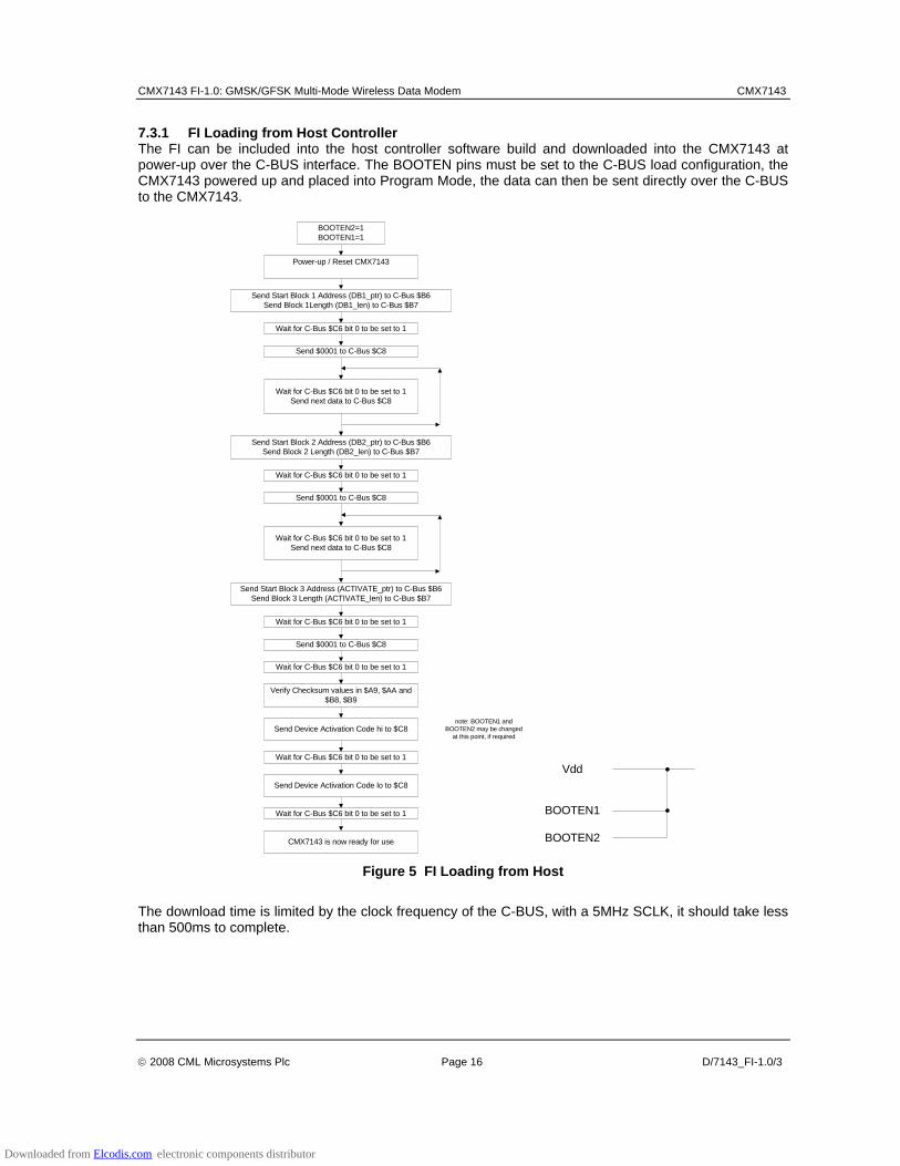
7.3.1 FI Loading from Host Controller The FI can be included into the host controller software build and downloaded into the CMX7143 at power-up over the C-BUS interface. The BOOTEN pins must be set to the C-BUS load configuration, the CMX7143 powered up and placed into Program Mode, the data can then be sent directly over the C-BUS to the CMX7143.
BOOTEN2=1BOOTEN1=1
Power-up / Reset CMX7143
Send Start Block 1 Address (DB1_ptr) to C-Bus $B6Send Block 1Length (DB1_len) to C-Bus $B7
Wait for C-Bus $C6 bit 0 to be set to 1Send next data to C-Bus $C8
Verify Checksum values in $A9, $AA and $B8, $B9
Send Device Activation Code hi to $C8
Send Device Activation Code lo to $C8
Wait for C-Bus $C6 bit 0 to be set to 1
CMX7143 is now ready for use
Send Start Block 2 Address (DB2_ptr) to C-Bus $B6Send Block 2 Length (DB2_len) to C-Bus $B7
Wait for C-Bus $C6 bit 0 to be set to 1Send next data to C-Bus $C8
Wait for C-Bus $C6 bit 0 to be set to 1
Send Start Block 3 Address (ACTIVATE_ptr) to C-Bus $B6Send Block 3 Length (ACTIVATE_len) to C-Bus $B7
Wait for C-Bus $C6 bit 0 to be set to 1
Send $0001 to C-Bus $C8
Wait for C-Bus $C6 bit 0 to be set to 1
Send $0001 to C-Bus $C8
Wait for C-Bus $C6 bit 0 to be set to 1
Send $0001 to C-Bus $C8
Wait for C-Bus $C6 bit 0 to be set to 1
note: BOOTEN1 and BOOTEN2 may be changed
at this point, if required
BOOTEN1
BOOTEN2
Vdd
Figure 5 FI Loading from Host
The download time is limited by the clock frequency of the C-BUS, with a 5MHz SCLK, it should take less than 500ms to complete.
Downloaded from Elcodis.com electronic components distributor
CMX7143 FI-1.0: GMSK/GFSK Multi-Mode Wireless Data Modem CMX7143
© 2008 CML Microsystems Plc Page 17 D/7143_FI-1.0/3
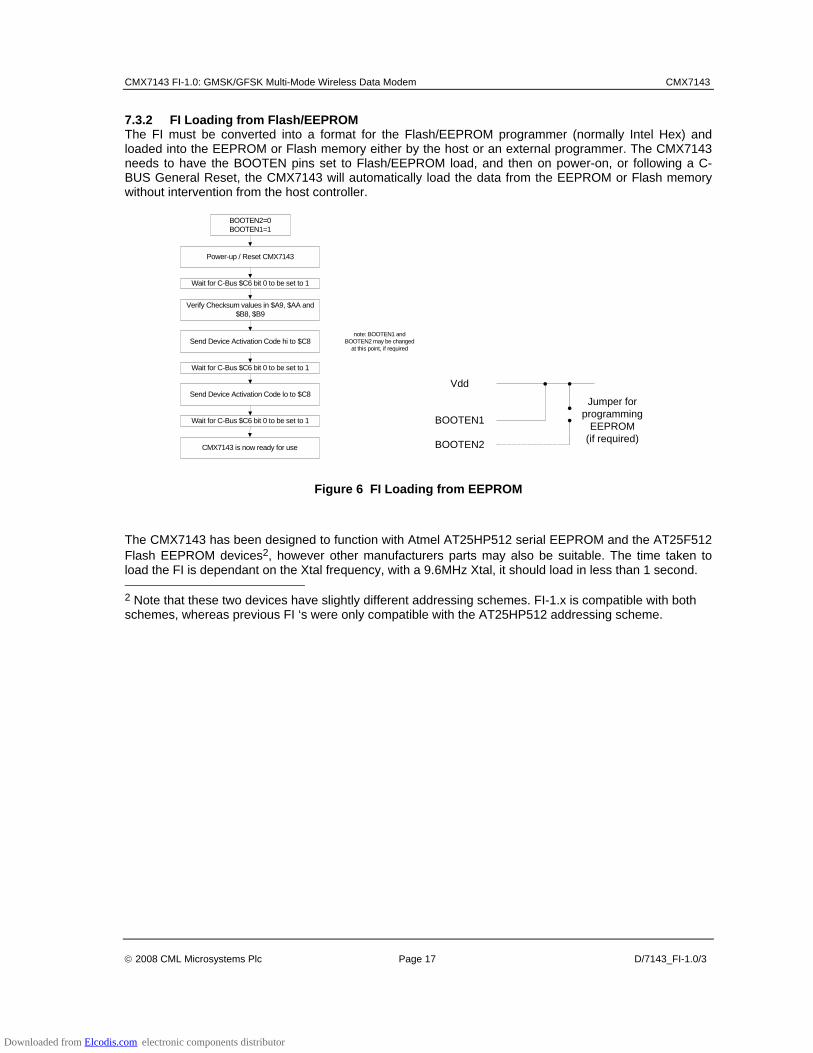
7.3.2 FI Loading from Flash/EEPROM The FI must be converted into a format for the Flash/EEPROM programmer (normally Intel Hex) and loaded into the EEPROM or Flash memory either by the host or an external programmer. The CMX7143 needs to have the BOOTEN pins set to Flash/EEPROM load, and then on power-on, or following a C-BUS General Reset, the CMX7143 will automatically load the data from the EEPROM or Flash memory without intervention from the host controller.
BOOTEN2=0BOOTEN1=1
Power-up / Reset CMX7143
Verify Checksum values in $A9, $AA and $B8, $B9
Send Device Activation Code hi to $C8
Send Device Activation Code lo to $C8
Wait for C-Bus $C6 bit 0 to be set to 1
CMX7143 is now ready for use
Wait for C-Bus $C6 bit 0 to be set to 1
Wait for C-Bus $C6 bit 0 to be set to 1
note: BOOTEN1 and BOOTEN2 may be changed
at this point, if required
BOOTEN1
BOOTEN2
Vdd
Jumper for programming
EEPROM (if required)
Figure 6 FI Loading from EEPROM
The CMX7143 has been designed to function with Atmel AT25HP512 serial EEPROM and the AT25F512 Flash EEPROM devices2, however other manufacturers parts may also be suitable. The time taken to load the FI is dependant on the Xtal frequency, with a 9.6MHz Xtal, it should load in less than 1 second. 2 Note that these two devices have slightly different addressing schemes. FI-1.x is compatible with both schemes, whereas previous FI ‘s were only compatible with the AT25HP512 addressing scheme.
Downloaded from Elcodis.com electronic components distributor

CMX7143 FI-1.0: GMSK/GFSK Multi-Mode Wireless Data Modem CMX7143
© 2008 CML Microsystems Plc Page 18 D/7143_FI-1.0/3
7.4 Device Control Once the Function Image is loaded the CMX7143 can be set into one of four main modes using the Modem Mode and Control - $C1 write register:
• Idle mode – for configuration or low power operation • Transmit mode – for transmission of raw or formatted data • Receive mode – for detection and reception of bursts containing raw or formatted data • Carrier sense mode – for attempting to transmit if the channel is free, otherwise continuing to
receive
These four modes are described in the following sections. All control is carried out over the C-BUS interface: either directly to operational registers in transmit, receive and carrier sense modes or, for parameters that are not likely to change during operation, using the Programming register ($C8) in idle mode.
To conserve power when the device is not actively processing a signal, place the device into Idle mode. Additional Power-saving can be achieved by disabling the unused hardware blocks, however, care must be taken not to disturb any sections that are automatically controlled. Note that the BIAS block must be enabled to allow any of the Input or Output blocks to function. It is only possible to write to the Programming register whilst in IDLE mode. See:
o Power Down Control - $C0 write o Modem Mode and Control - $C1 write o Programming Register – $C8 write
7.4.1 Normal Operation Overview In normal operation (after the CMX7143 is configured) the appropriate mode must be selected and data provided in transmit or retrieved in receive. This process is carried out by selecting the mode (Tx, Rx or Carrier Sense), frame sync 1 or 2 and formatted or raw data. Such a selection is required at the beginning of transmission or reception of a burst.
In transmit (or following a carrier sense period where no signal is detected on channel) the CMX7143 will begin by switching GPIO signals as configured by the transmit sequence. The RAMDAC can also be configured to ramp up at this point. Transmission then begins with preamble and the selected framesync. The main payload of user data comes next, ending with selectable tail bits. The burst ends with the transmission sequence ramping the RAMDAC down and/or switching GPIO signals.
In receive (or following a carrier sense period where signal is detected on channel) the CMX7143 will begin by searching for either or both of the configured frame sync patterns. On detection of a frame sync reception and data output will begin. Reception continues until the CMX7143 is switched into a different mode, determined by the host.
During the burst data blocks must be transferred into or out of the CMX7143. Each of these transfers uses the RxData or TxData registers to transfer data and the status register to indicate that the data has been dealt with successfully. Each transfer can contain a host selectable number of bits or bytes. The CMX7143 can be configured to interrupt the host on completion of a data transfer.
The CMX7143 offers internal buffering of data in addition to the RxData and TxData registers in both receive and transmit directions. The amount of buffering offered is dependant on the mode in which the device is operating and the size of any transfers carried out by the host. In the process of burst transmission or reception the most significant registers are:
o Modem Mode and Control - $C1 write o Status - $C6 read o Interrupt Mask - $CE write o RxControl - $C3 write o RxData0 - $B8 read (Plus RxData1-6) containing control fields and data o TxData0 - $B5 write (Plus TxData1-6)containing control fields and data
Downloaded from Elcodis.com electronic components distributor

CMX7143 FI-1.0: GMSK/GFSK Multi-Mode Wireless Data Modem CMX7143
© 2008 CML Microsystems Plc Page 19 D/7143_FI-1.0/3
7.4.2 Device Configuration (Using the Programming Register) While in idle mode the programming register becomes active. The programming register provides access to the programming blocks. Programming blocks each allow for configuration of the CMX7143 on power up and during major mode change. Features that can be configured include;
• Flexible selection of Baud rates, from 4k to 20k baud. • Pre-amble and frame syncs to be using in transmit and receive • Selection of Automatic control of GPIO1-4 and the RAMDAC during transmission • Configuration of RAMDAC profile • Configuration of AuxADC and RSSI averaging • Programming of input and output gains and offsets. • Configuration of the carrier sense window and thresholds
Full details of how to configure these aspects of device operation are given in section 10.2 in the User Manual.
7.4.3 Device Configuration (Using dedicated registers) Some device features may be configured using dedicated registers. This allows for configuration outside of idle mode. Configuration of the following features is possible:
• Auxiliary ADC detect thresholds • Auxiliary ADC input selection and averaging mode • Power down control • Input gain and input/output signal routing
The registers that allow configuration of these features are:
o Aux config - $A7 write o AuxConfig2 - $CD write o Power Down Control - $C0 write o AuxConfig2 - $CD write o Input Gain and Input/Output Signal Routing - $B1 write
7.4.4 Interrupt Operation The CMX7143 can produce an interrupt output when various events occur. Possible events include detection of a frame sync or an overflow of the internal data buffering in receive, or completion of transmission whilst in transmit.
Each event has an associated status register bit and an interrupt mask register bit. The interrupt mask register is used to select which status events will trigger an interrupt on the IRQN line. Events can all be masked using the IRQ mask bit (bit 15) or individually masked using the interrupt mask register. Enabling an interrupt by setting a mask bit (0→1) after the corresponding Status register bit has already been set to 1 will also cause the an interrupt on the IRQN line. The IRQ bit (bit 15) of the status register reflects the IRQN line state.
All interrupt flag bits in the Status register, except the Programming Flag (bit 0), are cleared and the interrupt request is cleared following the command/address phase of a C-BUS read of the Status register. See:
o Interrupt Mask - $CE write o Status - $C6 read
Downloaded from Elcodis.com electronic components distributor
CMX7143 FI-1.0: GMSK/GFSK Multi-Mode Wireless Data Modem CMX7143
© 2008 CML Microsystems Plc Page 20 D/7143_FI-1.0/3
7.4.5 Signal Routing The CMX7143 offers a flexible routing architecture, with three signal inputs, and two modulator outputs. The analogue gain / attenuation of each input and output can be set individually, with additional Fine Attenuation control available via the Programming registers.
One of the three input sources (CH1N, CH2N or CH3N) should be routed to RxSigIn and another to RSSI In. Output 1 and 2 should be routed to MOD1 and MOD2 as required. The input source routed to RxSigIn will be treated as the input signal to demodulate. This is expected to be the demod output from a limiter discriminator. The input source routed to RSSI will be averaged and the result presented in the Aux Data Registers. If carrier sense is selected then the same input source will be averaged over a short period internally in order to make the decision on whether to transmit or not. The output signals MOD1 and MOD2 will provide 2 point modulation outputs with independently programmable gains. Alternatively an I,Q output may be selected in which case MOD1 and MOD2 will provide in phase and quadrature signals. See:
o Input Gain and Input/Output Signal Routing - $B1 write o AuxConfig2 - $CD write
7.4.6 Tx Mode In typical Tx operation, the preamble and FS1 or FS2 are transmitted automatically (default values may be changed by use of the Program Registers), and then data from the TxData Block is transmitted directly until the Mode is changed to Rx or Idle. The first block of data MUST be loaded into the TxData registers BEFORE executing the Modem Mode change to Tx.
The host should write the initial data to the C-BUS TxData registers and then set modem control to the required transmit type with the Mode bits as Tx. As soon as the data has been read from the C-BUS TxData registers the DataRDY IRQ will be asserted (when configured correctly). More data should be loaded into the TxData registers at this stage before data buffered in the CMX7143 runs out, otherwise the burst will end.
For precise control of the instant that transmission starts it is possible to trigger a transmission using GPIO1 as an input. In addition to triggering the modulation output, it is possible to define a transmission sequence with defined RAMDAC ramp up/down, and GPIO on/off events. The transmission sequence is configured using Program Block 1. Selecting a Tx mode with GPIO1 configured as an “automatic input” places the device into a “Tx pending” state, where it is neither receiving nor transmitting, just waiting for a trigger on GPIO1 to begin transmission.
In general Figure 7 Host Tx Data Flow (No Tx sequence/Carrier sense) can be extended to represent operation when a transmit sequence is defined by the host by:
• Removing the need for the host to provide a ramp up – instead the configured Tx sequence will deal with this.
• Inserting GPIO on/off events before ramp up and after ramp down as specified by the transmit sequence.
Downloaded from Elcodis.com electronic components distributor

CMX7143 FI-1.0: GMSK/GFSK Multi-Mode Wireless Data Modem CMX7143
© 2008 CML Microsystems Plc Page 21 D/7143_FI-1.0/3
Load data to C-Bus TxDataBlocktransaction count =0, byte/bit count or block type as required
Set Modem Control toTxPreamble, Frame sync and required data mode, Mode = Tx
IRQ = DataRdy?
No
The Modem will transmit the preamble, frame sync and data The host should ensure that any external hardware is also set into Tx
mode (if not automatically controlled by the GPIO pins).
note:
yes
more data to send?
Load data to C-Bus TxDataBlock
transaction count++, byte/bit count as required.
yesNo
See Rx_Process flow diagramnote:
Set Modem Control to Idle: Mode = Idle
The host should ensure that any external hardware is also set into Idle mode (if not
automatically controlled by the GPIO pins).note:
Goto Rx_Process
Goto Idle Mode
This assumes that:The transmit control sequence and frame syncs have been configured using the programming register
note:
Tx_Process
IRQ = TxDone?
No
Yes
IRQ=Error, Modem status = Underflow may occur at
this point, if enabled. note:
Due to internal processing delays in the filters etc, the Host should wait for IRQ=TxDone or implement its own delay to ensure all data has been transmitted.
note:
Execute RAMDAC rampdown
Execute RAMDAC rampup
No
Ensure that RAMDAC speed is fast enough to allow for
hardware and internal processing delays
note:
Tx triggered on GPIO?
GPIO Tx Trigger
Here the device is waiting for a GPIO trigger to start the
transmission attempt. As no carrier sense is selected it is
not receiving and is committed to transmit
note:Wait for Tx TriggerYes
Yes
Figure 7 Host Tx Data Flow (No Tx sequence/Carrier sense)
Downloaded from Elcodis.com electronic components distributor

CMX7143 FI-1.0: GMSK/GFSK Multi-Mode Wireless Data Modem CMX7143
© 2008 CML Microsystems Plc Page 22 D/7143_FI-1.0/3
7.4.7 Rx Mode
In Rx mode a frame sync must be detected, then data is supplied to the host through the RxData registers and should be read in response to a DataRDY IRQ (when configured). The CMX7143 will continue decoding the input waveform until the host sets the Mode bits to either Tx or IDLE, as required. A test mode to examine the Rx “EYE” is also provided.
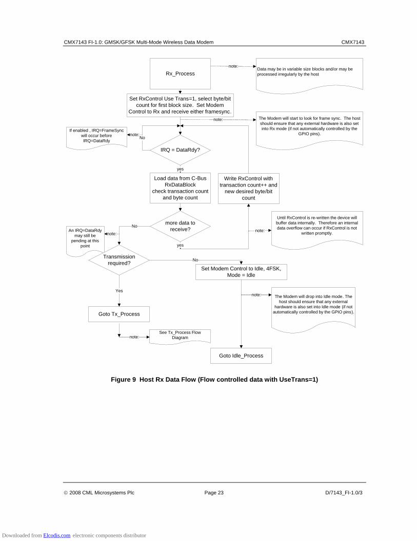
Once initial timing is established, timing corrections can be derived from the data to track the received signal. The Modem control register allows selection of the tracking mode used to track both the signal level and symbol timing of the input signal. It is recommended that the automatic modes are used. If the UseTrans bit in the RxControl register is set to 0 the device will update the C-BUS RxData registers with payload data as it becomes available and the host MUST respond to the DataRDY IRQ before the data is over-written by the modem. If UseTrans is set to 1 then the host can use the transaction counter in the RxControl register to control the data read transaction rate.
Rx_Process
Set RxControl Use Trans=0, select byte count for block size. Set Modem Control to
Rx and receive either framesync.
IRQ = DataRdy?
No
The Modem will start to look for frame sync. The host should ensure that any external hardware is also set into Rx mode (if not
automatically controlled by the GPIO pins).
note:
yes
more data to receive?
Load data from C-Bus RxDataBlock
check transaction count and byte count
yes
No
See Tx_Process Flow Diagramnote:
Set Modem Control to Idle, 4FSK, Mode = Idle
The Modem will drop into Idle mode. The host should ensure that any external
hardware is also set into Idle mode (if not automatically controlled by the GPIO pins).
note:
No
Goto Tx_Process
Goto Idle_Process
This assumes that:Data is in fixed size byte blocks and will be processed regularly by the host
note:
Yes
If enabled , IRQ=FrameSync will occur before IRQ=DataRdy
note:
An IRQ=DataRdy may still be
pending at this point
note:
Transmission required?
Figure 8 Host Rx Data Flow (Use Trans=0)
Downloaded from Elcodis.com electronic components distributor
CMX7143 FI-1.0: GMSK/GFSK Multi-Mode Wireless Data Modem CMX7143
© 2008 CML Microsystems Plc Page 23 D/7143_FI-1.0/3
Rx_Process
Set RxControl Use Trans=1, select byte/bit count for first block size. Set Modem
Control to Rx and receive either framesync.
IRQ = DataRdy?
No
The Modem will start to look for frame sync. The host should ensure that any external hardware is also set into Rx mode (if not automatically controlled by the
GPIO pins).
note:
yes
more data to receive?
Load data from C-Bus RxDataBlock
check transaction count and byte count
yes
No
See Tx_Process Flow Diagramnote:
Set Modem Control to Idle, 4FSK, Mode = Idle
The Modem will drop into Idle mode. The host should ensure that any external
hardware is also set into Idle mode (if not automatically controlled by the GPIO pins).
note:
No
Goto Tx_Process
Goto Idle_Process
Data may be in variable size blocks and/or may be processed irregularly by the host
note:
If enabled , IRQ=FrameSync will occur before IRQ=DataRdy
note:
An IRQ=DataRdy may still be
pending at this point
note:
Write RxControl with transaction count++ and
new desired byte/bit count
Until RxControl is re-written the device will buffer data internally. Therefore an internal data overflow can occur if RxControl is not
written promptly.note:
Transmission required?
Yes
Figure 9 Host Rx Data Flow (Flow controlled data with UseTrans=1)
Downloaded from Elcodis.com electronic components distributor

CMX7143 FI-1.0: GMSK/GFSK Multi-Mode Wireless Data Modem CMX7143
© 2008 CML Microsystems Plc Page 24 D/7143_FI-1.0/3
7.4.8 Carrier Sense mode Carrier sense mode is a receive mode, pending a transmission. A carrier sense period, averaging window length and threshold must be defined using the programming register prior to entering this mode. For this mode to operate correctly an RSSI signal must be connected to the RSSI/carrier sense input. On entry to Carrier sense mode reception will begin (or continue if the previous mode was receive) with an attempt to search for a frame sync. During the defined carrier sense period average RSSI will be computed over a moving window. Three outcomes are possible:
1. If during the carrier sense period the average RSSI is above the carrier sense threshold then transmission will be aborted, and search for frame sync will continue. The device reverts to receive.
2. There is a possibility that a valid frame sync will be detected during the carrier sense period. If this is the case, the transmission will be aborted immediately and the device reverts to receive.
3. If the RSSI average remains below the carrier sense threshold then transmission will proceed.
In each of the three possible cases, status bits will be used to indicate the result of the carrier sense period. If the carrier sense mechanism is used in conjunction with GPIO1 as a Tx trigger operation is as follows: The device is put in receive, searching for a frame sync. If frame sync is found during this period then it is indicated to the host via the status bits and normal reception resumes. No carrier sense happens until GPIO1 is used to start the transmit process, at which point carrier sense begins and operation is as described above.
Downloaded from Elcodis.com electronic components distributor

CMX7143 FI-1.0: GMSK/GFSK Multi-Mode Wireless Data Modem CMX7143
© 2008 CML Microsystems Plc Page 25 D/7143_FI-1.0/3
Load data to C-Bus TxDataBlock
transaction count =0, byte count as required
Set Modem Control toTxPreamble, Frame sync and required data type, Mode = Carrier Sense
IRQ = FS1 or FS2
No
IRQ=CS abort
No
Yes
This assumes that:A carrier sense threshold and period have been defined using the programming register
note:
Carrier sense process
IRQ = CS TxYes
Ready CBUS RxControl for Rx data transfer in case of carrier being
sensed
Here the device is in receive and searching for a frame
sync, as well as monitoring RSSI (Carrier sensing)
note:
Rx Process
Yes
Tx Process
Tx triggered on GPIO?
No
Yes
IRQ = FS1 or FS2
Rx Process
GPIO Tx Trigger
Carrier sense begins
Here the device is in receive and searching for a frame
sync, as well as waiting for a GPIO trigger to start the
transmission attempt
note:Wait for Tx Trigger
YesYes
Figure 10 Carrier sense
Downloaded from Elcodis.com electronic components distributor
CMX7143 FI-1.0: GMSK/GFSK Multi-Mode Wireless Data Modem CMX7143
© 2008 CML Microsystems Plc Page 26 D/7143_FI-1.0/3
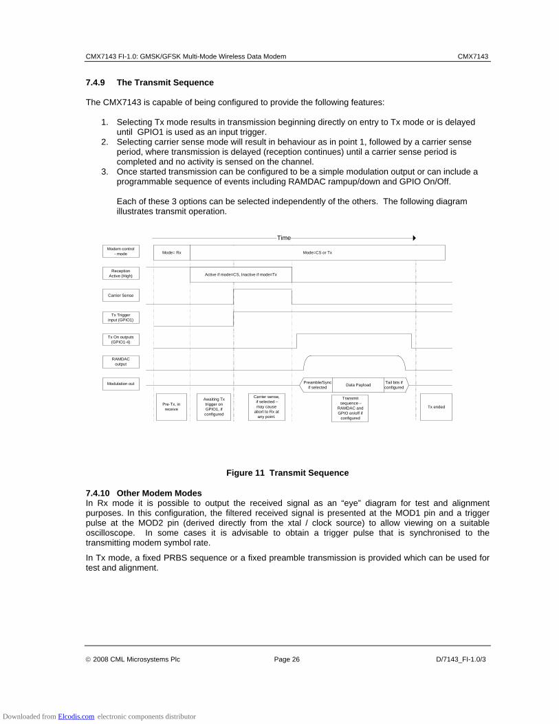
7.4.9 The Transmit Sequence
The CMX7143 is capable of being configured to provide the following features:
1. Selecting Tx mode results in transmission beginning directly on entry to Tx mode or is delayed until GPIO1 is used as an input trigger.
2. Selecting carrier sense mode will result in behaviour as in point 1, followed by a carrier sense period, where transmission is delayed (reception continues) until a carrier sense period is completed and no activity is sensed on the channel.
3. Once started transmission can be configured to be a simple modulation output or can include a programmable sequence of events including RAMDAC rampup/down and GPIO On/Off. Each of these 3 options can be selected independently of the others. The following diagram illustrates transmit operation.
Tail bits if configured
Preamble/Sync if selected
Modem control - mode
Reception Active (High)
RAMDAC output
Carrier Sense
Tx Trigger input (GPIO1)
Tx On outputs (GPIO1-4)
Time
Pre-Tx, in receive
Awaiting Tx trigger on GPIO1, if
configured
Carrier sense, if selected –may cause
abort to Rx at any point.
Transmit sequence –
RAMDAC and GPIO on/off if
configured
Tx ended
Modulation out
Active if mode=CS, Inactive if mode=Tx
Data Payload
Mode= Rx Mode=CS or Tx
Figure 11 Transmit Sequence
7.4.10 Other Modem Modes In Rx mode it is possible to output the received signal as an “eye” diagram for test and alignment purposes. In this configuration, the filtered received signal is presented at the MOD1 pin and a trigger pulse at the MOD2 pin (derived directly from the xtal / clock source) to allow viewing on a suitable oscilloscope. In some cases it is advisable to obtain a trigger pulse that is synchronised to the transmitting modem symbol rate.
In Tx mode, a fixed PRBS sequence or a fixed preamble transmission is provided which can be used for test and alignment.
Downloaded from Elcodis.com electronic components distributor
CMX7143 FI-1.0: GMSK/GFSK Multi-Mode Wireless Data Modem CMX7143
© 2008 CML Microsystems Plc Page 27 D/7143_FI-1.0/3
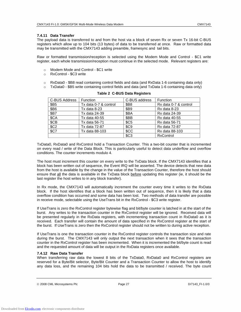
7.4.11 Data Transfer The payload data is transferred to and from the host via a block of seven Rx or seven Tx 16-bit C-BUS registers which allow up to 104 bits (13 bytes) of data to be transferred at once. Raw or formatted data may be transmitted with the CMX7143 adding preamble, framesync and tail bits. Raw or formatted transmission/reception is selected using the Modem Mode and Control - $C1 write register, each whole transmission/reception must continue in the selected mode. Relevant registers are:
o Modem Mode and Control - $C1 write o RxControl - $C3 write
o RxData0 - $B8 read containing control fields and data (and RxData 1-6 containing data only) o TxData0 - $B5 write containing control fields and data (and TxData 1-6 containing data only)
Table 2 C-BUS Data Registers
C-BUS Address Function C-BUS address Function $B5 Tx data 0-7 & control $B8 Rx data 0-7 & control $B6 Tx data 8-23 $B9 Rx data 8-23 $B7 Tx data 24-39 $BA Rx data 24-39 $CA Tx data 40-55 $BB Rx data 40-55 $CB Tx data 56-71 $C5 Rx data 56-71 $C2 Tx data 72-87 $C9 Rx data 72-87 $C7 Tx data 88-103 $CC Rx data 88-103 $C3 RxControl
TxData0, RxData0 and RxControl hold a Transaction Counter. This a two-bit counter that is incremented on every read / write of the Data Block. This is particularly useful to detect data underflow and overflow conditions. The counter increments modulo 4. The host must increment this counter on every write to the TxData block. If the CMX7143 identifies that a block has been written out of sequence, the Event IRQ will be asserted. The device detects that new data from the host is available by the change in the value of the Transaction Counter, therefore the host should ensure that all the data is available in the TxData block before updating this register (ie, it should be the last register the host writes to in any block transfer). In Rx mode, the CMX7143 will automatically increment the counter every time it writes to the RxData block. If the host identifies that a block has been written out of sequence, then it is likely that a data overflow condition has occurred and some data has been lost. Two methods of data transfer are possible in receive mode, selectable using the UseTrans bit in the RxControl - $C3 write register. If UseTrans is zero the RxControl register bytewise flag and bit/byte counter is latched in at the start of the burst. Any writes to the transaction counter in the RxControl register will be ignored. Received data will be presented regularly in the RxData registers, with incrementing transaction count in RxData0 as it is received. Each transfer will contain the amount of data specified in the RxControl register at the start of the burst. If UseTrans is zero then the RxControl register should not be written to during active reception. If UseTrans is one the transaction counter in the RxControl register controls the transaction size and rate during the burst. The CMX7143 will only output the next transaction when it sees that the transaction counter in the RxControl register has been incremented. When it is incremented the bit/byte count is read and the requested amount of data will be output in the RxData registers once available.
7.4.12 Raw Data Transfer When transferring raw data the lowest 8 bits of the TxData0, RxData0 and RxControl registers are reserved for a Byte/Bit selector, Byte/Bit Counter and a Transaction Counter to allow the host to identify any data loss, and the remaining 104 bits hold the data to be transmitted / received. The byte count
Downloaded from Elcodis.com electronic components distributor

CMX7143 FI-1.0: GMSK/GFSK Multi-Mode Wireless Data Modem CMX7143
© 2008 CML Microsystems Plc Page 28 D/7143_FI-1.0/3
indicates how many bytes in the data block are valid and so reduces the need to perform a full 7 word C-BUS read / write if only small blocks of data need to be transferred. The Byte/Bit selector provides a bit transfer mode, which while less efficient (in terms of C-BUS accesses to transfer a quantity of data) provides a facility to transmit or receive a burst of arbitrary length, not just a whole number of bytes. It is suggested that data is transferred in the maximum size blocks possible until the end of a burst - where the remaining bits, or bytes can be transferred in a single transaction of the required size.
7.4.13 Formatted Data Transfer When the transfer of formatted data is selected by the Modem Mode and Control - $C1 write register the TxData0, RxData0 and RxControl registers indicate the block type to use in either sending or decoding the data. The block type dictates the format or quantity of data transferred.
7.4.14 Pre-loading transmit data It is possible to pre-load a number of transactions in to the CMX7143 before transmission begins. To do this the host should load the first transaction into the TxData registers and then select transmit(idle) or carrier sense(idle) mode. The first transaction will be loaded into the CMX7143 but no transmission will begin. Further transactions may be loaded in, creating a larger buffer of data than the TxData registers can hold themselves. Once the buffer is full the CMX7143 will stop accepting transactions. Next, an active Tx mode should be selected by the host and the data in the buffer will be transmitted allowing the host to load further transactions, as the buffer becomes free. Note that in the case of 2-part coded blocks both parts must be loaded into the CMX7143 before any data can be sent. This is due to the way the data is interleaved. It is especially useful to pre-load both haves of any 2-part coded block transmission if the block is to be sent at the beginning of a burst. This is because the CMX7143 will have nothing to send other than the preamble and framesync until both parts of the coded block are loaded in. The buffer of pre-loaded data may be created in carrier sense idle and transmit idle modes simply because in those modes no data is being transmitted - so the buffer does not empty. Transactions and buffering are carried out in an otherwise identical fashion in the active transmit or carrier sense modes. The buffer is cleared when the host changes the lower two bits of the modem control register or following an automatic transition from carrier sense into receive.
7.4.15 Auxiliary clock rates Auxiliary functions including carrier sensing, Aux ADC, DAC and GPIO updates operate on an internal clock. This rate will be referred to in describing these functions. The AuxClk speed is given by: In Idle: AuxClk = Xtal Frequency / (P3.2 x (P3.3 – 128) x 8)
In Tx, if P3.7 less than 256: AuxClk = symbol rate x 5/4 In Tx, if P3.7 more than 256: AuxClk = symbol rate x 5/2 In Rx/CS: AuxClk = symbol rate x 5/4
7.4.16 Auxiliary data The CMX7143 provides 2 auxiliary data registers. These can each be independently configured to output the following information:
• Aux ADC 1 input data and threshold detect status • Aux ADC 2 input data and threshold detect status • The input on GPIO pins 1-4 if configured as inputs • The DC offset of any signal in the process of being received, based on the selected RxSig input • The RSSI of any signal, based on the selected RSSI input
Downloaded from Elcodis.com electronic components distributor

CMX7143 FI-1.0: GMSK/GFSK Multi-Mode Wireless Data Modem CMX7143
© 2008 CML Microsystems Plc Page 29 D/7143_FI-1.0/3
The information is selected using the AuxConfig register. See: o Aux config - $A7 write o Aux data1 - $A9 read o Aux data2 - $AA read
7.4.17 GPIO Pin Operation The CMX7143 provides 4 GPIO pins, each pin can be configured independently as automatic/manual, input/output and rising/falling (with the exception of the combination automatic + input which is only allowed for GPIO1).
Pins that are automatic outputs become part of a transmit sequence and will automatically switch, along with the RAMDAC (if it is configured as automatic) during the course of a burst. Pins that are manual are under direct user control. When automatic a rising, or a falling event at the start or end of transmission will cause the specified GPIO to get switched high or low accordingly.
GPIO1 may be configured as an automatic input. This means that any attempted transmission will wait until GPIO1 input is high (if rising is selected) or low (if falling is selected).
See: o Program Block 1 – Burst Tx Sequence + GPIO configuration o Aux config - $A7 write o Aux data1 - $A9 read o Aux data2 - $AA read o AuxConfig2 - $CD write
7.4.18 Auxiliary ADC Operation The inputs to the two Auxiliary ADCs can be independently routed to any of the Signal Input pins under control of the Signal Routing register, $A7. Conversions will be performed as long as a valid input source is selected, to stop the ADCs, the input source should be set to “off”. BIAS in the Power Down Control - $C0 write register must be enabled for Auxiliary ADC operation.
Averaging can be applied to the ADC readings by selecting the relevant bits in the Signal Routing register, $A7, the length of the averaging is determined by the value in the Programming register (P3.0 and P3.1), and defaults to a value of 0. This is a rolling average system such that a proportion of the current data will be added to the last value. The proportion is determined by the value of the average counter in P3.0 and P3.1. For an average value of 0; 50% of the current value will be applied, for a value of 1 = 25%, 2 = 12.5% etc. The maximum useful value of this field is 8.
High and Low thresholds may be independently applied to both ADC channels (the comparison is applied after averaging, if this is enabled) and an IRQ generated as required (except in the case where the high threshold has been set below the low threshold). The thresholds are programmed via the AuxADC Threshold register, $CD.
Auxiliary ADC data is read back in the AuxADC Data registers ($A9 and $AA) and includes the threshold status as well as the actual conversion data (subject to averaging, if enabled).
The Aux ADC sample rate is affected by settings in Program Block 3 – AuxDAC, RAMDAC and Clock control. The rate will be the AuxClk rate, see 7.4.15 Auxiliary clock rates.
See: o Aux config - $A7 write o Aux data1 - $A9 read o Aux data2 - $AA read o AuxConfig2 - $CD write
Downloaded from Elcodis.com electronic components distributor

CMX7143 FI-1.0: GMSK/GFSK Multi-Mode Wireless Data Modem CMX7143
© 2008 CML Microsystems Plc Page 30 D/7143_FI-1.0/3
7.4.19 Auxiliary DAC / RAMDAC Operation The four Auxiliary DAC channels are programmed via the AuxDAC Control register, $A8. AuxDAC channel 1 may also be programmed to operate as a RAMDAC which will autonomously output a pre-programmed profile at a programmed rate. The RAMDAC may be configured as automatic or manual using Program Block 1 – Burst Tx Sequence + GPIO configuration. The AuxDAC Control register, $A8, with b12 set, controls the RAMDAC mode of operation when configured as a manually triggered RAMDAC.
The default profile is a raised cosine (see Table 6 in the user manual), but this may be over-written with a user defined profile by writing to Program Block 3. The RAMDAC operation is only available in Tx mode and, to avoid glitches in the ramp profile, it is important not to change to IDLE or Rx mode whilst the RAMDAC is still ramping. The AuxDAC outputs hold the user-programmed level during a powersave operation if left enabled, otherwise they will return to zero. Note that access to all four AuxDACs is controlled by the AuxDAC Control register, $A8, and therefore to update all AuxDACs requires four writes to this register. It is not possible to simultaneously update all four AuxDACs.
See: o AuxDAC control / data - $A8 write
Downloaded from Elcodis.com electronic components distributor

CMX7143 FI-1.0: GMSK/GFSK Multi-Mode Wireless Data Modem CMX7143
© 2008 CML Microsystems Plc Page 31 D/7143_FI-1.0/3
7.5 Digital System Clock Generators
Ref CLK div/1 to 512$AC b0-8
PD
VCO
PLL div/1 to 1024$AB b0-9
LPF
SysCLK1Ref
SysCLK1Div
VCO op div/1 to 64
$AB b10-15SysCLK1Pre-CLK
$AC b11-15
SysCLK1Output
384kHz-20MHz
48 - 192kHz(96kHz typ)
SysCLK1 VCO24.576-
98.304MHz(49.152MHz typ)
Ref CLK div/1 to 512$AE b0-8
PD
VCO
PLL div/1 to 1024$AD b0-9
LPF
SysCLK2Ref
SysCLK2Div
VCO op div/1 to 64
$AD b10-15SysCLK2Pre-CLK
$AE b11-15
SysCLK2Output
384kHz-20MHz
48 - 192kHz(96kHz typ)
SysCLK2 VCO24.576-
98.304MHz(49.152MHz typ)
Ref CLK div/1 to 512Prog Reg P3.4 (See
Note)
PD
VCO
PLL div/1 to 1024Prog Reg P3.5 (See
Note)
LPF
MainCLKRef
MainCLKDiv48 - 192kHz
(96kHz typ)
MainCLK VCO24.576-
98.304MHz(49.152MHz typ)
OSC4.0 - 12.288MHz Xtal
or4.0 - 24.576MHZ Clock
Note: MainCLK VCO
And Oscillator used internally.
Controlled by the Programming
Register
Figure 12 Digital Clock Generation Schemes
The CMX7143 includes a 2-pin crystal oscillator circuit. This can either be configured as an oscillator, as shown in section 5, or the XTAL input can be driven by an externally generated clock. The crystal (Xtal) source frequency is expected to be 9.6MHz, if an external oscillator is used the input frequency can be 9.6 or 19.2MHz.
Downloaded from Elcodis.com electronic components distributor

CMX7143 FI-1.0: GMSK/GFSK Multi-Mode Wireless Data Modem CMX7143
© 2008 CML Microsystems Plc Page 32 D/7143_FI-1.0/3
7.5.1 System Clock Operation Two System Clock outputs, SysClock1 Out and SysClock2 Out, are available to drive additional circuits, as required. These are digital phase locked loop (PLL) clocks that can be programmed via the System Clock registers with suitable values chosen by the user. The System Clock PLL Configure registers ($AB and $AD) control the values of the VCO Output divider and Main Divide registers, while the System Clock Ref. Configure registers ($AC and $AE) control the values of the Reference Divider and signal routing configurations. The PLLs are designed for a reference frequency of 96kHz. If not required, these clocks can be independently powersaved. The clock generation scheme is shown in the block diagram of Figure 12. Note that the output is inhibited until enabled by a host command over the C-BUS.
See: o System CLK 1 and 2 PLL data - $AB, $AD write o System CLK 1 and 2 REF - $AC and $AE write
7.5.2 Main Clock Operation A digital PLL is used to create the Main Clock for the internal sections of the CMX7143. The configuration of the main clock and the internal clocks derived from it is controlled using Program Block 3 – AuxDAC, RAMDAC and Clock control.
The CMX7143 defaults to settings appropriate for a 19.2MHz Xtal with a baud rate of 19200s/s, however if a 9.6MHz crystal is to be used, or a different baud rate required then Program Block registers P3.2 to P3.6 will need to be programmed appropriately at power-on. A table of allowed values is provided in Table 5.
It is possible to route the output from the Main clock VCO to the VCO output dividers for either SysCLK1 or SYSCLK2 output frequency generation. However, as the Main clock VCO output is used internally there are constraints on selection of its frequency. The frequency will be based on programming register P3.4 and P3.5, with allowed values given in Table 5 Xtal/Clock Frequency Settings for Program Block 3. Additionally, as the CMX7143 disables the Main clock VCO during idle mode, this selection will only be of use during the active modes of the device.
See: o Program Block 3 – AuxDAC, RAMDAC and Clock control o System CLK 1 and 2 REF - $AC and $AE write o Table 5 Xtal/Clock Frequency Settings for Program Block 3
7.6 Signal Level Optimisation The internal signal processing of the CMX7143 will operate with wide dynamic range and low distortion only if the signal level at all stages in the signal processing chain is kept within the recommended limits. For a device working from a 3.3V ±10% supply, the maximum signal level which can be accommodated without distortion is [(3.3 x 90%) - (2 x 0.3V)] Volts pk-pk = 838mV rms, assuming a sine wave signal. This should not be exceeded at any stage.
7.6.1 Transmit Path Levels For the maximum signal out of the MOD1 and MOD2 attenuators, the signal level at the output of the Modem block is set to be 0dB, The Fine Output adjustment has a maximum attenuation of 1.8dB and no gain, whereas the Coarse Output adjustment has a variable attenuation of up to 44.8dB and no gain.
7.6.2 Receive Path Levels The Fine Input adjustment has a maximum attenuation of 3.5dB and no gain, whereas the Coarse Input adjustment has a variable gain of up to +22.4dB and no attenuation. With the lowest gain setting (0dB), the maximum allowable input signal level at the CH1, CH2 or CH3 FB pin would be 883mV rms.
Downloaded from Elcodis.com electronic components distributor
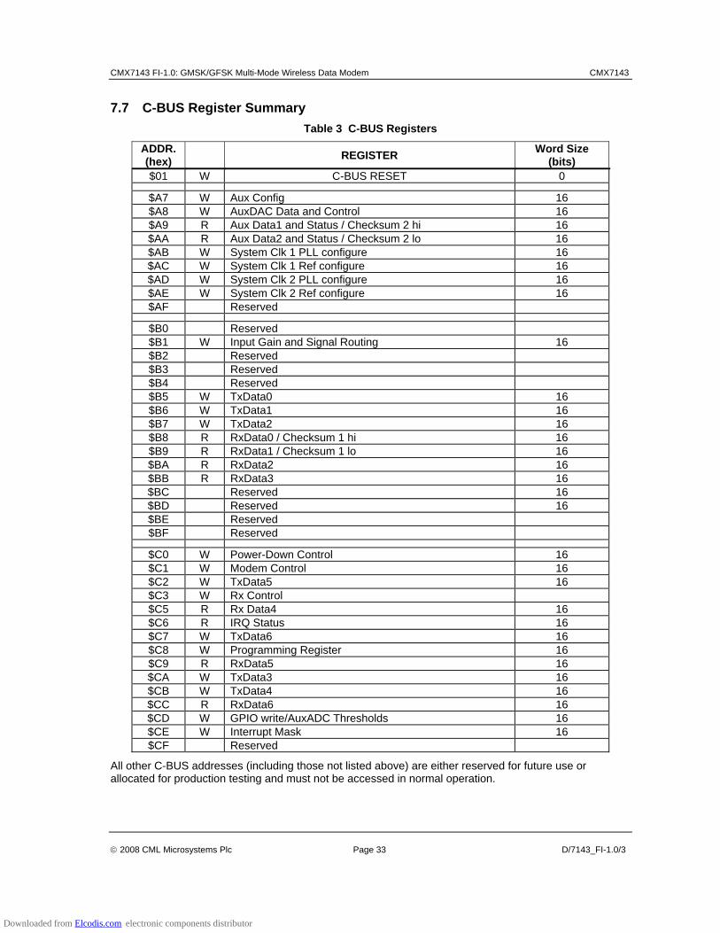
CMX7143 FI-1.0: GMSK/GFSK Multi-Mode Wireless Data Modem CMX7143
© 2008 CML Microsystems Plc Page 33 D/7143_FI-1.0/3
7.7 C-BUS Register Summary Table 3 C-BUS Registers
ADDR. (hex) REGISTER Word Size
(bits) $01 W C-BUS RESET 0
$A7 W Aux Config 16 $A8 W AuxDAC Data and Control 16 $A9 R Aux Data1 and Status / Checksum 2 hi 16 $AA R Aux Data2 and Status / Checksum 2 lo 16 $AB W System Clk 1 PLL configure 16 $AC W System Clk 1 Ref configure 16 $AD W System Clk 2 PLL configure 16 $AE W System Clk 2 Ref configure 16 $AF Reserved
$B0 Reserved $B1 W Input Gain and Signal Routing 16 $B2 Reserved $B3 Reserved $B4 Reserved $B5 W TxData0 16 $B6 W TxData1 16 $B7 W TxData2 16 $B8 R RxData0 / Checksum 1 hi 16 $B9 R RxData1 / Checksum 1 lo 16 $BA R RxData2 16 $BB R RxData3 16 $BC Reserved 16 $BD Reserved 16 $BE Reserved $BF Reserved
$C0 W Power-Down Control 16 $C1 W Modem Control 16 $C2 W TxData5 16 $C3 W Rx Control $C5 R Rx Data4 16 $C6 R IRQ Status 16 $C7 W TxData6 16 $C8 W Programming Register 16 $C9 R RxData5 16 $CA W TxData3 16 $CB W TxData4 16 $CC R RxData6 16 $CD W GPIO write/AuxADC Thresholds 16 $CE W Interrupt Mask 16 $CF Reserved
All other C-BUS addresses (including those not listed above) are either reserved for future use or allocated for production testing and must not be accessed in normal operation.
Downloaded from Elcodis.com electronic components distributor
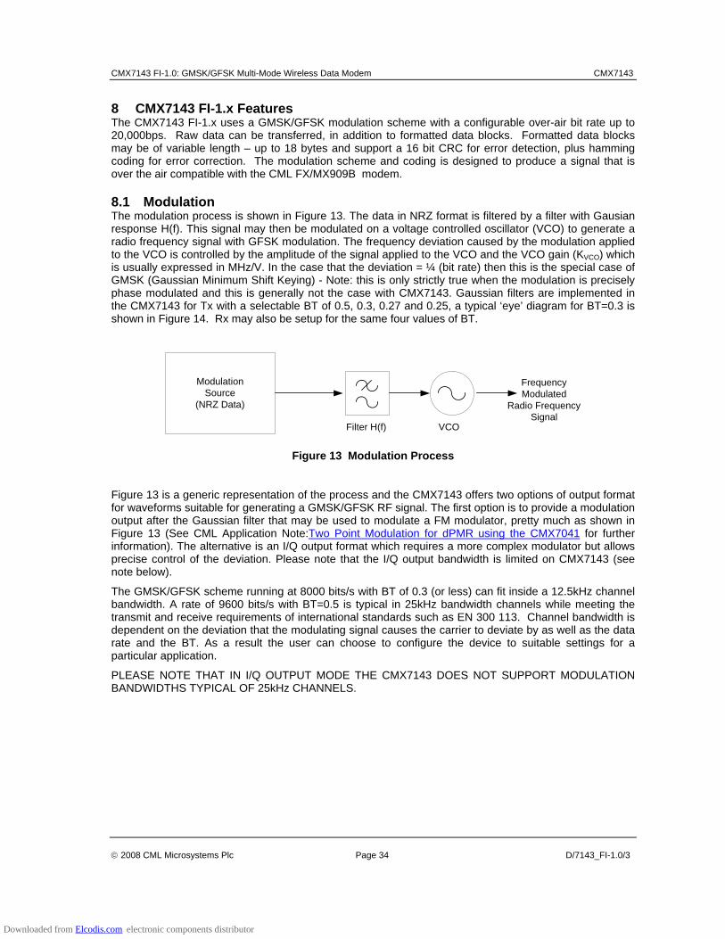
CMX7143 FI-1.0: GMSK/GFSK Multi-Mode Wireless Data Modem CMX7143
© 2008 CML Microsystems Plc Page 34 D/7143_FI-1.0/3
8 CMX7143 FI-1.x Features The CMX7143 FI-1.x uses a GMSK/GFSK modulation scheme with a configurable over-air bit rate up to 20,000bps. Raw data can be transferred, in addition to formatted data blocks. Formatted data blocks may be of variable length – up to 18 bytes and support a 16 bit CRC for error detection, plus hamming coding for error correction. The modulation scheme and coding is designed to produce a signal that is over the air compatible with the CML FX/MX909B modem.
8.1 Modulation The modulation process is shown in Figure 13. The data in NRZ format is filtered by a filter with Gausian response H(f). This signal may then be modulated on a voltage controlled oscillator (VCO) to generate a radio frequency signal with GFSK modulation. The frequency deviation caused by the modulation applied to the VCO is controlled by the amplitude of the signal applied to the VCO and the VCO gain (KVCO) which is usually expressed in MHz/V. In the case that the deviation = ¼ (bit rate) then this is the special case of GMSK (Gaussian Minimum Shift Keying) - Note: this is only strictly true when the modulation is precisely phase modulated and this is generally not the case with CMX7143. Gaussian filters are implemented in the CMX7143 for Tx with a selectable BT of 0.5, 0.3, 0.27 and 0.25, a typical ‘eye’ diagram for BT=0.3 is shown in Figure 14. Rx may also be setup for the same four values of BT.
FrequencyModulated
Radio FrequencySignal
VCOModulation
Source(NRZ Data)
VCOFilter H(f)
Figure 13 Modulation Process
Figure 13 is a generic representation of the process and the CMX7143 offers two options of output format for waveforms suitable for generating a GMSK/GFSK RF signal. The first option is to provide a modulation output after the Gaussian filter that may be used to modulate a FM modulator, pretty much as shown in Figure 13 (See CML Application Note:Two Point Modulation for dPMR using the CMX7041 for further information). The alternative is an I/Q output format which requires a more complex modulator but allows precise control of the deviation. Please note that the I/Q output bandwidth is limited on CMX7143 (see note below).
The GMSK/GFSK scheme running at 8000 bits/s with BT of 0.3 (or less) can fit inside a 12.5kHz channel bandwidth. A rate of 9600 bits/s with BT=0.5 is typical in 25kHz bandwidth channels while meeting the transmit and receive requirements of international standards such as EN 300 113. Channel bandwidth is dependent on the deviation that the modulating signal causes the carrier to deviate by as well as the data rate and the BT. As a result the user can choose to configure the device to suitable settings for a particular application.
PLEASE NOTE THAT IN I/Q OUTPUT MODE THE CMX7143 DOES NOT SUPPORT MODULATION BANDWIDTHS TYPICAL OF 25kHz CHANNELS.
Downloaded from Elcodis.com electronic components distributor
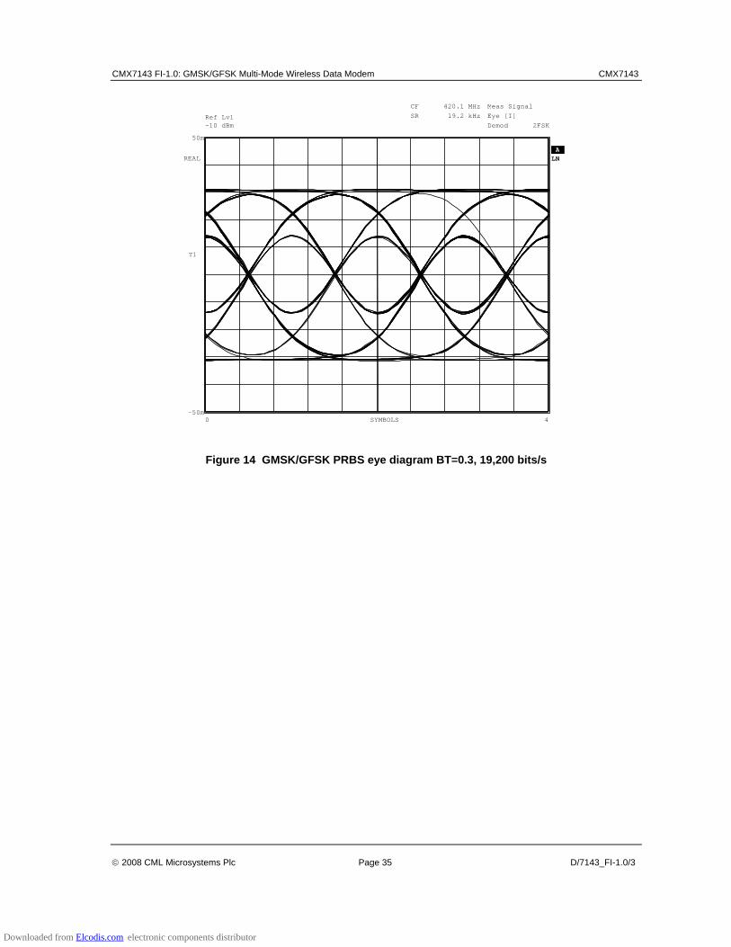
CMX7143 FI-1.0: GMSK/GFSK Multi-Mode Wireless Data Modem CMX7143
© 2008 CML Microsystems Plc Page 35 D/7143_FI-1.0/3
R e f L vl- 1 0 d Bm- 1 0 d BmR e f L vl- 1 0 d Bm- 1 0 d Bm
A L N L N
CF 420.1 MHzSR 19.2 kHz
Meas S i g n a l Eye [ I ] Demod 2 F S K
R E A L
T 1
0 4 SYMBOLS- 5 0 m
5 0 m
Figure 14 GMSK/GFSK PRBS eye diagram BT=0.3, 19,200 bits/s
Downloaded from Elcodis.com electronic components distributor

CMX7143 FI-1.0: GMSK/GFSK Multi-Mode Wireless Data Modem CMX7143
© 2008 CML Microsystems Plc Page 36 D/7143_FI-1.0/3
8.2 Radio Interface The CMX7143 is designed to process a demodulated signal from a limiter / discriminator source. For optimum performance, it is important that the demodulated signal is not significantly degraded by narrow filters and / or group delay distortion. NOTE: I,Q format is not supported in receive mode.
In transmit the CMX7143 can be configured to output a 2 point modulation signal, or a modulated I,Q output signal with programmable deviation (NOTE: See section 8.1).
An overview of how the CMX7143 might integrate with a limiter discriminator receiver, and 2 point modulation transmitter is shown in Figure 15.
2 x ADC
CMX7143
HOSTuP
2 x DAC
Power Amplifier
Reference (e.g VCTCXO)
VCO
PLL
T/R
RSSI
MOD1MOD2
Data (RxSig)
RSSI
Local Oscillator Local Oscillator
ControlVoltageInput
RAMDAC (Aux DAC1)
PA Gain Control
Figure 15 Outline Radio Design
Downloaded from Elcodis.com electronic components distributor

CMX7143 FI-1.0: GMSK/GFSK Multi-Mode Wireless Data Modem CMX7143
© 2008 CML Microsystems Plc Page 37 D/7143_FI-1.0/3
8.3 Formatted Data The CMX7143 1.x supports formatted data, which provides the ability to channel code blocks of data using hamming coding and CRCs. The Frame Structure as used in a formatted data system is illustrated in Figure 16 Formatted Data Over Air Signal Format, it typically consists of a Frame Head followed by several data blocks. A framesync with no control bytes may be substituted for the frame head.
Figure 16 Formatted Data Over Air Signal Format
The 'Frame head' may be used to contain addressing and control flag information. The 'Data' block(s) contain user data, and an optional checksum. The CMX7143 performs all of the block formatting and de-formatting, the binary data transferred between the modem and its µC being that enclosed by the thick dashed rectangles near the top of Figure 16 Formatted Data Over Air Signal Format. When receiving CRC protected blocks the CMX7143 will indicate CRC success or failure and will provide the data regardless.
Downloaded from Elcodis.com electronic components distributor
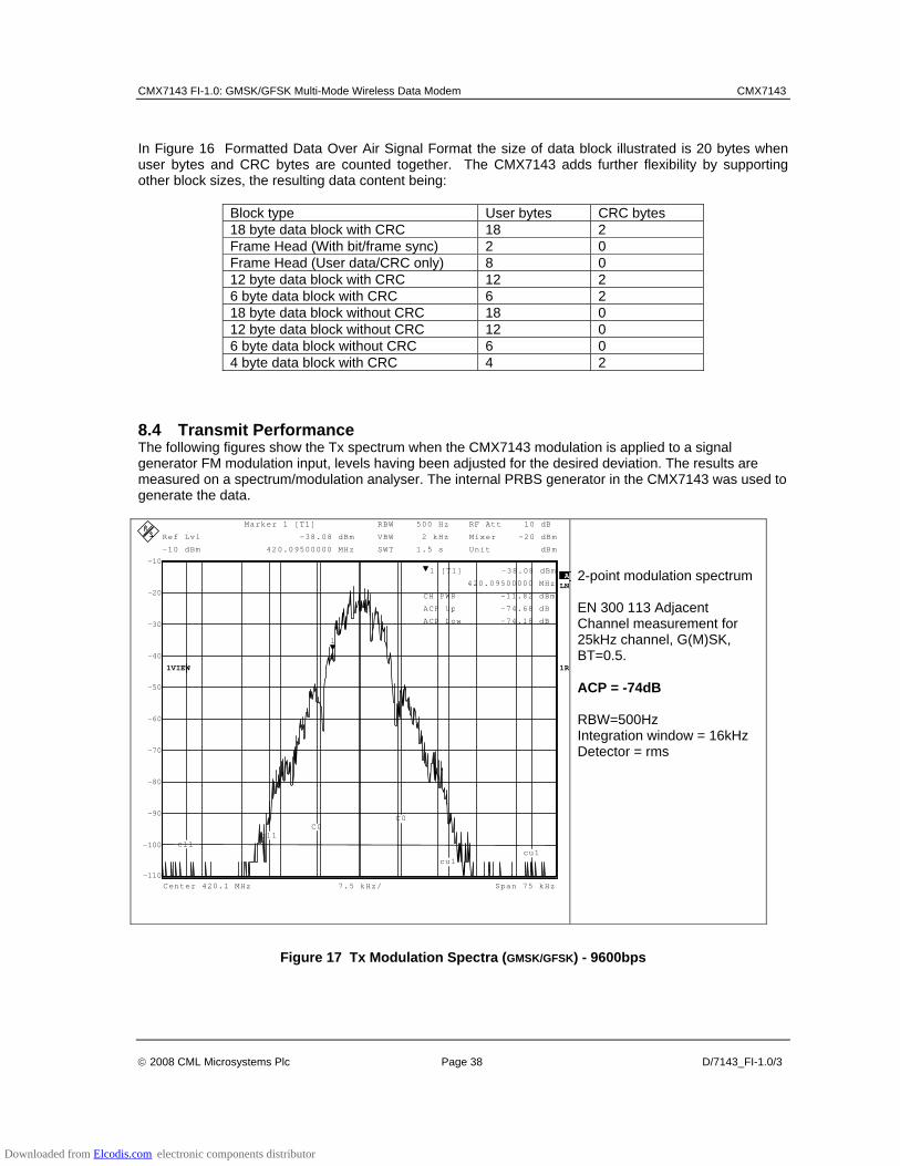
CMX7143 FI-1.0: GMSK/GFSK Multi-Mode Wireless Data Modem CMX7143
© 2008 CML Microsystems Plc Page 38 D/7143_FI-1.0/3
In Figure 16 Formatted Data Over Air Signal Format the size of data block illustrated is 20 bytes when user bytes and CRC bytes are counted together. The CMX7143 adds further flexibility by supporting other block sizes, the resulting data content being:
Block type User bytes CRC bytes 18 byte data block with CRC 18 2 Frame Head (With bit/frame sync) 2 0 Frame Head (User data/CRC only) 8 0 12 byte data block with CRC 12 2 6 byte data block with CRC 6 2 18 byte data block without CRC 18 0 12 byte data block without CRC 12 0 6 byte data block without CRC 6 0 4 byte data block with CRC 4 2
8.4 Transmit Performance The following figures show the Tx spectrum when the CMX7143 modulation is applied to a signal generator FM modulation input, levels having been adjusted for the desired deviation. The results are measured on a spectrum/modulation analyser. The internal PRBS generator in the CMX7143 was used to generate the data.
ALNLN
Unit dBm
Mixer -20 dBmR e f L v l - 1 0 d B m R e f L v l - 1 0 d B m
RF Att 10 dB
C e n t e r 4 2 0 . 1 M H z Span 75 kHz7 . 5 k H z /
RBW 500 Hz
SWT 1.5 s
VBW 2 kHz
1 V I E W 1RM
- 1 0 0
- 9 0
- 8 0
- 7 0
- 6 0
- 5 0
- 4 0
- 3 0
- 2 0
- 1 1 0
- 1 0
1
M a r k e r 1 [ T 1 ] - 3 8 . 0 8 d B m
4 2 0.09 5 0 0 0 0 0 M H z 1 [T1] -38.08 dBm
420.09500000 MHz
CH PWR -11.82 dBm
ACP Up -74.68 dB
ACP Low -74.18 dB
cu1cu1
c l 1 c l 1 C 0 C0
2-point modulation spectrum EN 300 113 Adjacent Channel measurement for 25kHz channel, G(M)SK, BT=0.5. ACP = -74dB RBW=500Hz Integration window = 16kHz Detector = rms
Figure 17 Tx Modulation Spectra (GMSK/GFSK) - 9600bps
Downloaded from Elcodis.com electronic components distributor
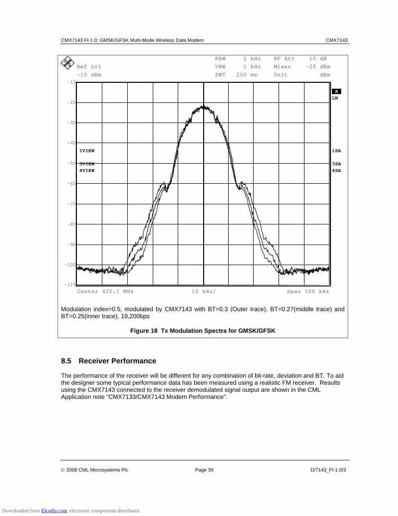
CMX7143 FI-1.0: GMSK/GFSK Multi-Mode Wireless Data Modem CMX7143
© 2008 CML Microsystems Plc Page 39 D/7143_FI-1.0/3
R e f L v l - 1 0 d B m R e f L v l - 1 0 d B m
A LNLN
C e n t e r 4 2 0 . 1 MH z S p a n 1 0 0 kHz
RBW 1 kHzVBW 1 kHzSWT 250 ms
M i x e r - 2 0 dBmU n i t dBm
10 kHz/
R F A t t 1 0 dB
1SA
3SA4SA
1 V I E W
3 V I E W 4 V I E W 4 V I E W 4SA
- 1 0 0
- 9 0
- 8 0
- 7 0
- 6 0
- 5 0
- 4 0
- 3 0
- 2 0
- 1 1 0
- 1 0
Modulation index=0.5, modulated by CMX7143 with BT=0.3 (Outer trace), BT=0.27(middle trace) and BT=0.25(inner trace), 19,200bps
Figure 18 Tx Modulation Spectra for GMSK/GFSK
8.5 Receiver Performance The performance of the receiver will be different for any combination of bit-rate, deviation and BT. To aid the designer some typical performance data has been measured using a realistic FM receiver. Results using the CMX7143 connected to the receiver demodulated signal output are shown in the CML Application note “CMX7133/CMX7143 Modem Performance”.
Downloaded from Elcodis.com electronic components distributor
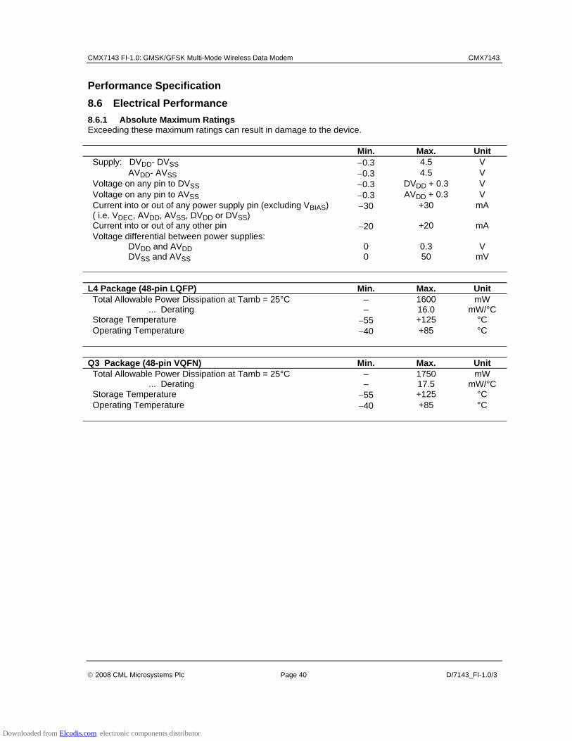
CMX7143 FI-1.0: GMSK/GFSK Multi-Mode Wireless Data Modem CMX7143
© 2008 CML Microsystems Plc Page 40 D/7143_FI-1.0/3
Performance Specification 8.6 Electrical Performance 8.6.1 Absolute Maximum Ratings Exceeding these maximum ratings can result in damage to the device. Min. Max. Unit Supply: DVDD- DVSS −0.3 4.5 V
AVDD- AVSS −0.3 4.5 V Voltage on any pin to DVSS −0.3 DVDD + 0.3 V Voltage on any pin to AVSS −0.3 AVDD + 0.3 V Current into or out of any power supply pin (excluding VBIAS) ( i.e. VDEC, AVDD, AVSS, DVDD or DVSS)
−30 +30 mA
Current into or out of any other pin −20 +20 mA Voltage differential between power supplies:
DVDD and AVDD 0 0.3 V DVSS and AVSS 0 50 mV
L4 Package (48-pin LQFP) Min. Max. Unit Total Allowable Power Dissipation at Tamb = 25°C – 1600 mW
... Derating – 16.0 mW/°C Storage Temperature −55 +125 °C Operating Temperature −40 +85 °C Q3 Package (48-pin VQFN) Min. Max. Unit Total Allowable Power Dissipation at Tamb = 25°C – 1750 mW
... Derating – 17.5 mW/°C Storage Temperature −55 +125 °C Operating Temperature −40 +85 °C
Downloaded from Elcodis.com electronic components distributor
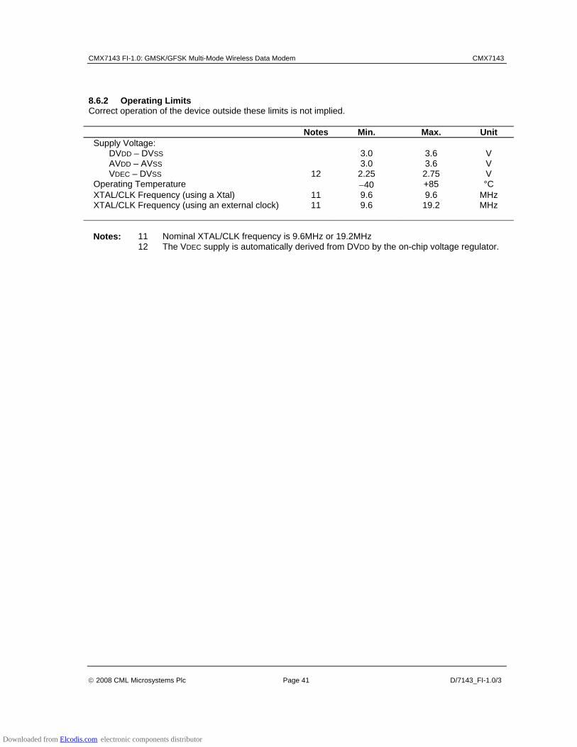
CMX7143 FI-1.0: GMSK/GFSK Multi-Mode Wireless Data Modem CMX7143
© 2008 CML Microsystems Plc Page 41 D/7143_FI-1.0/3
8.6.2 Operating Limits Correct operation of the device outside these limits is not implied. Notes Min. Max. Unit Supply Voltage: DVDD – DVSS 3.0 3.6 V AVDD – AVSS 3.0 3.6 V VDEC – DVSS 12 2.25 2.75 V Operating Temperature −40 +85 °C XTAL/CLK Frequency (using a Xtal) 11 9.6 9.6 MHz XTAL/CLK Frequency (using an external clock) 11 9.6 19.2 MHz Notes: 11 Nominal XTAL/CLK frequency is 9.6MHz or 19.2MHz 12 The VDEC supply is automatically derived from DVDD by the on-chip voltage regulator.
Downloaded from Elcodis.com electronic components distributor
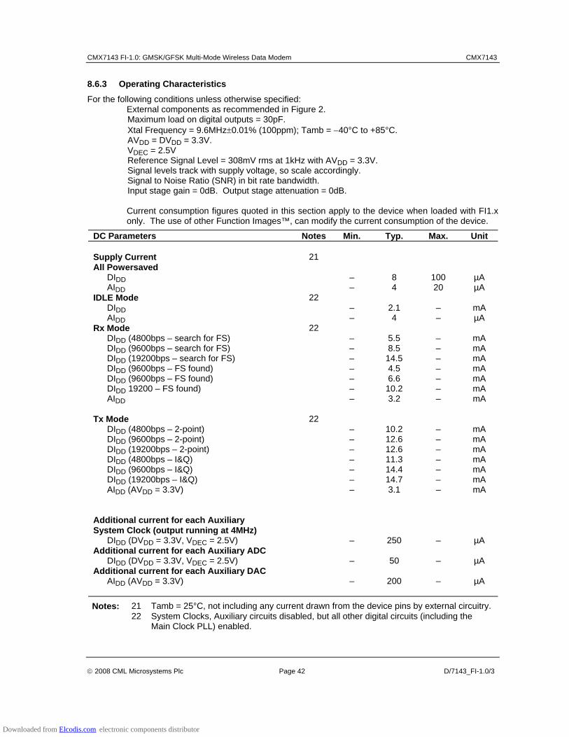
CMX7143 FI-1.0: GMSK/GFSK Multi-Mode Wireless Data Modem CMX7143
© 2008 CML Microsystems Plc Page 42 D/7143_FI-1.0/3
8.6.3 Operating Characteristics
For the following conditions unless otherwise specified: External components as recommended in Figure 2. Maximum load on digital outputs = 30pF. Xtal Frequency = 9.6MHz±0.01% (100ppm); Tamb = −40°C to +85°C. AVDD = DVDD = 3.3V. VDEC = 2.5V Reference Signal Level = 308mV rms at 1kHz with AVDD = 3.3V. Signal levels track with supply voltage, so scale accordingly. Signal to Noise Ratio (SNR) in bit rate bandwidth. Input stage gain = 0dB. Output stage attenuation = 0dB. Current consumption figures quoted in this section apply to the device when loaded with FI1.x only. The use of other Function Images™, can modify the current consumption of the device.
DC Parameters Notes Min. Typ. Max. Unit Supply Current 21 All Powersaved DIDD – 8 100 µA AIDD – 4 20 µA IDLE Mode 22 DIDD – 2.1 – mA AIDD – 4 – µA Rx Mode 22 DIDD (4800bps – search for FS) – 5.5 – mA DIDD (9600bps – search for FS) – 8.5 – mA DIDD (19200bps – search for FS) – 14.5 – mA DIDD (9600bps – FS found) – 4.5 – mA DIDD (9600bps – FS found) – 6.6 – mA DIDD 19200 – FS found) – 10.2 – mA AIDD – 3.2 – mA Tx Mode 22 DIDD (4800bps – 2-point) – 10.2 – mA DIDD (9600bps – 2-point) – 12.6 – mA DIDD (19200bps – 2-point) – 12.6 – mA DIDD (4800bps – I&Q) – 11.3 – mA DIDD (9600bps – I&Q) – 14.4 – mA DIDD (19200bps – I&Q) – 14.7 – mA AIDD (AVDD = 3.3V) – 3.1 – mA Additional current for each Auxiliary System Clock (output running at 4MHz)
DIDD (DVDD = 3.3V, VDEC = 2.5V) – 250 – µA Additional current for each Auxiliary ADC DIDD (DVDD = 3.3V, VDEC = 2.5V) – 50 – µA Additional current for each Auxiliary DAC AIDD (AVDD = 3.3V) – 200 – µA
Notes: 21 Tamb = 25°C, not including any current drawn from the device pins by external circuitry. 22 System Clocks, Auxiliary circuits disabled, but all other digital circuits (including the
Main Clock PLL) enabled.
Downloaded from Elcodis.com electronic components distributor
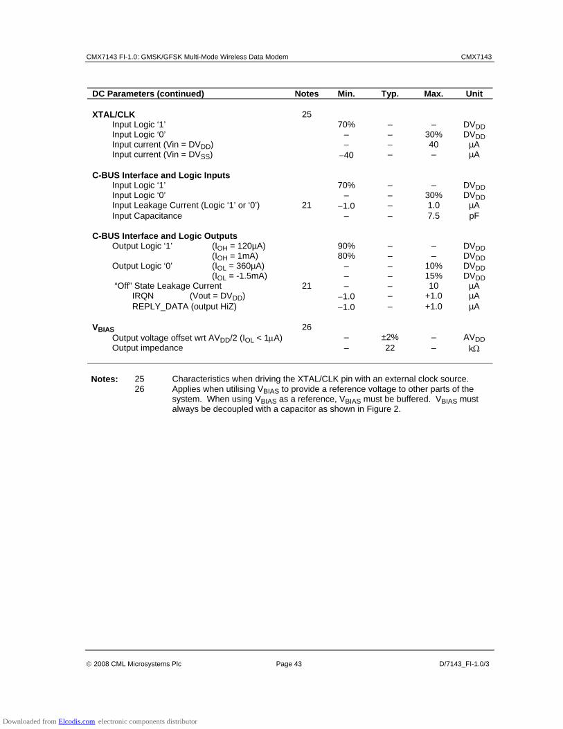
CMX7143 FI-1.0: GMSK/GFSK Multi-Mode Wireless Data Modem CMX7143
© 2008 CML Microsystems Plc Page 43 D/7143_FI-1.0/3
DC Parameters (continued) Notes Min. Typ. Max. Unit XTAL/CLK 25
Input Logic ‘1’ 70% – – DVDD Input Logic ‘0’ – – 30% DVDD Input current (Vin = DVDD) – – 40 µA Input current (Vin = DVSS) −40 – – µA
C-BUS Interface and Logic Inputs
Input Logic ‘1’ 70% – – DVDD Input Logic ‘0’ – – 30% DVDD Input Leakage Current (Logic ‘1’ or ‘0’) 21 −1.0 – 1.0 µA Input Capacitance – – 7.5 pF
C-BUS Interface and Logic Outputs
Output Logic ‘1’ (IOH = 120µA) 90% – – DVDD (IOH = 1mA) 80% – – DVDD Output Logic ‘0’ (IOL = 360µA) – – 10% DVDD (IOL = -1.5mA) – – 15% DVDD “Off” State Leakage Current 21 – – 10 µA
IRQN (Vout = DVDD) −1.0 – +1.0 µA REPLY_DATA (output HiZ) −1.0 – +1.0 µA
VBIAS 26
Output voltage offset wrt AVDD/2 (IOL < 1μA) – ±2% – AVDD Output impedance – 22 – kΩ
Notes: 25 Characteristics when driving the XTAL/CLK pin with an external clock source. 26 Applies when utilising VBIAS to provide a reference voltage to other parts of the
system. When using VBIAS as a reference, VBIAS must be buffered. VBIAS must always be decoupled with a capacitor as shown in Figure 2.
Downloaded from Elcodis.com electronic components distributor

CMX7143 FI-1.0: GMSK/GFSK Multi-Mode Wireless Data Modem CMX7143
© 2008 CML Microsystems Plc Page 44 D/7143_FI-1.0/3
AC Parameters Notes Min. Typ. Max. Unit XTAL/CLK Input
'High' pulse width 31 15 – – ns 'Low' pulse width 31 15 – – ns Input impedance (at 9.6MHz)
Powered-up Resistance – 150 – kΩ Capacitance – 20 – pF Powered-down Resistance – 300 – kΩ Capacitance – 20 – pF
Xtal start up (from powersave) – 20 – ms Auxiliary System Clk 1/2 Outputs
XTAL/CLK input to CLOCK_OUT timing: (in high to out high) 32 – 15 – ns (in low to out low) 32 – 15 – ns 'High' pulse width 33 48 52.08 56 ns 'Low' pulse width 33 48 52.08 56 ns
VBIAS Start up time (from powersave) – 30 – ms
CH1,2 and 3 inputs (RxSig/RSSI 1,2 and 3) Input impedance 34 – 1 – MΩ Maximum Input Level (pk-pk) 35 – – 80% AVDD Load resistance (feedback pins) 80 – – kΩ Amplifier open loop voltage gain ⎫
(I/P = 1mV rms at 100Hz) ⎭ – 80 – dB Unity gain bandwidth – 1.0 – MHz Programmable Input Gain Stage 36 Gain (at 0dB) 37 −0.5 0 +0.5 dB Cumulative Gain Error ⎫
(wrt attenuation at 0dB) ⎭ 37 −1.0 0 +1.0 dB
Notes: 31 Timing for an external input to the XTAL/CLK pin. 32 XTAL/CLK input driven by an external source. 33 9.6MHz XTAL fitted and 9.6MHz output selected. 34 With no external components connected 35 Centered about AVDD/2; after multiplying by the gain of input circuit (with external
components connected). 36 Gain applied to signal at output of buffer amplifier: CH1FB, CH2FB or CH3FB. 37 Design Value. Overall attenuation input to output has a tolerance of 0dB ±1.0dB
Downloaded from Elcodis.com electronic components distributor

CMX7143 FI-1.0: GMSK/GFSK Multi-Mode Wireless Data Modem CMX7143
© 2008 CML Microsystems Plc Page 45 D/7143_FI-1.0/3
AC Parameters Notes Min. Typ. Max. Unit Modulator Outputs 1/2 (MOD 1, MOD 2)
Power-up to output stable 41 – 50 100 µs Modulator Attenuators Attenuation (at 0dB) 43 −1.0 0 +1.0 dB Cumulative Attenuation Error ⎫
(wrt attenuation at 0dB) ⎭ −0.6 0 +0.6 dB Output Impedance ⎫ Enabled 42 – 600 – Ω ⎭ Disabled 42 – 500 – kΩ Output current range (AVDD = 3.3V) – – ±125 µA Output voltage range 44 0.5 – AVDD –0.5 V Load resistance 20 – – kΩ
Notes: 41 Power-up refers to issuing a C-BUS command to turn on an output. These limits
apply only if VBIAS is on and stable. At power supply switch-on, the default state is for all blocks, except the XTAL and C-BUS interface, to be in placed in powersave mode.
42 Small signal impedance, at AVDD = 3.3V and Tamb = 25°C. 43 With respect to the signal at the feedback pin of the selected input port. 44 Centered about AVDD/2; with respect to the output driving a 20kΩ load to AVDD/2.
Downloaded from Elcodis.com electronic components distributor

CMX7143 FI-1.0: GMSK/GFSK Multi-Mode Wireless Data Modem CMX7143
© 2008 CML Microsystems Plc Page 46 D/7143_FI-1.0/3
AC Parameters (cont.) Notes Min. Typ. Max. Unit Auxiliary Signal Inputs (Aux ADC 1 to 4)
Source Output Impedance 51 – – 24 kΩ
Auxiliary 10 Bit ADCs Resolution – 10 – Bits Maximum Input Level (pk-pk) 54 – – 80% AVDD Input impedance
Resistance – 10 – MΩ Capacitance – 5 – pF
Zero error ⎫ (input offset to give ADC output = 0) ⎭ 0 – ±10 mV
Integral Non-linearity – – ±3 LSBs Differential Non-linearity 53 – – ±1 LSBs
Auxiliary 10 Bit DACs Resolution – 10 – Bits Maximum Output Level (pk-pk), no load 54 80% – – AVDD Zero error ⎫
(output offset from a DAC input = 0) ⎭ 0 – ±10 mV Resistive Load 5 – – kΩ Integral Non-linearity – – ±4 LSBs Differential Non-linearity 53 – – ±1 LSBs
Notes: 51 Denotes output impedance of the driver of the auxiliary input signal, to ensure
< 1 bit additional error under nominal conditions. 53 Guaranteed monotonic with no missing codes. 54 Centred about AVDD/2.
Downloaded from Elcodis.com electronic components distributor
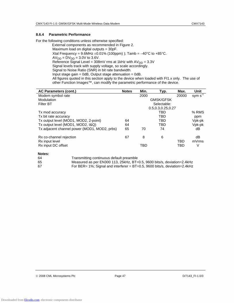
CMX7143 FI-1.0: GMSK/GFSK Multi-Mode Wireless Data Modem CMX7143
© 2008 CML Microsystems Plc Page 47 D/7143_FI-1.0/3
8.6.4 Parametric Performance
For the following conditions unless otherwise specified: External components as recommended in Figure 2. Maximum load on digital outputs = 30pF. Xtal Frequency = 9.6MHz ±0.01% (100ppm) ); Tamb = −40°C to +85°C. AVDD = DVDD = 3.0V to 3.6V. Reference Signal Level = 308mV rms at 1kHz with AVDD = 3.3V Signal levels track with supply voltage, so scale accordingly. Signal to Noise Ratio (SNR) in bit rate bandwidth. Input stage gain = 0dB, Output stage attenuation = 0dB. All figures quoted in this section apply to the device when loaded with FI1.x only. The use of other Function Images™, can modify the parametric performance of the device.
AC Parameters (cont.) Notes Min. Typ. Max. Unit Modem symbol rate 2000 20000 sym s-1 Modulation GMSK/GFSK Filter BT Selectable:
0.5,0.3,0.25,0.27
Tx mod accuracy TBD % RMSTx bit rate accuracy TBD ppm Tx output level (MOD1, MOD2, 2-point) 64 TBD Vpk-pk Tx output level (MOD1, MOD2, I&Q) 64 TBD Vpk-pk Tx adjacent channel power (MOD1, MOD2, prbs) 65 70 74 dB Rx co-channel rejection 67 8 6 dB Rx input level TBD mVrms Rx input DC offset TBD TBD V
Notes: 64 Transmitting continuous default preamble 65 Measured as per EN300 113, 25kHz, BT=0.5, 9600 bits/s, deviation=2.4kHz 67 For BER= 1%; Signal and interferer = BT=0.5, 9600 bits/s, deviation=2.4kHz
Downloaded from Elcodis.com electronic components distributor

CMX7143 FI-1.0: GMSK/GFSK Multi-Mode Wireless Data Modem CMX7143
© 2008 CML Microsystems Plc Page 48 D/7143_FI-1.0/3
C-BUS Timing
Figure 19 C-BUS Timing
C-BUS Timing Notes Min. Typ. Max. Unit tCSE CSN Enable to SClk high time 100 – – ns tCSH Last SClk high to CSN high time 100 – – ns tLOZ SClk low to ReplyData Output Enable
Time 0.0 – – ns
tHIZ CSN high to ReplyData high impedance – – 1.0 µs tCSOFF CSN high time between transactions 1.0 – – µs tNXT Inter-byte time 200 – – ns tCK SClk cycle time 200 – – ns tCH SClk high time 100 – – ns tCL SClk low time 100 – – ns tCDS Command Data setup time 75 – – ns tCDH Command Data hold time 25 – – ns tRDS Reply Data setup time 50 – – ns tRDH Reply Data hold time 0 – – ns Notes: 1. Depending on the command, 1 or 2 bytes of COMMAND DATA are transmitted to the
peripheral MSB (Bit 7) first, LSB (Bit 0) last. REPLY DATA is read from the peripheral MSB (Bit 7) first, LSB (Bit 0) last.
2. Data is clocked into the peripheral on the rising SERIAL_CLOCK edge. 3. Commands are acted upon at the end of each command (rising edge of CSN). 4. To allow for differing µC serial interface formats C-BUS compatible ICs are able to work
with SERIAL_CLOCK pulses starting and ending at either polarity. 5. Maximum 30pF load on IRQN pin and each C-BUS interface line. These timings are for the latest version of C-BUS and allow faster transfers than the original C-BUS timing specification. The CMX7143 can be used in conjunction with devices that comply with the slower timings, subject to system throughput constraints.
Downloaded from Elcodis.com electronic components distributor
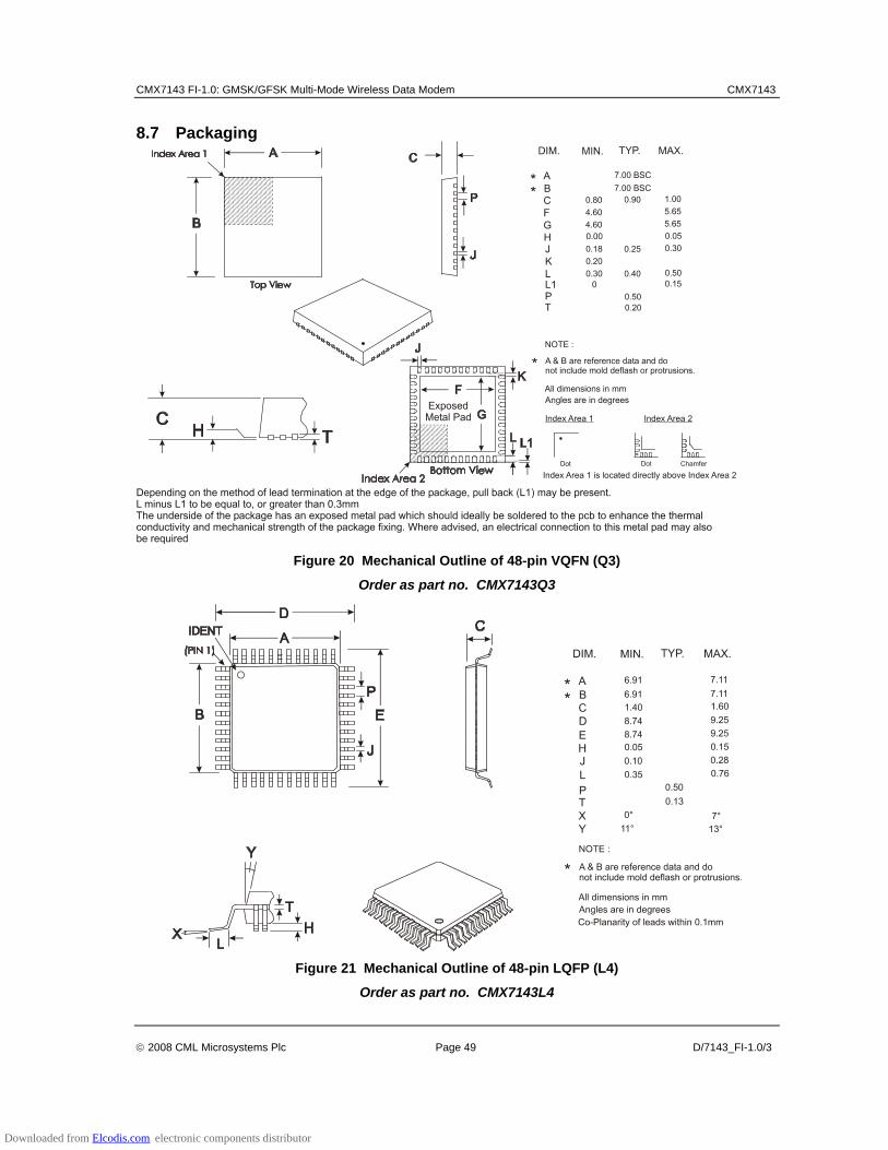
CMX7143 FI-1.0: GMSK/GFSK Multi-Mode Wireless Data Modem CMX7143
© 2008 CML Microsystems Plc Page 49 D/7143_FI-1.0/3
8.7 Packaging
Figure 20 Mechanical Outline of 48-pin VQFN (Q3)
Order as part no. CMX7143Q3
Figure 21 Mechanical Outline of 48-pin LQFP (L4)
Order as part no. CMX7143L4
Downloaded from Elcodis.com electronic components distributor

CMX7143 FI-1.0: GMSK/GFSK Multi-Mode Wireless Data Modem CMX7143
© 2008 CML Microsystems Plc Page 50 D/7143_FI-1.0/3
As package dimensions may change after publication of this datasheet, it is recommended that you check for the latest Packaging Information from the Datasheets page of the CML website: [www.cmlmicro.com].
About FirmASIC®
CML’s proprietary FirmASIC® component technology reduces cost, time to market and development risk, with increased flexibility for the designer and end application. FirmASIC® combines Analogue, Digital, Firmware and Memory technologies in a single silicon platform that can be focused to deliver the right feature mix, performance and price for a target application family. Specific functions of a FirmASIC® device are determined by uploading its Function Image™ during device initialization. New Function Images™ may be later provided to supplement and enhance device functions, expanding or modifying end-product features without the need for expensive and time-consuming design changes. FirmASIC® devices provide significant time to market and commercial benefits over Custom ASIC, Structured ASIC, FPGA and DSP solutions. They may also be exclusively customised where security or intellectual property issues prevent the use of Application Specific Standard Products (ASSP’s).
Handling precautions: This product includes input protection, however, precautions should be taken to prevent device damage from electro-static discharge. CML does not assume any responsibility for the use of any circuitry described. No IPR or circuit patent licences are implied. CML reserves the right at any time without notice to change the said circuitry and this product specification. CML has a policy of testing every product shipped using calibrated test equipment to ensure compliance with this product specification. Specific testing of all circuit parameters is not necessarily performed.
Downloaded from Elcodis.com electronic components distributor

![Mobile, Wireless and Pervasive Computing [Compatibility Mode]](https://static.fdocuments.us/doc/165x107/58887e2a1a28aba76b8be877/mobile-wireless-and-pervasive-computing-compatibility-mode.jpg)