circuit analysis. My Homework. Karl S. Bogha.
233
Chapter 7 Part 3D. Op Amp, RLC, and Technique For Synthesizing H(s). Source of study material: 1). Electric Circuits 6th Ed Schaums - Nahvi & Edminister. 2). Engineering Circuits Analysis - Hyat & Kemmerly. 3). Operational Amplifiers and Linear Integrated Circuits 6th Ed- Coughlin & Driscoll. Pre-requisite study for Laplace Transforms in circuit analysis . My Homework . Karl S. Bogha. Part 3 D: RLC Higher Order Circuits Continuing Notes And Fully Solved Examples and Problems. 1). Section 1: Introduction To Operational Amplifiers (Op Amp) circuits. 2). Section 2: Continuation of Op Amp For Electric Circuits. 3). Section 3: Solving Problems On Op Amp Electric Circuits. 3). Section 4: Continuing From Part 3C. Approximately: 233 Pages. Level: Intermediate. Part 3D Section 4 bring an end to the purpose of the notes and problem solving which started from Part 1. Purpose: 1. Gain adequate understanding of electric circuits by completing specific pre-requisite topics before getting into Laplace Transforms In Circuit Analysis. 2. Working towards getting past the hurdle or obstacle topics in electric circuits so that student (UG/G) can progress successfully thru completion of Electric Circuits courses. These topics are related to R L C and OpAmps. 3. Thus continuing topics in electric circuits may pose a challenge but they should not be an obstacle in completing the course work for Circuits I and II. Typically Laplace Transforms do NOT appear till a signals/systems course in year 3, or controls course in year 3 or 4 of a 4 year program. Please note any interested technical party from any college in any country may use these notes for the same purpose. Apologies for any errors and omissions. 2nd March 2021. Engineering college year 2 course of 4 year program OR year 1 of 3 year program. Re-fresher OR Self Study. Graduate Study Review. May be used in New Zealand, US, Malaysia, India, Pakistan, UK, and other Common Wealth Country engineering colleges. Any errors and omissions apologies in advance.
Transcript of circuit analysis. My Homework. Karl S. Bogha.

Chapter 7 Part 3D. Op Amp, RLC, and Technique For Synthesizing H(s). Source of study material: 1). Electric Circuits 6th Ed Schaums - Nahvi & Edminister. 2). Engineering Circuits Analysis - Hyat & Kemmerly. 3). Operational Amplifiers and Linear Integrated Circuits 6th Ed- Coughlin & Driscoll. Pre-requisite study for Laplace Transforms in circuit analysis. My Homework. Karl S. Bogha.
Part 3 D:
RLC Higher Order Circuits Continuing Notes And Fully Solved Examples and Problems.
1). Section 1: Introduction To Operational Amplifiers (Op Amp) circuits.2). Section 2: Continuation of Op Amp For Electric Circuits.3). Section 3: Solving Problems On Op Amp Electric Circuits.3). Section 4: Continuing From Part 3C. Approximately: 233 Pages.Level: Intermediate.
Part 3D Section 4 bring an end to the purpose of the notes and problem solving which started from Part 1.
Purpose:
1. Gain adequate understanding of electric circuits by completing specific pre-requisite topics before getting into Laplace Transforms In Circuit Analysis.2. Working towards getting past the hurdle or obstacle topics in electric circuits so that student (UG/G) can progress successfully thru completion of Electric Circuits courses. These topics are related to R L C and OpAmps.3. Thus continuing topics in electric circuits may pose a challenge but they should not be an obstacle in completing the course work for Circuits I and II.
Typically Laplace Transforms do NOT appear till a signals/systems course inyear 3, or controls course in year 3 or 4 of a 4 year program. Please note any interested technical party from any college in any country may use these notes for the same purpose.
Apologies for any errors and omissions.2nd March 2021.
Engineering college year 2 course of 4 year program OR year 1 of 3 year program. Re-fresher OR Self Study. Graduate Study Review.May be used in New Zealand, US, Malaysia, India, Pakistan, UK, and other Common Wealth Country engineering colleges.Any errors and omissions apologies in advance.

Chapter 7 Part 3D. Op Amp, RLC, and Technique For Synthesizing H(s). Source of study material: 1). Electric Circuits 6th Ed Schaums - Nahvi & Edminister. 2). Engineering Circuits Analysis - Hyat & Kemmerly. 3). Operational Amplifiers and Linear Integrated Circuits 6th Ed- Coughlin & Driscoll. Pre-requisite study for Laplace Transforms in circuit analysis. My Homework. Karl S. Bogha.
Part 3 D:
RLC Higher Order Circuits Continuing Notes And Solved Examples and Problems.
Section 1: Introduction To Operational Amplifier (Op Amp) circuits.
I. Several parts of chapters 2, and 3 from Coughlin and Driscoll Op Amp Textbook. Providing notes and solved examples to build the knowledge before entering Schaums topics on Opamps. Often using the examples from Coughlin and Driscoll to assist elsewhere in Schaums Op Amp topics.
II. Schaums:
1. Amplifier model2. Feedback in amplifier circuits3. Operational amplifiers4. Analysis of circuits containing ideal Op Amps5. Inverting Op Amp6. Summing circuit7. Non-inverting circuits8. Voltage follower9. Differential and difference amplifiers10. Circuits containing several Op Amps
Followed by a sample Op Amp circuit called Servo Amplifier to build interest in Op Amps from Coughlin and Driscoll's textbook.
Section 2: Operational Amplifier (Op Amp) circuits.
I. Schaums:
11. Integrator and differentiator circuits12. Analog computers13. Low-pass filter14. Decibel (dB)15. Real Op Amp16. A simple Op Amp model 17. Comparator (Briefly)18. Flash analog to digital converter not on notes rather an example related to analog to digital converter was solved in Section 3.
Engineering college year 2 course of 4 year program OR year 1 of 3 year program. Re-fresher OR Self Study. Graduate Study Review.May be used in New Zealand, US, Malaysia, India, Pakistan, UK, and other Common Wealth Country engineering colleges.Any errors and omissions apologies in advance.

Chapter 7 Part 3D. Op Amp, RLC, and Technique For Synthesizing H(s). Source of study material: 1). Electric Circuits 6th Ed Schaums - Nahvi & Edminister. 2). Engineering Circuits Analysis - Hyat & Kemmerly. 3). Operational Amplifiers and Linear Integrated Circuits 6th Ed- Coughlin & Driscoll. Pre-requisite study for Laplace Transforms in circuit analysis. My Homework. Karl S. Bogha.
Section 3: Fully solving partially solved examples, partially solved problems, and supplementary problems.
Problems are related to Op Amp circuits.
Primarily the topics covered in Schaums.
Purpose is toget an understanding on how to approach solving Op Amp Active circuits. These are circuits with Op Amp and R L and C components.
There is a special topic covered from Chapter 7 of 4th edition of Hyat and Kemmerly the topic is on The Lossless LC Circuit from section 7-8. This topic is relevant to RLC studies.
Section 4:
1. Engineering Circuit Analysis Hyat and Kemmerly 4th Edition: Section 13-8: A Technique For Synthesizing The Voltage Ratio H(s) = Vout / Vin.
2. Schaums: Magnitude scaling
3. Schaums: Frequency scaling
4. Schaums: Higher order active circuits
Relevant 'partially solved examples, problems and supplementary problems' were solved. Electric Circuits textbooks have additional problems which can be worked on as required.
Apologies for any errors and omissions.2nd March 2021.
Engineering college year 2 course of 4 year program OR year 1 of 3 year program. Re-fresher OR Self Study. Graduate Study Review.May be used in New Zealand, US, Malaysia, India, Pakistan, UK, and other Common Wealth Country engineering colleges.Any errors and omissions apologies in advance.
Chapter 7 Part 3D. Op Amp, RLC, and Technique For Synthesizing H(s). Source of study material: 1). Electric Circuits 6th Ed Schaums - Nahvi & Edminister. 2). Engineering Circuits Analysis - Hyat & Kemmerly. 3). Operational Amplifiers and Linear Integrated Circuits 6th Ed- Coughlin & Driscoll. Pre-requisite study for Laplace Transforms in circuit analysis. My Homework. Karl S. Bogha.
Part 3 D: Section 1.
RLC Higher Order Circuits Continuing Notes And Solved Examples and Problems.
Section 1: Introduction To Operational Amplifier (Op Amp) circuits.
I. Several parts of chapters 2, and 3 from Coughlin and Driscoll Op Amp Textbook. Providing notes and solved examples to build the knowledge before entering Schaums topics on Opamps. Often using the examples from Coughlin and Driscoll to assist elsewhere in Schaums Op Amp topics.
II. Schaums:
1. Amplifier model2. Feedback in amplifier circuits3. Operational amplifiers4. Analysis of circuits containing ideal Op Amps5. Inverting Op Amp6. Summing circuit7. Non-inverting circuits8. Voltage follower9. Differential and difference amplifiers10. Circuits containing several Op Amps
Followed by a sample Op Amp circuit called Servo Amplifier to build interest in Op Amps from Coughlin and Driscoll's textbook.
Continuing to Section 2.
Apologies for any errors and omissions.
Engineering college year 2 course of 4 year program OR year 1 of 3 year program. Re-fresher OR Self Study. Graduate Study Review.May be used in New Zealand, US, Malaysia, India, Pakistan, UK, and other Common Wealth Country engineering colleges.Any errors and omissions apologies in advance.

Chapter 7 Part 3D. Op Amp, RLC, and Technique For Synthesizing H(s). Source of study material: 1). Electric Circuits 6th Ed Schaums - Nahvi & Edminister. 2). Engineering Circuits Analysis - Hyat & Kemmerly. 3). Operational Amplifiers and Linear Integrated Circuits 6th Ed- Coughlin & Driscoll. Pre-requisite study for Laplace Transforms in circuit analysis. My Homework. Karl S. Bogha.
Section 1
Operational Amplifier.
Its not a fancy name for the amplifier of a car stereo.It a small device that is used in the stereo amplifier and many other devices from critical devices to leisure devices.
It is a critical 'part or component' in electrical engineering.Whether you end up using it or designing circuits using it thats an employment matter, depends on what they do at the place you work.
What I want to do is use it as a component in electric circuits.The most common/starter Op Amp is the 741 its called the general purpose Op Amp.
I provide a few figures I re-sketched from the textbook Operational Amplifiers and Linear Integrated Circuits (6th Edition) by the engineers Coughlin and Driscoll (C&D).
1st figure: The block diagram of the internals of the Op Amp.
2nd figure: The electric circuit symbol layout of the device with terminal connection points.
3rd figure: A physical picture with the terminal numbers.
4th figure: The electric circuit Op Amp with brief description on the function and description of the main terminals connection.
Unlike R, L, and C components the Op Amp is an electronic device which used in electronic devices or products. Its not a single component, its made up of electronic components, and there are many types of op amps for many applications. Its an active device, not a passive (RLC) device. So some actual performance/application of the device needs to be worked too. Will give it a try here. The internals of the device, op amp, is powered by V+ and V-, which has to be supplied. The external circuit connections are made to terminals on the op amp. The input signal, dc or ac, is made to terminal 2 or 3 or both 2 and 3.
See next page.
Engineering college year 2 course of 4 year program OR year 1 of 3 year program. Re-fresher OR Self Study. Graduate Study Review.May be used in New Zealand, US, Malaysia, India, Pakistan, UK, and other Common Wealth Country engineering colleges.Any errors and omissions apologies in advance.

Chapter 7 Part 3D. Op Amp, RLC, and Technique For Synthesizing H(s). Source of study material: 1). Electric Circuits 6th Ed Schaums - Nahvi & Edminister. 2). Engineering Circuits Analysis - Hyat & Kemmerly. 3). Operational Amplifiers and Linear Integrated Circuits 6th Ed- Coughlin & Driscoll. Pre-requisite study for Laplace Transforms in circuit analysis. My Homework. Karl S. Bogha.
Figure 1: Op Amp internal circuitry block diagram (Not interested in this rather application).
Figure 2: Electric circuit symbol for Op Amp and connection points for the circuitry.
Engineering college year 2 course of 4 year program OR year 1 of 3 year program. Re-fresher OR Self Study. Graduate Study Review.May be used in New Zealand, US, Malaysia, India, Pakistan, UK, and other Common Wealth Country engineering colleges.Any errors and omissions apologies in advance.

Chapter 7 Part 3D. Op Amp, RLC, and Technique For Synthesizing H(s). Source of study material: 1). Electric Circuits 6th Ed Schaums - Nahvi & Edminister. 2). Engineering Circuits Analysis - Hyat & Kemmerly. 3). Operational Amplifiers and Linear Integrated Circuits 6th Ed- Coughlin & Driscoll. Pre-requisite study for Laplace Transforms in circuit analysis. My Homework. Karl S. Bogha.
There are several physical appearances of operational amplifiers ('opamps' / 'op amps').
Figure 3: 741 Op Amp physical layout and the terminal connections.
Picture to the right:Operational Amplifier textbook.Usually Op Amps are a chapter or more in the electronic textbook. Dedicated Op Amps textbook are not common. This textbook, shown to the left, has applications and theory on the Op Amps, several chapters with each looking at application and the core electronic studies related to Op Amps.
I recommend to you this book if youre serious about Op Amps to where you maybe want to make it your main device in your work or have need for many applicationsusing it. You maybe able to get a PDF copy on sale from the publisher, Pearson Prentice Hall, or used book copy.
There maybe recent books for your use .Check with your lecturer or local engineer.
Textbook name: Operational Amplifiers and Linear Integrated Circuits.6th Edition. Coughlin and Driscoll. 2001.
Pearson Prentice Hall.
Engineering college year 2 course of 4 year program OR year 1 of 3 year program. Re-fresher OR Self Study. Graduate Study Review.May be used in New Zealand, US, Malaysia, India, Pakistan, UK, and other Common Wealth Country engineering colleges.Any errors and omissions apologies in advance.

Chapter 7 Part 3D. Op Amp, RLC, and Technique For Synthesizing H(s). Source of study material: 1). Electric Circuits 6th Ed Schaums - Nahvi & Edminister. 2). Engineering Circuits Analysis - Hyat & Kemmerly. 3). Operational Amplifiers and Linear Integrated Circuits 6th Ed- Coughlin & Driscoll. Pre-requisite study for Laplace Transforms in circuit analysis. My Homework. Karl S. Bogha.
Figure 4: Brief description of 741 Op Amp's terminals.Hopefully for me I dont have to struggle so much on this since its been years when I first studied it. Since then maybe 2 billion Op Amps been manufactured? Maybe less half a billion, maybe 10 billion. I am not looking at the genius inside the Op-Amp, which successful engineers have created, just how to use it or what to expect from it in an electric circuit. It is a critical device like the other semiconductor devices.
Engineering college year 2 course of 4 year program OR year 1 of 3 year program. Re-fresher OR Self Study. Graduate Study Review.May be used in New Zealand, US, Malaysia, India, Pakistan, UK, and other Common Wealth Country engineering colleges.Any errors and omissions apologies in advance.
Chapter 7 Part 3D. Op Amp, RLC, and Technique For Synthesizing H(s). Source of study material: 1). Electric Circuits 6th Ed Schaums - Nahvi & Edminister. 2). Engineering Circuits Analysis - Hyat & Kemmerly. 3). Operational Amplifiers and Linear Integrated Circuits 6th Ed- Coughlin & Driscoll. Pre-requisite study for Laplace Transforms in circuit analysis. My Homework. Karl S. Bogha.
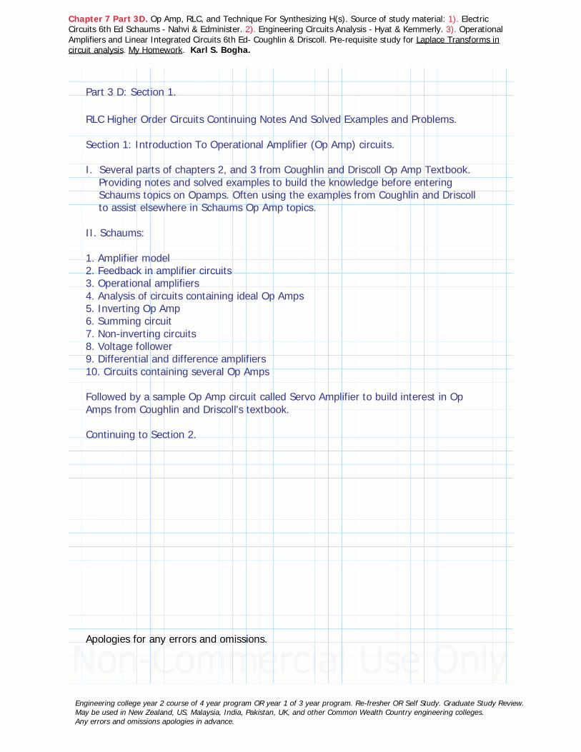
Figure above shows the following for an ideal 741 OpAmp:
Input resistance forRin_negative = ∞ Ohm
Rin_positive = ∞ Ohm
With resistance infinity, we assume current unable to pass thru hence it must be near zero amps. Except for a very negligible curent passing thru (-) or (+) terminal.
IB_negative = 0 A. Near zero.
IB_positive = 0 A. Near zero.
The output resistance for Ro = 0 Ohm
Gain A is given in the problem statement OR on the Op Amp specifications.Usually A OR A_OL.
So use these minimum conditions in the circuit analysis for starters.
I kick-off or kick-in with the information or notes on pages 45-47 of Driscoll.This is slightly jumping into the op amp situation but its mostly going over the few points given on the conditions on previous page. May be a little different to look at or compared to other circuits thus far I hope to get around it.
Engineering college year 2 course of 4 year program OR year 1 of 3 year program. Re-fresher OR Self Study. Graduate Study Review.May be used in New Zealand, US, Malaysia, India, Pakistan, UK, and other Common Wealth Country engineering colleges.Any errors and omissions apologies in advance.

Chapter 7 Part 3D. Op Amp, RLC, and Technique For Synthesizing H(s). Source of study material: 1). Electric Circuits 6th Ed Schaums - Nahvi & Edminister. 2). Engineering Circuits Analysis - Hyat & Kemmerly. 3). Operational Amplifiers and Linear Integrated Circuits 6th Ed- Coughlin & Driscoll. Pre-requisite study for Laplace Transforms in circuit analysis. My Homework. Karl S. Bogha.
Inverting Amplifier:
My first op amp circuit here, may assume some prior encounter with op amp, does not really start with an introduction or circuit example. But I will come to that later. Here I have some recollection and its workable thru the reference textbook. Get into it quicker.Ei:DC voltage Ei applied thru the -ve terminal 2, inverted terminal connection.Rf:Feedback, negative feedback is provided by the resistor Rf.
Voltage between terminal 3 (+) and 2 (-):Place one lead of a voltmeter on 2 and the other 3, reading will be zero volts. Terminal 3 is connected to earth. Terminal 2 does not see Ei connected to it, that is further from terminal 2 at the connection point (black node). Between terminal 2 and 3 the voltage will be what is seen at 2 relative to earth potential 0 volts of terminal 3, which is near 0 volts.We say the negative terminal is at virtual earth.Not directly to earth potential but by way of terminal 3; virtual earth. US they say ground, UK its earth.
Word: Virtual meaning by way of,....'by virtue of' meaning by the qualties or characteristics of, so virtual earth meaning by way of the interconnection to earth potential - indirect rather than directearth potential connection. Me saying that.
Engineering college year 2 course of 4 year program OR year 1 of 3 year program. Re-fresher OR Self Study. Graduate Study Review.May be used in New Zealand, US, Malaysia, India, Pakistan, UK, and other Common Wealth Country engineering colleges.Any errors and omissions apologies in advance.

Chapter 7 Part 3D. Op Amp, RLC, and Technique For Synthesizing H(s). Source of study material: 1). Electric Circuits 6th Ed Schaums - Nahvi & Edminister. 2). Engineering Circuits Analysis - Hyat & Kemmerly. 3). Operational Amplifiers and Linear Integrated Circuits 6th Ed- Coughlin & Driscoll. Pre-requisite study for Laplace Transforms in circuit analysis. My Homework. Karl S. Bogha.
Steering away here to 'what is parallel'. If its NOT series dont second guess further its parallel. Here we are not doing equivalent resistance, the circuit is built as is.
Continuing.
What is the voltage across the Ri = 10 k Ohm resistor?
See figure to the left.
You trace the circuit. Zero volts is to the right of terminal 2. The black node to the left of terminal 2 has current flow thru it.My understanding current flow will be near zero into terminal 2. TERMINAL 2 INPUT RESISTANCE is very high.
Voltage across or voltage drop across Ri is equal Ei.
Current thru Ri equals: I = ―Ei
Ri
Steering away ---> When relevant - Equipments or instruments or devices, when they are connected in the circuit they too contribute resistance. In the case of a signal generator, or similar device it contributes resistance into the circuit. This resistance can be added in to the Ri resistor. Clear. When I work other circuit problem with such devices I need to maybe account for that resistance somewhere, here its Ri in series to Ei. But we also have Ri in the Opamp to reperesent internal resistance of the opamp. If we account for such resistance we make it known.
Engineering college year 2 course of 4 year program OR year 1 of 3 year program. Re-fresher OR Self Study. Graduate Study Review.May be used in New Zealand, US, Malaysia, India, Pakistan, UK, and other Common Wealth Country engineering colleges.Any errors and omissions apologies in advance.

Chapter 7 Part 3D. Op Amp, RLC, and Technique For Synthesizing H(s). Source of study material: 1). Electric Circuits 6th Ed Schaums - Nahvi & Edminister. 2). Engineering Circuits Analysis - Hyat & Kemmerly. 3). Operational Amplifiers and Linear Integrated Circuits 6th Ed- Coughlin & Driscoll. Pre-requisite study for Laplace Transforms in circuit analysis. My Homework. Karl S. Bogha.
Figure shows the device signal generator supplying a voltage Ei with a specific waveform has its own internal resistance, which for the circuit analysis purpose is shown as the Ri resistor connected in series to Ei.Later we see a R1 in series to Ei. R1 is NOT Ri of the signal generator. External to it.
Continuing.Now lets trace the current flow from the voltage source or signal generator Ei.
Blue line shows the current flow from Ei into terminal 6.
Current thru Rf equal the current passing thru Ri.
I = ―Ei
Ri
Well now I say the resistor Ri sets the current value thru Rf.
Voltage drop across Rf: VRf = ⋅I Rf
= ⋅⎛⎜⎝―Ei
Ri
⎞⎟⎠
Rf <---
Next lets sort out where Rf, RL, and Vo are connected.
In the words of the Engineers, Page 46 C&D: A positive input voltage is applied to the (-) input of an inverting amplifier. Ri converts this voltage to a current, I; Rf converts I back into an amplified version of Ei. <--- See arrow above on expression.
Engineering college year 2 course of 4 year program OR year 1 of 3 year program. Re-fresher OR Self Study. Graduate Study Review.May be used in New Zealand, US, Malaysia, India, Pakistan, UK, and other Common Wealth Country engineering colleges.Any errors and omissions apologies in advance.
Chapter 7 Part 3D. Op Amp, RLC, and Technique For Synthesizing H(s). Source of study material: 1). Electric Circuits 6th Ed Schaums - Nahvi & Edminister. 2). Engineering Circuits Analysis - Hyat & Kemmerly. 3). Operational Amplifiers and Linear Integrated Circuits 6th Ed- Coughlin & Driscoll. Pre-requisite study for Laplace Transforms in circuit analysis. My Homework. Karl S. Bogha.
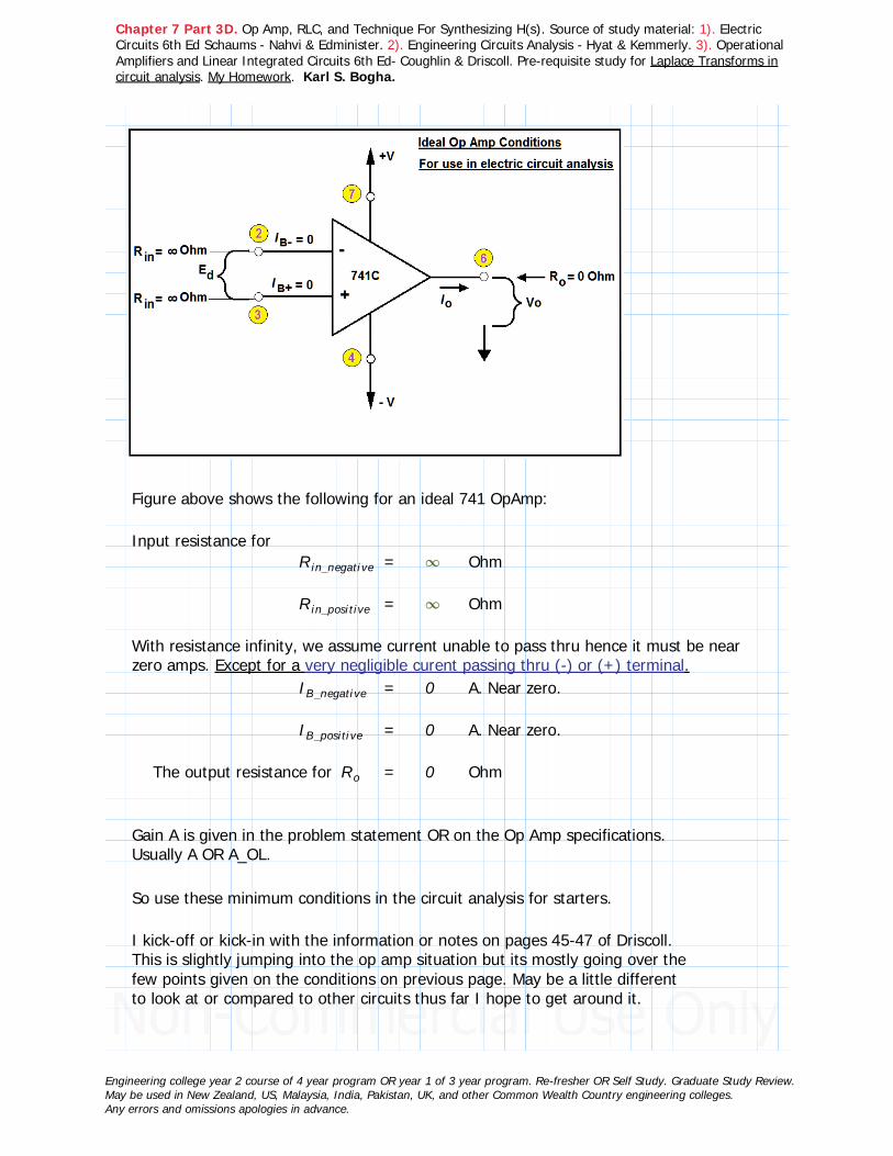
-ve terminal of Rf is connected to the node (at 6) and +ve terminal of RL is connected to node (at 6).At node 6 the (solid black dot) is the connection point identified as Vo (Output Voltage).
What is the value of this voltage?
Its the voltage measured to earth shown in next figure, ie Vo.
So voltage at the node is what is identified as Vo. Ok. Looks a little tricky at first to me.Its a device, op amp, and the output looks like an input because of the connections at the node; current coming from Rf is the input into the op amp terminal 6. The voltage at 6 causes current to flow from 0 Ref (Earth) thru RL, thats creates Vo across RL. Its a loop with the earth point in it. Electronics! So voltage across RL would be Vo. I can agree with that.
Question: When Ri is Mega Ohms, what is the +ve terminal of Rf and the -ve terminal of RL connected to?
When Ri = Mega Ohms: +ve Rf terminal connected to black node which is left of the op amp terminal number 2. Terminal '2 to 3' are at infinite resistance. Now black node is at? Virtual Earth! Ri is too high a value impeding current flow.Assume near zero current flows thru the black node and -ve terminal. See purple loop next page.
-ve RL terminal is connected to earth potential.Both +ve Rf and -ve RL connection points are at earth potential. Ok.
Engineering college year 2 course of 4 year program OR year 1 of 3 year program. Re-fresher OR Self Study. Graduate Study Review.May be used in New Zealand, US, Malaysia, India, Pakistan, UK, and other Common Wealth Country engineering colleges.Any errors and omissions apologies in advance.

Chapter 7 Part 3D. Op Amp, RLC, and Technique For Synthesizing H(s). Source of study material: 1). Electric Circuits 6th Ed Schaums - Nahvi & Edminister. 2). Engineering Circuits Analysis - Hyat & Kemmerly. 3). Operational Amplifiers and Linear Integrated Circuits 6th Ed- Coughlin & Driscoll. Pre-requisite study for Laplace Transforms in circuit analysis. My Homework. Karl S. Bogha.
Here, is the genious of the circuitry for me. First looks like a trick, or wrong.Ok for me I dont get it the first time you got it. Ri can't always be infinity preventing current to flow? That was for a circuit discussion. Yes. Got It. Examples will come.
Continuing with Ri = Mega Ohms.
The black node near terminal 2 is 0V. At virtual earth? Yes, because Ri is so high no appreciable current flow out of it. When the voltmeter leads are connected to this node and the terminal 6 node? This voltage is vRf.
Rf +ve terminal at 0 Volts and Rf -ve terminal at Vo Volts.Vo volts is some value I just identify it as Vo. Ok.
Question: Is the voltage across Rf, ie vRf, equal to voltage at the node at terminal 6?
Answer: Yes. vRf = Vo. Agreed. Which Vo was found to be equal to vRL, just before this new discovery.I call it a discovery. Why? Becaue I dont get real life cases just textbook. Funny? Hope so.Bringing in the voltage loop thing 'sum of voltages in a loop equal zero'.Usually we see it as the voltage source is +ve the remaining voltage drops negative and that sum equal zero. But why not? See figure.
The purple color loop roughly is the voltage loop. Sum of voltages equal zero.
+++Ei vRi vRF vRL = 0
For this to happen the current in Ri, Rf, and RL has to be negative. At Rf's -ve terminal the voltage would be -vRf because at this point I is at Rf's -ve terminal so its -ve? Eeeh not exactly, but if its a volt drop the voltage has to be -ve. Maybe it can be shown thru the -ve terminal of Rf...for current flow convention but must be carefull.
Engineering college year 2 course of 4 year program OR year 1 of 3 year program. Re-fresher OR Self Study. Graduate Study Review.May be used in New Zealand, US, Malaysia, India, Pakistan, UK, and other Common Wealth Country engineering colleges.Any errors and omissions apologies in advance.

Chapter 7 Part 3D. Op Amp, RLC, and Technique For Synthesizing H(s). Source of study material: 1). Electric Circuits 6th Ed Schaums - Nahvi & Edminister. 2). Engineering Circuits Analysis - Hyat & Kemmerly. 3). Operational Amplifiers and Linear Integrated Circuits 6th Ed- Coughlin & Driscoll. Pre-requisite study for Laplace Transforms in circuit analysis. My Homework. Karl S. Bogha.
+++Ei vRi vRF vRL = 0
+++Ei ⎛⎝ ⋅−I Ri⎞⎠ ⎛⎝ ⋅−I RF⎞⎠ ⎛⎝ ⋅−I RL⎞⎠ = 0
Correct? Yes I said.So basic and over looked OR making it work? Usually I start with making it work!Where does this take me? Earlier I did this below but the current was shown as +ve I.
Voltage drop across Rf:VRf = ⋅I Rf
= ⋅⎛⎜⎝―Ei
Ri
⎞⎟⎠
Rf
Actually the reference to the current sign should be -ve from our voltage loop.
VRf = ⋅−I Rf
VRf = ⋅−⎛⎜⎝―Ei
Ri
⎞⎟⎠
Rf
I know Vo = vRf. Correct, so this is the twist or turn here.
Vo = VRf Vo is the voltage at terminal 6.
Vo = ⋅−⎛⎜⎝―Ei
Ri
⎞⎟⎠
Rf
Vo = ⋅−Ei⎛⎜⎝―Rf
Ri
⎞⎟⎠
Better.
Vo has a negative sign compared to Ei. This is why this Op Amp connection is called the inverting amplifier. Polarity of output Vo is inverted compared to Ei.Discussion Aol :Now for the purpose of the amplifier gain, Acl is closed loop gain. This circuit we looked at is closed loop gain, why? I said because we got a voltage loop, you can't get it if it was open which is a straight thru connection. But all connections are closed if the circuit is to make! We have a feedback resistor Rf that helps make a closed loop? Yes!Its a closed loop because near op amp terminal 2 (-ve) is connected to the output terminal (6) with the insertion of Rf. This connection makes a closed loop. Its also called a negative feedback loop because terminal 2 is negative terminal.
Open loop gain Aol = Vo/Ed. OR Vo = Open Loop Gain A_OL x Differential Voltage Ed.Ed is the voltage between terminal 2 and 3. Aol is without Rf feedback.
Engineering college year 2 course of 4 year program OR year 1 of 3 year program. Re-fresher OR Self Study. Graduate Study Review.May be used in New Zealand, US, Malaysia, India, Pakistan, UK, and other Common Wealth Country engineering colleges.Any errors and omissions apologies in advance.

Chapter 7 Part 3D. Op Amp, RLC, and Technique For Synthesizing H(s). Source of study material: 1). Electric Circuits 6th Ed Schaums - Nahvi & Edminister. 2). Engineering Circuits Analysis - Hyat & Kemmerly. 3). Operational Amplifiers and Linear Integrated Circuits 6th Ed- Coughlin & Driscoll. Pre-requisite study for Laplace Transforms in circuit analysis. My Homework. Karl S. Bogha.
ACL is the closed loop gain. ACL = ―Vo
EiEi is Vi. If there was an external resistor R1 after Ei, before the node to Rf, the voltage at what was the black connection would be called v1 or something else. Correct that thought dependent on circuit. Examples will follow.
SinceVo = ⋅−Ei
⎛⎜⎝―Rf
Ri
⎞⎟⎠
ACL = ―Vo
Ei= ――――
⋅−Ei⎛⎜⎝―Rf
Ri
⎞⎟⎠
Ei
ACL = −⎛⎜⎝―Rf
Ri
⎞⎟⎠
Current flow into the node shown at near output terminal 6: Question what is Io?
In the voltage loop analysis I agreed the current was -I. So it made the sum of voltages equal zero.Sum of currents at node must equal? Zero.Tricky thing is how to set the 'current direction on I_L' the load current flowing thru resistor RL. And is current Io flowing into terminal 6? Yes for the inverting opamp.Voltage across RL is Vo.Voltage across Rf is Vo.
Discussion:
Since voltage across both the feedback resistors Rf and RL are the same, Vo of the same polarity, would current flow in the same direction for both the resistors?
No, its dependent on circuit connection conditions. We cannot say because the voltage is the same across Rf and RL the current flow direction is the same.
Figure to the left exaplained next page. SEE NEXT FIGURE.
Engineering college year 2 course of 4 year program OR year 1 of 3 year program. Re-fresher OR Self Study. Graduate Study Review.May be used in New Zealand, US, Malaysia, India, Pakistan, UK, and other Common Wealth Country engineering colleges.Any errors and omissions apologies in advance.

Chapter 7 Part 3D. Op Amp, RLC, and Technique For Synthesizing H(s). Source of study material: 1). Electric Circuits 6th Ed Schaums - Nahvi & Edminister. 2). Engineering Circuits Analysis - Hyat & Kemmerly. 3). Operational Amplifiers and Linear Integrated Circuits 6th Ed- Coughlin & Driscoll. Pre-requisite study for Laplace Transforms in circuit analysis. My Homework. Karl S. Bogha.
Follow the current path from the voltage source Ei.
Here I can see the current entering thru the bottom side of the resistor RL.This solves my mystery on why and how the current was flowing into the node from the RL connection.Rf and RL are in parallel.<--- See circuit to the left turned 90 degs for better current flow comparison.
In my circuit I show voltage across 'Rf and RL' equal because they are parallel.
The yellow shaded area shows Io.Follow the current flow, red arrows, it solves the RL situation voltage is Vo. Rf and RL are in a parallel connection with each other, one end connected to terminal 6 where the voltage is Vo, the other to earth potential 0V. Next its merely fixing the signs on I and IL, relative to Io which is the output current. The arrows show currents going into Io. Correct. Convention here for currents entering node -ve and leaving node +ve. Current direction in this circuit is really input to 6, but we call it output because of the terminal location 6, its just the -ve sign on Io. Later we see a +ve Io.
What the op amp results with is a gain, Vo/Ei. Initially it may look like current is leaving terminal 6, actually its entering. Voltage across RL now is more realisable/acceptable from figure above. Through this, entering Io, the op amp is able to generate a higher voltage at the output terminal 6 which here is identified as Vo.
Sum of current at node:++IO ((−I)) ⎛⎝−IL⎞⎠ = 0
IO = +I IL <---- Correct. In the inverting opam.
What is Io? Io is the output current here entering terminal 6 into the Op Amp.
This brings me to an end to this topic. Next some simple examples.Apologies for any error and omissions.
Engineering college year 2 course of 4 year program OR year 1 of 3 year program. Re-fresher OR Self Study. Graduate Study Review.May be used in New Zealand, US, Malaysia, India, Pakistan, UK, and other Common Wealth Country engineering colleges.Any errors and omissions apologies in advance.

Chapter 7 Part 3D. Op Amp, RLC, and Technique For Synthesizing H(s). Source of study material: 1). Electric Circuits 6th Ed Schaums - Nahvi & Edminister. 2). Engineering Circuits Analysis - Hyat & Kemmerly. 3). Operational Amplifiers and Linear Integrated Circuits 6th Ed- Coughlin & Driscoll. Pre-requisite study for Laplace Transforms in circuit analysis. My Homework. Karl S. Bogha.
Example 1 (C&D - Coughlin and Driscoll):
For the circuit on left.Calculate a). I b). Vo c). A_CL closed
loop gain Note: Ei is a dc voltage source.This is an inverting opam circuit because Ei is connected to the -ve terminal and +ve to earth 0V potential. Because its at 0V it does not mean current will not flow thru to the other conductors at that point. 0V Ref is near zero or 0, at that point current will flow past,because of the pull by other circuit components, closed circuit connection of the circuit, and the supply from the voltage source.
Solution:
I = ―Ei
Ri≔Ei 1 V ≔Ri ⋅10 103 Ohm
I = =―Ei
Ri⋅1 10−4 = ⋅0.1 10−3 = 0.1 mA. Answer.
Vo = ⋅−Ei⎛⎜⎝―Rf
Ri
⎞⎟⎠
≔Rf ⋅100 103 Ohm
Vo = =⋅−Ei⎛⎜⎝―Rf
Ri
⎞⎟⎠−10
Vo = −10 V Answer.
ACL = =−⎛⎜⎝―Rf
Ri
⎞⎟⎠−10
ACL = −10 Gain. Answer.
Comments:Nice simple example, got Op Amp started!Calculated the gain based on resistor values. I hope that got most of the confusion out I admit there was for me. On previous notes did I really need to emphasise an infinity resistance at the black node with near 0 current flow.....? Maybe the textbook idea was how to form the equations based on voltage and ignoring current for a while.
Engineering college year 2 course of 4 year program OR year 1 of 3 year program. Re-fresher OR Self Study. Graduate Study Review.May be used in New Zealand, US, Malaysia, India, Pakistan, UK, and other Common Wealth Country engineering colleges.Any errors and omissions apologies in advance.

Chapter 7 Part 3D. Op Amp, RLC, and Technique For Synthesizing H(s). Source of study material: 1). Electric Circuits 6th Ed Schaums - Nahvi & Edminister. 2). Engineering Circuits Analysis - Hyat & Kemmerly. 3). Operational Amplifiers and Linear Integrated Circuits 6th Ed- Coughlin & Driscoll. Pre-requisite study for Laplace Transforms in circuit analysis. My Homework. Karl S. Bogha.
Example 2 (C&D - Coughlin and Driscoll):
For the circuit to the left, similar to example 1, with RL value added for 25 k Ohm.
Determine:a). IL
b). Total current into the output pin, 6, of the op amp.
Note: Ei is a dc voltage source.
Solution:
Vo calculated in example 1:≔Vo −10 V
I_L:IL = ――
Vo
RL
≔RL ⋅25 103 k ohm
≔IL =――Vo
RL−0.0004 = ⋅−0.4 10−3 = −0.4 mA. Answer.
Negative value for currentas we desire.Io :
++IO I IL = 0
I value assigned the -ve sign relative to Vo polarity: I = −0.1 mA
++IO ((−1 mA)) ((−0.4 mA)) = 0
−IO 0.5 mA = 0
IO = 0.5 mA Answer. <--- Entering node.C&D comments: Io usually is between 5 mA and 10 mA. Instrumentation circuits operate at 5-20mA.Input resistance seen by Ei is Ri. In order to keep the input resistance high, Ri must be 10 k ohm or higher.
Engineering college year 2 course of 4 year program OR year 1 of 3 year program. Re-fresher OR Self Study. Graduate Study Review.May be used in New Zealand, US, Malaysia, India, Pakistan, UK, and other Common Wealth Country engineering colleges.Any errors and omissions apologies in advance.
Chapter 7 Part 3D. Op Amp, RLC, and Technique For Synthesizing H(s). Source of study material: 1). Electric Circuits 6th Ed Schaums - Nahvi & Edminister. 2). Engineering Circuits Analysis - Hyat & Kemmerly. 3). Operational Amplifiers and Linear Integrated Circuits 6th Ed- Coughlin & Driscoll. Pre-requisite study for Laplace Transforms in circuit analysis. My Homework. Karl S. Bogha.
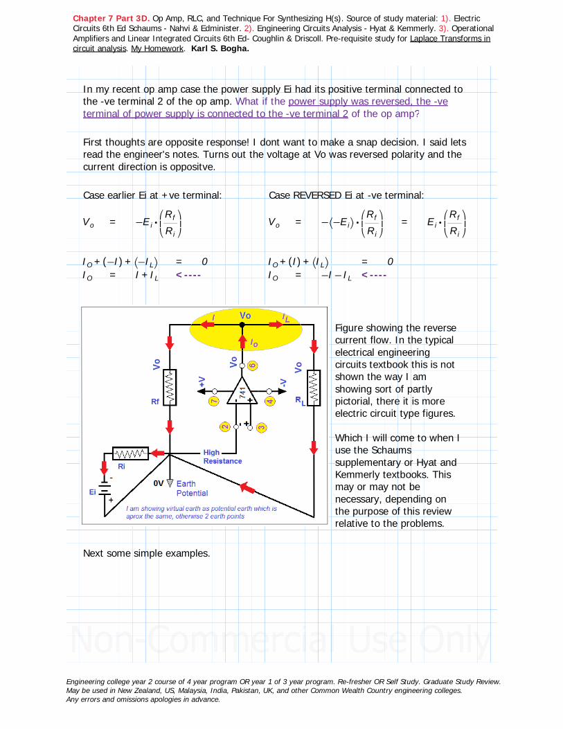
In my recent op amp case the power supply Ei had its positive terminal connected to the -ve terminal 2 of the op amp. What if the power supply was reversed, the -ve terminal of power supply is connected to the -ve terminal 2 of the op amp?
First thoughts are opposite response! I dont want to make a snap decision. I said lets read the engineer's notes. Turns out the voltage at Vo was reversed polarity and the current direction is oppositve.
Case earlier Ei at +ve terminal: Case REVERSED Ei at -ve terminal:
Vo = ⋅−Ei⎛⎜⎝―Rf
Ri
⎞⎟⎠
Vo = ⋅−⎛⎝−Ei⎞⎠⎛⎜⎝―Rf
Ri
⎞⎟⎠
= ⋅Ei⎛⎜⎝―Rf
Ri
⎞⎟⎠
++IO ((−I)) ⎛⎝−IL⎞⎠ = 0 ++IO ((I)) ⎛⎝IL⎞⎠ = 0IO = +I IL <---- IO = −−I IL <----
Figure showing the reverse current flow. In the typical electrical engineering circuits textbook this is not shown the way I am showing sort of partly pictorial, there it is more electric circuit type figures.
Which I will come to when I use the Schaums supplementary or Hyat and Kemmerly textbooks. This may or may not be necessary, depending on the purpose of this review relative to the problems.
Next some simple examples.
Engineering college year 2 course of 4 year program OR year 1 of 3 year program. Re-fresher OR Self Study. Graduate Study Review.May be used in New Zealand, US, Malaysia, India, Pakistan, UK, and other Common Wealth Country engineering colleges.Any errors and omissions apologies in advance.

Chapter 7 Part 3D. Op Amp, RLC, and Technique For Synthesizing H(s). Source of study material: 1). Electric Circuits 6th Ed Schaums - Nahvi & Edminister. 2). Engineering Circuits Analysis - Hyat & Kemmerly. 3). Operational Amplifiers and Linear Integrated Circuits 6th Ed- Coughlin & Driscoll. Pre-requisite study for Laplace Transforms in circuit analysis. My Homework. Karl S. Bogha.
Example 3 (C&D - Coughlin and Driscoll):
Note: Ei is a dc voltage source.Caution: This example I worked it wrong first. Then forced my solution to the Engineers. It made sense, because the emphasis was on establishing the voltage as the path to the solutionrather than the correct sign of the current direction. Just as the theory was developed.Fear not it gets easier along the way.
Let Rf = 250 kohm, Ri = 10 kohm, and Ei = -0.5V.Calculate a). I b). the voltage across Rf c). Vo
Discussion: Current would been -0.05mA when Ei was plugged in at -0.5V. However, the configuration of the circuit to the opam takes precedence. If the Ei is +ve, Vo is -ve for inverting opamp. The current is merely used to multiply resistance to get a voltage.
Solution:
≔Ei −0.5 V ≔Ri ⋅10 103 OhmMy first attempt of course Ei=-0.5V.Engineers got +0.5V? Formula strictly wrt voltage. I made it -0.5V to match current flow's opposite direction. Maybe why I said we used voltage for reference with current near zero from high resistance.
I = =――−0.5
Ri⋅−5 10−5= ⋅−0.05 10−3= −0.05
Not Correct.
I = =――0.5Ri
⋅5 10−5 = ⋅0.05 10−3 = 0.05 mA. Answer. Without setting the current direction relative to Ei polarity.
vRf = ⋅I Rf ≔Rf ⋅250 103 Using I as 0.05 mA
vRf = =⋅⋅0.05 10−3 Rf 12.5 V Answer.
Vo = =⋅−Ei⎛⎜⎝―Rf
Ri
⎞⎟⎠
12.5 Answer. With Ei set equal to = - 0.5V because its a voltage formula it takes precedence, as I said keeping it voltage priority.
Voltage magnitude across Rf equal the opamp output voltage Vo ie 12.5V.
What will Acl, gain, equal? ACL = =−⎛⎜⎝―Rf
Ri
⎞⎟⎠−25 Correct. Answer.
Engineering college year 2 course of 4 year program OR year 1 of 3 year program. Re-fresher OR Self Study. Graduate Study Review.May be used in New Zealand, US, Malaysia, India, Pakistan, UK, and other Common Wealth Country engineering colleges.Any errors and omissions apologies in advance.

Chapter 7 Part 3D. Op Amp, RLC, and Technique For Synthesizing H(s). Source of study material: 1). Electric Circuits 6th Ed Schaums - Nahvi & Edminister. 2). Engineering Circuits Analysis - Hyat & Kemmerly. 3). Operational Amplifiers and Linear Integrated Circuits 6th Ed- Coughlin & Driscoll. Pre-requisite study for Laplace Transforms in circuit analysis. My Homework. Karl S. Bogha.
Example 4 (C&D - Coughlin and Driscoll):
Note: Ei is a dc voltage source.
Same values as in Example 3. Continuation.Let Rf = 250 kohm, Ri = 10 kohm, and Ei = -0.5V.Calculate a). RL for a load current of 2 mA? b). Io c). Circuit input resistance RiSolution:
What do we know about RL?
Voltage across RL equal Vo.Current thru RL is given 2mA.I may apply Ohm's expression to find RL.
≔Vo 12.5 ≔IRL ⋅2 10−3 A
≔RL =――Vo
IRL⋅6.25 103 RL = 6.25 k Ohm Answer.
Io = I + I_L. I was calculated in example 3 and it was 0.05 mA.
≔I 0.05 mA ≔IL 2 mA ≔IO =+I IL 2.05 mA Answer.
Input resistance Ri is given in the problem statement = 10 k Ohm. Answer.
Discussion: The current flow the way I see it, matching solution, use voltage as the benchmark and in the inverting opamp I and IL enter the opamp into terminal 6.
Engineering college year 2 course of 4 year program OR year 1 of 3 year program. Re-fresher OR Self Study. Graduate Study Review.May be used in New Zealand, US, Malaysia, India, Pakistan, UK, and other Common Wealth Country engineering colleges.Any errors and omissions apologies in advance.

Chapter 7 Part 3D. Op Amp, RLC, and Technique For Synthesizing H(s). Source of study material: 1). Electric Circuits 6th Ed Schaums - Nahvi & Edminister. 2). Engineering Circuits Analysis - Hyat & Kemmerly. 3). Operational Amplifiers and Linear Integrated Circuits 6th Ed- Coughlin & Driscoll. Pre-requisite study for Laplace Transforms in circuit analysis. My Homework. Karl S. Bogha.
Voltage Applied To The Inverting Input.
I had a dc voltage supply now I have an ac voltage supply. And its called ac signal voltage Ei. Its not acting like a power supply for a lamp or fan or heater, its more for a signal to the op amp. Signal? The way I see it, I intepret it as an input waveform that is going to be processed by the circuit. Maybe you ask your lecturer why in the EE textbooks they commonly identify the source as a signal something, here ac signal source Ei. Its a signal which is part power of course but its going to be processed as an input signal in a circuit for a desired signal output. Its not part power because no work like motor or pump work is expected from it.
For the circuit below the ac signal source has a cycle, a positive side for one half cycle, and a negative side for the other half cycle.
The two circuits I seen, or we seen, with the positive and negative polarity connection to terminal 2 can be applied here in combination.
Positive connection for the positive half ac signal.Negative connection for the negative half ac signal.
From the past examples its known when:Ei is a positive connection to terminal 2, Vo is negative,Ei is a negative connection to terminal 2, Vo is positive.
Vo = ⋅−⎛⎝Ei⎞⎠⎛⎜⎝―Ri
Rf
⎞⎟⎠
Positive connection to terminal 2, triangular ac waveform voltage supply.
Next 2 simple examples, with some input and output waveforms to match up to the answers.
Engineering college year 2 course of 4 year program OR year 1 of 3 year program. Re-fresher OR Self Study. Graduate Study Review.May be used in New Zealand, US, Malaysia, India, Pakistan, UK, and other Common Wealth Country engineering colleges.Any errors and omissions apologies in advance.

Chapter 7 Part 3D. Op Amp, RLC, and Technique For Synthesizing H(s). Source of study material: 1). Electric Circuits 6th Ed Schaums - Nahvi & Edminister. 2). Engineering Circuits Analysis - Hyat & Kemmerly. 3). Operational Amplifiers and Linear Integrated Circuits 6th Ed- Coughlin & Driscoll. Pre-requisite study for Laplace Transforms in circuit analysis. My Homework. Karl S. Bogha.
Example 5 (C&D):
For the circuit above, Rf = 20 kohm, and Ri = 10 kohm.Calculate the voltage gain Acl ?Solution:≔Rf ⋅20 103 ≔Ri ⋅10 103 ACL = =−
⎛⎜⎝―Rf
Ri
⎞⎟⎠−2 Answer.
Example 6 (C&D):Continuing from example 5.If the input voltage is -5V. Deterimine the output voltage.
Solution:≔Ei −5 V ≔Ri ⋅10 103 ≔Rf ⋅20 103
Vo = =⋅−⎛⎝Ei⎞⎠⎛⎜⎝―Rf
Ri⎞⎟⎠
10 Answer.Voltage expression.
Simple graph, Vo is twice Ei, on the vertical axis, with time t on the horizontal axis --->
The result is saying the output should have a gain of 2 compared to the input. This can be shown on a graph. As would be expected on the oscilloscope screen.At time t=0, Vo/Ei? From the graph.
≔Vo 10 ≔Ei −5 ≔ACL =―Vo
Ei−2
So the graph shows the same -2 at t=0.Vo = -5 x -2 = 10 at t=0.
Engineering college year 2 course of 4 year program OR year 1 of 3 year program. Re-fresher OR Self Study. Graduate Study Review.May be used in New Zealand, US, Malaysia, India, Pakistan, UK, and other Common Wealth Country engineering colleges.Any errors and omissions apologies in advance.

Chapter 7 Part 3D. Op Amp, RLC, and Technique For Synthesizing H(s). Source of study material: 1). Electric Circuits 6th Ed Schaums - Nahvi & Edminister. 2). Engineering Circuits Analysis - Hyat & Kemmerly. 3). Operational Amplifiers and Linear Integrated Circuits 6th Ed- Coughlin & Driscoll. Pre-requisite study for Laplace Transforms in circuit analysis. My Homework. Karl S. Bogha.
I want to continue on with the material from C&D but maybe better I get to the inverting amplifier first also in C&D. Then get to Schaums for some electric circuit type environment. My guess same as yours will it be the same! Should be.
Inverting op amp the connections of the voltage signal was at terminal 2,but for non-inverting opamp now its to terminal 3.
The op amp is 177 not 741. Here the input voltage signal is applied to terminal 3.Terminal 2 is high resistance. Current Ia = 0 because of the high resistance, some negligible current is flowing thru but its not considered.
The node connection Ri and Rf, has a branch to 2 which has zero current.That makes the connection to Ri and Rf a series connection. Otherwise if there was current in Ia it would be a parallel. Agreed. Seen this in the 741 circuiting on the earth potential.
I = ―Ei
RiVRi = Ei VRf = ⋅I Rf =
⎛⎜⎝―Ei
Ri⎞⎟⎠
Rf= Ei⎛⎜⎝――RfRi⎞⎟⎠V_Ri and Ei are parallel.
Vo = +VRi VRf = +Ei Ei⎛⎜⎝――RfRi⎞⎟⎠
= ⎛⎜⎝
+1 ――RfRi⎞⎟⎠
Ei
Engineering college year 2 course of 4 year program OR year 1 of 3 year program. Re-fresher OR Self Study. Graduate Study Review.May be used in New Zealand, US, Malaysia, India, Pakistan, UK, and other Common Wealth Country engineering colleges.Any errors and omissions apologies in advance.
Chapter 7 Part 3D. Op Amp, RLC, and Technique For Synthesizing H(s). Source of study material: 1). Electric Circuits 6th Ed Schaums - Nahvi & Edminister. 2). Engineering Circuits Analysis - Hyat & Kemmerly. 3). Operational Amplifiers and Linear Integrated Circuits 6th Ed- Coughlin & Driscoll. Pre-requisite study for Laplace Transforms in circuit analysis. My Homework. Karl S. Bogha.
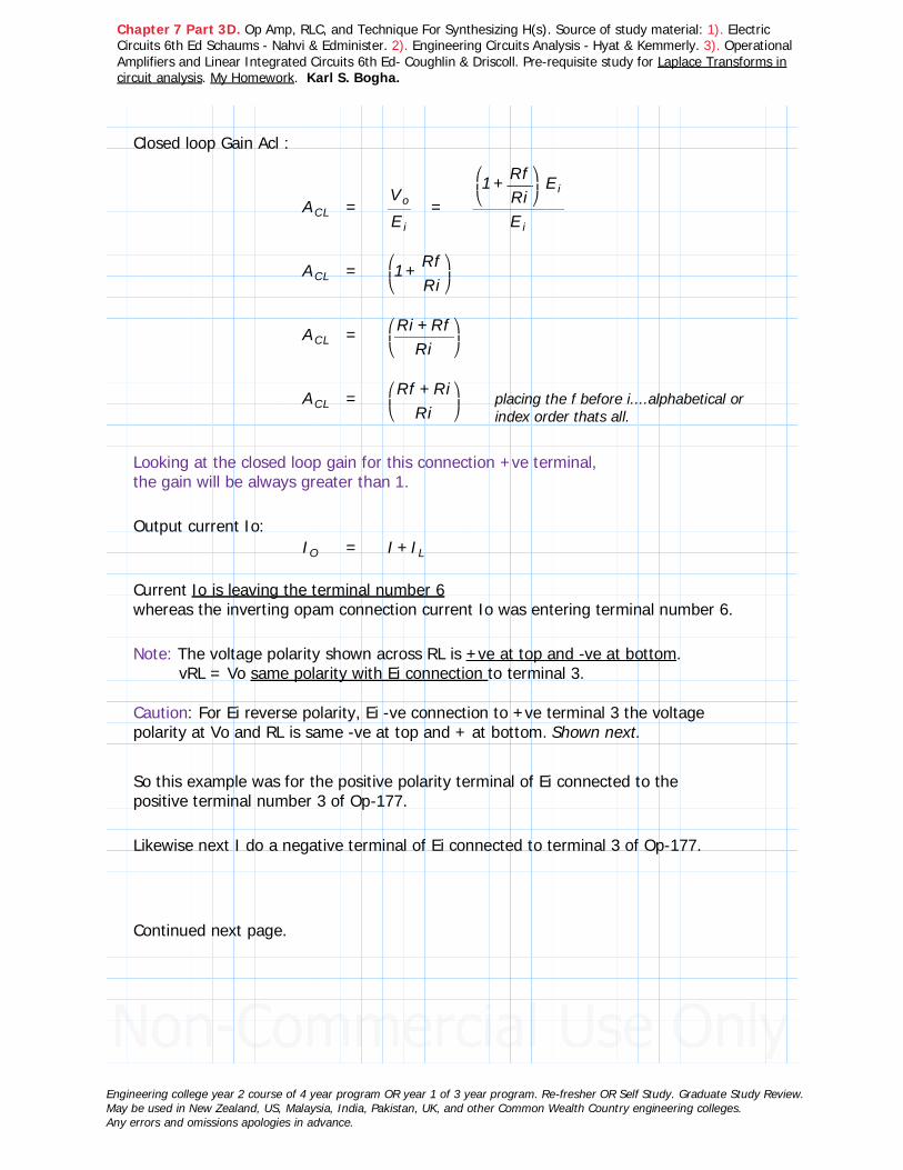
Closed loop Gain Acl :
ACL = ―Vo
Ei= ――――
⎛⎜⎝
+1 ――RfRi⎞⎟⎠
Ei
Ei
ACL = ⎛⎜⎝
+1 ――RfRi⎞⎟⎠
ACL = ⎛⎜⎝―――
+Ri RfRi
⎞⎟⎠
ACL = ⎛⎜⎝―――
+Rf RiRi
⎞⎟⎠
placing the f before i....alphabetical or index order thats all.
Looking at the closed loop gain for this connection +ve terminal, the gain will be always greater than 1.
Output current Io:IO = +I IL
Current Io is leaving the terminal number 6 whereas the inverting opam connection current Io was entering terminal number 6.
Note: The voltage polarity shown across RL is +ve at top and -ve at bottom.vRL = Vo same polarity with Ei connection to terminal 3.
Caution: For Ei reverse polarity, Ei -ve connection to +ve terminal 3 the voltage polarity at Vo and RL is same -ve at top and + at bottom. Shown next.
So this example was for the positive polarity terminal of Ei connected to thepositive terminal number 3 of Op-177.
Likewise next I do a negative terminal of Ei connected to terminal 3 of Op-177.
Continued next page.
Engineering college year 2 course of 4 year program OR year 1 of 3 year program. Re-fresher OR Self Study. Graduate Study Review.May be used in New Zealand, US, Malaysia, India, Pakistan, UK, and other Common Wealth Country engineering colleges.Any errors and omissions apologies in advance.

Chapter 7 Part 3D. Op Amp, RLC, and Technique For Synthesizing H(s). Source of study material: 1). Electric Circuits 6th Ed Schaums - Nahvi & Edminister. 2). Engineering Circuits Analysis - Hyat & Kemmerly. 3). Operational Amplifiers and Linear Integrated Circuits 6th Ed- Coughlin & Driscoll. Pre-requisite study for Laplace Transforms in circuit analysis. My Homework. Karl S. Bogha.
Calculating the variables/parameters is the same as the previous figure's information.
Output current Io:IO = +I IL
Current Io is entering the terminal number 6.
Note: The voltage polarity shown across RL is -ve at top and +ve at bottom.vRL = Vo same polarity with Ei connection to terminal 3.
What Ei polarity connection is thats the same at Vo. See formula in figure above.
Next some simple examples.
Comment:There is more content in the C&D textbook here in these chapters than found in the electronic textbooks application wise. But for my circuits purpose 'the external connections terminals of op amp to the other circuit components'. I will try to keep it in this objective so it helps make working and understanding the Schaums electric circuits example problems.
Engineering college year 2 course of 4 year program OR year 1 of 3 year program. Re-fresher OR Self Study. Graduate Study Review.May be used in New Zealand, US, Malaysia, India, Pakistan, UK, and other Common Wealth Country engineering colleges.Any errors and omissions apologies in advance.

Chapter 7 Part 3D. Op Amp, RLC, and Technique For Synthesizing H(s). Source of study material: 1). Electric Circuits 6th Ed Schaums - Nahvi & Edminister. 2). Engineering Circuits Analysis - Hyat & Kemmerly. 3). Operational Amplifiers and Linear Integrated Circuits 6th Ed- Coughlin & Driscoll. Pre-requisite study for Laplace Transforms in circuit analysis. My Homework. Karl S. Bogha.
Example 7 (C&D):
Find the voltage gain for the non-inverting amplifier (shown in the circuit above) ?
If Ei is a 100 Hz triangular wave with a 2V peak.
Plot:
a). Vo vs t
b). Vo vs Ei
Solution:
From previous notes the voltage gain expression is:
≔Ri ⋅10 103
≔Rf ⋅40 103
ACL =⎛⎜⎝―――
+Rf Ri
Ri
⎞⎟⎠
= =⎛⎜⎝―――
+Rf Ri
Ri
⎞⎟⎠
5 Answer. Gain of 5.
Engineering college year 2 course of 4 year program OR year 1 of 3 year program. Re-fresher OR Self Study. Graduate Study Review.May be used in New Zealand, US, Malaysia, India, Pakistan, UK, and other Common Wealth Country engineering colleges.Any errors and omissions apologies in advance.

Chapter 7 Part 3D. Op Amp, RLC, and Technique For Synthesizing H(s). Source of study material: 1). Electric Circuits 6th Ed Schaums - Nahvi & Edminister. 2). Engineering Circuits Analysis - Hyat & Kemmerly. 3). Operational Amplifiers and Linear Integrated Circuits 6th Ed- Coughlin & Driscoll. Pre-requisite study for Laplace Transforms in circuit analysis. My Homework. Karl S. Bogha.
Next part of the solution may look like where do I start.That was my reaction.
I got the Vo expression with Acl and Ei. This is shown in the circuit figure.I wrote it in. Yes, I had some idea on Acl, but I did not know that my plot was going to be from that expression.
Acl = 5
Ei_peak = 2 V
ACL = ―Vo
Ei
Vo = ⋅Acl Ei_peak = =⋅5 2 10 V
Vo = 10 V
≔f 100 Wave frequency.
≔T =―1f
0.01 = ――1100
= ――10
1000= 10 ms - millisecond
Plot of Ei Vs t.Triangle wave has a period of 10 ms.Likewise the output will have the same frequency, based on the input signal, so it has the same period.
Continued next page.
Engineering college year 2 course of 4 year program OR year 1 of 3 year program. Re-fresher OR Self Study. Graduate Study Review.May be used in New Zealand, US, Malaysia, India, Pakistan, UK, and other Common Wealth Country engineering colleges.Any errors and omissions apologies in advance.

Chapter 7 Part 3D. Op Amp, RLC, and Technique For Synthesizing H(s). Source of study material: 1). Electric Circuits 6th Ed Schaums - Nahvi & Edminister. 2). Engineering Circuits Analysis - Hyat & Kemmerly. 3). Operational Amplifiers and Linear Integrated Circuits 6th Ed- Coughlin & Driscoll. Pre-requisite study for Laplace Transforms in circuit analysis. My Homework. Karl S. Bogha.
Plot of Vo vs t in purplewith the plot of Ei vs t in blue.
Next plot is Vo vs Ei.
How do I do that?Vo on y axis and Eo on x axis.Here there is no time t.
<--- Form the data for the plot from the plot to the left.
E1 Vo
−2 −10
0 0
2 10
The plot sought.Its a straight line, linear.As the gain is 2 this is expected for Vo Vs Ei.Obviously the line should not exceed Ei = 2 because the peak of Ei is 2V.
I like to carry on with C&D textbook but I have to jump to Schaums.Start from the begining, again, but in the circuits approach. Maybe have a revisit on some content as I go along from C&D.
Engineering college year 2 course of 4 year program OR year 1 of 3 year program. Re-fresher OR Self Study. Graduate Study Review.May be used in New Zealand, US, Malaysia, India, Pakistan, UK, and other Common Wealth Country engineering colleges.Any errors and omissions apologies in advance.

Chapter 7 Part 3D. Op Amp, RLC, and Technique For Synthesizing H(s). Source of study material: 1). Electric Circuits 6th Ed Schaums - Nahvi & Edminister. 2). Engineering Circuits Analysis - Hyat & Kemmerly. 3). Operational Amplifiers and Linear Integrated Circuits 6th Ed- Coughlin & Driscoll. Pre-requisite study for Laplace Transforms in circuit analysis. My Homework. Karl S. Bogha.
Starting with Schaums Chapter 5 of 6th edition.
What the engineers said in the preface of this edition:
The opamp examples and problems in Chapter 5 were selected carefully to illustrate simple but practical cases which are of interest and importance to the future courses.
My comment is the examples in the theory section, and those in the solved examples and unsolved problems are closer to their applications in signal processing and controls courses. The internal side of the design of the opamp thats the electronic course(s). So obviously this component is critical since it plays a role in so many courses and applications. I am interested in the electric circuits side of things; applying it in a circuit.
Electric Circuits courses do not usually take on opamp circuit as a main topic. Fortunately in Schaums 6th edition has a chapter devoted. Thats not because there is a conspiracy, electric circuits typically focus or concern with RLC components. Then in the electronic course opamps are introduced. Time may be a factor to devote a whole major topic to it.
My Plan:
I will do the whole theory of the chapter with the examples in the theory section.
Continued next page.
Engineering college year 2 course of 4 year program OR year 1 of 3 year program. Re-fresher OR Self Study. Graduate Study Review.May be used in New Zealand, US, Malaysia, India, Pakistan, UK, and other Common Wealth Country engineering colleges.Any errors and omissions apologies in advance.
Chapter 7 Part 3D. Op Amp, RLC, and Technique For Synthesizing H(s). Source of study material: 1). Electric Circuits 6th Ed Schaums - Nahvi & Edminister. 2). Engineering Circuits Analysis - Hyat & Kemmerly. 3). Operational Amplifiers and Linear Integrated Circuits 6th Ed- Coughlin & Driscoll. Pre-requisite study for Laplace Transforms in circuit analysis. My Homework. Karl S. Bogha.
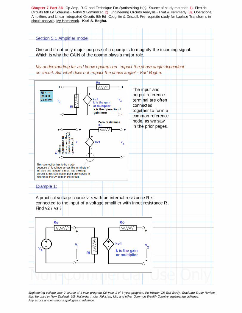
Section 5.1 Amplifier model
One and if not only major purpose of a opamp is to magnify the incoming signal. Which is why the GAIN of the opamp plays a major role.
My understanding far as I know opamp can impact the phase angle dependent on circuit. But what does not impact the phase angle! - Karl Bogha.
The input and output reference terminal are often connected together to form a common reference node, as we saw in the prior pages.
Example 1:
A practical voltage source v_s with an internal resistance R_s connected to the input of a voltage amplifier with input resistance Ri. Find v2 / vs ?
Engineering college year 2 course of 4 year program OR year 1 of 3 year program. Re-fresher OR Self Study. Graduate Study Review.May be used in New Zealand, US, Malaysia, India, Pakistan, UK, and other Common Wealth Country engineering colleges.Any errors and omissions apologies in advance.
Chapter 7 Part 3D. Op Amp, RLC, and Technique For Synthesizing H(s). Source of study material: 1). Electric Circuits 6th Ed Schaums - Nahvi & Edminister. 2). Engineering Circuits Analysis - Hyat & Kemmerly. 3). Operational Amplifiers and Linear Integrated Circuits 6th Ed- Coughlin & Driscoll. Pre-requisite study for Laplace Transforms in circuit analysis. My Homework. Karl S. Bogha.
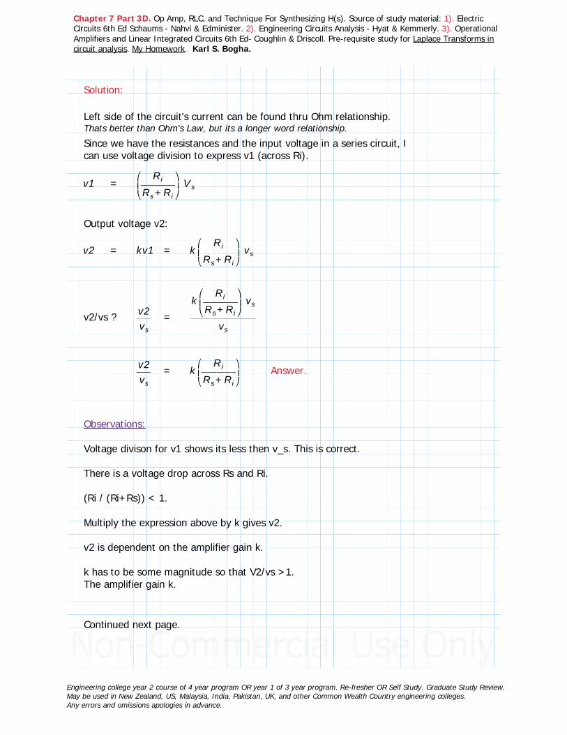
Solution:
Left side of the circuit's current can be found thru Ohm relationship.Thats better than Ohm's Law, but its a longer word relationship. Since we have the resistances and the input voltage in a series circuit, I can use voltage division to express v1 (across Ri).
v1 =⎛⎜⎝―――
Ri
+Rs Ri
⎞⎟⎠
Vs
Output voltage v2:
v2 = kv1 = k⎛⎜⎝―――
Ri
+Rs Ri
⎞⎟⎠
vs
v2/vs ? ―v2vs
= ―――――
k⎛⎜⎝―――
Ri
+Rs Ri
⎞⎟⎠
vs
vs
―v2vs
= k⎛⎜⎝―――
Ri
+Rs Ri
⎞⎟⎠
Answer.
Observations:
Voltage divison for v1 shows its less then v_s. This is correct.
There is a voltage drop across Rs and Ri.
(Ri / (Ri+Rs)) < 1.
Multiply the expression above by k gives v2.
v2 is dependent on the amplifier gain k.
k has to be some magnitude so that V2/vs >1. The amplifier gain k.
Continued next page.
Engineering college year 2 course of 4 year program OR year 1 of 3 year program. Re-fresher OR Self Study. Graduate Study Review.May be used in New Zealand, US, Malaysia, India, Pakistan, UK, and other Common Wealth Country engineering colleges.Any errors and omissions apologies in advance.

Chapter 7 Part 3D. Op Amp, RLC, and Technique For Synthesizing H(s). Source of study material: 1). Electric Circuits 6th Ed Schaums - Nahvi & Edminister. 2). Engineering Circuits Analysis - Hyat & Kemmerly. 3). Operational Amplifiers and Linear Integrated Circuits 6th Ed- Coughlin & Driscoll. Pre-requisite study for Laplace Transforms in circuit analysis. My Homework. Karl S. Bogha.
Example 2:
Given in circuit the input and output resistances, Ri and Ro, voltage source resistance Rs, and load resistance RL.
Find v2 / vs ?
Solution:Voltage on the right side of the circuit is kv1.I found kv1 from the previous example with the same resistors.Now I need to adjust for Ro and RL.Lets say I focus on the right side series circuit.Voltage across RL equal v2.Using voltage division for a series circuit:
v2 = ⎛⎜⎝―――
RL+Ro RL
⎞⎟⎠
kv1
Previous example: kv1 = k⎛⎜⎝―――
Ri
+Rs Ri
⎞⎟⎠
vs
Substitute kv1 into v2:
v2 = ⎛⎜⎝―――
RL+Ro RL
⎞⎟⎠
k⎛⎜⎝―――
Ri
+Rs Ri
⎞⎟⎠
vs
v2 = ⎛⎜⎝―――
RL+Ro RL
⎞⎟⎠
⎛⎜⎝―――
Ri
+Rs Ri
⎞⎟⎠
kvs
―v2vs
= ⋅⎛⎜⎝―――
RL+Ro RL
⎞⎟⎠
⎛⎜⎝―――
Ri
+Rs Ri
⎞⎟⎠
k Answer.
Observations:The expression v2/v_s magnitude is dependent on:1. Smaller the value of v_s larger the gain (v2/v_s) for the circuit.2. Additional resistance expression (RL/ Ro+RL) decreases the gain (RHS of equation).
Engineering college year 2 course of 4 year program OR year 1 of 3 year program. Re-fresher OR Self Study. Graduate Study Review.May be used in New Zealand, US, Malaysia, India, Pakistan, UK, and other Common Wealth Country engineering colleges.Any errors and omissions apologies in advance.
Chapter 7 Part 3D. Op Amp, RLC, and Technique For Synthesizing H(s). Source of study material: 1). Electric Circuits 6th Ed Schaums - Nahvi & Edminister. 2). Engineering Circuits Analysis - Hyat & Kemmerly. 3). Operational Amplifiers and Linear Integrated Circuits 6th Ed- Coughlin & Driscoll. Pre-requisite study for Laplace Transforms in circuit analysis. My Homework. Karl S. Bogha.
Section 5.2 Feedback in amplifier circuits
When part of the current of the opamp output is fedback into the opamp input side of the circuit this may/can raise the output voltage. This feedback path of the circuit will help make the open circuit, without feedback, gain less sensitive to variations in k (k being the open circuit gain).
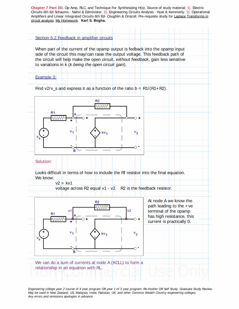
Example 3:
Find v2/v_s and express it as a function of the ratio b = R1/(R1+R2).
Solution:
Looks difficult in terms of how to include the Rf resistor into the final equation.We know: v2 = kv1 voltage across R2 equal v1 - v2. R2 is the feedback resistor.
At node A we know the path leading to the +ve terminal of the opamp has high resistance, this current is practically 0.
We can do a sum of currents at node A (KCLL) to form a relationship in an equation with RL.
Engineering college year 2 course of 4 year program OR year 1 of 3 year program. Re-fresher OR Self Study. Graduate Study Review.May be used in New Zealand, US, Malaysia, India, Pakistan, UK, and other Common Wealth Country engineering colleges.Any errors and omissions apologies in advance.

Chapter 7 Part 3D. Op Amp, RLC, and Technique For Synthesizing H(s). Source of study material: 1). Electric Circuits 6th Ed Schaums - Nahvi & Edminister. 2). Engineering Circuits Analysis - Hyat & Kemmerly. 3). Operational Amplifiers and Linear Integrated Circuits 6th Ed- Coughlin & Driscoll. Pre-requisite study for Laplace Transforms in circuit analysis. My Homework. Karl S. Bogha.
v2 = kv1 then v1 = ―v2k
Sum of currents at node A equal zero (1st try) :
Current entering into node A: ―――−vs v1R1
Here v_s is higher voltage than v1.WRONG!
Current leaving node A into R2: −⎛⎜⎝―――−v1 v2
R2⎞⎟⎠
I use convention leaving node as negative.WRONG!
Sum of currents at node:
+⎛⎜⎝―――−vs v1R1
⎞⎟⎠⎛⎜⎝−―――
−v1 v2R2
⎞⎟⎠
= 0 Negative sign ?WRONG!
2nd try. My sign convention maybe ok but if I change it to where v1 - v_s in the first expression and no negative sign for the second expression v1 - v2, then my sum of currents at node A uses the vA=v1 as the beginning point as it was in the typical node equations. I been off homework for a few weeks! Remember node A's voltage takes the front position in the voltage difference ie v1 - v_s and v1 - v2.
As I did in the early circuits homework placing the referenced node voltage in front each time. Sign works out correctly.
+―――−v1 vs
R1⎛⎜⎝―――−v1 v2
R2⎞⎟⎠
= 0
Engineering college year 2 course of 4 year program OR year 1 of 3 year program. Re-fresher OR Self Study. Graduate Study Review.May be used in New Zealand, US, Malaysia, India, Pakistan, UK, and other Common Wealth Country engineering colleges.Any errors and omissions apologies in advance.

Chapter 7 Part 3D. Op Amp, RLC, and Technique For Synthesizing H(s). Source of study material: 1). Electric Circuits 6th Ed Schaums - Nahvi & Edminister. 2). Engineering Circuits Analysis - Hyat & Kemmerly. 3). Operational Amplifiers and Linear Integrated Circuits 6th Ed- Coughlin & Driscoll. Pre-requisite study for Laplace Transforms in circuit analysis. My Homework. Karl S. Bogha.
Substitute v1 interms of v2 and k:
v1 = ―v2k
+―――−⎛
⎜⎝―v2k⎞⎟⎠
vs
R1――――
−⎛⎜⎝―v2k⎞⎟⎠
v2
R2= 0
⎛⎜⎝―v2k⎞⎟⎠
⎛⎜⎜⎝
+―――
⎛⎜⎝−1 ――
vskv2⎞⎟⎠
R1――――
⎛⎜⎝−1 ――v2k
v2⎞⎟⎠
R2
⎞⎟⎟⎠
= 0
⎛⎜⎝―v2k⎞⎟⎠
⎛⎜⎜⎝―――――――――
+R2⎛⎜⎝−1 ――
vskv2⎞⎟⎠
R1 ⎛⎜⎝−1 ――v2k
v2⎞⎟⎠
R1R2
⎞⎟⎟⎠
= 0
Expand out:
⎛⎜⎝―v2k⎞⎟⎠
⎛⎜⎜⎝―――――――――
−+−R2 ―――R2vsk
v2R1 ―――R1v2k
v2R1R2
⎞⎟⎟⎠
= 0
Rearrange:
⎛⎜⎝―v2k⎞⎟⎠
⎛⎜⎜⎝―――――――――
−−+R1 R2 ―――R2vsk
v2―――R1v2k
v2R1R2
⎞⎟⎟⎠
= 0
⎛⎜⎝―1k⎞⎟⎠⎛⎜⎝――――――――――
−−(( +R1 R2)) v2 R2vsk R1v2kR1R2
⎞⎟⎠
= 0 Next expand:
⎛⎜⎝――――――――――
−−(( +R1 R2)) v2 R2vsk R1v2kR1R2k
⎞⎟⎠
= 0
⎛⎜⎝
−−―――――(( +R1 R2)) v2
R1R2k―――R2vskR1R2k
―――R1v2kR1R2k
⎞⎟⎠
= 0
Engineering college year 2 course of 4 year program OR year 1 of 3 year program. Re-fresher OR Self Study. Graduate Study Review.May be used in New Zealand, US, Malaysia, India, Pakistan, UK, and other Common Wealth Country engineering colleges.Any errors and omissions apologies in advance.

Chapter 7 Part 3D. Op Amp, RLC, and Technique For Synthesizing H(s). Source of study material: 1). Electric Circuits 6th Ed Schaums - Nahvi & Edminister. 2). Engineering Circuits Analysis - Hyat & Kemmerly. 3). Operational Amplifiers and Linear Integrated Circuits 6th Ed- Coughlin & Driscoll. Pre-requisite study for Laplace Transforms in circuit analysis. My Homework. Karl S. Bogha.
⎛⎜⎝
−−―――――(( +R1 R2)) v2
R1R2k――R2vs
R1R2――R1v2R1R2
⎞⎟⎠
= 0
⎛⎜⎝
−―――――(( +R1 R2)) v2
R1R2k―――((R1)) v2
R1R2⎞⎟⎠
= ――R2vs
R1R2
v2 ⎛⎜⎝−――――
(( +R1 R2))R1R2k
――((R1))R1R2
⎞⎟⎠
= vs⎛⎜⎝――
R2R1R2
⎞⎟⎠
―v2vs
= ―――――――
⎛⎜⎝――R2R1R2
⎞⎟⎠
⎛⎜⎝
−――――(( +R1 R2))
R1R2k――R1R1R2
⎞⎟⎠
= ―――――
⎛⎜⎝――R2R1R2
⎞⎟⎠
―――――−+R1 R2 R1kR1R2k
―v2vs
= ⋅⎛⎜⎝――
R2R1R2
⎞⎟⎠⎛⎜⎝―――――
R1R2k−+R1 R2 R1k
⎞⎟⎠
―v2vs
= ―――――R2k−+R1 R2 R1k
This is the expression in textbook all previous steps were not shown.
Final step I could not do it where b = R1/(R1+R2) this is a tough factorisation and substitution. Knowing the answer I worked backward.
⋅(( −1 b)) ⎛⎜⎝――
k−1 bk
⎞⎟⎠
= ⎛⎜⎝−1 ―――
R1+R1 R2
⎞⎟⎠⎛⎜⎜⎝
――――――k
−1 ⎛⎜⎝―――R1
+R1 R2⎞⎟⎠
k
⎞⎟⎟⎠
I done some cheating? Truth is prove problems do take working backward into account. You discuss it and you may or may not come to the same conclusion. The expression only make sense to the party that formed it. May make no sense. Others need solve it. - Karl Bogha.
⎛⎜⎝――−k bk−1 bk
⎞⎟⎠
= ――――−k ―――R1k
+R1 R2
−1 ―――R1k+R1 R2
⎛⎜⎝――−k bk−1 bk
⎞⎟⎠
= = ――――――−k (( +R1 R2)) R1k−+R1 R2 R1k
= ―――――R2k−+R1 R2 R1k――――――
――――――−k (( +R1 R2)) R1k+R1 R2
―――――−+R1 R2 R1k+R1 R2
⋅(( −1 b)) ⎛⎜⎝――
k−1 bk
⎞⎟⎠
= ⎛⎜⎝――−k bk−1 bk
⎞⎟⎠
= ―――――R2k−+R1 R2 R1k
= ―v2vs
Correct.
⋅(( −1 b)) ⎛⎜⎝――
k−1 bk
⎞⎟⎠
Answer. I done some cheating, but the truth is proof type problems do take working backward into account. You discuss it and you may or may not come to the same conclusion.
Engineering college year 2 course of 4 year program OR year 1 of 3 year program. Re-fresher OR Self Study. Graduate Study Review.May be used in New Zealand, US, Malaysia, India, Pakistan, UK, and other Common Wealth Country engineering colleges.Any errors and omissions apologies in advance.

Chapter 7 Part 3D. Op Amp, RLC, and Technique For Synthesizing H(s). Source of study material: 1). Electric Circuits 6th Ed Schaums - Nahvi & Edminister. 2). Engineering Circuits Analysis - Hyat & Kemmerly. 3). Operational Amplifiers and Linear Integrated Circuits 6th Ed- Coughlin & Driscoll. Pre-requisite study for Laplace Transforms in circuit analysis. My Homework. Karl S. Bogha.
Discussion (Maybe better in the next example):
⋅(( −1 b)) ⎛⎜⎝――
k−1 bk
⎞⎟⎠
= ⎛⎜⎝――−k bk−1 bk
⎞⎟⎠
Lets say k=2
⎛⎜⎝――−k bk−1 bk
⎞⎟⎠
= ―――−2 2 b−1 2 b
and b = <1 since b = R1 / (R1+R2), where R1 and R2 are almost equal.
Lets say b = 0.8 it need be less than 1.
⎛⎜⎝――−k bk−1 bk
⎞⎟⎠
= ――――−2 (( ⋅2 0.8))−1 (( ⋅2 0.8))
= ―――−2 1.6−1 1.6
= ――0.4−0.6
⎛⎜⎝――−k bk−1 bk
⎞⎟⎠
= −―23
= −0.666 = ―v2vs
When R2 the feedback resistance is small compared to R1 then R1/(R1+R2) approximately equal 1, since R1+R2 approximately equal R1. So now b = 1.Same if R1 were larger compared to R2, b = 1 approximately.
⎛⎜⎝――−k bk−1 bk
⎞⎟⎠
= ―――−2 ((1)) 2−1 ((1)) 2
= ――0−1
= 0 Approximatley no gain.No good.
When R2 the feedback resistance is large compared to R1 then R1/(R1+R2) approximately equal zero, since R1+R2 approximately equal infinity. So now b equal something large for example 100
⎛⎜⎝――−k bk−1 bk
⎞⎟⎠
= ――――−2 ((100)) 2−1 ((100)) 2
= ――−198−199
= 0.995
= approximately equal 1 = ―v2vs
Note I am not comparing v2 to v1 rather to the input voltage signal v_s. v1 would be lower than v_s since there is a voltage drop across R1. So there is some improvement in the feedback when R2 is larger than R1. The feedback here compared to v_s. Since v1 is lower than v_s, v2/v1 may see some improvements.
For further information and discussion check with your lecturer or local engineer.The opamp impacts many circuit's outcome, maybe multiple ways impacted, to achieve a particular purpose, this you may find in your textbook.
Engineering college year 2 course of 4 year program OR year 1 of 3 year program. Re-fresher OR Self Study. Graduate Study Review.May be used in New Zealand, US, Malaysia, India, Pakistan, UK, and other Common Wealth Country engineering colleges.Any errors and omissions apologies in advance.

Chapter 7 Part 3D. Op Amp, RLC, and Technique For Synthesizing H(s). Source of study material: 1). Electric Circuits 6th Ed Schaums - Nahvi & Edminister. 2). Engineering Circuits Analysis - Hyat & Kemmerly. 3). Operational Amplifiers and Linear Integrated Circuits 6th Ed- Coughlin & Driscoll. Pre-requisite study for Laplace Transforms in circuit analysis. My Homework. Karl S. Bogha.
Example 4:
R1 = 1 k ohm, and R2 = 5 k ohm.
a). Find v2/v_s as a function of the open loop gain k.
b). Compute v2/v_s for k = 100 and 1000, and discuss the results.
Solution:This circuit may not look exactly the same with the previous example.It does not have a feedback resistor R2, instead R2 is connected in series to R1 and then connected to the amplifier. Also the polarity of the amplifier is opposite to previous example. R2 was connected in series with R1, in previous example because the opamp input connection (+ terminal) has a high resistance no current flow practically, so that made it in series. Now we have it in series without any complications. What does that mean? I can use the previous example expression here. As indicated by the Engineers. But change the k from +k to -k since the connection is to the negative terminal.
―v2vs
= ⋅(( −1 b)) ⎛⎜⎝――−k+1 bk
⎞⎟⎠
b = ⎛⎜⎝―――
R1+R1 R2
⎞⎟⎠
= ――――1000
+1000 5000= ――1000
6000= ―
16
(( −1 b)) = ⎛⎜⎝−1 ―
16⎞⎟⎠
= ―56
⋅(( −1 b)) ⎛⎜⎝――−k+1 bk
⎞⎟⎠
= ⋅⎛⎜⎝―56⎞⎟⎠⎛⎜⎜⎝
――――−k
+1 ⎛⎜⎝―16⎞⎟⎠
k
⎞⎟⎟⎠
= ⋅⎛⎜⎝―56⎞⎟⎠⎛⎜⎜⎝
――――k
+――6 k6 k
⎛⎜⎝―16⎞⎟⎠
k
⎞⎟⎟⎠
Engineering college year 2 course of 4 year program OR year 1 of 3 year program. Re-fresher OR Self Study. Graduate Study Review.May be used in New Zealand, US, Malaysia, India, Pakistan, UK, and other Common Wealth Country engineering colleges.Any errors and omissions apologies in advance.

Chapter 7 Part 3D. Op Amp, RLC, and Technique For Synthesizing H(s). Source of study material: 1). Electric Circuits 6th Ed Schaums - Nahvi & Edminister. 2). Engineering Circuits Analysis - Hyat & Kemmerly. 3). Operational Amplifiers and Linear Integrated Circuits 6th Ed- Coughlin & Driscoll. Pre-requisite study for Laplace Transforms in circuit analysis. My Homework. Karl S. Bogha.
⋅(( −1 b)) ⎛⎜⎝――−k+1 bk
⎞⎟⎠
= ⎛⎜⎜⎝
――――−5 k
+――6 kk
⎛⎜⎝―66⎞⎟⎠
k
⎞⎟⎟⎠
= ⎛⎜⎝――−5 k
+6 k⎞⎟⎠
⋅(( −1 b)) ⎛⎜⎝――−k+1 bk
⎞⎟⎠
= ――−5 k
+6 kAnswer.This is the expression the engineers gave.
For the next part substitute the values of k=100 and k=1000.
―v2vs
= ――−5 k
+6 k
k = 100
―v2vs
= ―――⋅−5 100
+6 100= =――
−500106
−4.72 Answer.
k = 1000
―v2vs
= ―――⋅−5 1000
+6 1000= =―――
−50001006
−4.97 Answer.
With k=100 the result is -4.72, and when k is increased 10 times to 1000 the result of k is -4.97, a small change in (v2/v_s), when k was increased ten fold or 10X.
Percentage increase of v2/v_s ? =⋅―――――(( −4.97 4.72))
4.72100 5.3 Answer.
Exactly we have a 5.3% change, from -4.72 to -4.97 when k changed 10X.
The engineers in the textbook inform us for very large values of k, v2/v_s approaches -R2/R1, independent of k.b is where in the expression R1 and R2 come to play.
b = ⎛⎜⎝―――
R1+R1 R2
⎞⎟⎠
―v2vs
= ⋅(( −1 b)) ⎛⎜⎝――−k+1 bk
⎞⎟⎠
―v2vs
= ⋅⎛⎜⎝−1 ―――
R1+R1 R2
⎞⎟⎠⎛⎜⎜⎝
――――――−k
+1 ⋅⎛⎜⎝―――R1
+R1 R2⎞⎟⎠
k
⎞⎟⎟⎠
= ⋅⎛⎜⎝―――――
−+R1 R2 R1+R1 R2
⎞⎟⎠⎛⎜⎜⎝
―――――−k
+1 ⎛⎜⎝―――R1k
+R1 R2⎞⎟⎠
⎞⎟⎟⎠
Engineering college year 2 course of 4 year program OR year 1 of 3 year program. Re-fresher OR Self Study. Graduate Study Review.May be used in New Zealand, US, Malaysia, India, Pakistan, UK, and other Common Wealth Country engineering colleges.Any errors and omissions apologies in advance.

Chapter 7 Part 3D. Op Amp, RLC, and Technique For Synthesizing H(s). Source of study material: 1). Electric Circuits 6th Ed Schaums - Nahvi & Edminister. 2). Engineering Circuits Analysis - Hyat & Kemmerly. 3). Operational Amplifiers and Linear Integrated Circuits 6th Ed- Coughlin & Driscoll. Pre-requisite study for Laplace Transforms in circuit analysis. My Homework. Karl S. Bogha.
= ⋅⎛⎜⎝―――
R2+R1 R2
⎞⎟⎠⎛⎜⎜⎝
―――――−k
―――――++R1 R2 R1k+R1 R2
⎞⎟⎟⎠
= ⋅⋅⎛⎜⎝―――
R2+R1 R2
⎞⎟⎠
((−k)) ⎛⎜⎝―――――
+R1 R2++R1 R2 R1k
⎞⎟⎠
―v2vs
= ⎛⎜⎝―――――
−R2k++R1 R2 R1k
⎞⎟⎠
R1 and R2 are practical resistors, they may go as high as 100,000 ohm or higher. However k is a multiplier that increases the value of R2 and R1 in the expression above much higher.
Let x = R1 + R2, which is some practical resistor value, smaller in comparison to R2k and R1k.
―v2vs
= ⎛⎜⎝―――−R2k+x R1k
⎞⎟⎠
Lets say now x is constant and negligible in comparison to R2k and R1k.
―v2vs
= −――R2kR1k
Now we cancel off k!
―v2vs
= −――R2R1
Independent of k.Answer.
Now we can say, maybe, under some conditions, its close enough to make it that way, can be considered. Good for now. Thats Engineer Work. You got the picture. You can do it. You can be there.
Continued next page.
Engineering college year 2 course of 4 year program OR year 1 of 3 year program. Re-fresher OR Self Study. Graduate Study Review.May be used in New Zealand, US, Malaysia, India, Pakistan, UK, and other Common Wealth Country engineering colleges.Any errors and omissions apologies in advance.
Chapter 7 Part 3D. Op Amp, RLC, and Technique For Synthesizing H(s). Source of study material: 1). Electric Circuits 6th Ed Schaums - Nahvi & Edminister. 2). Engineering Circuits Analysis - Hyat & Kemmerly. 3). Operational Amplifiers and Linear Integrated Circuits 6th Ed- Coughlin & Driscoll. Pre-requisite study for Laplace Transforms in circuit analysis. My Homework. Karl S. Bogha.
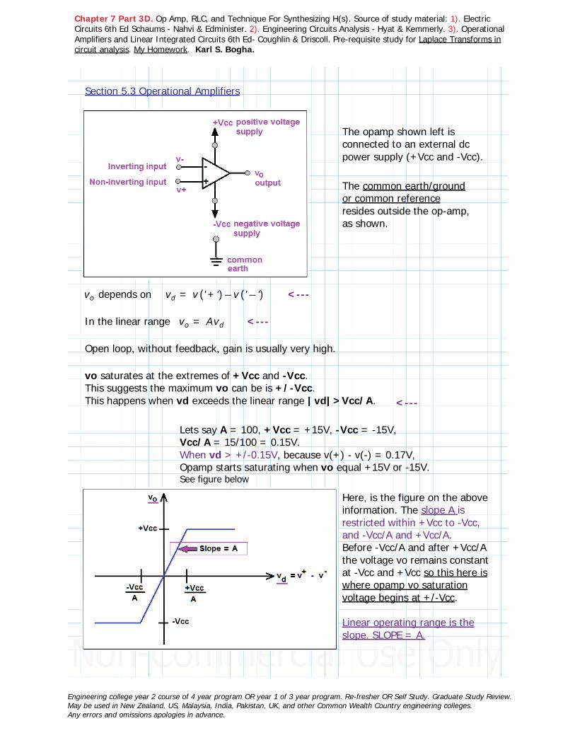
Section 5.3 Operational Amplifiers
The opamp shown left is connected to an external dc power supply (+Vcc and -Vcc).
The common earth/ground or common referenceresides outside the op-amp, as shown.
vo depends on vd = −v (( +' ')) v (( −' ')) <---
In the linear range vo = Avd <---
Open loop, without feedback, gain is usually very high.
vo saturates at the extremes of +Vcc and -Vcc. This suggests the maximum vo can be is +/-Vcc.This happens when vd exceeds the linear range |vd|>Vcc/A. <---
Lets say A = 100, +Vcc = +15V, -Vcc = -15V,Vcc/A = 15/100 = 0.15V.When vd > +/-0.15V, because v(+) - v(-) = 0.17V,Opamp starts saturating when vo equal +15V or -15V. See figure below
Here, is the figure on the above information. The slope A is restricted within +Vcc to -Vcc, and -Vcc/A and +Vcc/A.Before -Vcc/A and after +Vcc/A the voltage vo remains constant at -Vcc and +Vcc so this here is where opamp vo saturation voltage begins at +/-Vcc.
Linear operating range is the slope. SLOPE = A.
Engineering college year 2 course of 4 year program OR year 1 of 3 year program. Re-fresher OR Self Study. Graduate Study Review.May be used in New Zealand, US, Malaysia, India, Pakistan, UK, and other Common Wealth Country engineering colleges.Any errors and omissions apologies in advance.

Chapter 7 Part 3D. Op Amp, RLC, and Technique For Synthesizing H(s). Source of study material: 1). Electric Circuits 6th Ed Schaums - Nahvi & Edminister. 2). Engineering Circuits Analysis - Hyat & Kemmerly. 3). Operational Amplifiers and Linear Integrated Circuits 6th Ed- Coughlin & Driscoll. Pre-requisite study for Laplace Transforms in circuit analysis. My Homework. Karl S. Bogha.
This figure is a simple model of the opamp, without the dc supply voltage, +Vcc/-Vcc, in the linear range.
Linear range is where vo = Avd = A ( v(+) - v(-) ).
Ri is large, Ro is small, and A varies from 10^5 to several millions.The model is valid so long as vo, output, remains between +Vcc and -Vcc.Vcc is generally 5 - 18V.- With Ri very large the current entering v(-) the inverting input terminal will be very low, in ideal condition zero. - Ro is small, so the current flow out of the opamp is not impeded it may be as high as possible.
Example 5:
Vcc = 15V, A = 10^5, and v(-) = 0.Find the upper limit on the magnitude of v(+) for linear operation ?
Solution:Vcc terminal was not shown just to make it simple. Shown above.
≔Vcc 15 ≔A 105 ≔vminus 0
vo = A vd = A (v+ - v-) = Av+ - Av- = Av+ - A(0) = Av+ - 0 = Av+
vo = A v+ = ⋅⎛⎝105 ⎞⎠ vplus
Engineering college year 2 course of 4 year program OR year 1 of 3 year program. Re-fresher OR Self Study. Graduate Study Review.May be used in New Zealand, US, Malaysia, India, Pakistan, UK, and other Common Wealth Country engineering colleges.Any errors and omissions apologies in advance.

Chapter 7 Part 3D. Op Amp, RLC, and Technique For Synthesizing H(s). Source of study material: 1). Electric Circuits 6th Ed Schaums - Nahvi & Edminister. 2). Engineering Circuits Analysis - Hyat & Kemmerly. 3). Operational Amplifiers and Linear Integrated Circuits 6th Ed- Coughlin & Driscoll. Pre-requisite study for Laplace Transforms in circuit analysis. My Homework. Karl S. Bogha.
v(+)<--- must not be greater than +/-Vcc which here is less
than or equal 15V. So upper limit is 15V.
The linear operating range is the slope.
vo = A v+ = ⋅⎛⎝105 ⎞⎠ vplus
vplus is v(+)
≔vo_UpLimit 15
vo = A v+ = vo_UpperLimit
v+ = vo_UpperLimit / A
≔vplus =――――vo_UpLimit
A0.0002 = ⋅150 10−6
|v(+)| = 150 microvolt Answer.
Comments:
What the answer is saying is v- = 0 and v+ = 150uV.Which is saying vd = 150uv - 0V = 150uV.That is such a low voltage at the input terminals of the opamp.Electronics? NOT power system not transmission line voltage in kV.OK so its low. What else? Found out how to set the upper limit for the input signal, when given the A and v(-) = 0, and the opamp dc voltage supply here was 15V.
In other words in that linear range the voltage is a slope and outside it its no higher or lower then +Vcc and -Vcc.
Engineering college year 2 course of 4 year program OR year 1 of 3 year program. Re-fresher OR Self Study. Graduate Study Review.May be used in New Zealand, US, Malaysia, India, Pakistan, UK, and other Common Wealth Country engineering colleges.Any errors and omissions apologies in advance.

Chapter 7 Part 3D. Op Amp, RLC, and Technique For Synthesizing H(s). Source of study material: 1). Electric Circuits 6th Ed Schaums - Nahvi & Edminister. 2). Engineering Circuits Analysis - Hyat & Kemmerly. 3). Operational Amplifiers and Linear Integrated Circuits 6th Ed- Coughlin & Driscoll. Pre-requisite study for Laplace Transforms in circuit analysis. My Homework. Karl S. Bogha.
Example 6:
Given Vcc = 5V, A = 10^5, v(-) = 0 and v(+) = 100 sin 2 pi t (uV).
Find and sketch the open loop output vo?
Solution:What is the opamp input voltage?
vd = v(+) - v(-)
vd = 100 sin (2 pi) t - 0
≔vd ((t)) ⋅⋅100 sin (( ⋅⋅2 π t)) 10−6 V
Comment: That troubled me a little, the signal enters v(-) inverting, and on the Ro side in the diamond shape +ve is on top. Avd its a positive value for vd.
Input signal shown below, amplitude 100, w = 2pi so one cycle in 1 second.
-6⋅10⁻⁵-4⋅10⁻⁵-2⋅10⁻⁵
02⋅10⁻⁵4⋅10⁻⁵6⋅10⁻⁵8⋅10⁻⁵
-0.0001-8⋅10⁻⁵
0.0001
0.2 0.3 0.4 0.5 0.6 0.7 0.8 0.90 0.1 1
t
vd ((t))
I know the peak cannot go pass 5V (Vcc) for the linear operating range (slope).
Engineering college year 2 course of 4 year program OR year 1 of 3 year program. Re-fresher OR Self Study. Graduate Study Review.May be used in New Zealand, US, Malaysia, India, Pakistan, UK, and other Common Wealth Country engineering colleges.Any errors and omissions apologies in advance.

Chapter 7 Part 3D. Op Amp, RLC, and Technique For Synthesizing H(s). Source of study material: 1). Electric Circuits 6th Ed Schaums - Nahvi & Edminister. 2). Engineering Circuits Analysis - Hyat & Kemmerly. 3). Operational Amplifiers and Linear Integrated Circuits 6th Ed- Coughlin & Driscoll. Pre-requisite study for Laplace Transforms in circuit analysis. My Homework. Karl S. Bogha.
Input signal is uV (10^-6).Opamp multiplier is 10^5, this makes the signal vo:
≔A 105
vo = A v_d
vo = ⋅⋅⋅100 sin (( ⋅⋅2 π t)) 10−6 105
≔vo ((t)) ⋅10 sin (( ⋅⋅2 π t)) Answer.
I need to cut-off the peak at +5V and -5V.
To make it a simple plot I will draw a horizontal line in at +5 and -5.
-3-2-1
01234
-5-4
5
0 0.5 1
5
−5
0.083 0.417
t
vo ((t))
vo behaviour as shown below:
Answer.
The input voltage is clipped off at +/-5V. Opamp saturation starts at when vo equal 10sin(2 PI t) reaches +/- 5V.Opamp is operating within +5 and -5V.The time intervals for the +5V and -5V are provided below.
<--- +5Vvo ---> <--- - 5V
Answer.<--- 10sin( 2Pi t)V
=―1
120.0833 =―
512
0.4167 =―7
120.5833 =―
1112
0.9167
Above two positive side time t shown on plot.
Above two negative side time t not shown on plot.
Engineering college year 2 course of 4 year program OR year 1 of 3 year program. Re-fresher OR Self Study. Graduate Study Review.May be used in New Zealand, US, Malaysia, India, Pakistan, UK, and other Common Wealth Country engineering colleges.Any errors and omissions apologies in advance.

Chapter 7 Part 3D. Op Amp, RLC, and Technique For Synthesizing H(s). Source of study material: 1). Electric Circuits 6th Ed Schaums - Nahvi & Edminister. 2). Engineering Circuits Analysis - Hyat & Kemmerly. 3). Operational Amplifiers and Linear Integrated Circuits 6th Ed- Coughlin & Driscoll. Pre-requisite study for Laplace Transforms in circuit analysis. My Homework. Karl S. Bogha.
Example 7:
Repeat Example 6 for v(-) = 25 uV, and v(+) = 50 sin (2 PI t) uV.
≔A 105
Same as Example 6.
Solution:
Need to solve for vd first.
vminus = ⋅25 10−6 V
vplus = ⋅⋅50 sin (( ⋅⋅2 π t)) 10−6 V
−vplus vminus = −⋅⋅50 sin (( ⋅⋅2 π t)) 10−6 ⋅25 10−6 V
= ⋅(( ⋅⋅50 sin (( ⋅⋅2 π t)) −25)) 10−6 V
= ⋅⋅50 sin (( −2 πt 25)) 10−6 V25 fits in like a phase angle.
−vplus vminus = ⋅⎛⎝ ⋅50 10−6⎞⎠ sin ⎛⎜⎝−2 πt ―
12⎞⎟⎠
V The half makes 25 when multiplied by 50, and multiplied by 10^-6 keeps it all in uV.
vd ((t)) = ⋅⎛⎝ ⋅50 10−6⎞⎠ sin ⎛⎜⎝−2 πt ―
12⎞⎟⎠
V
vo = ⋅A vd ((t)) = ⋅⋅105 ⎛⎝ ⋅50 10−6⎞⎠ sin ⎛⎜⎝−2 πt ―
12⎞⎟⎠
V
vo = ⋅5 sin ⎛⎜⎝−2 πt ―
12⎞⎟⎠
V. <--- Opamp output when its within the linear range.
Engineering college year 2 course of 4 year program OR year 1 of 3 year program. Re-fresher OR Self Study. Graduate Study Review.May be used in New Zealand, US, Malaysia, India, Pakistan, UK, and other Common Wealth Country engineering colleges.Any errors and omissions apologies in advance.

Chapter 7 Part 3D. Op Amp, RLC, and Technique For Synthesizing H(s). Source of study material: 1). Electric Circuits 6th Ed Schaums - Nahvi & Edminister. 2). Engineering Circuits Analysis - Hyat & Kemmerly. 3). Operational Amplifiers and Linear Integrated Circuits 6th Ed- Coughlin & Driscoll. Pre-requisite study for Laplace Transforms in circuit analysis. My Homework. Karl S. Bogha.
clear ((t))
vo = ⋅5 sin ⎛⎜⎝−2 πt ―
12⎞⎟⎠
= −⋅5 sin (( ⋅⋅2 π t)) 2.5 Answer.
≔vo ((t)) −⋅5 sin (( ⋅⋅2 π t)) 2.5
-6
-5-4
-3-2
-10
12
345
67
-8
-7
8
0 0.25 0.5 0.75 1-0.5 -0.25 1.25
5
−5
0.583 0.917
t
vo ((t))
Answer.=―
712
0.5833 =―1112
0.9167 <--- two negative side time t shown on plot.
Same as before the saturation voltage is +/-5V.The output signal's waveform must be flat at +/-5V.
The positive side, above 0, waveform does not cross 5V.The bottom, negative side crosses -5V this side of the waveform need to be made flat when it goes past -5V.
<--- 5 sin ( 2 Pi t - 1/2) Vvo --->
<--- - 5V Answer.
Engineering college year 2 course of 4 year program OR year 1 of 3 year program. Re-fresher OR Self Study. Graduate Study Review.May be used in New Zealand, US, Malaysia, India, Pakistan, UK, and other Common Wealth Country engineering colleges.Any errors and omissions apologies in advance.
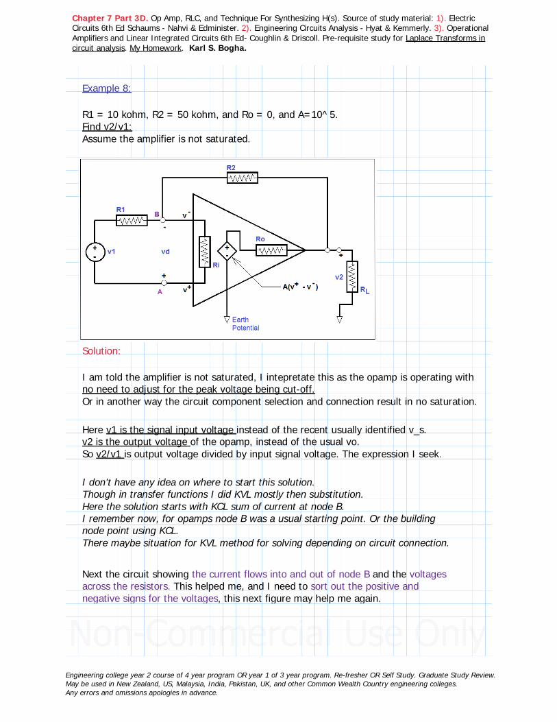
Chapter 7 Part 3D. Op Amp, RLC, and Technique For Synthesizing H(s). Source of study material: 1). Electric Circuits 6th Ed Schaums - Nahvi & Edminister. 2). Engineering Circuits Analysis - Hyat & Kemmerly. 3). Operational Amplifiers and Linear Integrated Circuits 6th Ed- Coughlin & Driscoll. Pre-requisite study for Laplace Transforms in circuit analysis. My Homework. Karl S. Bogha.
Example 8:
R1 = 10 kohm, R2 = 50 kohm, and Ro = 0, and A=10^5.Find v2/v1:Assume the amplifier is not saturated.
Solution:
I am told the amplifier is not saturated, I intepretate this as the opamp is operating with no need to adjust for the peak voltage being cut-off.Or in another way the circuit component selection and connection result in no saturation.
Here v1 is the signal input voltage instead of the recent usually identified v_s.v2 is the output voltage of the opamp, instead of the usual vo.So v2/v1 is output voltage divided by input signal voltage. The expression I seek.
I don't have any idea on where to start this solution.Though in transfer functions I did KVL mostly then substitution.Here the solution starts with KCL sum of current at node B.I remember now, for opamps node B was a usual starting point. Or the building node point using KCL. There maybe situation for KVL method for solving depending on circuit connection.
Next the circuit showing the current flows into and out of node B and the voltages across the resistors. This helped me, and I need to sort out the positive and negative signs for the voltages, this next figure may help me again.
Engineering college year 2 course of 4 year program OR year 1 of 3 year program. Re-fresher OR Self Study. Graduate Study Review.May be used in New Zealand, US, Malaysia, India, Pakistan, UK, and other Common Wealth Country engineering colleges.Any errors and omissions apologies in advance.

Chapter 7 Part 3D. Op Amp, RLC, and Technique For Synthesizing H(s). Source of study material: 1). Electric Circuits 6th Ed Schaums - Nahvi & Edminister. 2). Engineering Circuits Analysis - Hyat & Kemmerly. 3). Operational Amplifiers and Linear Integrated Circuits 6th Ed- Coughlin & Driscoll. Pre-requisite study for Laplace Transforms in circuit analysis. My Homework. Karl S. Bogha.
Figure with current flows and voltages identified at node B and output.
vd = v(+) - v(-) how I seen recently so why need to change ?It gives the voltage at node B. Whatever v(-) value is if it were higher than v(+), its still vd the voltage difference across the input resistor Ri. Because the current entering the node 2 is so small practically zero with a high resistance Ri that gives it some appreciable voltage rise; i_entering -ve terminal is aprox zero multiply it by Ri results in some voltage that is? vd. WRONG! Lets try again. The first figure with internal of the opamp? Terminal 7 and 4. Opamp input voltage +Vcc and -Vcc.
The figure to the left has positive power supply coming in at terminal 7, that is +Vcc. At terminal 4 thats negative power suppy coming in that is -Vcc.
The arrow for current I causes a voltage inside the opamp circuitry, which is shown as v1 here.
This voltage v1 is vd, differential input voltage between terminal 2 and 3.Inside the opamp.
Otherwise its same as v_s input signal voltage and if relevant subtract vR1 should there be a resistor R1 like in this example.
Engineering college year 2 course of 4 year program OR year 1 of 3 year program. Re-fresher OR Self Study. Graduate Study Review.May be used in New Zealand, US, Malaysia, India, Pakistan, UK, and other Common Wealth Country engineering colleges.Any errors and omissions apologies in advance.

Chapter 7 Part 3D. Op Amp, RLC, and Technique For Synthesizing H(s). Source of study material: 1). Electric Circuits 6th Ed Schaums - Nahvi & Edminister. 2). Engineering Circuits Analysis - Hyat & Kemmerly. 3). Operational Amplifiers and Linear Integrated Circuits 6th Ed- Coughlin & Driscoll. Pre-requisite study for Laplace Transforms in circuit analysis. My Homework. Karl S. Bogha.
Voltage at node A is reference or earth potential at 0V.
Voltage at node B is vd, since its a negative polarity at the non-inverting input terminal 2 this is now -vd.
vA = 0 V
vB = −vd V. The exact value can be determined from data sheets of specific manufacturer.
IR1 = ――――−v1 ((−vd))
R1= ―――
+v1 vd10 k
IR2 = ――――−v2 ((−vd))
R2= ―――
+v2 vd50 k
IRi = ――――−0 ((−vd))
R2= ――
vd500 k
<---- Correct here vd's voltage is measured from point B to A, which is relative to 0V at A, therefore the voltage is positive vd. Its just the way its written and makes the intended choice. Otherwise if its written (-vd) - 0 this would be -vd ! Call it Logic or Convention seems they need to be united not opposing - Karl Bogha.
Sum of currents at node B :
++⎛⎜⎝―――
+v1 vd10 k
⎞⎟⎠⎛⎜⎝―――
+v2 vd50 k
⎞⎟⎠⎛⎜⎝――
vd500 k
⎞⎟⎠
= 0 Can cancel out the k (1000) in all the denominators as its common.
++⎛⎜⎝―――
+v1 vd10
⎞⎟⎠⎛⎜⎝―――
+v2 vd50
⎞⎟⎠⎛⎜⎝――vd
500⎞⎟⎠
= 0
Going back to the transfer function method to solve, I need to represent one variable for another so I may attain my function.
Engineering college year 2 course of 4 year program OR year 1 of 3 year program. Re-fresher OR Self Study. Graduate Study Review.May be used in New Zealand, US, Malaysia, India, Pakistan, UK, and other Common Wealth Country engineering colleges.Any errors and omissions apologies in advance.

Chapter 7 Part 3D. Op Amp, RLC, and Technique For Synthesizing H(s). Source of study material: 1). Electric Circuits 6th Ed Schaums - Nahvi & Edminister. 2). Engineering Circuits Analysis - Hyat & Kemmerly. 3). Operational Amplifiers and Linear Integrated Circuits 6th Ed- Coughlin & Driscoll. Pre-requisite study for Laplace Transforms in circuit analysis. My Homework. Karl S. Bogha.
How do I do that?
vo = A x vd
v2 = vo.
This will make v2 disappear from the expression leaving v1 and vd.ORHave vd represented in v2 and have vd disappear. This is what I need, leaving v1 and v2.
v2 = 105 vd
vd = ――v2
105= ⋅v2 10−5
++⎛⎜⎝―――
+v1 vd10
⎞⎟⎠⎛⎜⎝―――
+v2 vd50
⎞⎟⎠⎛⎜⎝――vd
500⎞⎟⎠
= 0
++⎛⎜⎝―――――
+v1 ⋅v2 10−5
10
⎞⎟⎠
⎛⎜⎝―――――
+v2 ⋅v2 10−5
50
⎞⎟⎠
⎛⎜⎝―――⋅v2 10−5
500
⎞⎟⎠
= 0
――――――――――――――――++⋅50 ⎛⎝ +v1 ⋅v2 10−5⎞⎠ ⋅10 ⎛⎝ +v2 ⋅v2 10−5⎞⎠ ⎛⎝ ⋅v2 10−5⎞⎠
500= 0
――――――――――――――――++++⋅50 v1 ⋅50 v2 10−5 ⋅10 v2 ⋅10 v2 10−5 ⋅v2 10−5
500= 0
―――――――――++⋅50 v1 ⋅61 v2 10−5 ⋅10 v2
500= 0
―――――――――++⋅50 v1 ⋅0.00061 v2 10 v2
500= 0 Multiply by 500
+50 v1 10.00061 v2 = 0 10.00061 v2 approximately equal 10 v2
+50 v1 10 v2 = 0
10 v2 = −50 v1
―v2v1
= −―5010
= −5 Answer.
Engineering college year 2 course of 4 year program OR year 1 of 3 year program. Re-fresher OR Self Study. Graduate Study Review.May be used in New Zealand, US, Malaysia, India, Pakistan, UK, and other Common Wealth Country engineering colleges.Any errors and omissions apologies in advance.
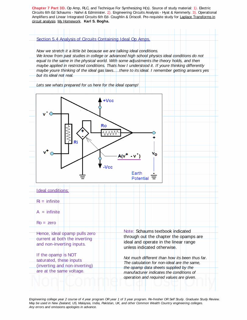
Chapter 7 Part 3D. Op Amp, RLC, and Technique For Synthesizing H(s). Source of study material: 1). Electric Circuits 6th Ed Schaums - Nahvi & Edminister. 2). Engineering Circuits Analysis - Hyat & Kemmerly. 3). Operational Amplifiers and Linear Integrated Circuits 6th Ed- Coughlin & Driscoll. Pre-requisite study for Laplace Transforms in circuit analysis. My Homework. Karl S. Bogha.
Section 5.4 Analysis of Circuits Containing Ideal Op Amps.
Now we stretch it a little bit because we are talking ideal conditions.We know from past studies in college or advanced high school physics ideal conditions do not equal to the same in the physical world. With some adjustments the theory holds, and then maybe applied in restricted conditions. Thats how I understood it. If youre thinking differently maybe youre thinking of the ideal gas laws.....there to its ideal. I remember getting answers yes but its ideal not real.
Lets see whats prepared for us here for the ideal opamp!
Ideal conditions:
Ri = infinite
A = infinite
Ro = zero
Hence, ideal opamp pulls zero current at both the inverting and non-inverting inputs.
If the opamp is NOT saturated, these inputs (inverting and non-inverting) are at the same voltage.
Note: Schaums textbook indicated through out the chapter the opamps are ideal and operate in the linear range unless indicated otherwise.
Not much different than how its been thus far. The calculation for non-ideal are the same, the opamp data sheets supplied by the manufacturer indicates the conditions of operation and required values are given.
Engineering college year 2 course of 4 year program OR year 1 of 3 year program. Re-fresher OR Self Study. Graduate Study Review.May be used in New Zealand, US, Malaysia, India, Pakistan, UK, and other Common Wealth Country engineering colleges.Any errors and omissions apologies in advance.

Chapter 7 Part 3D. Op Amp, RLC, and Technique For Synthesizing H(s). Source of study material: 1). Electric Circuits 6th Ed Schaums - Nahvi & Edminister. 2). Engineering Circuits Analysis - Hyat & Kemmerly. 3). Operational Amplifiers and Linear Integrated Circuits 6th Ed- Coughlin & Driscoll. Pre-requisite study for Laplace Transforms in circuit analysis. My Homework. Karl S. Bogha.
Example 5.9 (Circuit on opamp model internals thru external connections):
The op-amp circuit shown below is ideal and not saturated.
Find a). v2/v1
b). input resistance v1 / i1
c). i1, i2, and p1 (power delivered by v1)
d). p2 (power dissipated in the resistors)
Given v1 = 0.5V
Ideal conditions:
Ri = infinite
A = infinite
Ro = zero
Hence, ideal opamp pulls zero current at the inverting input and zero current exiting at non-inverting input.
If the opamp is NOT saturated, these inputs (inverting and non-inverting) are at the same voltage.
Solution:
Lets begin by setting the voltages in the circuit:
vA = 0 V its connected to earth reference 0V.vB = 0 V because Ri is infinite so no current can flow thru the -ve terminal. vB is at same earth potential as vA.
Apply KCL, sum of currents, at nodes B and C.
With the understanding here, ideal conditions, that with A tied to 0V ref, the opamp is not pulling in (drawing) any current.
Continued next page.
Engineering college year 2 course of 4 year program OR year 1 of 3 year program. Re-fresher OR Self Study. Graduate Study Review.May be used in New Zealand, US, Malaysia, India, Pakistan, UK, and other Common Wealth Country engineering colleges.Any errors and omissions apologies in advance.

Chapter 7 Part 3D. Op Amp, RLC, and Technique For Synthesizing H(s). Source of study material: 1). Electric Circuits 6th Ed Schaums - Nahvi & Edminister. 2). Engineering Circuits Analysis - Hyat & Kemmerly. 3). Operational Amplifiers and Linear Integrated Circuits 6th Ed- Coughlin & Driscoll. Pre-requisite study for Laplace Transforms in circuit analysis. My Homework. Karl S. Bogha.
Circuit connection with voltages identified at nodes and current flows.
Since all the resistors are in kilo ohms I can drop the 10^3 in the calculation.
Sum of currents at node B (KCL) :
Break-off and Return (Detour): The 5kohm resistor has one side of terminal connected to v1, the other side is NOT connected to node B. Rather before node B, and at this end of the 5 kohm resistor the voltage drop is IR (I x 5kohm). This voltage drop is v1. Why is it the same as the input voltage source? Because the voltage at node B is 0V, hence, v1 has to end at end of 5 kohm resistor, but current continues to flow to 10 kohm resistor by-passing the -ve terminal of opamp as the resistance here is infinite. Some explanation given in circuit figure above. Its confusing enough for me and its just the start of circuits! Prior exercises I did not encounter the exact situation. I hope it helped you as much as it did me. You may wind-up taking a law degree after your engineering degree this because of the justification you had to provide in circuits helped build your lawyering intuition - Karl Bogha.
++――−0 v15
―――−0 vC10
―――0
Infinite= 0
−−―v15――vC10
= 0
Engineering college year 2 course of 4 year program OR year 1 of 3 year program. Re-fresher OR Self Study. Graduate Study Review.May be used in New Zealand, US, Malaysia, India, Pakistan, UK, and other Common Wealth Country engineering colleges.Any errors and omissions apologies in advance.

Chapter 7 Part 3D. Op Amp, RLC, and Technique For Synthesizing H(s). Source of study material: 1). Electric Circuits 6th Ed Schaums - Nahvi & Edminister. 2). Engineering Circuits Analysis - Hyat & Kemmerly. 3). Operational Amplifiers and Linear Integrated Circuits 6th Ed- Coughlin & Driscoll. Pre-requisite study for Laplace Transforms in circuit analysis. My Homework. Karl S. Bogha.
――vC10
= −―v15
vC = ―――−v1 ((10))
5= −2 v1
Sum of currents at node C :
++―――−vC 0
10―――−vC 0
1―――−vC v22
= 0 ---> ++――vC10
――vC1
―――−vC v22
= 0
――――――――−++vC 10 vC 5 vC 5 v2
10= 0
―――――−16 vC 5 v2
10= 0
−1.6 vC 0.5 v2 = 0
0.5 v2 = 1.6 vC
v2 = ――1.60.5
vC = ――1.6⎛⎜⎝―12⎞⎟⎠
vC = 3.2 vC
v2 = 3.2 vC
vC = ――v23.2
Substitute OR exchange vC in this expression we got already --> vC = −2 v1
――v23.2
= −2 v1
―v2v1
= −6.4 Answer.
Next for the input resistance.This is the resistance of the opamp at its input terminal.See figure to the right Ri.Voltage across Ri is vB.
vRi = vB = 0
Engineering college year 2 course of 4 year program OR year 1 of 3 year program. Re-fresher OR Self Study. Graduate Study Review.May be used in New Zealand, US, Malaysia, India, Pakistan, UK, and other Common Wealth Country engineering colleges.Any errors and omissions apologies in advance.
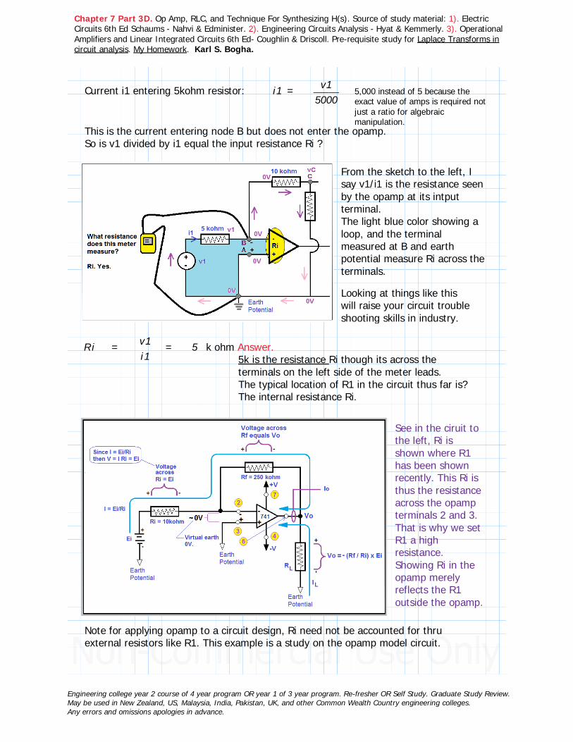
Chapter 7 Part 3D. Op Amp, RLC, and Technique For Synthesizing H(s). Source of study material: 1). Electric Circuits 6th Ed Schaums - Nahvi & Edminister. 2). Engineering Circuits Analysis - Hyat & Kemmerly. 3). Operational Amplifiers and Linear Integrated Circuits 6th Ed- Coughlin & Driscoll. Pre-requisite study for Laplace Transforms in circuit analysis. My Homework. Karl S. Bogha.
Current i1 entering 5kohm resistor: i1 = ――v1
50005,000 instead of 5 because the exact value of amps is required not just a ratio for algebraic manipulation.
This is the current entering node B but does not enter the opamp.So is v1 divided by i1 equal the input resistance Ri ?
From the sketch to the left, I say v1/i1 is the resistance seen by the opamp at its intput terminal.The light blue color showing a loop, and the terminal measured at B and earth potential measure Ri across the terminals.
Looking at things like this will raise your circuit trouble shooting skills in industry.
Ri = ―v1i1
= 5 k ohm Answer.5k is the resistance Ri though its across the
terminals on the left side of the meter leads. The typical location of R1 in the circuit thus far is? The internal resistance Ri.
See in the ciruit to the left, Ri is shown where R1 has been shown recently. This Ri is thus the resistance across the opamp terminals 2 and 3.That is why we set R1 a high resistance. Showing Ri in the opamp merely reflects the R1 outside the opamp.
Note for applying opamp to a circuit design, Ri need not be accounted for thru external resistors like R1. This example is a study on the opamp model circuit.
Engineering college year 2 course of 4 year program OR year 1 of 3 year program. Re-fresher OR Self Study. Graduate Study Review.May be used in New Zealand, US, Malaysia, India, Pakistan, UK, and other Common Wealth Country engineering colleges.Any errors and omissions apologies in advance.

Chapter 7 Part 3D. Op Amp, RLC, and Technique For Synthesizing H(s). Source of study material: 1). Electric Circuits 6th Ed Schaums - Nahvi & Edminister. 2). Engineering Circuits Analysis - Hyat & Kemmerly. 3). Operational Amplifiers and Linear Integrated Circuits 6th Ed- Coughlin & Driscoll. Pre-requisite study for Laplace Transforms in circuit analysis. My Homework. Karl S. Bogha.
Problem statement gives vi = 0.5V.This numerical value allows me to calculate the current i1.
≔v1 0.5 ≔R1 5000
≔i1 =――v1R1
⋅1 10−4 = ⋅0.1 10−3 = 0.1 mA Answer.
For i2, set up sum of currents at output node of op amp shown in figure below:
++i2 ⎛⎜⎝――−v2 0
8000⎞⎟⎠⎛⎜⎝―――−v2 vC
2000⎞⎟⎠
= 0
−++i2 ――v2
8000――
v22000
――vC
2000= 0
i2 = +−−――v2
8000――
v22000
――vC
2000
i2 = ――――――+−−v2 4 v2 4 vC
8000
i2 = ⎛⎜⎝――――
−4 vC 5 v28000
⎞⎟⎠
vC = −2 v1 = ⋅−2 ((0.5)) = −1 This expression from earlier part of solution.
v2 = 3.2 vC = 3.2 ((−1)) = −3.2
i2 = ⎛⎜⎝――――
−4 vC 5 v28000
⎞⎟⎠
= ⎛⎜⎝――――――
−4 ((−1)) 5 ((−3.2))8000
⎞⎟⎠
= ⎛⎜⎝―――
+−4 168000
⎞⎟⎠
= ――128000
i2 = ――12
8000= =――
128000
0.0015
i2 = 0.15 mA. Answer.
Next for the power delivered by p1:This will be power delivered by the signal voltage source v1.
p1 = ⋅v1 i1 = =⋅⋅0.5 0.1 10−3 ⋅50 10−6 = 50 uW Answer.
OR ⋅v1 i1 = =⋅v1 ⎛⎜⎝――v1R1⎞⎟⎠
⋅50 10−6 uW Answer.
Engineering college year 2 course of 4 year program OR year 1 of 3 year program. Re-fresher OR Self Study. Graduate Study Review.May be used in New Zealand, US, Malaysia, India, Pakistan, UK, and other Common Wealth Country engineering colleges.Any errors and omissions apologies in advance.

Chapter 7 Part 3D. Op Amp, RLC, and Technique For Synthesizing H(s). Source of study material: 1). Electric Circuits 6th Ed Schaums - Nahvi & Edminister. 2). Engineering Circuits Analysis - Hyat & Kemmerly. 3). Operational Amplifiers and Linear Integrated Circuits 6th Ed- Coughlin & Driscoll. Pre-requisite study for Laplace Transforms in circuit analysis. My Homework. Karl S. Bogha.
I cannot do the same for p2, ie power at the output terminal.Because I do not have the opamp's impedance or voltage the opamp is operating at its internal. However, I can add up the power of all the connected resistors to sum up for the output power p2.
p = ⋅v i = ⋅v ⎛⎜⎝―vR⎞⎟⎠
= ―v2
R
p_1_kohm = ―――vC2
1 kohm= =―――
((−1))2
10000.001 W = 1000 uW Ans.
p_2_kohm = ――――(( −vC v2))
2
2 kohm= =―――――
(( −−1 ((−3.2))))2
20000.00242 W = 2420 uW Ans.
p_5_kohm = ――――(( −v1 vB))
2
5 kohm= =――――
(( −0.5 0))2
50000.00005 W = 50 uW Ans.
p_8_kohm = ―――(( −v2 0))
2
8 kohm= =―――
((−3.2))2
80000.00128 W = 1280 uW Ans.
p_10_kohm= ――――(( −vC vB))
2
10 kohm= =――――
(( −−1 0))2
100000.0001 W = 100 uW Ans.
All the above resistors are connected to the opamp.Their sum will result in the total power dissipiated by all resistors.This sum will equal p2.
≔p2 =++++1000 2420 50 1280 100 4850 uW
p2 = 4850 uW Answer.
Comments:
This example makes good for me for my building opamp circuit skills.
Engineering college year 2 course of 4 year program OR year 1 of 3 year program. Re-fresher OR Self Study. Graduate Study Review.May be used in New Zealand, US, Malaysia, India, Pakistan, UK, and other Common Wealth Country engineering colleges.Any errors and omissions apologies in advance.

Chapter 7 Part 3D. Op Amp, RLC, and Technique For Synthesizing H(s). Source of study material: 1). Electric Circuits 6th Ed Schaums - Nahvi & Edminister. 2). Engineering Circuits Analysis - Hyat & Kemmerly. 3). Operational Amplifiers and Linear Integrated Circuits 6th Ed- Coughlin & Driscoll. Pre-requisite study for Laplace Transforms in circuit analysis. My Homework. Karl S. Bogha.
Section 5.5 Inverting Circuit :
The input signal v1 is connected thru the resistor R1 to the negative terminal of the opamp, (B) shown in figure to left.
The output terminal is connected thru the feedback resistor R2, to the inverting terminal B.
The non-inverting terminal A is connected to earth potential (0V Ref).
The gain of the opamp is v2 / v1.Apply sum of currents, KCL, at node B:
+―――−vB v1
R1―――−vB v2
R2= 0
vB = 0 This I know from previous opamp section.
−−――v1R1
――v2R2
= 0
――v1R1
= −――v2R2
Gain ―v2v1
= −――R2R1
The gain is negative.Gain depends on the value of resistors R1 and R2.R1 is the input resitor. R2 the feedback resistor.
Previous circuits, pages back, for 741 --->op amp the Ri was input resistance and Rf feedback resistor.
Ri is R1 and Rf is R2 for this Section 5.5.
Ri here meaning the input not internal.
Engineering college year 2 course of 4 year program OR year 1 of 3 year program. Re-fresher OR Self Study. Graduate Study Review.May be used in New Zealand, US, Malaysia, India, Pakistan, UK, and other Common Wealth Country engineering colleges.Any errors and omissions apologies in advance.
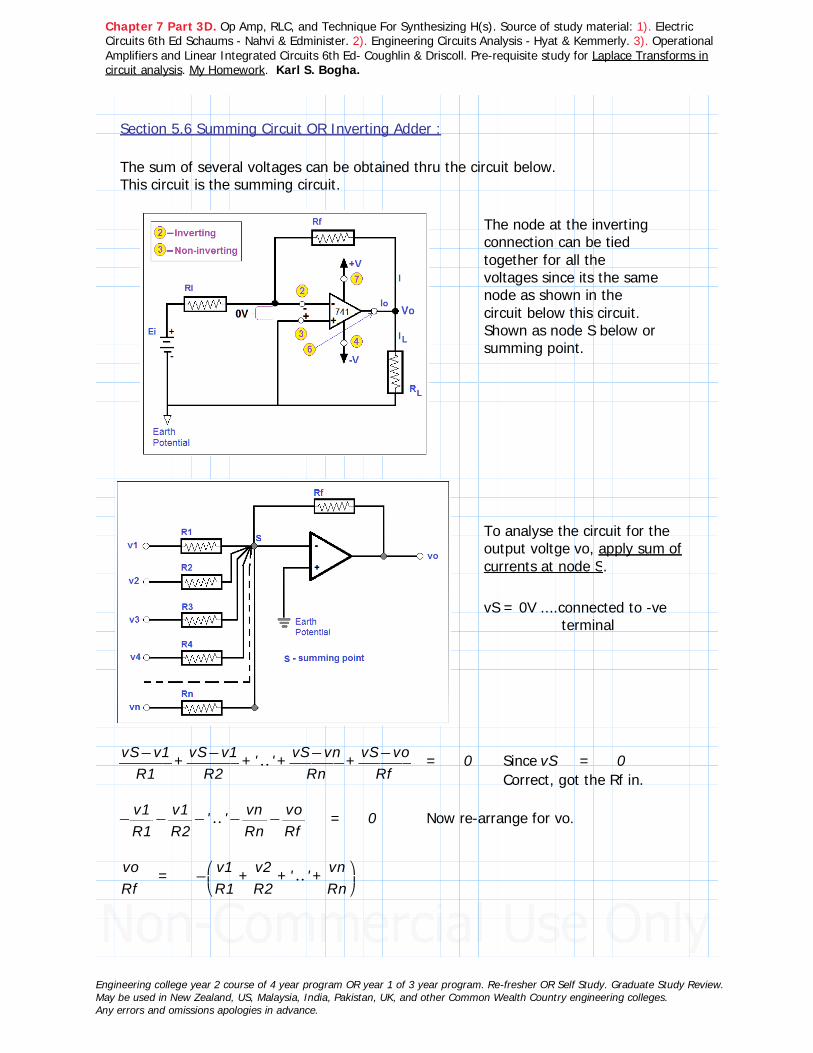
Chapter 7 Part 3D. Op Amp, RLC, and Technique For Synthesizing H(s). Source of study material: 1). Electric Circuits 6th Ed Schaums - Nahvi & Edminister. 2). Engineering Circuits Analysis - Hyat & Kemmerly. 3). Operational Amplifiers and Linear Integrated Circuits 6th Ed- Coughlin & Driscoll. Pre-requisite study for Laplace Transforms in circuit analysis. My Homework. Karl S. Bogha.
Section 5.6 Summing Circuit OR Inverting Adder :
The sum of several voltages can be obtained thru the circuit below.This circuit is the summing circuit.
The node at the inverting connection can be tied together for all the voltages since its the same node as shown in the circuit below this circuit.Shown as node S below or summing point.
To analyse the circuit for the output voltge vo, apply sum of currents at node S.
vS = 0V ....connected to -ve terminal
‥++―――−vS v1
R1―――−vS v1
R2' ++' ―――
−vS vnRn
―――−vS vo
Rf= 0 Since vS = 0
Correct, got the Rf in.
‥−−−――v1R1
――v1R2
' −−' ――vnRn
――voRf
= 0 Now re-arrange for vo.
――voRf
= −⎛⎜⎝‥++――
v1R1
――v2R2
' +' ――vnRn⎞⎟⎠
Engineering college year 2 course of 4 year program OR year 1 of 3 year program. Re-fresher OR Self Study. Graduate Study Review.May be used in New Zealand, US, Malaysia, India, Pakistan, UK, and other Common Wealth Country engineering colleges.Any errors and omissions apologies in advance.

Chapter 7 Part 3D. Op Amp, RLC, and Technique For Synthesizing H(s). Source of study material: 1). Electric Circuits 6th Ed Schaums - Nahvi & Edminister. 2). Engineering Circuits Analysis - Hyat & Kemmerly. 3). Operational Amplifiers and Linear Integrated Circuits 6th Ed- Coughlin & Driscoll. Pre-requisite study for Laplace Transforms in circuit analysis. My Homework. Karl S. Bogha.
vo = ⋅−Rf ⎛⎜⎝‥++――
v1R1
――v2R2
' +' ――vnRn⎞⎟⎠
Expanding the multiplication:
vo = −⎛⎜⎝‥++―――
⋅v1 RfR1
―――⋅v2 Rf
R2' +' ―――
⋅vn RfRn
⎞⎟⎠
In the case when R1, R2....Rn, each resistor, is of equal resistance to Rf ?R1 = R2 = ... = Rn = Rf.
Then vo = −(( ‥++v1 v2 ' +' vn)) vo equal the negative the sum of all voltages.
Example 5.10 :
Let the circuit in the figure below have four input lines.
Where R1 = 1, R2 = 1/2, R3 = 1/4, R4 = 1/8, andRf = 1.
All values in k ohm.The input lines are set to either 0V or 1V.
Find vo in terms of v4, v3, v2, and v1, given the following sets of inputs:
a). v4 = 1V, v3 = 0V, v2 = 0V, and v1 = 1V. Engineers placed v4 first, Why? come come to it later in solution.b). v4 = 1V, v3 = 1V, v2 = 1V, and v1 = 0V.
Engineering college year 2 course of 4 year program OR year 1 of 3 year program. Re-fresher OR Self Study. Graduate Study Review.May be used in New Zealand, US, Malaysia, India, Pakistan, UK, and other Common Wealth Country engineering colleges.Any errors and omissions apologies in advance.

Chapter 7 Part 3D. Op Amp, RLC, and Technique For Synthesizing H(s). Source of study material: 1). Electric Circuits 6th Ed Schaums - Nahvi & Edminister. 2). Engineering Circuits Analysis - Hyat & Kemmerly. 3). Operational Amplifiers and Linear Integrated Circuits 6th Ed- Coughlin & Driscoll. Pre-requisite study for Laplace Transforms in circuit analysis. My Homework. Karl S. Bogha.
Solution:vo = −⎛⎜⎝
+++―――⋅v1 Rf
R1―――⋅v2 Rf
R2―――⋅v3 Rf
R3―――⋅v4 Rf
R4⎞⎟⎠
= −⎛⎜⎜⎝
+++――⋅v1 1
1――⋅v2 1
―12
――⋅v3 1
―14
――⋅v4 1
―18
⎞⎟⎟⎠
In this case using the fraction form is easier instead of decimal 0.5,...,0.125.
vo = −(( +++v1 2 v2 4 v3 8 v4)) Answer.vo = −(( +++8 v4 ⋅4 v3 ⋅2 v2 v1)) Order has to be reversed; based on binary
position, v4-2^3, v3-2^2, v2-2^1, v1-2^0.At this point in the solution the engineers want to tell us this circuit can be used for a digital to analog converter.Digital values usually take on a binary form, 0 or 1. Or ON or OFF.
Here the input is a voltage value of 1V or 0V. In the first case (a), we have:v4 = 1V, v3 = 0V, v2 = 0V, and v1 = 1V. 1 0 0 1 ---> 9 for analog.case b), we have:v4 = 1V, v3 = 1V, v2 = 1V, and v1 = 0V. 1 1 1 0 ---> 14 for analog.
Arranged from highest order 2^3, 2^2, 2^1, and 2^0. 8 4 2 1 Since we have 2^3 the highest thats 8, and eight 0s and eight 1s make 16.Analog numbers for 2^3, 0 or 1, results in 0 thru 15.
<---Digital and corresponding analog values shown on table to the left.
Next plug in the values for voltages for a). and b).
a). v4 = 1V, v3 = 0V, v2 = 0V, and v1 = 1V.vo = −(( +++8 v4 ⋅4 v3 ⋅2 v2 1 v1))
= −(( +++⋅8 1 4 0 ⋅2 0 ⋅1 1))= −(( +++8 0 0 1))= −9 V Answer. Negative 9 volts is the output.
b). v4 = 1V, v3 = 1V, v2 = 1V, and v1 = 0V.vo = −(( +++8 v4 ⋅4 v3 ⋅2 v2 1 v1))
= −(( +++⋅8 1 4 1 ⋅2 1 ⋅1 0))= −(( +++8 4 2 0))= −14 Answer. Negative 14 volts is the output.
Engineering college year 2 course of 4 year program OR year 1 of 3 year program. Re-fresher OR Self Study. Graduate Study Review.May be used in New Zealand, US, Malaysia, India, Pakistan, UK, and other Common Wealth Country engineering colleges.Any errors and omissions apologies in advance.

Chapter 7 Part 3D. Op Amp, RLC, and Technique For Synthesizing H(s). Source of study material: 1). Electric Circuits 6th Ed Schaums - Nahvi & Edminister. 2). Engineering Circuits Analysis - Hyat & Kemmerly. 3). Operational Amplifiers and Linear Integrated Circuits 6th Ed- Coughlin & Driscoll. Pre-requisite study for Laplace Transforms in circuit analysis. My Homework. Karl S. Bogha.
Comments:
I could have started the solution with v4 then not having to reverse, as the engineers did. That would not allow for the natural mistake for neglecting it.Would have been as I see it straight thru v1-v4, why?...this is not a digital logic class.
vo = −⎛⎜⎝+++―――
⋅v4 RfR4
―――⋅v3 Rf
R3―――⋅v2 Rf
R2―――⋅v1 Rf
R1⎞⎟⎠
= −⎛⎜⎜⎝
+++――⋅v4 1
―18
――⋅v3 1
―14
――⋅v2 1
―12
――⋅v1 1
1⎞⎟⎟⎠
vo = −(( +++8 v4 ⋅4 v3 ⋅2 v2 v1)) Answer.Don't need to reverse anything.
Example 3-8 From C&D :
In the circuit above, E1 = 2V, E2 = 3V, and E3 = 1V,and all resistors are 10 kohm.Calculate vo ?
Solution:Note: The circuit is inverting opamp so the output vo will be -ve. As it is here -6V. I told myself will be good if I get ahead of the game and have some expectation of the circuit results. You know like an electrical engineer!
≔E1 2 ≔E2 3 ≔E3 1
vo = =−(( ++E1 E2 E3)) −6 V. Answer.
Engineering college year 2 course of 4 year program OR year 1 of 3 year program. Re-fresher OR Self Study. Graduate Study Review.May be used in New Zealand, US, Malaysia, India, Pakistan, UK, and other Common Wealth Country engineering colleges.Any errors and omissions apologies in advance.

Chapter 7 Part 3D. Op Amp, RLC, and Technique For Synthesizing H(s). Source of study material: 1). Electric Circuits 6th Ed Schaums - Nahvi & Edminister. 2). Engineering Circuits Analysis - Hyat & Kemmerly. 3). Operational Amplifiers and Linear Integrated Circuits 6th Ed- Coughlin & Driscoll. Pre-requisite study for Laplace Transforms in circuit analysis. My Homework. Karl S. Bogha.
Example 3-9 From C&D :
When the polarity of E3 is reversed, and the values remain the same as previous example.Calculate vo ?
Solution:
≔E1 2 ≔E2 3 ≔E3 −1
vo = =−(( ++E1 E2 E3)) −4 V. Answer.Setting E3 = -1 solved the solution to - 4.
vo = -( 2 + 3 + (-1) ) = - 4
Before I continue with section 5.7 non-inverting circuit.There is a small but important point to make and it comes from C&D Section 3-2 Inverting Adder and Audio Mixer; same section the two examples 3-8 and 3-9 came from. Its a circuit's thing which helps understand opamps and its use in circuits.
Audio Mixer (Briefly) :
The summming or adder circuit, has currents leaving each voltage source in parallel, E1,..E3, and when these come to node S they do not combine to form one voltage, which does not happen at a node, rather currents add together at the node.
When the circuit sees these Ei voltages it sees each relative to earth reference (0V). So each current I1..I3 characterised by voltages E1...E3 flows thru the resistor Rf, to create vRf where vRf = (I1 + I2 + I3)Rf. Here the currents sum together. But again we see at vo the voltages E1 E2 and E3 appear, which are the mic signals after? Amplification.
Engineering college year 2 course of 4 year program OR year 1 of 3 year program. Re-fresher OR Self Study. Graduate Study Review.May be used in New Zealand, US, Malaysia, India, Pakistan, UK, and other Common Wealth Country engineering colleges.Any errors and omissions apologies in advance.

Chapter 7 Part 3D. Op Amp, RLC, and Technique For Synthesizing H(s). Source of study material: 1). Electric Circuits 6th Ed Schaums - Nahvi & Edminister. 2). Engineering Circuits Analysis - Hyat & Kemmerly. 3). Operational Amplifiers and Linear Integrated Circuits 6th Ed- Coughlin & Driscoll. Pre-requisite study for Laplace Transforms in circuit analysis. My Homework. Karl S. Bogha.
Each mic has same resistance R; so R1 = R2 = R3 also = Rf. Results in output vo = -(E1 + E2 +E3). <--- No current in this expression. The currents sum in vRf.At the output vo the voltages appear again as -(E1 + E2 + E3). Each microphone sends a signal with reference to 0V ref, and the circuits sees these three voltage signals at vo. Not one Ei signal's message corrupting the other. 3 mic sounds are mixed.
Current sum at Rf:VRF = ⋅(( ++I1 I2 I3)) ⎛⎝RF⎞⎠
Voltages sum at vo:V0 = −(( ++E1 E2 E3))
Each signal from the mic appears again in individual voltages E1..E3 after amplification thru the opamp. See Summer circuit when all R's = Rf.
Discussion: I am showing in my sketch to the left, 3 signals from the 3 microphones and worst case each voltage Ei has the same magnitude, frequency, and phase angle. They do magnitude wise result to 3xEi at terminal 6, ie vo. v0 = 3Ei. However, its just the same message from each mic. The stereo speaker Ohms same here mic Ohms. R1=R2=R3=Rf=R
At node S the sum of currents equal I1 + I2 +I3.The currents add at the node S to create vRf. Correct. However each current waveform is respective of each voltage waveform, its behaviour or the message/sound it carries reflect that original message/sound from the microphone. These voltages E1 E2 and E3 at the vo terminal sum together, as we seen. vo = - (E1 + E2 + E3). When R1 = R2 = R3 = Rf.
Here the Ei voltages increase thru amplification, vo = -AEi, but the message/sound remain the same at each mic in reference to a 0V earth. Eventually later at the speaker(s) we hear all the microphones message/sound.
In my circuits waveform and other circuits examples/problems we did the same thing. Unless if these voltages were dc in series at the same branch, like dc voltage batteries, we add the voltages, not same for ac voltage sources in series we have frequency and phase angle to consider.Here each mic signal as source E was in a parallel connection.
Engineering college year 2 course of 4 year program OR year 1 of 3 year program. Re-fresher OR Self Study. Graduate Study Review.May be used in New Zealand, US, Malaysia, India, Pakistan, UK, and other Common Wealth Country engineering colleges.Any errors and omissions apologies in advance.
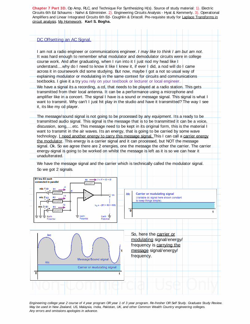
Chapter 7 Part 3D. Op Amp, RLC, and Technique For Synthesizing H(s). Source of study material: 1). Electric Circuits 6th Ed Schaums - Nahvi & Edminister. 2). Engineering Circuits Analysis - Hyat & Kemmerly. 3). Operational Amplifiers and Linear Integrated Circuits 6th Ed- Coughlin & Driscoll. Pre-requisite study for Laplace Transforms in circuit analysis. My Homework. Karl S. Bogha.
DC Offsetting an AC Signal.
I am not a radio engineer or communications engineer. I may like to think I am but am not.It was hard enough to remember what modulator and demodulator circuits were in college course work. And after graduating, when I run into it I just nod my head like I understand....why do I need to know it like I knew it, if ever I did, a nod will do I came across it in coursework did some studying. But now, maybe I got a not so usual way of explaining modulator or modulating in the same context for circuits and communications textbooks. I give it a try you rely on your textbook or lecturer or local engineer. We have a signal its a recording, a cd, that needs to be played at a radio station. This gets transmitted from their local antenna. It can be a performance using a microphone and amplifier like in a concert. The signal I have is a sound or message signal. This signal is what I want to transmit. Why can't I just hit play in the studio and have it transmitted? The way I see it, its like my cd player.
The message/sound signal is not going to be processed by any equipment. Its a ready to be transmitted audio signal. This signal is the message that is to be transmitted it can be a voice, discussion, song,....etc. This message need to be kept in its original form, this is the material I want to transmit in the air waves. Its an energy, that is going to be carried by some wave technology. I need another energy to carry this message signal. This I can call a carrier energy the modulator. This energy is a carrier signal and it can processed, but NOT the message signal. Ok. So we agree there are 2 energies, one the message the other the carrier. The carrier energy-signal is going to be worked on whilst the message is left as it is so we can hear it unadulterated.
We have the message signal and the carrier which is technically called the modulator signal. So we got 2 signals.
So, here the carrier or modulating signal/energy/frequency is carrying the message signal/energy/frequency.
Engineering college year 2 course of 4 year program OR year 1 of 3 year program. Re-fresher OR Self Study. Graduate Study Review.May be used in New Zealand, US, Malaysia, India, Pakistan, UK, and other Common Wealth Country engineering colleges.Any errors and omissions apologies in advance.

Chapter 7 Part 3D. Op Amp, RLC, and Technique For Synthesizing H(s). Source of study material: 1). Electric Circuits 6th Ed Schaums - Nahvi & Edminister. 2). Engineering Circuits Analysis - Hyat & Kemmerly. 3). Operational Amplifiers and Linear Integrated Circuits 6th Ed- Coughlin & Driscoll. Pre-requisite study for Laplace Transforms in circuit analysis. My Homework. Karl S. Bogha.
Continuing with the electric circuits on op amp. I quote the textbook paragraph with my understanding of it. Not the same situation I just described, now we have a pulsating light IRED to match the music....Some applications require that we add a dc offset voltage or current to an ac signal. Suppose that we must transmit an audio signal via an infrared emitting diode (IRED) or light emitting diode. It is first necessary to bias the IRED on with a dc current. Then the audio signal can be superimposed as an ac current that rides on or modulates the dc current. The result is a light or infrared beam whose intensity changes directly with the audio signal. Next a circuit to illustrate this principle.
In this example we are using the audio signal to play the light of the IRED to the tune of the audio signal or music. The audio signal goes to the speakers and to an IRED light.
Example 3.10 C&D :
Design a circuit that allows us to add a dc voltage to a triangle wave.
Solution:
This example presented some circuit theory that is helpful for other courses.It impressed me by its simplicity.
Make a two input adder/summing circuit. Shown in circuit below.Connect one input or channel to a dc offset voltage Edc, and the other channel or input the ac signal Eac.
Engineering college year 2 course of 4 year program OR year 1 of 3 year program. Re-fresher OR Self Study. Graduate Study Review.May be used in New Zealand, US, Malaysia, India, Pakistan, UK, and other Common Wealth Country engineering colleges.Any errors and omissions apologies in advance.

Chapter 7 Part 3D. Op Amp, RLC, and Technique For Synthesizing H(s). Source of study material: 1). Electric Circuits 6th Ed Schaums - Nahvi & Edminister. 2). Engineering Circuits Analysis - Hyat & Kemmerly. 3). Operational Amplifiers and Linear Integrated Circuits 6th Ed- Coughlin & Driscoll. Pre-requisite study for Laplace Transforms in circuit analysis. My Homework. Karl S. Bogha.
Each triangle wave input waveform Eac shown below has max at 5V and min at -5V.
Next, a few voltages for Edc.
We have a variable voltage for Edcshown in the circuit on previoius page.
Edc = 0V, -5V, and +7V.
We do purple wave for example the rest follow same. Purple plot Edc = -5V.At t = 0
v0 = - (Eac+Edc)v0 = -Eac - Edcv0 = -(-5V) - (-5V)v0 = +5V + 5Vv0 = 10V....as shown on plot.
At t = 1
v0 = - (Eac+Edc)v0 = -Eac - Edcv0 = -(5V) - (-5V)v0 = -5V + 5Vv0 = 0V....as shown on plot.
At t = 2
v0 = - (Eac+Edc)v0 = -Eac - Edcv0 = -(-5V) - (-5V)v0 = +5V + 5Vv0 = 10V....as shown on plot.
Question: Why is the Vo waveform inverted?
Answer: Because input signal connected to the inverting terminal of opamp. The input signal enters the negative terminal - inverted.
Engineering college year 2 course of 4 year program OR year 1 of 3 year program. Re-fresher OR Self Study. Graduate Study Review.May be used in New Zealand, US, Malaysia, India, Pakistan, UK, and other Common Wealth Country engineering colleges.Any errors and omissions apologies in advance.

Chapter 7 Part 3D. Op Amp, RLC, and Technique For Synthesizing H(s). Source of study material: 1). Electric Circuits 6th Ed Schaums - Nahvi & Edminister. 2). Engineering Circuits Analysis - Hyat & Kemmerly. 3). Operational Amplifiers and Linear Integrated Circuits 6th Ed- Coughlin & Driscoll. Pre-requisite study for Laplace Transforms in circuit analysis. My Homework. Karl S. Bogha.
Circuit analysis comments:
1. When Edc = 0V - brown.The brown waveform v0 is inverted compared to Eac. Correct.
At t=0, Eac = -5V, and when Edc = 0V, the output voltage v0 = -Eac - Edc = -(-5V) - 0V = 5V.
When Eac=-5V, v0=5V, which says gain A equal -1. A = -1. Eac=-5V, v0=Eac x A = -5V x -1 = 5V. In otherwords the gain A = -1.
Engineering college year 2 course of 4 year program OR year 1 of 3 year program. Re-fresher OR Self Study. Graduate Study Review.May be used in New Zealand, US, Malaysia, India, Pakistan, UK, and other Common Wealth Country engineering colleges.Any errors and omissions apologies in advance.

Chapter 7 Part 3D. Op Amp, RLC, and Technique For Synthesizing H(s). Source of study material: 1). Electric Circuits 6th Ed Schaums - Nahvi & Edminister. 2). Engineering Circuits Analysis - Hyat & Kemmerly. 3). Operational Amplifiers and Linear Integrated Circuits 6th Ed- Coughlin & Driscoll. Pre-requisite study for Laplace Transforms in circuit analysis. My Homework. Karl S. Bogha.
2. When Edc = -5V - purple.See figure to left.At t=0, Eac = -5V, and when Edc = -5V, the output voltage v0 = -Eac - Edc = -(-5V) - (-5V) = 10V.
When, Eac=-5V, v0=10V, which says gain A = v0/Eac = 10/-5 = -2. A = -2. Eac=-5V, v0 = Eac x A = -5V x -2 = 10V. In otherwords the gain A = -2?Wrong. Why?At t = 1, v0 = - (Eac+Edc); v0 = -Eac - Edcv0 = -(5V) - (-5V) = -5V + 5Vv0 = 0V....as shown on plot.v0 = A x 5V = -2 x 5 = -10V NOT Zero.So the gain is NOT -2. Correct.
Start fromtop left to top right.Then bottom left to bottom right.The thin guide lines help build the bottomright figure.
For purple waveform Vo is inverted then shifted upward by 5V. See figures above.When Edc = -5V, the output Vo appears as +5V dc offset voltage, upon which rides the inverted Eac - See above figure, bottom right, purple diagonal line. Read notes in figures.
Engineering college year 2 course of 4 year program OR year 1 of 3 year program. Re-fresher OR Self Study. Graduate Study Review.May be used in New Zealand, US, Malaysia, India, Pakistan, UK, and other Common Wealth Country engineering colleges.Any errors and omissions apologies in advance.

Chapter 7 Part 3D. Op Amp, RLC, and Technique For Synthesizing H(s). Source of study material: 1). Electric Circuits 6th Ed Schaums - Nahvi & Edminister. 2). Engineering Circuits Analysis - Hyat & Kemmerly. 3). Operational Amplifiers and Linear Integrated Circuits 6th Ed- Coughlin & Driscoll. Pre-requisite study for Laplace Transforms in circuit analysis. My Homework. Karl S. Bogha.
3. When Edc = +7V - Green
From the -5V experience, it just so happens, for the +7V the situation is similar not exact. The original signal Eac is inverted, then? shifted down 7V.Ok, -5V we shifted up and +7V we shifted down.
For the Green wave, when Edc is +7V, then Vo is shifed down 7V.The Vo Vs Eac plot is shown above.Bottom right figure horizontal axis Eac is the vertical axis Eac in top left.Same like previous figure on previous page.Question: What is the gain?Answer: See next page bottom right figure. For example when Edc =-5V, gain A = Vo/Eac. Delta y axis: Drop from 10 to 0 = -10. Negative direction slope. Delta x-axis: -5 to 5 = 10. Gain A = -10/10 = -1.
≔AEdc_minus_5 =――−1010
−1 ≔AEdc_equal_0 =――−1010
−1 ≔AEdc_7 =――−1010
−1
All the slopes have the same gain -1. Eac is transmitted with a gain of 01. Answer.
Engineering college year 2 course of 4 year program OR year 1 of 3 year program. Re-fresher OR Self Study. Graduate Study Review.May be used in New Zealand, US, Malaysia, India, Pakistan, UK, and other Common Wealth Country engineering colleges.Any errors and omissions apologies in advance.

Chapter 7 Part 3D. Op Amp, RLC, and Technique For Synthesizing H(s). Source of study material: 1). Electric Circuits 6th Ed Schaums - Nahvi & Edminister. 2). Engineering Circuits Analysis - Hyat & Kemmerly. 3). Operational Amplifiers and Linear Integrated Circuits 6th Ed- Coughlin & Driscoll. Pre-requisite study for Laplace Transforms in circuit analysis. My Homework. Karl S. Bogha.
Recap for all the waves at each Edc.
I liked this example it has a skill I can build on with regards to how to show Vo vs Eac at a specific Edc. So I gave it some extra attention. Do correct any errors and omissions. This can be used for other engineering situations as applicable. The last plot of sketch of the Vo vs Eac shows a diagonal line for each Edc, this was merely joining one end to the other of the triangle wave's maximim and minimum points.
All the slopes have a gain of -1.Read thru the figure notes any errors you can correct yourself.Next back to Schaums with Non-inverting opamp.
Engineering college year 2 course of 4 year program OR year 1 of 3 year program. Re-fresher OR Self Study. Graduate Study Review.May be used in New Zealand, US, Malaysia, India, Pakistan, UK, and other Common Wealth Country engineering colleges.Any errors and omissions apologies in advance.

Chapter 7 Part 3D. Op Amp, RLC, and Technique For Synthesizing H(s). Source of study material: 1). Electric Circuits 6th Ed Schaums - Nahvi & Edminister. 2). Engineering Circuits Analysis - Hyat & Kemmerly. 3). Operational Amplifiers and Linear Integrated Circuits 6th Ed- Coughlin & Driscoll. Pre-requisite study for Laplace Transforms in circuit analysis. My Homework. Karl S. Bogha.
Section 5.7 Non-Inverting Circuit.
Difference between inverting and non-inverting opamp is the voltage source is connected to the positive terminal.
Circuit to the left has R1 connected between -ve (inverting) terminal and earth. R2 the feedback of this circuit connected between the -ve and output terminal of the opamp.
There is enough difference here to change the gain of this simple circuit.
Find the gain v2/v1 ?
Applying sum of currents at node B.
Notice here the voltage at -ve terminal is not 0 volt rather v1 volts. Different from recent inverting opamp connection. The input resistance is again infinity and the opamp permits no appreciable current at terminal 2. 'Every electric circuit's got its own game' - Karl Bogha.
+――v1R1
―――(( −v1 v2))
R2= 0
−+――v1R1
――v1R2
――v2R2
= 0
−v1 ⎛⎜⎝+――
1R1
――1
R2⎞⎟⎠――v2R2
= 0
Engineering college year 2 course of 4 year program OR year 1 of 3 year program. Re-fresher OR Self Study. Graduate Study Review.May be used in New Zealand, US, Malaysia, India, Pakistan, UK, and other Common Wealth Country engineering colleges.Any errors and omissions apologies in advance.

Chapter 7 Part 3D. Op Amp, RLC, and Technique For Synthesizing H(s). Source of study material: 1). Electric Circuits 6th Ed Schaums - Nahvi & Edminister. 2). Engineering Circuits Analysis - Hyat & Kemmerly. 3). Operational Amplifiers and Linear Integrated Circuits 6th Ed- Coughlin & Driscoll. Pre-requisite study for Laplace Transforms in circuit analysis. My Homework. Karl S. Bogha.
v1 ⎛⎜⎝+――
1R1
――1
R2⎞⎟⎠
= ――v2R2
R2 ⎛⎜⎝+――
1R1
――1
R2⎞⎟⎠
= ―v2v1
⎛⎜⎝
+――R2R1
――R2R2⎞⎟⎠
= ―v2v1
―v2v1
= ⎛⎜⎝
+――R2R1
1⎞⎟⎠
―v2v1
= +1 ――R2R1
Answer.
Example 5.11 Non-inverting circuit :
Find the gain v2/v1 ?
Solution:
Start with an expression for the voltage at vB.
v1, 10k and 5k are connected in series -voltage division.
See figure to right my first thought thinking on the current flow. You may have your own.
Engineering college year 2 course of 4 year program OR year 1 of 3 year program. Re-fresher OR Self Study. Graduate Study Review.May be used in New Zealand, US, Malaysia, India, Pakistan, UK, and other Common Wealth Country engineering colleges.Any errors and omissions apologies in advance.

Chapter 7 Part 3D. Op Amp, RLC, and Technique For Synthesizing H(s). Source of study material: 1). Electric Circuits 6th Ed Schaums - Nahvi & Edminister. 2). Engineering Circuits Analysis - Hyat & Kemmerly. 3). Operational Amplifiers and Linear Integrated Circuits 6th Ed- Coughlin & Driscoll. Pre-requisite study for Laplace Transforms in circuit analysis. My Homework. Karl S. Bogha.
See the circuit at bottom of previous page.The resistor polarity labelled - helped me.Voltage source is v1, the drop across 10k leaves a remaining voltage at point A.
Voltage at vA is the voltage past 10k ohm resistor.So volt drop at end of 10k is vA.
v10 = ⋅v1 ⎛⎜⎝――
10+10 5⎞⎟⎠
= v1 ⎛⎜⎝―23⎞⎟⎠
vA = −v1 v10 = −v1 v1 ⎛⎜⎝―23⎞⎟⎠
= v1 ⎛⎜⎝―13⎞⎟⎠
OR calculating the voltage at 5k would be exactly the voltage for vA.
vA = v5 = ⋅v1 ⎛⎜⎝――
5+10 5⎞⎟⎠
= v1 ⎛⎜⎝―13⎞⎟⎠
vB = vA = v1 ⎛⎜⎝―13⎞⎟⎠
We know for this circuit, the voltage gain is:
―v2v1
= +1 ――R2R1
The resistors are positioned the same place.
Previous theory circuit.v1 is the voltage at point A.So in my expression for v1 it will be? vA. Correct.
Substitute vA for v1.
――v2vA
= +1 ―72
= ――+2 72
= ―92
v2 = ⎛⎜⎝―92⎞⎟⎠
vA = ⋅⋅⎛⎜⎝―92⎞⎟⎠
v1 ⎛⎜⎝―13⎞⎟⎠
= ⎛⎜⎝―32⎞⎟⎠
v1 Substitute vA for v1.
So next arrange it for v2/v1.
Engineering college year 2 course of 4 year program OR year 1 of 3 year program. Re-fresher OR Self Study. Graduate Study Review.May be used in New Zealand, US, Malaysia, India, Pakistan, UK, and other Common Wealth Country engineering colleges.Any errors and omissions apologies in advance.
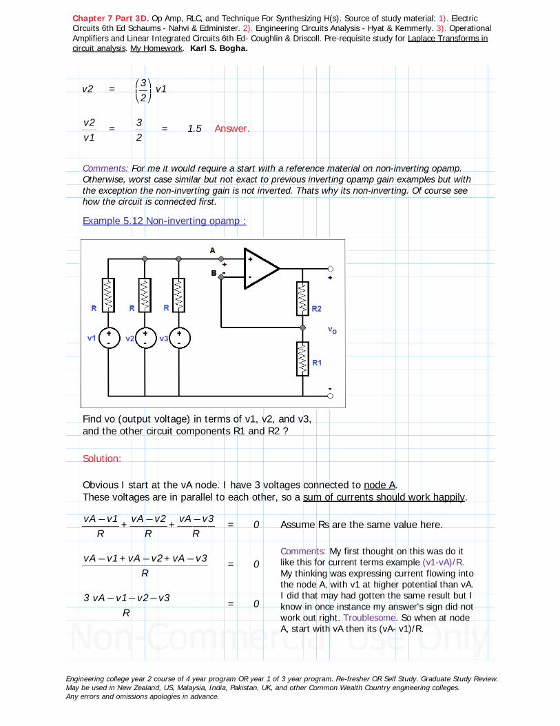
Chapter 7 Part 3D. Op Amp, RLC, and Technique For Synthesizing H(s). Source of study material: 1). Electric Circuits 6th Ed Schaums - Nahvi & Edminister. 2). Engineering Circuits Analysis - Hyat & Kemmerly. 3). Operational Amplifiers and Linear Integrated Circuits 6th Ed- Coughlin & Driscoll. Pre-requisite study for Laplace Transforms in circuit analysis. My Homework. Karl S. Bogha.
v2 = ⎛⎜⎝―32⎞⎟⎠
v1
―v2v1
= ―32
= 1.5 Answer.
Comments: For me it would require a start with a reference material on non-inverting opamp. Otherwise, worst case similar but not exact to previous inverting opamp gain examples but with the exception the non-inverting gain is not inverted. Thats why its non-inverting. Of course see how the circuit is connected first.
Example 5.12 Non-inverting opamp :
Find vo (output voltage) in terms of v1, v2, and v3, and the other circuit components R1 and R2 ?
Solution:
Obvious I start at the vA node. I have 3 voltages connected to node A.These voltages are in parallel to each other, so a sum of currents should work happily.
++―――−vA v1R
―――−vA v2R
―――−vA v3R
= 0 Assume Rs are the same value here.
Comments: My first thought on this was do it like this for current terms example (v1-vA)/R.My thinking was expressing current flowing into the node A, with v1 at higher potential than vA. I did that may had gotten the same result but I know in once instance my answer's sign did not work out right. Troublesome. So when at node A, start with vA then its (vA- v1)/R.
―――――――――−+−+−vA v1 vA v2 vA v3
R= 0
――――――−−−3 vA v1 v2 v3
R= 0
Engineering college year 2 course of 4 year program OR year 1 of 3 year program. Re-fresher OR Self Study. Graduate Study Review.May be used in New Zealand, US, Malaysia, India, Pakistan, UK, and other Common Wealth Country engineering colleges.Any errors and omissions apologies in advance.

Chapter 7 Part 3D. Op Amp, RLC, and Technique For Synthesizing H(s). Source of study material: 1). Electric Circuits 6th Ed Schaums - Nahvi & Edminister. 2). Engineering Circuits Analysis - Hyat & Kemmerly. 3). Operational Amplifiers and Linear Integrated Circuits 6th Ed- Coughlin & Driscoll. Pre-requisite study for Laplace Transforms in circuit analysis. My Homework. Karl S. Bogha.
――――++v1 v2 v3
R= ――
3 vAR
――――++v1 v2 v3
R= ――
3 vAR
Now R can be removed its the only common denominator on both sides.
++v1 v2 v3 = 3 vA
vA = ―13
(( ++v1 v2 v3))
Solved for vA, need to get an expression with vA that include vo.
Gain? Circuit gain expression.
Alright, I re-arrange the circuit to get that gain. Because the way the circuit is connected its a little different-difficult to see the gain on this non-inverting opamp.
Correct. Notes in the figure above. I can apply the gain expression.
――vovA
= ⎛⎜⎝
+1 ――R2R1⎞⎟⎠
Engineering college year 2 course of 4 year program OR year 1 of 3 year program. Re-fresher OR Self Study. Graduate Study Review.May be used in New Zealand, US, Malaysia, India, Pakistan, UK, and other Common Wealth Country engineering colleges.Any errors and omissions apologies in advance.
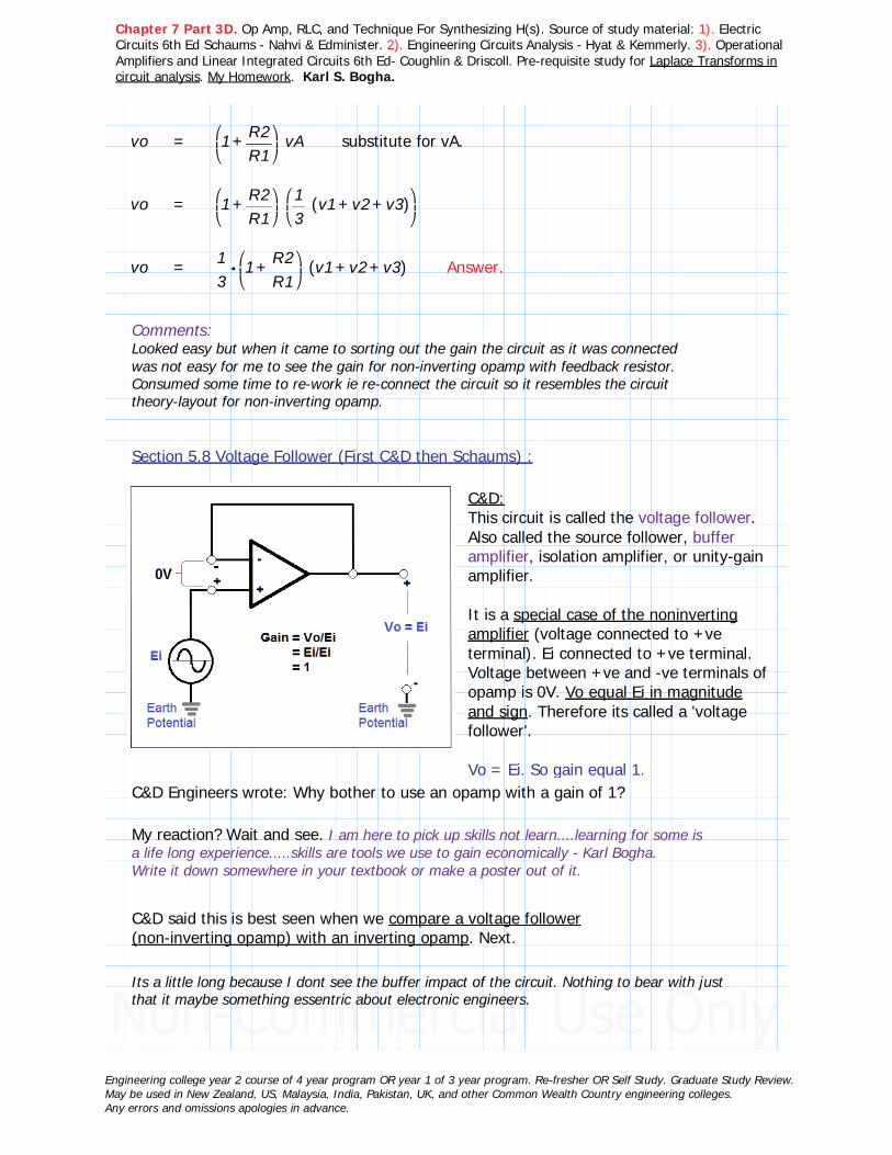
Chapter 7 Part 3D. Op Amp, RLC, and Technique For Synthesizing H(s). Source of study material: 1). Electric Circuits 6th Ed Schaums - Nahvi & Edminister. 2). Engineering Circuits Analysis - Hyat & Kemmerly. 3). Operational Amplifiers and Linear Integrated Circuits 6th Ed- Coughlin & Driscoll. Pre-requisite study for Laplace Transforms in circuit analysis. My Homework. Karl S. Bogha.
vo = ⎛⎜⎝
+1 ――R2R1⎞⎟⎠
vA substitute for vA.
vo = ⎛⎜⎝
+1 ――R2R1⎞⎟⎠⎛⎜⎝―13
(( ++v1 v2 v3))⎞⎟⎠
vo = ⋅―13⎛⎜⎝
+1 ――R2R1⎞⎟⎠
(( ++v1 v2 v3)) Answer.
Comments:Looked easy but when it came to sorting out the gain the circuit as it was connected was not easy for me to see the gain for non-inverting opamp with feedback resistor. Consumed some time to re-work ie re-connect the circuit so it resembles the circuit theory-layout for non-inverting opamp.
Section 5.8 Voltage Follower (First C&D then Schaums) :
C&D:This circuit is called the voltage follower. Also called the source follower, buffer amplifier, isolation amplifier, or unity-gain amplifier.
It is a special case of the noninverting amplifier (voltage connected to +ve terminal). Ei connected to +ve terminal. Voltage between +ve and -ve terminals of opamp is 0V. Vo equal Ei in magnitude and sign. Therefore its called a 'voltage follower'.
Vo = Ei. So gain equal 1.C&D Engineers wrote: Why bother to use an opamp with a gain of 1?
My reaction? Wait and see. I am here to pick up skills not learn....learning for some is a life long experience.....skills are tools we use to gain economically - Karl Bogha. Write it down somewhere in your textbook or make a poster out of it.
C&D said this is best seen when we compare a voltage follower (non-inverting opamp) with an inverting opamp. Next.
Its a little long because I dont see the buffer impact of the circuit. Nothing to bear with just that it maybe something essentric about electronic engineers.
Engineering college year 2 course of 4 year program OR year 1 of 3 year program. Re-fresher OR Self Study. Graduate Study Review.May be used in New Zealand, US, Malaysia, India, Pakistan, UK, and other Common Wealth Country engineering colleges.Any errors and omissions apologies in advance.
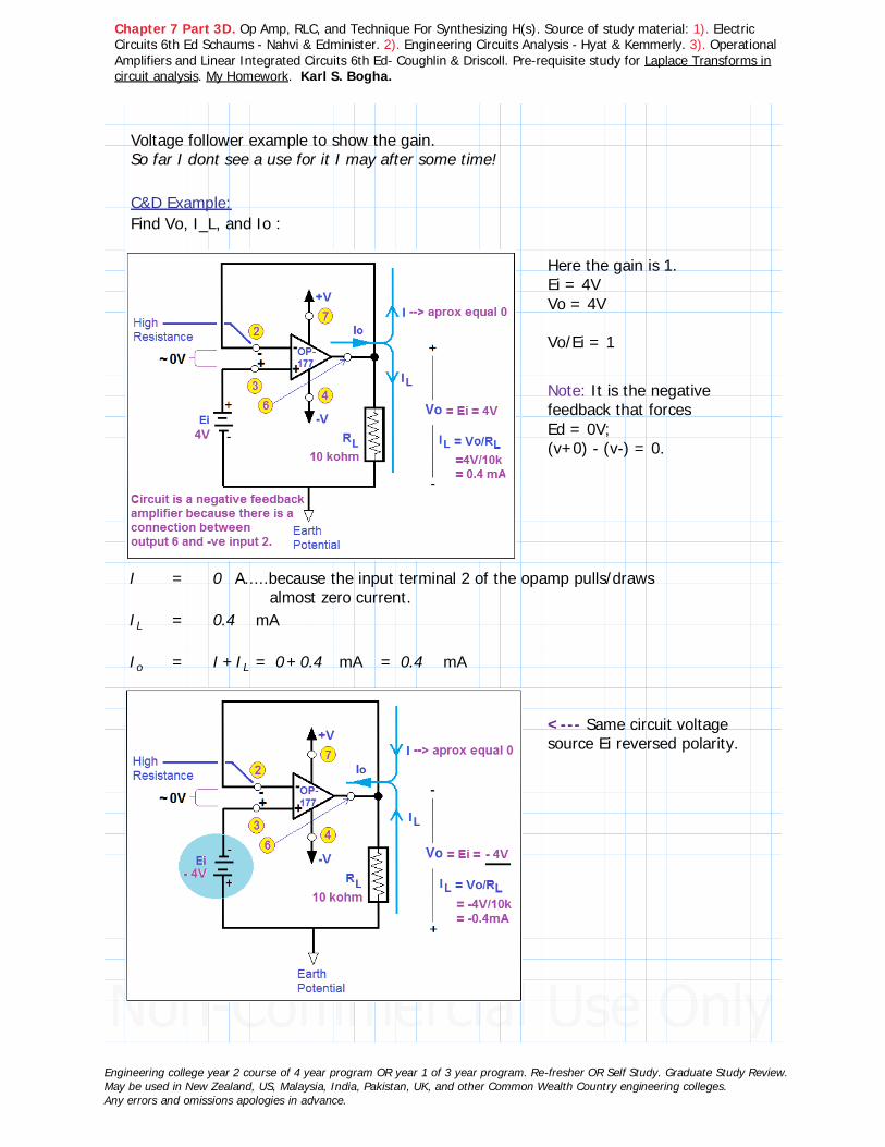
Chapter 7 Part 3D. Op Amp, RLC, and Technique For Synthesizing H(s). Source of study material: 1). Electric Circuits 6th Ed Schaums - Nahvi & Edminister. 2). Engineering Circuits Analysis - Hyat & Kemmerly. 3). Operational Amplifiers and Linear Integrated Circuits 6th Ed- Coughlin & Driscoll. Pre-requisite study for Laplace Transforms in circuit analysis. My Homework. Karl S. Bogha.
Voltage follower example to show the gain. So far I dont see a use for it I may after some time!
C&D Example:Find Vo, I_L, and Io :
Here the gain is 1.Ei = 4VVo = 4V
Vo/Ei = 1
Note: It is the negative feedback that forces Ed = 0V;(v+0) - (v-) = 0.
I = 0 A.....because the input terminal 2 of the opamp pulls/draws almost zero current.
IL = 0.4 mA
Io = +I IL = +0 0.4 mA = 0.4 mA
<--- Same circuit voltage source Ei reversed polarity.
Engineering college year 2 course of 4 year program OR year 1 of 3 year program. Re-fresher OR Self Study. Graduate Study Review.May be used in New Zealand, US, Malaysia, India, Pakistan, UK, and other Common Wealth Country engineering colleges.Any errors and omissions apologies in advance.

Chapter 7 Part 3D. Op Amp, RLC, and Technique For Synthesizing H(s). Source of study material: 1). Electric Circuits 6th Ed Schaums - Nahvi & Edminister. 2). Engineering Circuits Analysis - Hyat & Kemmerly. 3). Operational Amplifiers and Linear Integrated Circuits 6th Ed- Coughlin & Driscoll. Pre-requisite study for Laplace Transforms in circuit analysis. My Homework. Karl S. Bogha.
Explanation next from C&D is not on the gain or the output voltage polarity, rather the input loading effect. This is the resistance seen at the input terminals of the opamp. First opamp circuit is non-inverted, followed by a inverted circuit.
A signal generator is connected to the non-inverting (+ve) terminal.Signal generator has a high internal resitance 90 kohm.The generator voltage is 1V.
≔I =―――1
⋅90 103⋅11.11 10−6
I aprox equal 10 uA
The input terminal of the opamp draws (pulls) a small current from the signal generator. Current I is 10 uA, the voltage drop across Rint will be
≔vRint =⋅⋅⋅10 10−6 90 103 0.9 V
The opamp internal resistance, at terminal +ve and -ve is infinite. Very high resitance (many megaohms), hence the opamp cannot draw/pull current, at most a negligible current passes. Since, the opamp is pulling a negligible current the actual current passing thru Rint now will be much smaller than 10uA, and the voltage drop across Rint will be much smaller than 0.9V. Instead it will be 0V, negligible. Agreed.
The terminal voltage Ei of signal source, ie the terminals outside of the signal generator shown in figure above, become the input voltage to the opamp and equals Egen.Ei = Egen. Hence Vo = Ei = Egen.
Vo = Ei = EgenAs shown in the figure above.
Engineering college year 2 course of 4 year program OR year 1 of 3 year program. Re-fresher OR Self Study. Graduate Study Review.May be used in New Zealand, US, Malaysia, India, Pakistan, UK, and other Common Wealth Country engineering colleges.Any errors and omissions apologies in advance.

Chapter 7 Part 3D. Op Amp, RLC, and Technique For Synthesizing H(s). Source of study material: 1). Electric Circuits 6th Ed Schaums - Nahvi & Edminister. 2). Engineering Circuits Analysis - Hyat & Kemmerly. 3). Operational Amplifiers and Linear Integrated Circuits 6th Ed- Coughlin & Driscoll. Pre-requisite study for Laplace Transforms in circuit analysis. My Homework. Karl S. Bogha.
Now I study the similar circuit connected to the non-inverting opamp terminal.It has a feedback resistor, the previous circuit had no feedback resistor. Point made, previously, was Vo = Ei which Ei = Egen beause the opamp is not pulling any current (negligible). Agreed. So I say there the gain was 1. The non-inverting opamp here has a gain of -1. There is an additional input resistance Ri, this is not internal resitance to the signal generator rather an additional resistance Ri.I noticed no Ri was applied in the non-inverting opamp? Troubling. Yes. Why? I try to explain, my attempt.Ri input resistance applied to inverting opamp -ve terminal. When we have 2 dc batteries, wires and a lamp load, expect current to flow from load into battery -ve terminal then out +ve terminal, not the other way. Same. So Ri is placed connected to the -ve terminal. This was not possible in the previous non-inverting circuit beause Ri would connect to +ve terminal.
Rint and Ri are in series. The signal generator +ve terminal is connected in series to Rint and Ri, then to the -ve terminal then thru the +ve terminal of the opamp and then to earth. That makes the loop back to the -ve terminal of the signal generator.
The voltage available from the signal generator to the external circuit is the voltage drop across Ri. Correct.
Engineering college year 2 course of 4 year program OR year 1 of 3 year program. Re-fresher OR Self Study. Graduate Study Review.May be used in New Zealand, US, Malaysia, India, Pakistan, UK, and other Common Wealth Country engineering colleges.Any errors and omissions apologies in advance.

Chapter 7 Part 3D. Op Amp, RLC, and Technique For Synthesizing H(s). Source of study material: 1). Electric Circuits 6th Ed Schaums - Nahvi & Edminister. 2). Engineering Circuits Analysis - Hyat & Kemmerly. 3). Operational Amplifiers and Linear Integrated Circuits 6th Ed- Coughlin & Driscoll. Pre-requisite study for Laplace Transforms in circuit analysis. My Homework. Karl S. Bogha.
So now I have the voltage available across the signal generator terminals, as shown in the non-inverting circuit, which is:
Ei = ⋅⎛⎜⎝―――
Ri
+Rint Ri
⎞⎟⎠
Egen
≔Rint ⋅90 103 ≔Ri ⋅10 103 ≔Εgen 1.0
Ei = =⋅⎛⎜⎝―――
Ri
+Rint Ri
⎞⎟⎠
1.0 0.1 V
0.1V is the input voltage to the non-inverting opamp.
The input voltage 0.1V, with the gain is -1, the output voltage Vo equal:
Vo = =⋅((0.1)) ((−1)) −0.1 V
Going back early in the inverting opamp topic, circuit with Rf, the closed loop gain was Acl = Vo/Ei = - Rf/Ri
ACL = ―Vo
Ei= −―
Rf
Ri
Now, with the high impedance signal source, the high impedance being Rint,the internal resitance of the signal generator, ie the closed loop gain Acl must be revised to include Rint:
ACL = ―Vo
Ei= −
⎛⎜⎝―――
Rf
+Rint Ri
⎞⎟⎠
Here in this inverting opamp circuit:
≔Rint ⋅90 103 ≔Ri ⋅10 103 ≔Rf ⋅10 103
ACL = =−⎛⎜⎝―――
Rf
+Rint Ri
⎞⎟⎠−0.1
See figure on next page for circuit identified to main parts.
Engineering college year 2 course of 4 year program OR year 1 of 3 year program. Re-fresher OR Self Study. Graduate Study Review.May be used in New Zealand, US, Malaysia, India, Pakistan, UK, and other Common Wealth Country engineering colleges.Any errors and omissions apologies in advance.
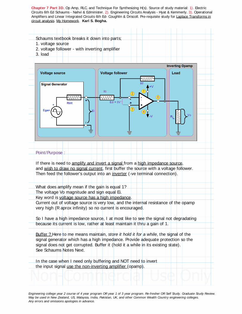
Chapter 7 Part 3D. Op Amp, RLC, and Technique For Synthesizing H(s). Source of study material: 1). Electric Circuits 6th Ed Schaums - Nahvi & Edminister. 2). Engineering Circuits Analysis - Hyat & Kemmerly. 3). Operational Amplifiers and Linear Integrated Circuits 6th Ed- Coughlin & Driscoll. Pre-requisite study for Laplace Transforms in circuit analysis. My Homework. Karl S. Bogha.
Schaums textbook breaks it down into parts; 1. voltage source2. voltage follower - with inverting amplifier3. load
Point/Purpose :
If there is need to amplify and invert a signal from a high impedance source,and wish to draw no signal current, first buffer the source with a voltage follower. Then feed the follower's output into an inverter (-ve terminal connection).
What does amplify mean if the gain is equal 1? The voltage Vo magnitude and sign equal Ei.Key word is voltage source has a high impedance.Current out of voltage source is very low, and the internal resistance of the opamp very high (R aprox infinity) so no current is encouraged.
So I have a high impedance source, I at most like to see the signal not degradating because its current is low, rather at least maintain it thru a gain of 1.
Buffer ? Here to me means maintain, store it hold it for a while, the signal of the signal generator which has a high impedance. Provide adequate protection so the signal does not get corrupted. Buffer it (hold it a while in its existing state).See Schaums Notes Next.
In the case when I need only buffering and NOT need to invert the input signal use the non-inverting amplifier (opamp).
Engineering college year 2 course of 4 year program OR year 1 of 3 year program. Re-fresher OR Self Study. Graduate Study Review.May be used in New Zealand, US, Malaysia, India, Pakistan, UK, and other Common Wealth Country engineering colleges.Any errors and omissions apologies in advance.

Chapter 7 Part 3D. Op Amp, RLC, and Technique For Synthesizing H(s). Source of study material: 1). Electric Circuits 6th Ed Schaums - Nahvi & Edminister. 2). Engineering Circuits Analysis - Hyat & Kemmerly. 3). Operational Amplifiers and Linear Integrated Circuits 6th Ed- Coughlin & Driscoll. Pre-requisite study for Laplace Transforms in circuit analysis. My Homework. Karl S. Bogha.
Now I study the Schaums notes on Voltage Follower. Something closer to making buffer.
Schaums:
The circuit above provides a unity gain amplifier.Here v2 = v1, since v1 = v+ v2 = v - and v+ = v -.Following the circuit connection above shows that.
In this circuit connection,the output v2 equal the input v1.OR regardless of the waveform of v1, the output v2 follows v1.
The circuit's resistor R_L is the load.Current is supplied by the output of the opamp and the feedback connection.This current is i_L. Current i_L is supplied by the voltage follower circuitry.The current i_L is a relief for the voltage source because its supplied thru the voltage follower.
Resistor R_L is a load to voltage source. Because the voltage follower is in the middle, it isolates the load from the source. The voltage follower supplies i_L to the load R_L, the opamp eliminates the loading effect of R_L on the voltage source. Now, by that, the voltage follower functions as a buffer.
Comment: I am not a pioneer design electronic engineer, thats why I found buffer misleading. Plus it plays more of isolate than buffer. There maybe a technical application for that, but most all circuits have intermediate steps in electronic. I may been looking for a digital storage buffer circuit understanding. Here the aim was to relief the load RL directly from the source and connect it to an intermediate circuitry using an opamp to provide the buffer.
Engineering college year 2 course of 4 year program OR year 1 of 3 year program. Re-fresher OR Self Study. Graduate Study Review.May be used in New Zealand, US, Malaysia, India, Pakistan, UK, and other Common Wealth Country engineering colleges.Any errors and omissions apologies in advance.

Chapter 7 Part 3D. Op Amp, RLC, and Technique For Synthesizing H(s). Source of study material: 1). Electric Circuits 6th Ed Schaums - Nahvi & Edminister. 2). Engineering Circuits Analysis - Hyat & Kemmerly. 3). Operational Amplifiers and Linear Integrated Circuits 6th Ed- Coughlin & Driscoll. Pre-requisite study for Laplace Transforms in circuit analysis. My Homework. Karl S. Bogha.
Example 5.13 :
a). Find i_s, v_l, v2, and v1. Circuit provided in solution.
b). Compare these results with those obtained when source and load are connected directly. Circuit provided in solution
Solution:
a). This is the circuit layout provided with the question.
is = 0 voltage source internal resistance is high so current is negligible.
v1 = vs voltage drop across Rs is negligible because i_s is near 0.therefore v1 equals v_s.
v2 = v1 voltage at opamp output terminal (6) is the same as the voltage at inverting terminal (2). There is no feedback resistor hence no voltdrop.
Now, in this condition :
v2 = v1 = vs Voltage across R_L is vL; vl = v2
Hence il = ―vs
RlA. We would had v2/R_L but the point is to show v_s is the same as v2.
Because the opamp does not pull/draw any current from v_s, hence,v_s reaches the load R_L with no reduction caused by load current i_L.
What is the source of the current i_L in R_L ? Opamp is the source of the current.Its not i_s that's the current source because current there is negligible.
Engineering college year 2 course of 4 year program OR year 1 of 3 year program. Re-fresher OR Self Study. Graduate Study Review.May be used in New Zealand, US, Malaysia, India, Pakistan, UK, and other Common Wealth Country engineering colleges.Any errors and omissions apologies in advance.

Chapter 7 Part 3D. Op Amp, RLC, and Technique For Synthesizing H(s). Source of study material: 1). Electric Circuits 6th Ed Schaums - Nahvi & Edminister. 2). Engineering Circuits Analysis - Hyat & Kemmerly. 3). Operational Amplifiers and Linear Integrated Circuits 6th Ed- Coughlin & Driscoll. Pre-requisite study for Laplace Transforms in circuit analysis. My Homework. Karl S. Bogha.
b). This is the circuit layout provided with the question.
In this circuit connection the opamp is removed.
Voltage source is directly connected to load.R_s has a high resistance. Very high.Negligible current flows out from v_s.Therefore whatever i_s is its equal to ? i_L.
is = il =⎛⎜⎝―――
vs
+Rl Rs
⎞⎟⎠
v1 = v2 = ⋅⎛⎜⎝―――
Rl
+Rl Rs
⎞⎟⎠
vs
Now in this case current is drawn/pulled by R_L from the source v_s, this same current goes thru R_s.But now i_s is not negligible as it was prior, since i_s = i_L.
Because Rs resistance is so high, there may not be appreciable volt drop across Rs?No, that was my hang-up. The same current flows thru Rs. Back to basic circuits.The benefit here is in the part a of the circuit.
Engineering college year 2 course of 4 year program OR year 1 of 3 year program. Re-fresher OR Self Study. Graduate Study Review.May be used in New Zealand, US, Malaysia, India, Pakistan, UK, and other Common Wealth Country engineering colleges.Any errors and omissions apologies in advance.

Chapter 7 Part 3D. Op Amp, RLC, and Technique For Synthesizing H(s). Source of study material: 1). Electric Circuits 6th Ed Schaums - Nahvi & Edminister. 2). Engineering Circuits Analysis - Hyat & Kemmerly. 3). Operational Amplifiers and Linear Integrated Circuits 6th Ed- Coughlin & Driscoll. Pre-requisite study for Laplace Transforms in circuit analysis. My Homework. Karl S. Bogha.
Section 5.9 Differential And Difference Amplifiers
Arrows shown as in Schaums supplement textbook.
Differential amplifier.
Signal source vf has no connection to earth.This source is called a floating source.
Both terminals, inverting and non-inverting, of the opamp are connected.First time here.
Voltage across terminals A and B are the same: - Measuring the voltage on the negative terminal side of R1s.OR - Measuring the voltage on the positive terminals of R2s.
KVL for the opamp input loop:vf = +iR1 iR1 = 2 R1i
i = ――vf
2 R1
Next KVL around the opamp.
Engineering college year 2 course of 4 year program OR year 1 of 3 year program. Re-fresher OR Self Study. Graduate Study Review.May be used in New Zealand, US, Malaysia, India, Pakistan, UK, and other Common Wealth Country engineering colleges.Any errors and omissions apologies in advance.

Chapter 7 Part 3D. Op Amp, RLC, and Technique For Synthesizing H(s). Source of study material: 1). Electric Circuits 6th Ed Schaums - Nahvi & Edminister. 2). Engineering Circuits Analysis - Hyat & Kemmerly. 3). Operational Amplifiers and Linear Integrated Circuits 6th Ed- Coughlin & Driscoll. Pre-requisite study for Laplace Transforms in circuit analysis. My Homework. Karl S. Bogha.
Opamp loop: Current i flows thru the node B, then thru R2, then at the output terminal and down to the earth ref, then up thru R2 connected to node A, then thru the opamp and back to node B.
I assume load connected across terminals vo has no impedance no voltage drop its just the voltage measured at opamp output terminal.
++vo iR2 iR2 = 0
vo = −2 R2i
Substitute i in the expression above.
vo = −2 R2 ⎛⎜⎝――
vf2 R1
⎞⎟⎠
= −⎛⎜⎝――R2R1⎞⎟⎠
vf <---
I can have 2 voltage sources each connected to earth, with one source connected to the inverting and the other non-inverting terminal of the opamp.
Circuit with 2 earthed voltage sources.
vo = −v1 v2
Difference AmplifierORSubtractor Amplifier.
Here vo equal: vo = −⎛⎜⎝――R2R1⎞⎟⎠
vf = ⋅−⎛⎜⎝――R2R1⎞⎟⎠
(( −v1 v2)) <---
vo = ⋅⎛⎜⎝――R2R1⎞⎟⎠
(( −v2 v1)) <--- with a positive sign infront.
Schaums example 14 was not agreable to me. Hours...days..nights..spent and did not result with the correct solution. Thats why its not there. Checking with C&D their difference amplifier uses multiple opamps, that's ok, just that I need an example I can work. So if permitting I may do the C&D example later.
Engineering college year 2 course of 4 year program OR year 1 of 3 year program. Re-fresher OR Self Study. Graduate Study Review.May be used in New Zealand, US, Malaysia, India, Pakistan, UK, and other Common Wealth Country engineering colleges.Any errors and omissions apologies in advance.

Chapter 7 Part 3D. Op Amp, RLC, and Technique For Synthesizing H(s). Source of study material: 1). Electric Circuits 6th Ed Schaums - Nahvi & Edminister. 2). Engineering Circuits Analysis - Hyat & Kemmerly. 3). Operational Amplifiers and Linear Integrated Circuits 6th Ed- Coughlin & Driscoll. Pre-requisite study for Laplace Transforms in circuit analysis. My Homework. Karl S. Bogha.
Section 5.10 Circuits Containing Several Opamps.
A circuit can have multiple opamps.The opamps can be in cascade (back to back) or nested loops, because there is no loading effect. The loading effect I got some understanding in the Voltage Follower circuit.The design and analysis is the same.
Example 5.15 (Multiple Opamps) :
Solution:Opamp in front to the left is an inverting opamp.The second opamp is also an inverting opamp.
Since resistors are all in kilohom, 10^3 may be dropped, depending on the math operation and units.Voltage supply to the first opamp is -0.6V.
vo_1 = ⋅−Ei1⎛⎜⎝――Rf1
Ri1
⎞⎟⎠
This formula from inverting opamp theory or reading section.Reading section just dont make it because it requires the apprentice to practice a skill from the study material. Lets just say theory, its not the best but better than reading!
≔Rf1 3 ≔Ri1 1 ≔Ei1 −0.6
vo_1 = =⋅−Ei1⎛⎜⎝――Rf1
Ri1
⎞⎟⎠
1.8 V
Engineering college year 2 course of 4 year program OR year 1 of 3 year program. Re-fresher OR Self Study. Graduate Study Review.May be used in New Zealand, US, Malaysia, India, Pakistan, UK, and other Common Wealth Country engineering colleges.Any errors and omissions apologies in advance.

Chapter 7 Part 3D. Op Amp, RLC, and Technique For Synthesizing H(s). Source of study material: 1). Electric Circuits 6th Ed Schaums - Nahvi & Edminister. 2). Engineering Circuits Analysis - Hyat & Kemmerly. 3). Operational Amplifiers and Linear Integrated Circuits 6th Ed- Coughlin & Driscoll. Pre-requisite study for Laplace Transforms in circuit analysis. My Homework. Karl S. Bogha.
The 2nd opamp is an adder or summing circuit.
1 and 2 kohm in parallel, then the other 2 kohm which makes the feedback.
vo = −⎛⎜⎝
‥++⎛⎜⎝―Rf
R1
⎞⎟⎠
v1⎛⎜⎝―Rf
R2
⎞⎟⎠
v2 ' .⎞⎟⎠
≔v1 0.5 ≔v2 1.8 ≔Rf 2 ≔R1 1 ≔R2 2
vo = =−⎛⎜⎝
+⋅⎛⎜⎝―Rf
R1
⎞⎟⎠
v1 ⋅⎛⎜⎝―Rf
R2
⎞⎟⎠
v2⎞⎟⎠−2.8 V
Comments: That looked simple enough. For me I had some difficulty where the summing resistor 1 kohm connected to the 2 kohm at the top. After a little study I found that the parallel resistors were in parallel forming the summer, and Rf was of to the other side...in series to both R1 and R2. Next the formulas I had not used in a few days. Then of course the vo from opamp 1 is the input voltage for the 2 kohm resistor. After sorting that straight use of formulas.
Next example complicated for me, some skills there.
Engineering college year 2 course of 4 year program OR year 1 of 3 year program. Re-fresher OR Self Study. Graduate Study Review.May be used in New Zealand, US, Malaysia, India, Pakistan, UK, and other Common Wealth Country engineering colleges.Any errors and omissions apologies in advance.

Chapter 7 Part 3D. Op Amp, RLC, and Technique For Synthesizing H(s). Source of study material: 1). Electric Circuits 6th Ed Schaums - Nahvi & Edminister. 2). Engineering Circuits Analysis - Hyat & Kemmerly. 3). Operational Amplifiers and Linear Integrated Circuits 6th Ed- Coughlin & Driscoll. Pre-requisite study for Laplace Transforms in circuit analysis. My Homework. Karl S. Bogha.
Example 5.16 (Multiple Opamps) :
Let Rs = 1 kohm in the circuit.Find v1, v2, vo, i_s, i_1, and i_f as a function of v_s for
a). Rf = infinity
b). Rf = 40 kohm
Solution:
a). Rf = Infinity
Voltage at point B = v1? Is voltage past the resistor Rs = 1 kohm, which is the voltage remaining in the series circuit, ie over the R = 5 kohm resistor.Voltage at v+ terminal of the 1st opamp is 0V same for the 2nd, both connected to earth (0V ref).
Engineering college year 2 course of 4 year program OR year 1 of 3 year program. Re-fresher OR Self Study. Graduate Study Review.May be used in New Zealand, US, Malaysia, India, Pakistan, UK, and other Common Wealth Country engineering colleges.Any errors and omissions apologies in advance.
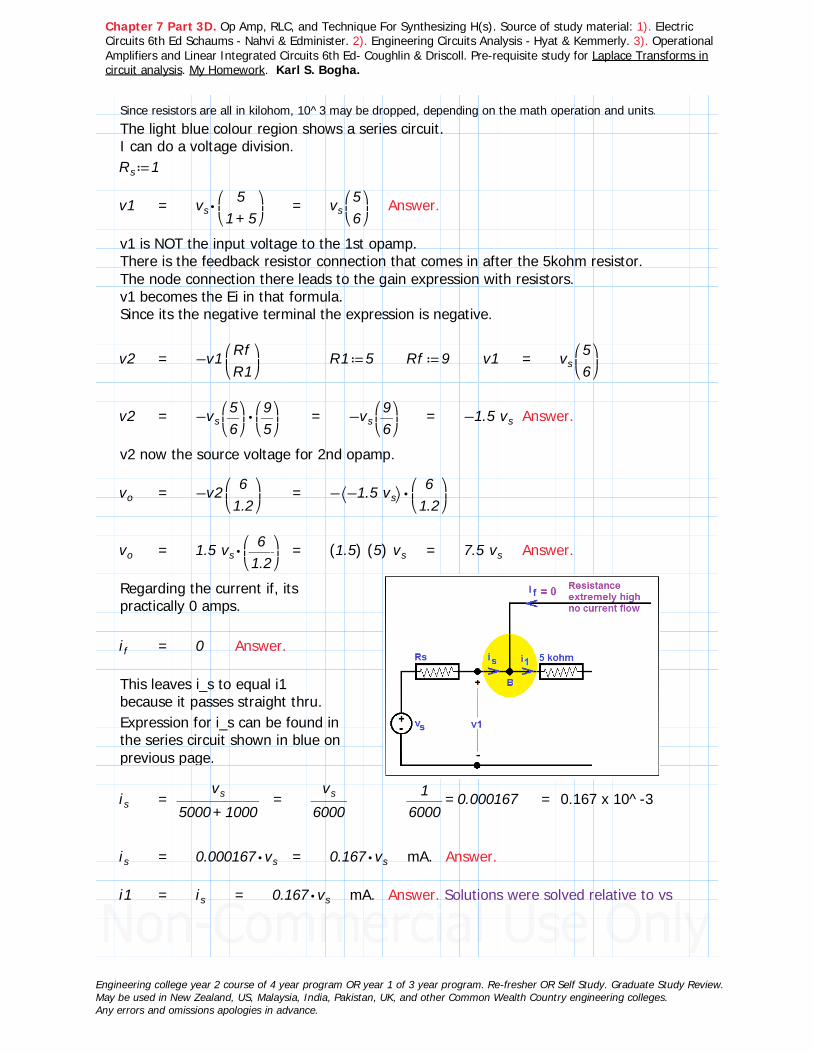
Chapter 7 Part 3D. Op Amp, RLC, and Technique For Synthesizing H(s). Source of study material: 1). Electric Circuits 6th Ed Schaums - Nahvi & Edminister. 2). Engineering Circuits Analysis - Hyat & Kemmerly. 3). Operational Amplifiers and Linear Integrated Circuits 6th Ed- Coughlin & Driscoll. Pre-requisite study for Laplace Transforms in circuit analysis. My Homework. Karl S. Bogha.
Since resistors are all in kilohom, 10^3 may be dropped, depending on the math operation and units.The light blue colour region shows a series circuit.I can do a voltage division.≔Rs 1
v1 = ⋅vs⎛⎜⎝――
5+1 5⎞⎟⎠
= vs⎛⎜⎝―56⎞⎟⎠
Answer.
v1 is NOT the input voltage to the 1st opamp. There is the feedback resistor connection that comes in after the 5kohm resistor. The node connection there leads to the gain expression with resistors.v1 becomes the Ei in that formula. Since its the negative terminal the expression is negative.
v2 = −v1 ⎛⎜⎝――RfR1⎞⎟⎠
≔R1 5 ≔Rf 9 v1 = vs⎛⎜⎝―56⎞⎟⎠
v2 = ⋅−vs⎛⎜⎝―56⎞⎟⎠⎛⎜⎝―95⎞⎟⎠
= −vs⎛⎜⎝―96⎞⎟⎠
= −1.5 vs Answer.
v2 now the source voltage for 2nd opamp.
vo = −v2 ⎛⎜⎝――
61.2⎞⎟⎠
= ⋅−⎛⎝−1.5 vs⎞⎠⎛⎜⎝――
61.2⎞⎟⎠
vo = ⋅1.5 vs⎛⎜⎝――
61.2⎞⎟⎠
= ((1.5)) ((5)) vs = 7.5 vs Answer.
Regarding the current if, its practically 0 amps.
if = 0 Answer.
This leaves i_s to equal i1 because it passes straight thru.Expression for i_s can be found in the series circuit shown in blue on previous page.
is = ――――vs
+5000 1000= ――
vs
6000=――
16000
0.000167 = 0.167 x 10^-3
is = ⋅0.000167 vs = ⋅0.167 vs mA. Answer.
i1 = is = ⋅0.167 vs mA. Answer. Solutions were solved relative to vs
Engineering college year 2 course of 4 year program OR year 1 of 3 year program. Re-fresher OR Self Study. Graduate Study Review.May be used in New Zealand, US, Malaysia, India, Pakistan, UK, and other Common Wealth Country engineering colleges.Any errors and omissions apologies in advance.
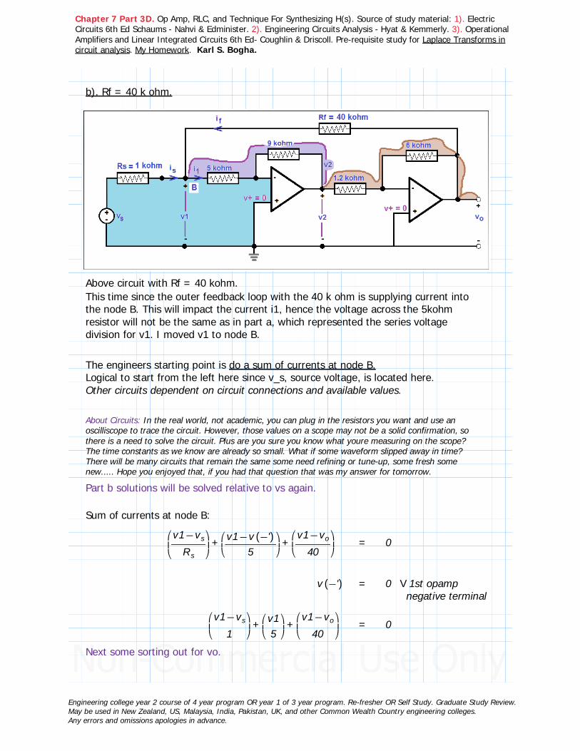
Chapter 7 Part 3D. Op Amp, RLC, and Technique For Synthesizing H(s). Source of study material: 1). Electric Circuits 6th Ed Schaums - Nahvi & Edminister. 2). Engineering Circuits Analysis - Hyat & Kemmerly. 3). Operational Amplifiers and Linear Integrated Circuits 6th Ed- Coughlin & Driscoll. Pre-requisite study for Laplace Transforms in circuit analysis. My Homework. Karl S. Bogha.
b). Rf = 40 k ohm.
Above circuit with Rf = 40 kohm.This time since the outer feedback loop with the 40 k ohm is supplying current into the node B. This will impact the current i1, hence the voltage across the 5kohm resistor will not be the same as in part a, which represented the series voltage division for v1. I moved v1 to node B.
The engineers starting point is do a sum of currents at node B.Logical to start from the left here since v_s, source voltage, is located here.Other circuits dependent on circuit connections and available values.
About Circuits: In the real world, not academic, you can plug in the resistors you want and use an oscilliscope to trace the circuit. However, those values on a scope may not be a solid confirmation, so there is a need to solve the circuit. Plus are you sure you know what youre measuring on the scope? The time constants as we know are already so small. What if some waveform slipped away in time? There will be many circuits that remain the same some need refining or tune-up, some fresh some new..... Hope you enjoyed that, if you had that question that was my answer for tomorrow.
Part b solutions will be solved relative to vs again.
Sum of currents at node B:
++⎛⎜⎝―――−v1 vs
Rs
⎞⎟⎠⎛⎜⎝――――−v1 v ((−'))
5⎞⎟⎠⎛⎜⎝―――−v1 vo
40⎞⎟⎠
= 0
v ((−')) = 0 V 1st opamp negative terminal
++⎛⎜⎝―――−v1 vs
1⎞⎟⎠⎛⎜⎝―v15⎞⎟⎠⎛⎜⎝―――−v1 vo
40⎞⎟⎠
= 0
Next some sorting out for vo.
Engineering college year 2 course of 4 year program OR year 1 of 3 year program. Re-fresher OR Self Study. Graduate Study Review.May be used in New Zealand, US, Malaysia, India, Pakistan, UK, and other Common Wealth Country engineering colleges.Any errors and omissions apologies in advance.

Chapter 7 Part 3D. Op Amp, RLC, and Technique For Synthesizing H(s). Source of study material: 1). Electric Circuits 6th Ed Schaums - Nahvi & Edminister. 2). Engineering Circuits Analysis - Hyat & Kemmerly. 3). Operational Amplifiers and Linear Integrated Circuits 6th Ed- Coughlin & Driscoll. Pre-requisite study for Laplace Transforms in circuit analysis. My Homework. Karl S. Bogha.
The circuit connection explanation above shows 40 k ohm Rf is not relevant for vo when using the expression vo = Ei (Rf/Ri). The Rf is 6 k ohm the 40 k ohm resistor does not form a feedback loop. Correct.
The input voltage Ei or vi for 2nd opamp equal v2.
vo = −v2 ⎛⎜⎝――
61.2⎞⎟⎠
= −5 v2
Going one opamp back to the 1st opamp:
v2 = −v1 ⎛⎜⎝―95⎞⎟⎠
Note: v2/v1 = - Rf/R1 = - 9/5.
Substitute v2 in the vo expression.
vo = −⎛⎜⎝−v1 ⎛⎜⎝
―95⎞⎟⎠⎞⎟⎠⎛⎜⎝――
61.2⎞⎟⎠
= 9 v1
vo = 9 v1
Substitute vo in the expression below I got previosly from sum of currents.
++⎛⎜⎝―――−v1 vs
1⎞⎟⎠⎛⎜⎝―v15⎞⎟⎠⎛⎜⎝―――−v1 vo
40⎞⎟⎠
= 0
++⎛⎜⎝―――−v1 vs
1⎞⎟⎠⎛⎜⎝―v15⎞⎟⎠⎛⎜⎝―――−v1 9 v140
⎞⎟⎠
= 0
−++−40 v1 40 vs 8 v1 v1 9 v1 = 0
−40 v1 40 vs = 0
v1 = vs
Engineering college year 2 course of 4 year program OR year 1 of 3 year program. Re-fresher OR Self Study. Graduate Study Review.May be used in New Zealand, US, Malaysia, India, Pakistan, UK, and other Common Wealth Country engineering colleges.Any errors and omissions apologies in advance.

Chapter 7 Part 3D. Op Amp, RLC, and Technique For Synthesizing H(s). Source of study material: 1). Electric Circuits 6th Ed Schaums - Nahvi & Edminister. 2). Engineering Circuits Analysis - Hyat & Kemmerly. 3). Operational Amplifiers and Linear Integrated Circuits 6th Ed- Coughlin & Driscoll. Pre-requisite study for Laplace Transforms in circuit analysis. My Homework. Karl S. Bogha.
Continuing now with substituting vs for v2 and vo:
v2 = −v1 ⎛⎜⎝―95⎞⎟⎠
v2 = −vs⎛⎜⎝―95⎞⎟⎠
= −1.8 vs Answer.
vo = 9 v1
vo = 9 vs Answer.
Next for the currents:
Some difficulty or difference has appeared because
v1 = vs Rs = 1 kohm so its 1.
is = ―――−v1 vs
1= ―――−v1 v1
1
is = ―01
= 0 A. Answer.
From the circuit figure above, since i_s equal zero the only current flowing in is from i_f and thus i1 equal i_f.
Voltage at node B equal v1. i1 = ――v1
5000= 0.0002 v1
v1 = vs
i1 = 0.2 vs mA Answer.
if = i1 = 0.2 vs mA Answer.
Engineers Note: With i_s equal 0A what purpose does v_s serve since it does not supply current? In the Rf = 40 kohm part b, i_f supplies current but it can be seen here is equal to 0.2 times v_s. Since i_f is zero that tells me there is a high resistance at Rs, this resistance is so high that it does not allow current to pass, or at best negligible current. Things I read from previous sections. Remember the Ri internal resistance situation, here its so high no appreciable current flow for i_s.
Engineering college year 2 course of 4 year program OR year 1 of 3 year program. Re-fresher OR Self Study. Graduate Study Review.May be used in New Zealand, US, Malaysia, India, Pakistan, UK, and other Common Wealth Country engineering colleges.Any errors and omissions apologies in advance.

Chapter 7 Part 3D. Op Amp, RLC, and Technique For Synthesizing H(s). Source of study material: 1). Electric Circuits 6th Ed Schaums - Nahvi & Edminister. 2). Engineering Circuits Analysis - Hyat & Kemmerly. 3). Operational Amplifiers and Linear Integrated Circuits 6th Ed- Coughlin & Driscoll. Pre-requisite study for Laplace Transforms in circuit analysis. My Homework. Karl S. Bogha.
C&D: Integrator Amplifier.
I choose C&D because its got textbook explanation on it.Its a freightening one for me because its got a capacitor in there !
When the feedback resistor of a inverting amplifier is removed and replaced with a capacitor the circuit becomes an Integrator Amplifier Circuit.
Integrator circuit. Notes on circuit above:1. e_in and Ri determine the current i(t) i(t) = e_in(t) / Ri.2. Differential voltage Ed equal 0V.3. Voltage across a capacitor vC:
vC = ⎛⎜⎝――
1C_f⎞⎟⎠⌠⌡ di t
4. Inverting circuit output voltage is? Negative of the input voltage.5. Now substitute e_in(t) for i in the integral equation.
vC = −⎛⎜⎝―1
Cf
⎞⎟⎠
⌠⎮⎮⌡
d――ein ((t))
Rit
Plot of input step voltage e_in, and e_in(t) vs -v_sat - a negative ramp voltage.
vC = −⎛⎜⎝――
1RiCf
⎞⎟⎠⌠⌡ dein t
Engineering college year 2 course of 4 year program OR year 1 of 3 year program. Re-fresher OR Self Study. Graduate Study Review.May be used in New Zealand, US, Malaysia, India, Pakistan, UK, and other Common Wealth Country engineering colleges.Any errors and omissions apologies in advance.

Chapter 7 Part 3D. Op Amp, RLC, and Technique For Synthesizing H(s). Source of study material: 1). Electric Circuits 6th Ed Schaums - Nahvi & Edminister. 2). Engineering Circuits Analysis - Hyat & Kemmerly. 3). Operational Amplifiers and Linear Integrated Circuits 6th Ed- Coughlin & Driscoll. Pre-requisite study for Laplace Transforms in circuit analysis. My Homework. Karl S. Bogha.
Circuit above continued:
6. vC is equal to the output vo.
vo = −⎛⎜⎝――
1RiCf
⎞⎟⎠⌠⌡ dein t
Note:
vo = vC
vo = Capacitor voltage vC.
7. When the input wave e_in(t) is a sine wave, the output would be a cosine wave because of the integral on the RHS.
vo = −⎛⎜⎝――
1RiCf
⎞⎟⎠⌠⌡ dein t
8. The period of the input wave e_in(t) must be greater than the time constant RiCf.
9. The input voltage can be constant, if so, the current i(t) will be a constant since i(t) = e_in(t) / Ri. In this condition Cf charges at a constant rate.
10. In our theory discussion here, the input signal is a positive step function. The output Vo (or writen as vo) is directed to OR targets toward a negative saturation voltage -Vsat, while Cf charges. No. 7 above is -ve; so its negative saturation. The other way when a negative step input voltage signal is applied, the output voltage Vo targets toward +Vsat (positive saturation voltage).
Recap: When a +ve step function is applied as input the output voltage is a ? -ve ramp function.Output voltage is the integral of the input voltage.vSat = -(1/RiCf) integral of e_in dt = vo.
Engineering college year 2 course of 4 year program OR year 1 of 3 year program. Re-fresher OR Self Study. Graduate Study Review.May be used in New Zealand, US, Malaysia, India, Pakistan, UK, and other Common Wealth Country engineering colleges.Any errors and omissions apologies in advance.
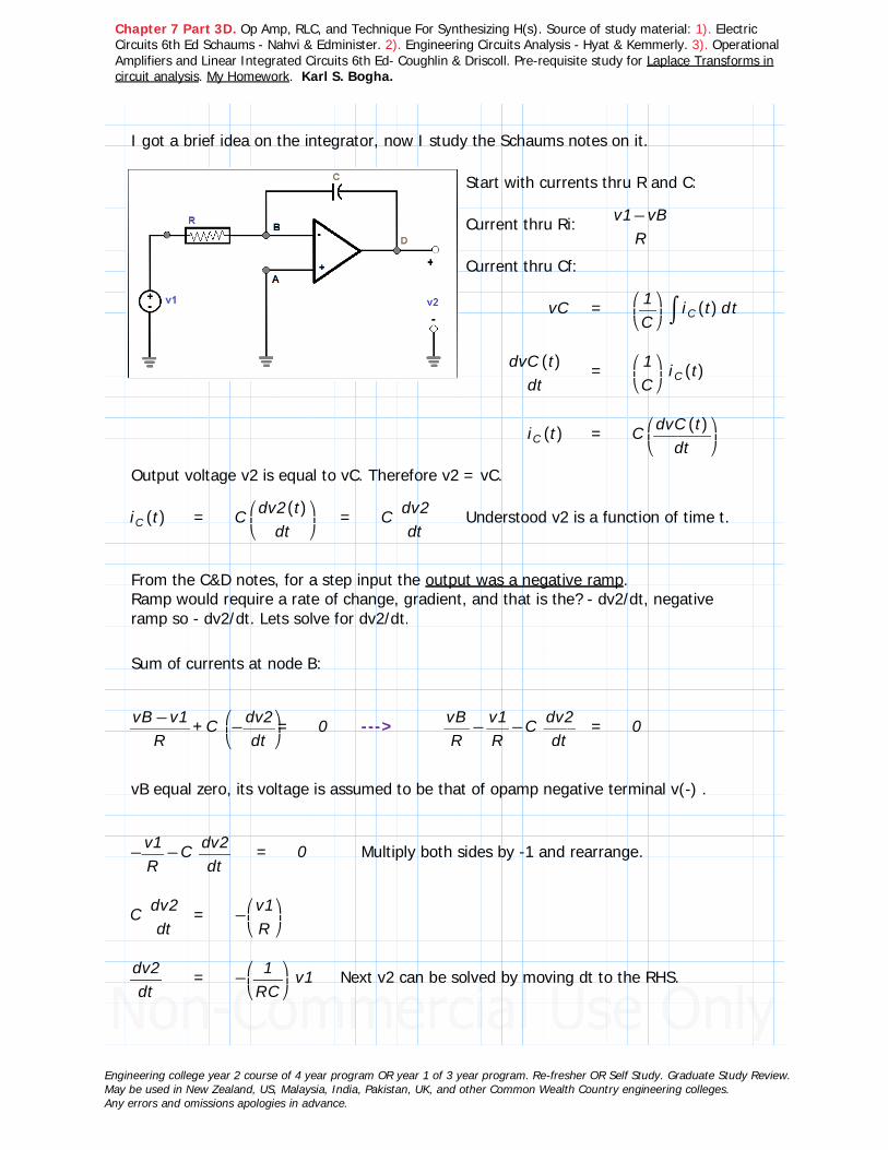
Chapter 7 Part 3D. Op Amp, RLC, and Technique For Synthesizing H(s). Source of study material: 1). Electric Circuits 6th Ed Schaums - Nahvi & Edminister. 2). Engineering Circuits Analysis - Hyat & Kemmerly. 3). Operational Amplifiers and Linear Integrated Circuits 6th Ed- Coughlin & Driscoll. Pre-requisite study for Laplace Transforms in circuit analysis. My Homework. Karl S. Bogha.
I got a brief idea on the integrator, now I study the Schaums notes on it.
Start with currents thru R and C:
Current thru Ri: ―――−v1 vBR
Current thru Cf:
vC = ⎛⎜⎝―1C⎞⎟⎠⌠⌡ diC ((t)) t
―――dvC ((t))
dt= ⎛
⎜⎝―1C⎞⎟⎠
iC ((t))
iC ((t)) = C⎛⎜⎝―――dvC ((t))
dt⎞⎟⎠
Output voltage v2 is equal to vC. Therefore v2 = vC.
iC ((t)) = C⎛⎜⎝―――dv2 ((t))
dt⎞⎟⎠
= C ――dv2dt
Understood v2 is a function of time t.
From the C&D notes, for a step input the output was a negative ramp.Ramp would require a rate of change, gradient, and that is the? - dv2/dt, negative ramp so - dv2/dt. Lets solve for dv2/dt.
Sum of currents at node B:
+―――−vB v1R
C ⎛⎜⎝−――
dv2dt⎞⎟⎠= 0 ---> −−――
vBR
―v1R
C ――dv2dt
= 0
vB equal zero, its voltage is assumed to be that of opamp negative terminal v(-) .
−−―v1R
C ――dv2dt
= 0 Multiply both sides by -1 and rearrange.
C ――dv2dt
= −⎛⎜⎝―v1R⎞⎟⎠
――dv2dt
= −⎛⎜⎝――
1RC⎞⎟⎠
v1 Next v2 can be solved by moving dt to the RHS.
Engineering college year 2 course of 4 year program OR year 1 of 3 year program. Re-fresher OR Self Study. Graduate Study Review.May be used in New Zealand, US, Malaysia, India, Pakistan, UK, and other Common Wealth Country engineering colleges.Any errors and omissions apologies in advance.

Chapter 7 Part 3D. Op Amp, RLC, and Technique For Synthesizing H(s). Source of study material: 1). Electric Circuits 6th Ed Schaums - Nahvi & Edminister. 2). Engineering Circuits Analysis - Hyat & Kemmerly. 3). Operational Amplifiers and Linear Integrated Circuits 6th Ed- Coughlin & Driscoll. Pre-requisite study for Laplace Transforms in circuit analysis. My Homework. Karl S. Bogha.
dv2 = −⎛⎜⎝――
1RC⎞⎟⎠
v1 dt
⌠⌡ ddv2 t = −⌠⎮⌡
d⎛⎜⎝――v1RC⎞⎟⎠
t
v2 = −⎛⎜⎝――
1RC⎞⎟⎠⌠⌡ d((v1)) t Solved, however the intergral limits
can be inserted.Capacitor C was or was not charged before switch t was closed at time t=0? Usual electric circuit - initial condition.This gives a negative infinity for lower limit; it may or may not have been charged for t<0.Upper limit as usual time t where t>0.
v2 = −⎛⎜⎝――
1RC⎞⎟⎠⌠⌡ d−∞
t
((v1)) t
(1/RC) is a multiplier. Because its an opamp, the multiplier here is gain.Agree?
Gain_A = −⎛⎜⎝――
1RC⎞⎟⎠
Agreed.
Now its v2 = A Integral of v1 which would result in v1.
v2 = ⋅A ⌠⌡ d−∞
t
v1 t Schaums notes solves for v2.Elegant!
Example 5.17 Integrator Amplifier.
Let R = 1 kohm. C = 1 uF v1 = sin 2000tAssume v2(0) = 0.
Find v2 (t>0) ?
Solution:
v2 = ⋅−――1
RC⌠⌡ d−∞
t
v1 t = ⋅−――1
RC⌠⌡ d0
t
v1 t
Engineering college year 2 course of 4 year program OR year 1 of 3 year program. Re-fresher OR Self Study. Graduate Study Review.May be used in New Zealand, US, Malaysia, India, Pakistan, UK, and other Common Wealth Country engineering colleges.Any errors and omissions apologies in advance.

Chapter 7 Part 3D. Op Amp, RLC, and Technique For Synthesizing H(s). Source of study material: 1). Electric Circuits 6th Ed Schaums - Nahvi & Edminister. 2). Engineering Circuits Analysis - Hyat & Kemmerly. 3). Operational Amplifiers and Linear Integrated Circuits 6th Ed- Coughlin & Driscoll. Pre-requisite study for Laplace Transforms in circuit analysis. My Homework. Karl S. Bogha.
≔R ⋅1 103 ≔C ⋅1 10−6 =−――1⋅R C
⋅−1 103
⌠⌡ d0
t
v1 t = ⌠⌡ d0
t
sin2000t t = −cos ((2000 t))lim t=t - 0
= −−⎛⎜⎝――
12000
⎞⎟⎠
cos ((2000 t)) ⎛⎜⎝――
12000
⎞⎟⎠
((−cos ((0))))
Multiply in the gain term - 1/RC⋅⋅−1 103 ⎛⎜⎝
−−⎛⎜⎝――
12000
⎞⎟⎠
cos ((2000 t)) ⎛⎜⎝――
12000
⎞⎟⎠
((−cos ((0))))⎞⎟⎠
= ⋅−⎛⎜⎝―12⎞⎟⎠
(( +−cos ((2000 t)) 1))
v2 = 0.5 (( −cos ((2000 t)) 1)) Answer.
C&D Servoamplifier - Example of Integral Amplifier.
A servo amplifier is a circuit whose output is a delayed response to its input. An application may be a ground-following radar signals by a cruise missile or the positioning of an xy table in a manufacturing process. In both applications we may need a circuit that delays the output response due to clutter or noise at the input. C&D chapter 5 page 143.
Example of above circuit from C&D provided in next two figures with notes in them.
Two questions about this circuit's operation were answered.
1. If Ei is in equilibrium, what is Vo in equilibrium ?
2. How long will it take for Vo to change from one equilibrium to another in response to a change in Ei ?
Continued next page.
After that into Section 2.
Engineering college year 2 course of 4 year program OR year 1 of 3 year program. Re-fresher OR Self Study. Graduate Study Review.May be used in New Zealand, US, Malaysia, India, Pakistan, UK, and other Common Wealth Country engineering colleges.Any errors and omissions apologies in advance.


Chapter 7 Part 3D. Op Amp, RLC, and Technique For Synthesizing H(s). Source of study material: 1). Electric Circuits 6th Ed Schaums - Nahvi & Edminister. 2). Engineering Circuits Analysis - Hyat & Kemmerly. 3). Operational Amplifiers and Linear Integrated Circuits 6th Ed- Coughlin & Driscoll. Pre-requisite study for Laplace Transforms in circuit analysis. My Homework. Karl S. Bogha.
Part 3 D: Section 2.
RLC Higher Order Circuits - Continuing Notes With Solved Examples.
Section 2: Operational Amplifier (Op Amp) circuits.
I. Schaums:
11. Integrator and differentiator circuits12. Analog computers13. Low-pass filter14. Decibel (dB)15. Real Op Amp16. A simple Op Amp model 17. Comparator (Briefly)18. Flash analog to digital converter not on notes rather an example related to analog to digital converter was solved in Section 3.
Continuing to Section 3 solving examples, partially solved problems, and supplementary problems.
Apologies for any errors and omissions.
Engineering college year 2 course of 4 year program OR year 1 of 3 year program. Re-fresher OR Self Study. Graduate Study Review.May be used in New Zealand, US, Malaysia, India, Pakistan, UK, and other Common Wealth Country engineering colleges.Any errors and omissions apologies in advance.

Chapter 7 Part D. Op Amp, RLC, and Technique For Synthesizing H(s). Source of study material: 1). Electric Circuits 6th Ed Schaums - Nahvi & Edminister. 2). Engineering Circuits Analysis - Hyat & Kemmerly. 3). Operational Amplifiers and Linear Integrated Circuits 6th Ed- Coughlin & Driscoll. Pre-requisite study for Laplace Transforms in circuit analysis. My Homework. Karl S. Bogha.
Section 2.
Continuation from Section 1. Capacitor and Inductor begin to appear in Opamp circuits.
Section 5.11 Integrator and Differentiator Circuits.
Leaky Integrator.
Circuit below is called a leaky circuit, since the capacitor voltage is continously discharged through the feedback resisitor Rf.
This will result in a reduction in gain |v2/v1| and a phase shift in v2.
From Section 5.13: Schaums: A frequency selective amplifier whose gain decreases from a finite value to zero, as the frequency of the sinusoidal input increases from dc to infinity is called a low pass filter. The plot of gain versus frequency is called a frequency response.
Example 5.18 (Leaky Integrator) :
Given the values of R1, Rf, C, and v1 in the circuit to the right.
Find v2 ?
Solution:
Voltage at v(-) = 0V.AND sum of voltage at node B is 0V. Both do not imply the same meaning. Current is flowing thru node B.
Node B sum of currents: ++――――(( −vB v1))
R1C ⎛⎜⎝――――d (( −vB v2))
dt⎞⎟⎠⎛⎜⎝―――−vB v2
Rf⎞⎟⎠
= 0
Engineering college year 2 course of 4 year program OR year 1 of 3 year program. Re-fresher OR Self Study. Graduate Study Review.May be used in New Zealand, US, Malaysia, India, Pakistan, UK, and other Common Wealth Country engineering colleges.Any errors and omissions apologies in advance.

Chapter 7 Part D. Op Amp, RLC, and Technique For Synthesizing H(s). Source of study material: 1). Electric Circuits 6th Ed Schaums - Nahvi & Edminister. 2). Engineering Circuits Analysis - Hyat & Kemmerly. 3). Operational Amplifiers and Linear Integrated Circuits 6th Ed- Coughlin & Driscoll. Pre-requisite study for Laplace Transforms in circuit analysis. My Homework. Karl S. Bogha.
Voltage at point B = 0V measured to earth.Substitute vB into the expression.vB = 0 −−−――
v1R1
C ――d ((v2))
dt――v2Rf
= 0 Multiply by -1 both sides.
++――v1R1
C ――d ((v2))
dt――v2Rf
= 0
Substitute the values of the components.
++――v1
1000⋅1 10−6
――d ((v2))
dt――
v21000
= 0
Multiply by 1000 to remove the denominator 1000.
++v1 ⋅1 10−3――d ((v2))
dtv2 = 0
Substitute v1 = sin(2000t).
++sin ((2000 t)) ⋅1 10−3――d ((v2))
dtv2 = 0
+⋅1 10−3――d ((v2))
dtv2 = −sin ((2000 t))
The solution for v2 takes the form of the RHS expression with respect to the sinusoid. However, v2 will have an amplitude and phase angle different from v1.
Therefore v2 = ⋅A cos (( +2000 t B)) <--- Solution form should be out of phase, since cos is out of phase with sin, sin(0)=0 and cos(0)=1,cosine makes a sinusoid solution.That's v2 then for that solution's form dv2/dt
can be found from differentiating v2.
――d ((v2))
dt= ⋅−2000 A sin (( +2000 t B))
⋅1 10−3――d ((v2))
dt= ⋅⋅10−3 ((−2000)) A sin (( +2000 t B))
⋅1 10−3――d ((v2))
dt= ⋅−2 A sin (( +2000 t B)) <---
Substitute the above for the expression below:
+⋅1 10−3――d ((v2))
dtv2 = −sin ((2000 t))
Engineering college year 2 course of 4 year program OR year 1 of 3 year program. Re-fresher OR Self Study. Graduate Study Review.May be used in New Zealand, US, Malaysia, India, Pakistan, UK, and other Common Wealth Country engineering colleges.Any errors and omissions apologies in advance.

Chapter 7 Part D. Op Amp, RLC, and Technique For Synthesizing H(s). Source of study material: 1). Electric Circuits 6th Ed Schaums - Nahvi & Edminister. 2). Engineering Circuits Analysis - Hyat & Kemmerly. 3). Operational Amplifiers and Linear Integrated Circuits 6th Ed- Coughlin & Driscoll. Pre-requisite study for Laplace Transforms in circuit analysis. My Homework. Karl S. Bogha.
+⋅−2 A sin (( +2000 t B)) ⋅A cos (( +2000 t B)) = −sin ((2000 t))
Multiply by -1 both sides.Partial solution needs solving for A. As in Schaums.
−⋅2 A sin (( +2000 t B)) ⋅A cos (( +2000 t B)) = sin ((2000 t))
Past this line I had no successThere maybe a trignometry expression for the LHS below that I could not find.That may solve the problem. You can go further to solve it.The next steps provided are from Schaums with the answer.
−⋅2 A sin (( +2000 t B)) ⋅A cos (( +2000 t B)) = ⋅A ‾‾5 sin (( −+2000 t B 26.57 °))
⋅A ‾‾5 sin (( −+2000 t B 26.57 °)) = sin ((2000 t))
Therefore A = ――‾‾5
5= 0.447
B = 26.57 °
v2 = 0.447 cos (( +2000 t 26.57 °)) Answer.
Compare to Example 5.17, where there is no Rf, with the same values for R1 and C, v2 equal:
v2 = 0.5 cos (( −2000 t 1)) Answer for example 5.17.
The amplitude is reduced from 0.5 to 0.447, and there is a change in phase angle from 0 deg to 26.57 degs.
Comments:I was unable to reduce the trignometric expression to the solution. I had a little enough of trig substitutions....... Sorry. I spent some time but did not get close enough.
However I have a proposed solution, which I loosely call by inspection method. Next page. It does get the answer but if you find it not acceptable its understandable. I gave it a try. So please check with your local lecturer/engineer.
You give it a try. If Not Let It Go! For Me It Is Not The First I Missed.Check with your local lecturer, engineer, and math instructor.
Engineering college year 2 course of 4 year program OR year 1 of 3 year program. Re-fresher OR Self Study. Graduate Study Review.May be used in New Zealand, US, Malaysia, India, Pakistan, UK, and other Common Wealth Country engineering colleges.Any errors and omissions apologies in advance.

Chapter 7 Part D. Op Amp, RLC, and Technique For Synthesizing H(s). Source of study material: 1). Electric Circuits 6th Ed Schaums - Nahvi & Edminister. 2). Engineering Circuits Analysis - Hyat & Kemmerly. 3). Operational Amplifiers and Linear Integrated Circuits 6th Ed- Coughlin & Driscoll. Pre-requisite study for Laplace Transforms in circuit analysis. My Homework. Karl S. Bogha.
Let (2000 t + B) = C, substitute for (2000 t + B).And (2000 t ) = C - B = (2000 t + B - B) = 2000 t. Substitute for LHS.
+⋅4 A2 sin2 ((C)) ⋅⋅A2 cos2 ((C)) = ⋅sin2 (( −C B)) <--- Expression.
I can factorise expression into something like below but I did not get far with it.(( −2 A sin Acos)) (( +2 A sin Acos)) = ⋅⋅⋅sin (( −C B)) sin (( −C B))So I continue with the same expression.
+sin2 ((C)) ⋅cos2 ((C)) = 1 <--- This is a trig identity.
+⋅4 A2 sin2 ((C)) ⋅⋅A2 cos2 ((C)) How could my LHS equal the trig identity above?
This got my approach into working it like some 'abstract' solution. Ok its funny.What could A equal to to make the expression equal 1 on the LHS of the trig identity?Is there a Right Angle relationship here (Pythogras)? The Right hand side of the expression is the term sin^2(C-B).
I proceed like this : a2 = 4b2 = 1c2 = =+4 1 5c = ‾‾5
+⋅4 A2 sin2 ((C)) ⋅⋅A2 cos2 ((C)) = 5 = c2
Next I divide by 5 both sides:
+⋅4 ――A2
5sin2 ((C)) ⋅⋅――
A2
5cos2 ((C)) = 1
When I let x = Sqrt(5), then x^2 = 5, my expression now back where it was.
x = ‾‾5 : +⋅4 ―――⎛⎝ ‾‾5⎞⎠
2
5sin2 ((C)) ⋅⋅―――
⎛⎝ ‾‾5⎞⎠2
5cos2 ((C)) = 1
=――‾‾5
2
51 : +4 sin2 ((C)) ⋅cos2 ((C)) = 1 <--- There is also an inverse
trig term Right Angle in character in this expression.So now I let A = x/5 = Sqrt(5)/5. A = =――
‾‾55
0.4472
The angle Theta or B = =asin ((0.4472)) 26.56 degStarted with ---> v2 = ⋅A cos (( +2000 t B)) <--- Solution 'form'...previous pagesSubstitute for A and B:
v2 = ⋅0.4472 cos (( +2000 t 26.56 °)) Answer.Schaums Answer same.
Comments: This is my proposed solution I loosely call it by inspection method.
Engineering college year 2 course of 4 year program OR year 1 of 3 year program. Re-fresher OR Self Study. Graduate Study Review.May be used in New Zealand, US, Malaysia, India, Pakistan, UK, and other Common Wealth Country engineering colleges.Any errors and omissions apologies in advance.
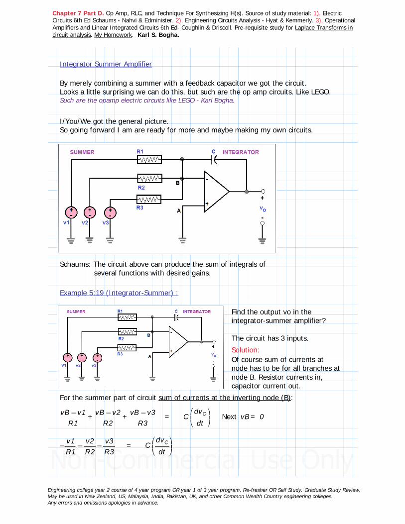
Chapter 7 Part D. Op Amp, RLC, and Technique For Synthesizing H(s). Source of study material: 1). Electric Circuits 6th Ed Schaums - Nahvi & Edminister. 2). Engineering Circuits Analysis - Hyat & Kemmerly. 3). Operational Amplifiers and Linear Integrated Circuits 6th Ed- Coughlin & Driscoll. Pre-requisite study for Laplace Transforms in circuit analysis. My Homework. Karl S. Bogha.
Integrator Summer Amplifier
By merely combining a summer with a feedback capacitor we got the circuit.Looks a little surprising we can do this, but such are the op amp circuits. Like LEGO.Such are the opamp electric circuits like LEGO - Karl Bogha.
I/You/We got the general picture. So going forward I am are ready for more and maybe making my own circuits.
Schaums: The circuit above can produce the sum of integrals of several functions with desired gains.
Example 5:19 (Integrator-Summer) :
Find the output vo in the integrator-summer amplifier?
The circuit has 3 inputs.Solution:Of course sum of currents at node has to be for all branches at node B. Resistor currents in, capacitor current out.
For the summer part of circuit sum of currents at the inverting node (B):
++―――−vB v1
R1―――−vB v2
R2―――−vB v3
R3= C
⎛⎜⎝――dvC
dt⎞⎟⎠
Next vB= 0
−−−――v1R1
――v2R2
――v3R3
= C⎛⎜⎝――dvC
dt⎞⎟⎠
Engineering college year 2 course of 4 year program OR year 1 of 3 year program. Re-fresher OR Self Study. Graduate Study Review.May be used in New Zealand, US, Malaysia, India, Pakistan, UK, and other Common Wealth Country engineering colleges.Any errors and omissions apologies in advance.

Chapter 7 Part D. Op Amp, RLC, and Technique For Synthesizing H(s). Source of study material: 1). Electric Circuits 6th Ed Schaums - Nahvi & Edminister. 2). Engineering Circuits Analysis - Hyat & Kemmerly. 3). Operational Amplifiers and Linear Integrated Circuits 6th Ed- Coughlin & Driscoll. Pre-requisite study for Laplace Transforms in circuit analysis. My Homework. Karl S. Bogha.
vC = vo vo is the voltage vC.
The complete sum of currents at node B (Summer and Integrator) :
−−−――v1R1
――v2R2
――v3R3
= C⎛⎜⎝――dv0
dt⎞⎟⎠
C⎛⎜⎝――dvo
dt⎞⎟⎠
= −−−――v1R1
――v2R2
――v3R3
In the integrator circuit, see figure to the right. Now previous page vo here its v2 :
v2 = v0 = −⎛⎜⎝――
1RC⎞⎟⎠⌠⌡ d−∞
t
v1 t
Similarly here for the integrator summer circuit:
C⎛⎜⎝――dvo
dt⎞⎟⎠
= −⎛⎜⎝++――
v1R1
――v2R2
――v3R3⎞⎟⎠
――dvo
dt= −⎛⎜⎝
++――v1
R1C――
v2R2C
――v3
R3C⎞⎟⎠
vo = −⌠⎮⌡
d
−∝
t
⎛⎜⎝
++――v1
R1C――
v2R2C
――v3
R3C⎞⎟⎠
t Solution. Correct.
Do NOT expand it like the line below thats wrong.
vo = −⎛⎜⎝++――
1R1C
――1
R2C――
1R3C
⎞⎟⎠⌠⌡ d−∝
t
(( ++v1 v2 v3)) t Wrong. I got the picture math wise wrong. Good for one input not for multiple.
Comment:The result above for the integrator has the integral sign, when that expression as a whole is integrated it results with a constant term. What value will it be?Smart thing is... a circuit can be put together to express that constant. The stuff from the First Order Circuits RL and RC. Coming NEXT.
Engineering college year 2 course of 4 year program OR year 1 of 3 year program. Re-fresher OR Self Study. Graduate Study Review.May be used in New Zealand, US, Malaysia, India, Pakistan, UK, and other Common Wealth Country engineering colleges.Any errors and omissions apologies in advance.

Chapter 7 Part D. Op Amp, RLC, and Technique For Synthesizing H(s). Source of study material: 1). Electric Circuits 6th Ed Schaums - Nahvi & Edminister. 2). Engineering Circuits Analysis - Hyat & Kemmerly. 3). Operational Amplifiers and Linear Integrated Circuits 6th Ed- Coughlin & Driscoll. Pre-requisite study for Laplace Transforms in circuit analysis. My Homework. Karl S. Bogha.
Initial condition of Integration.
The initial condition can be accomodated thru a reset switch as shown in the circuit below. This switch works on just the capacitor C.
One of the typical situation, maybe only, on initial conditions is what do we get for voltage or current for time t>0 or shown as t(0+).
Let say we have a switch, we have it closed for t<0, and for this time the capacitor C is charged OR the inductor L is energised. Next at t=0 we open the switch. Next for t>0 the capacitor discharges the current into the circuit starting at t=0, its value would be the fully charged voltage vC at start which is shown here as vo.
Schaums: By momentarily connecting the switch and then disconnecting it at t=t0, an initial value of vo is established across the capacitor and appears at the output v2. For t>t0, the weighted integral of the input is added to the output.
Weighted? If there were more than one input like the summer circuit.
v2 = +−⌠⎮⌡
d
to
t
⎛⎜⎝――
v1R1C
⎞⎟⎠
t vo = +−⎛⎜⎝――
1R1C
⎞⎟⎠⌠⌡ dto
t
v1 t vo vo - here is the initial condition at time t>0.
Engineering college year 2 course of 4 year program OR year 1 of 3 year program. Re-fresher OR Self Study. Graduate Study Review.May be used in New Zealand, US, Malaysia, India, Pakistan, UK, and other Common Wealth Country engineering colleges.Any errors and omissions apologies in advance.

Chapter 7 Part D. Op Amp, RLC, and Technique For Synthesizing H(s). Source of study material: 1). Electric Circuits 6th Ed Schaums - Nahvi & Edminister. 2). Engineering Circuits Analysis - Hyat & Kemmerly. 3). Operational Amplifiers and Linear Integrated Circuits 6th Ed- Coughlin & Driscoll. Pre-requisite study for Laplace Transforms in circuit analysis. My Homework. Karl S. Bogha.
I did the circuit to the left to show for multiple input voltage situation for the summer.
Here vo is the output.
vo = +−⌠⎮⌡
d
to
t
⎛⎜⎝
++――v1
R1C――
v2R2C
――v3
R3C⎞⎟⎠
t vCo
Integrator summer and the initial condition voltage vCo.
Next circuit Differentiator. Done Integrator so maybe there was something missing...a differentiator.
Continued next page.
Engineering college year 2 course of 4 year program OR year 1 of 3 year program. Re-fresher OR Self Study. Graduate Study Review.May be used in New Zealand, US, Malaysia, India, Pakistan, UK, and other Common Wealth Country engineering colleges.Any errors and omissions apologies in advance.

Chapter 7 Part D. Op Amp, RLC, and Technique For Synthesizing H(s). Source of study material: 1). Electric Circuits 6th Ed Schaums - Nahvi & Edminister. 2). Engineering Circuits Analysis - Hyat & Kemmerly. 3). Operational Amplifiers and Linear Integrated Circuits 6th Ed- Coughlin & Driscoll. Pre-requisite study for Laplace Transforms in circuit analysis. My Homework. Karl S. Bogha.
Differentiator:
Swapping an inductor for the capacitor or feedback resistor makes the differentiatior circuit. Same inverting terminal connection.
The output v2 is the derivative of the input signal v1. Do the sum of currents at node B:
−―――−vB v1R
iL = 0 Voltage at vB aproximately zero.iL is negative becuase its leaving the node.
−−―v1R
iL = 0
vL = L⎛⎜⎝――diL
dt⎞⎟⎠
vL = v2
―1L
v2 = ――diL
dtiL = ⎛
⎜⎝―1L⎞⎟⎠⌠⌡ d−∞
t
v2 t
−−―v1R
⎛⎜⎝―1L⎞⎟⎠⌠⌡ d−∞
t
v2 t = 0 ⌠⌡ d−∞
t
v2 t = ⋅−―LR
v1
v2 = ⋅−―LR⎛⎜⎝―v1dt⎞⎟⎠
I have a derivative of the input voltage v1 on the RHS.
Started with saying 'the output v2 is the derivative of the input signal v1'.Thats what I have with the term -(L/R). I have a differentiator. I am saying similarly like the integrator circuit with initial condition, same can be done for differentiator BUT when we differentiate we do not have a constant term! Sorry. So we dont have that circuit. Electrical Engineering Em...Be Math Wise First - Karl Bogha.
Engineering college year 2 course of 4 year program OR year 1 of 3 year program. Re-fresher OR Self Study. Graduate Study Review.May be used in New Zealand, US, Malaysia, India, Pakistan, UK, and other Common Wealth Country engineering colleges.Any errors and omissions apologies in advance.

Chapter 7 Part D. Op Amp, RLC, and Technique For Synthesizing H(s). Source of study material: 1). Electric Circuits 6th Ed Schaums - Nahvi & Edminister. 2). Engineering Circuits Analysis - Hyat & Kemmerly. 3). Operational Amplifiers and Linear Integrated Circuits 6th Ed- Coughlin & Driscoll. Pre-requisite study for Laplace Transforms in circuit analysis. My Homework. Karl S. Bogha.
Section 5.14 Analog Computers (Solving Linear Differential Equations).
How do we solve 'linear differential equations' with opamps?Apply inverting amplifiers, summing and integrator circuits as building blocks to form analog computers for solving linear differential equations. Differentiators I am told are avoided because of considerable noise level. The Lego sort of thing I mentioned in previously.
First rearrange the differential equation so that the highest existing derivative of the desired variable is on one side of the equation. Then add integrators and amplifiers in cascade and in nested loops. Next example demonstrates.
For simplicity we use the notation x' = dx/dt, x'' = dx2/dt2, OR y' = dy/dt, y'' = dy2/dt2.
Example 5.20 (Solving Differential Equation Circuit) :
Design a circuit with x(t) as input to generate output y(t) which satisfies the following equation:
++y'' ((t)) 2 y' ((t)) 3 y ((t)) = x ((t))
Solution:
The circuit above is how we do it. We have THREE opamps. Answer provided first, circuit above, its an example starter circuit for integro-differential circuits. BECAUSE I AM USING INTEGRO AMPLIFIERS INSTEAD OF DIFFERENIAL, THE SOLUTION PROCESS SEEMS LIKE WORKING IN REVERSE!
Engineering college year 2 course of 4 year program OR year 1 of 3 year program. Re-fresher OR Self Study. Graduate Study Review.May be used in New Zealand, US, Malaysia, India, Pakistan, UK, and other Common Wealth Country engineering colleges.Any errors and omissions apologies in advance.

Chapter 7 Part D. Op Amp, RLC, and Technique For Synthesizing H(s). Source of study material: 1). Electric Circuits 6th Ed Schaums - Nahvi & Edminister. 2). Engineering Circuits Analysis - Hyat & Kemmerly. 3). Operational Amplifiers and Linear Integrated Circuits 6th Ed- Coughlin & Driscoll. Pre-requisite study for Laplace Transforms in circuit analysis. My Homework. Karl S. Bogha.
Step 1:++y'' ((t)) 2 y' ((t)) 3 y ((t)) = x ((t)) This is the expression given.
My thinking is like this, 2nd order dervative y'' comes after the first order derivative, so the highest order derivative has to be put at one side, with the intent to reach to the highest order term. We are told to place the highest order to one side.
y'' ((t)) = −−x ((t)) 2 y' ((t)) 3 y ((t))y'' = −−x 2 y' 3 y Taking the (t) out to make it
more readable for the circuit.
There are the three input circuit above to left into opamp #1; x, -2y', and -3y. I have to work thru circuit to sort the 3 inputs x(t) - 2y'(t) - 3y(t).
Step 2:Instead of doing the differentiation on something, we are advised to intergrate.Integrating y'' results in dropping back to the first derivative y'.
y'' = −−x 2 y' 3 y <---= −−x 3 y 2 y' <--- arranged in increasing order
Use the summer integrator for opamp 1 to integrate the expression above.Apply summer integrator expression to solve for R1, R2, R3, and C1.
v1 = −⌠⎮⌡
d
to
t
⎛⎜⎝
++――vx
R1C1――
v3yR2C1
――v2y'
R3C1⎞⎟⎠
t <--- We are integrating the y'' expression which results in ? y'. I show the voltages as vx, v3y, and v2y' for each branch OR v1, v2, and v3.
Engineering college year 2 course of 4 year program OR year 1 of 3 year program. Re-fresher OR Self Study. Graduate Study Review.May be used in New Zealand, US, Malaysia, India, Pakistan, UK, and other Common Wealth Country engineering colleges.Any errors and omissions apologies in advance.
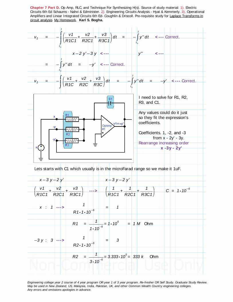
Chapter 7 Part D. Op Amp, RLC, and Technique For Synthesizing H(s). Source of study material: 1). Electric Circuits 6th Ed Schaums - Nahvi & Edminister. 2). Engineering Circuits Analysis - Hyat & Kemmerly. 3). Operational Amplifiers and Linear Integrated Circuits 6th Ed- Coughlin & Driscoll. Pre-requisite study for Laplace Transforms in circuit analysis. My Homework. Karl S. Bogha.
v1 = −⌠⎮⌡
d
to
t
⎛⎜⎝
++――v1
R1C1――
v2R2C1
――v3
R3C1⎞⎟⎠
t = −⌠⌡ dto
t
y'' t <--- Correct.
−−x 2 y' 3 y <--- y'' <---
= −⌠⌡ dto
t
y'' t = −y' <--- Correct.
v1 = −⌠⎮⌡
d⎛⎜⎝
++――v1
R1C――
v2R2C
――v3
R3C⎞⎟⎠
t = −⌠⌡ dto
t
y'' t = −y' <--- Correct.
I need to solve for R1, R2, R3, and C1.
Any values could do it just so they fit the expression's coefficients.
Coefficients. 1, -2, and -3 from x - 2y' - 3y.Rearrange increasing order x -3y - 2y'
Lets starts with C1 which usually is in the microFarad range so we make it 1uF.
−−x 3 y 2 y' −−x 3 y 2 y'
⎛⎜⎝
++――v1
R1C1――
v2R2C1
――v3
R3C1⎞⎟⎠
---> ⎛⎜⎝
++――1
R1C1――
1R2C1
――1
R3C1⎞⎟⎠
C = ⋅1 10−6
x : 1 ---> ――――1
⋅⋅R1 1 10−6= 1
R1 = =―――1
⋅1 10−6⋅1 106 = 1 M Ohm
−3 y : 3 ---> ――――1
⋅⋅R2 1 10−6= 3
R2 = =―――1
⋅3 10−6⋅3.333 105 = 333 k Ohm
Engineering college year 2 course of 4 year program OR year 1 of 3 year program. Re-fresher OR Self Study. Graduate Study Review.May be used in New Zealand, US, Malaysia, India, Pakistan, UK, and other Common Wealth Country engineering colleges.Any errors and omissions apologies in advance.

Chapter 7 Part D. Op Amp, RLC, and Technique For Synthesizing H(s). Source of study material: 1). Electric Circuits 6th Ed Schaums - Nahvi & Edminister. 2). Engineering Circuits Analysis - Hyat & Kemmerly. 3). Operational Amplifiers and Linear Integrated Circuits 6th Ed- Coughlin & Driscoll. Pre-requisite study for Laplace Transforms in circuit analysis. My Homework. Karl S. Bogha.
−2 y' : 2 ---> ――――1
⋅⋅R3 1 10−6= 2
R3 = =―――1
⋅2 10−6⋅5 105 = 500 k Ohm
Recap: C1 = 1 uF
R1 = 1 M
R2 = 333 k
R3 = 500 k
Almost getting the 1st opamp completed.
Opamp #1 three resistor make up the summer circuit, the capacitor C1 makes up the integrator. Being an integrator circuit, we go from higher y'' to lower order y'.The expression y'' = x - 3y - 2y'. These terms in expression x - 3y -2y' are what we want to get solved. The LHS term y'' we dont need to work on so long we understand that it is the 2nd derivative y''.
Now it looks like y'' is the input, loosely speaking, to opamp #1. With y'' the input the outcome of the integrator for opamp #1 will be y'. Since its an inverting opamp its negative y', (-y'). Correct.
We got the values of the resistors and capacitor solved, thru the coefficients of the terms in y''.
For the inputs of opamp #1 we got solved were x(t), and -2y'(t) ie x - 2y'.I have not solved the y term, ie -3y. This comes from opamp #2.
Input of opamp #2 ? -y'. Correct.
Continued next page.
Engineering college year 2 course of 4 year program OR year 1 of 3 year program. Re-fresher OR Self Study. Graduate Study Review.May be used in New Zealand, US, Malaysia, India, Pakistan, UK, and other Common Wealth Country engineering colleges.Any errors and omissions apologies in advance.

Chapter 7 Part D. Op Amp, RLC, and Technique For Synthesizing H(s). Source of study material: 1). Electric Circuits 6th Ed Schaums - Nahvi & Edminister. 2). Engineering Circuits Analysis - Hyat & Kemmerly. 3). Operational Amplifiers and Linear Integrated Circuits 6th Ed- Coughlin & Driscoll. Pre-requisite study for Laplace Transforms in circuit analysis. My Homework. Karl S. Bogha.
Step 3:Opamp#1 send a signal -y' into opamp number 2.We want out of opamp number 2's output the value of y.Opamp #2 is non inverting. We want a gain of 1, or more precisely -1.We need to fix the values of R4 and C2 to get a gain of 1.
v2 = −⌠⎮⌡
d⎛⎜⎝――
v1R4C2
⎞⎟⎠
t = −⎛⎜⎝――
1R4C2
⎞⎟⎠⌠⌡ d((v1)) t = −⌠⌡ d((−y')) t = y
Again set C2 = 1uF.
gain : 1 ---> ――――1
⋅⋅R4 1 10−6= 1
R4 = =―――1
⋅1 10−6⋅1 106 = 1 M Ohm
Shown above the outcome of opamp #2 is y. However, I need -y for the input in opamp #1. So I have one more opamp #3 to go thru to change the value back to -y. Here I do NOT need an integrator circuit, just an inverting circuit with a gain of 1. For which a 10kohm Ri and 10kohm Rf is needed. As shown in the circuit layout next.
gain_A_opamp#3 = ―v3
v2= −―
RiRf
= =−―――⋅10 103
⋅10 103−1
v3 = ⋅−1 v2 v2 we know is equal to y.= −v2
v3 = −((y)) Connect this output to the input of opamp #1 for -y.
Engineering college year 2 course of 4 year program OR year 1 of 3 year program. Re-fresher OR Self Study. Graduate Study Review.May be used in New Zealand, US, Malaysia, India, Pakistan, UK, and other Common Wealth Country engineering colleges.Any errors and omissions apologies in advance.

Chapter 7 Part D. Op Amp, RLC, and Technique For Synthesizing H(s). Source of study material: 1). Electric Circuits 6th Ed Schaums - Nahvi & Edminister. 2). Engineering Circuits Analysis - Hyat & Kemmerly. 3). Operational Amplifiers and Linear Integrated Circuits 6th Ed- Coughlin & Driscoll. Pre-requisite study for Laplace Transforms in circuit analysis. My Homework. Karl S. Bogha.
The solution for the circuit shown above.
Step 4:
Crcuit above shows supply inputs to opamp #1.- Connect or feed v1 = -y' into R3 ie the input of opamp #1.- Connect v2 = y to the unity gain inverting opamp #3 to generate -y, which is then connected or feed to R2 the input of opamp #1. - Connect or feed the voltage source x(t) to R1 the input of opamp #1. The 4 steps showed the solution and the circuit shown above.
Voltages as x, -3y, and -2y' for each branch entering the node before opamp 1 input terminals are shown in the figure to the right --->
Next example continued next page.
Engineering college year 2 course of 4 year program OR year 1 of 3 year program. Re-fresher OR Self Study. Graduate Study Review.May be used in New Zealand, US, Malaysia, India, Pakistan, UK, and other Common Wealth Country engineering colleges.Any errors and omissions apologies in advance.

Chapter 7 Part D. Op Amp, RLC, and Technique For Synthesizing H(s). Source of study material: 1). Electric Circuits 6th Ed Schaums - Nahvi & Edminister. 2). Engineering Circuits Analysis - Hyat & Kemmerly. 3). Operational Amplifiers and Linear Integrated Circuits 6th Ed- Coughlin & Driscoll. Pre-requisite study for Laplace Transforms in circuit analysis. My Homework. Karl S. Bogha.
Example 5.21 (Differential Equation Circuit) :
Design an opamp circuit as an ideal voltage source v(t) satisfying the equation v' + v = 0 for t>0, with v(0) = 1V.
Solution:+v' v = 0
+――dv ((t))
dtv ((t)) = 0
Place the higher order term to one side, to the left.
v' = −v Intepret like this, integrate v' we get v, and remember the negative unity gain, that makes it -v.
v ((0)) = 0Solution is for t>0, NOT t=0 and t>0, rather t>0.
⌠⌡ dv' t = v = −v Next the inverting opamp gives the negative gain. Therefore v becomes -v.
<--- Solution for circuitwith integrator andinitial condition voltage with switch.
Before the switch is opened, t<0 there is a voltage source of 1V.
This voltage source is across the capacitor, and is the voltage at the output terminal of the opamp.
When the switch is opened at t=0, the voltage that appears at the opamp output is the discharging capacitor voltage.
Engineering college year 2 course of 4 year program OR year 1 of 3 year program. Re-fresher OR Self Study. Graduate Study Review.May be used in New Zealand, US, Malaysia, India, Pakistan, UK, and other Common Wealth Country engineering colleges.Any errors and omissions apologies in advance.

Chapter 7 Part D. Op Amp, RLC, and Technique For Synthesizing H(s). Source of study material: 1). Electric Circuits 6th Ed Schaums - Nahvi & Edminister. 2). Engineering Circuits Analysis - Hyat & Kemmerly. 3). Operational Amplifiers and Linear Integrated Circuits 6th Ed- Coughlin & Driscoll. Pre-requisite study for Laplace Transforms in circuit analysis. My Homework. Karl S. Bogha.
Before the switch was opened t<0.
Fix the values of R and C.
Lets make C=1uF.
≔C ⋅1 10−6 = 1 uF
v' = −v
The input voltage to the opamp must be v and the output voltage -v. Gain -1.
≔R =―――1
⋅1 10−6⋅1 106
R = 1 M ohm
Next the switch is opened t>0.
The voltage decreases exponentially from 1V to 0V at vo.
Series RC circuit time constant: ≔τ =⋅R C 1
vo ((t)) = −1 e――−1 tτ V
vo (( >t 0)) = −1 e−t = −e−t V Answer.
Comments:Required a look up on First Order RLC circuits!I needed to apply the steps of the previous example.Because I am working with integrator opamp I need to do a little reverse on it NOT straight differentiate. Key step for me was higher order term to one side, then work like integrating.
Topics coming next are low pass filter, decibles dB, real opamps, simple opamp model, comparator, and analog to digital converter. I briefly go over low pass filter and decibles here in their introductory circuits. They are primarily found in Frequency Response and Filter chapters.Most these topics are short or brief here in Schaums and are really indepth in other circuits chapters. Just so I/You/We see these can be found in opamps circuits.
Engineering college year 2 course of 4 year program OR year 1 of 3 year program. Re-fresher OR Self Study. Graduate Study Review.May be used in New Zealand, US, Malaysia, India, Pakistan, UK, and other Common Wealth Country engineering colleges.Any errors and omissions apologies in advance.

Chapter 7 Part D. Op Amp, RLC, and Technique For Synthesizing H(s). Source of study material: 1). Electric Circuits 6th Ed Schaums - Nahvi & Edminister. 2). Engineering Circuits Analysis - Hyat & Kemmerly. 3). Operational Amplifiers and Linear Integrated Circuits 6th Ed- Coughlin & Driscoll. Pre-requisite study for Laplace Transforms in circuit analysis. My Homework. Karl S. Bogha.
Skip/Bypass Section 5.13 Low-Pass Filter.
This section is very brief and the subject matter is extensive to cover in a paragraph comes with one Example 5.22. This can be covered in circuits studies in other chapters or filters. Not really needed here.
See next page for some background material on the dB.
Section 5.14 Decibel dB.
Gain of the opamp is expressed on a logarithmic scale.The unit is called the decibel (dB).
Gain in dB = ⋅20 log10 ((gain)) <--- with the 20 included
gain =|||―v2
v1
|||
v2 the output andv1 the input voltage.
Entering log in Mathcad: log (###, [base])Example log of 1000 to base 10: log(1000, [10])
=log (( ,1000 10[[ ]])) 3[[ ]] Returns answer in square bracket.
Example: A gain of 1000, the gain in dB?
Gain in dB = =⋅20 log (( ,1000 10[[ ]])) 60[[ ]]
Gain in dB = 60 dB.
What is the -3dB attenuation ?
Most heard in sound/acoustics engineering. Attenuation is opposite of amplification, where attenuation is the reduction of the signal, made smaller in amplitude.An attenuation of -3dB corresponds to gain v2/v1 = 1 / (SQRT(2)),which for simplicity is 20 times log 0.7071 to base 10 = -3.0 dB.
Gain―v2v1
= =――1
‾‾20.7071
-3 dB = =⋅20 log (( ,0.7071 10[[ ]])) −3.0104[[ ]] <--- -3dB, the negative sign -3.0 < 1.0 its attenuation.
Where did the 20 times log 0.7071 to base 10 come from? See next page.
Engineering college year 2 course of 4 year program OR year 1 of 3 year program. Re-fresher OR Self Study. Graduate Study Review.May be used in New Zealand, US, Malaysia, India, Pakistan, UK, and other Common Wealth Country engineering colleges.Any errors and omissions apologies in advance.

Chapter 7 Part D. Op Amp, RLC, and Technique For Synthesizing H(s). Source of study material: 1). Electric Circuits 6th Ed Schaums - Nahvi & Edminister. 2). Engineering Circuits Analysis - Hyat & Kemmerly. 3). Operational Amplifiers and Linear Integrated Circuits 6th Ed- Coughlin & Driscoll. Pre-requisite study for Laplace Transforms in circuit analysis. My Homework. Karl S. Bogha.
The origin on the previous page -3dB can be found in the Filter chapter of the circuits textbook, OR similar subject matter. I got this material, presented on this page, from: U of California at San Diego on the internet. 'A Practical Guide to Decibels. A Companion to The Art of Electronics Student Manual Lab 2'. UCSD Physics 120A. David Kleinfeld and Han Lin. Its a simple explanation made it worthwhile for me.
Power Ratios: Attenuator 1/2.
=⋅10 log ⎛⎜⎝,―
12
10[[ ]]⎞⎟⎠−3.0103[[ ]]
Power Ratios: Amplifier 2X.
=⋅10 log (( ,2 10[[ ]])) 3.0103[[ ]]
Voltage Ratios: Attenuator. =⋅20 log ⎛⎜⎝
,――1
‾‾210[[ ]]⎞⎟⎠−3.0103[[ ]]
Engineering college year 2 course of 4 year program OR year 1 of 3 year program. Re-fresher OR Self Study. Graduate Study Review.May be used in New Zealand, US, Malaysia, India, Pakistan, UK, and other Common Wealth Country engineering colleges.Any errors and omissions apologies in advance.

Chapter 7 Part D. Op Amp, RLC, and Technique For Synthesizing H(s). Source of study material: 1). Electric Circuits 6th Ed Schaums - Nahvi & Edminister. 2). Engineering Circuits Analysis - Hyat & Kemmerly. 3). Operational Amplifiers and Linear Integrated Circuits 6th Ed- Coughlin & Driscoll. Pre-requisite study for Laplace Transforms in circuit analysis. My Homework. Karl S. Bogha.
Whats the purpose of this ?Seems something large can be scaled down by the base of the log.Much more can be placed in a graph when the x-axis is in log frequency and the gain on the y-axis is in dB (20 x log ### to base 10) also in log.Which the x-axis is frequency and we know thats huge in kilo or mega Hertz.We have both in log scale. dB (20 x log ### to base 10) Vs log frequency to base 10 - For the Voltage Gain.
These kinds of plots are called Bode Plots.Usually for plotting the frequency response of amplifiers and filters.Takes a study on Bode Plots NOT merely a graph its a science of its own.
There is an example here but it assumes some simple filter studying completed, short example, knowing very well its a separate topic of this chapter. So I skip it for Section 5.16.There is a formula-expression that is explained in a later chapter.
Section 5.15 Real Op AmpsI remember this back in college days that there was the ideal condition for the equations and adjustments to be made for the real conditions. The reason we continue with ideal conditions because the equations are more manageable - I like it simple.Karl Bogha: In the circuit problems we went thru, we assumed these were real conditions. The reasoning mostly was in the circuit analysis and design side of things. The opamp has internal or external restrictions or flaws, from the ideal conditions. So here we just want to take into consideration their impact if and when applicable. Thats All I am prepared to go. Lets hope it isnt much different from what I said.
Circuit with an inverting opamp, has a feedback resistor. Closed Loop Gain. - Acl.
Engineering college year 2 course of 4 year program OR year 1 of 3 year program. Re-fresher OR Self Study. Graduate Study Review.May be used in New Zealand, US, Malaysia, India, Pakistan, UK, and other Common Wealth Country engineering colleges.Any errors and omissions apologies in advance.

Chapter 7 Part D. Op Amp, RLC, and Technique For Synthesizing H(s). Source of study material: 1). Electric Circuits 6th Ed Schaums - Nahvi & Edminister. 2). Engineering Circuits Analysis - Hyat & Kemmerly. 3). Operational Amplifiers and Linear Integrated Circuits 6th Ed- Coughlin & Driscoll. Pre-requisite study for Laplace Transforms in circuit analysis. My Homework. Karl S. Bogha.
The assumptions for ideal opamps we made early provided here:
1. Opamp pulls no current. Why? Input Resistance equals infinity.2. Opamp performance is not impacted or influenced by the load because the Output Resistance equals zero.3. Opamp's open loop gain is infinite at all frequencies (A = Infinite (Huge)). Open loop gain does not have a feedback connection - Thats All.
Now how do the real opamps differ from the above rather valid assumptions?
1. Opamp pulls current. Its not really infinite the input resistance, its large, but that does not mean no current is pulled by the opamp. 2. The load impacts/affects the gain. Because there is some resistance at the opamp output, Output Resistance is greater than zero.3. Open loop gain is NOT infinite. It decreases with frequency.
Basically the conditions for ideal were brought into physical real situation.Adjustments can be made. For low frequencies the opamp actual performance does not deviate from the ideal-model assumptions.The next 2 examples serve to show the effect of the 3 real opamps conditions ie, the finite input resistance, non-zero output resistance, and finite gain.
Example 5.24 (Real Opamps) :For the inverting opamp circuit below, assume Ri = Infinity, Ro = 0, and real valued gain A. Develop an expression for v2/v1 in terms of k =R2/R1 and A.
Ri and Ro areshown internal to the opamp. R1 the input resistance, and R2 the feedback resistance, with RL the load.
Engineering college year 2 course of 4 year program OR year 1 of 3 year program. Re-fresher OR Self Study. Graduate Study Review.May be used in New Zealand, US, Malaysia, India, Pakistan, UK, and other Common Wealth Country engineering colleges.Any errors and omissions apologies in advance.

Chapter 7 Part D. Op Amp, RLC, and Technique For Synthesizing H(s). Source of study material: 1). Electric Circuits 6th Ed Schaums - Nahvi & Edminister. 2). Engineering Circuits Analysis - Hyat & Kemmerly. 3). Operational Amplifiers and Linear Integrated Circuits 6th Ed- Coughlin & Driscoll. Pre-requisite study for Laplace Transforms in circuit analysis. My Homework. Karl S. Bogha.
Solution:
The opamp real condition input voltage, output voltage, and gain are shown coloured in.
With the input resistance finite NOT infinity, current is pulled in by the opamp so there is voltage across its terminals vd. The output voltage being v2, the source input voltage v1, and gain A.
Apply sum of currents equal zero at node B:
+―――−vB v1
R1―――−vB v2
R2= 0
vB = −vd Opamp circuit shows the terminal -ve is connected to B, hence the voltage is -vd.
+――――−((−vd)) v1
R1――――
−((−vd)) v2R2
= 0
+―――−−vd v1
R1―――
−−vd v2R2
= 0
How do I bring in A in this expression, we have v1 and v2 ? What the engineers did.Which v1 is external to the opamp is here equal to vd in the real opamp. R1 resistance is very high no current flow, so the voltage at end of R1 terminal is v1. Now vd = v1.
vd = A (( −−+v ' v ')) = Avd
vd = A (( −−+v ' v ')) = Av1
―v2v1
= A Substitute for vd A = ―v2vd
Therefore vd = ―v2A
Engineering college year 2 course of 4 year program OR year 1 of 3 year program. Re-fresher OR Self Study. Graduate Study Review.May be used in New Zealand, US, Malaysia, India, Pakistan, UK, and other Common Wealth Country engineering colleges.Any errors and omissions apologies in advance.

Chapter 7 Part D. Op Amp, RLC, and Technique For Synthesizing H(s). Source of study material: 1). Electric Circuits 6th Ed Schaums - Nahvi & Edminister. 2). Engineering Circuits Analysis - Hyat & Kemmerly. 3). Operational Amplifiers and Linear Integrated Circuits 6th Ed- Coughlin & Driscoll. Pre-requisite study for Laplace Transforms in circuit analysis. My Homework. Karl S. Bogha.
+―――−−vd v1
R1―――
−−vd v2R2
= −−−−――v1R1
――vdR1
――v2R2
――vdR2
= 0
−−−−――v1R1
――v2⋅A R1
――v2R2
――v2⋅A R2
= −−−――v1R1
―1A⎛⎜⎝
+――v2R1
――v2R2⎞⎟⎠――v2R2
= 0
−v2 ⎛⎜⎝+―
1A⎛⎜⎝
+――1
R1――
1R2⎞⎟⎠――
1R2⎞⎟⎠
= ――v1R1
−R1 ⎛⎜⎝+―
1A⎛⎜⎝
+――1
R1――
1R2⎞⎟⎠――
1R2⎞⎟⎠
= ―v1v2
Multiply by -1 both sides
⎛⎜⎝
+――R1A⎛⎜⎝
+――1
R1――
1R2⎞⎟⎠――R1R2⎞⎟⎠
= −―v1v2
⎛⎜⎝
+――R1A⎛⎜⎝―――
+R2 R1R1R2
⎞⎟⎠――R1R2⎞⎟⎠
= +⎛⎜⎝――――
+R1R2 R12
AR1R2
⎞⎟⎠――R1R2
= −―v1v2
+⎛⎜⎝――――
+R1R2 R12
AR1R2
⎞⎟⎠――R1R2
= −―v1v2
―――――――++R1R2 R12 AR12
AR1R2= ―――――――
+R1R2 R12 (( +1 A))AR1R2
= −―v1v2
Next invert the expression.
−―v2v1
= ―――――――AR1R2
−R1R2 R12 (( +1 A))Divide top and bottom LHS by R1^2
−―v2v1
= ―――――A ――R2
R1
+――R2R1
⋅1 (( +1 A))= ―――
A k++k 1 A
= ―――kA
++A k 1
Multiply by -1 both sides
―v2v1
= ―――−kA
++A k 1Answer.
When A>>k the ratio v2/v1 is reduced to approximately -k. Where A/(A+1) cancels off.
When A>>k : ―v2v1
= −k Answer.
Following Example 5.25 was similar to 5.24. However I could not get the same solution as Schaum's. Schaum's solution maybe wrong maybe right. Next.
Engineering college year 2 course of 4 year program OR year 1 of 3 year program. Re-fresher OR Self Study. Graduate Study Review.May be used in New Zealand, US, Malaysia, India, Pakistan, UK, and other Common Wealth Country engineering colleges.Any errors and omissions apologies in advance.

Chapter 7 Part D. Op Amp, RLC, and Technique For Synthesizing H(s). Source of study material: 1). Electric Circuits 6th Ed Schaums - Nahvi & Edminister. 2). Engineering Circuits Analysis - Hyat & Kemmerly. 3). Operational Amplifiers and Linear Integrated Circuits 6th Ed- Coughlin & Driscoll. Pre-requisite study for Laplace Transforms in circuit analysis. My Homework. Karl S. Bogha.
Example 5.25 (Real Opamps) :
Develop an expression for v2/v1, in the amplifier circuit provided below, in terms of circuit elements k = R2/R1. (Actually 3 of ' - ' the dash character weresigns are shown in parallel thats meaning approximately equal or equivalent i could only show 2 here k = R2/R1. The gain A of the op amp is a real valued number.
Solution:
As usual, ......I do the sum of currents, at node B:
-vd, -ve because the opamp terminal connection given is a negative at B. Hence -vd.
++――――(( −vB v1))
R1―vd
Ri⎛⎜⎝―――−vB v2
R2⎞⎟⎠
= 0 vB = −vd
++――――⎛⎝ −−vd v1⎞⎠
R1――−vd
Ri⎛⎜⎝―――
−−vd v2R2
⎞⎟⎠
= −−−−−――vdR1
――v1R1
―vd
Ri――vd
R2――v2R2
= 0
Engineering college year 2 course of 4 year program OR year 1 of 3 year program. Re-fresher OR Self Study. Graduate Study Review.May be used in New Zealand, US, Malaysia, India, Pakistan, UK, and other Common Wealth Country engineering colleges.Any errors and omissions apologies in advance.

Chapter 7 Part D. Op Amp, RLC, and Technique For Synthesizing H(s). Source of study material: 1). Electric Circuits 6th Ed Schaums - Nahvi & Edminister. 2). Engineering Circuits Analysis - Hyat & Kemmerly. 3). Operational Amplifiers and Linear Integrated Circuits 6th Ed- Coughlin & Driscoll. Pre-requisite study for Laplace Transforms in circuit analysis. My Homework. Karl S. Bogha.
++++――vdR1
――v1R1
―vd
Ri――vd
R2――v2R2
= 0 Multiply by -1 both sides, makes a positive equation.
From previous example:
A = ―v2vd
Therefore v2 = Avd
See circuit to the left.Ro and RL are in series.With a voltage v2 = Avd
v2 is the voltage across RL, which is also the voltage at opamp output terminal.
Applying voltage division for Ro and RL, with Ro being internal to the opamp while RL external to the opamp.
v2 = ⎛⎜⎝―――
RL+Ro RL
⎞⎟⎠
Avd Some difference compared to previous example. Here we solve for vd but with the resistors RL and Ro included.
vd = v2⎛⎜⎝―――
+Ro RL⋅A RL
⎞⎟⎠
Substitute vd in this expression.Not easy for me! I can say I will not have the same result as the Engineers.
++++――vdR1
――v1R1
―vd
Ri――vd
R2――v2R2
= 0
++++―――――v2⎛⎜⎝―――
+Ro RL⋅A RL
⎞⎟⎠
R1――v1R1
―――――v2⎛⎜⎝―――
+Ro RL⋅A RL
⎞⎟⎠
Ri―――――v2⎛⎜⎝―――
+Ro RL⋅A RL
⎞⎟⎠
R2――v2R2
= 0
++⋅⋅v2⎛⎜⎝―――
+Ro RL⋅A RL
⎞⎟⎠⎛⎜⎝
++――1
R1―1
Ri――
1R2⎞⎟⎠――v1R1
――v2R2
= 0
+――v1R1
⋅v2⎛⎜⎝
⋅⎛⎜⎝―――
+Ro RL⋅A RL
⎞⎟⎠⎛⎜⎝
+++――1
R1―
1Ri
――1
R2――
1R2⎞⎟⎠⎞⎟⎠
= 0
+――v1R1
⋅v2⎛⎜⎝
⋅⎛⎜⎝―――
+Ro RL⋅A RL
⎞⎟⎠⎛⎜⎝
++――1
R1―
1Ri
――2
R2⎞⎟⎠⎞⎟⎠
= 0
Engineering college year 2 course of 4 year program OR year 1 of 3 year program. Re-fresher OR Self Study. Graduate Study Review.May be used in New Zealand, US, Malaysia, India, Pakistan, UK, and other Common Wealth Country engineering colleges.Any errors and omissions apologies in advance.

Chapter 7 Part D. Op Amp, RLC, and Technique For Synthesizing H(s). Source of study material: 1). Electric Circuits 6th Ed Schaums - Nahvi & Edminister. 2). Engineering Circuits Analysis - Hyat & Kemmerly. 3). Operational Amplifiers and Linear Integrated Circuits 6th Ed- Coughlin & Driscoll. Pre-requisite study for Laplace Transforms in circuit analysis. My Homework. Karl S. Bogha.
⋅v2⎛⎜⎝
⋅⎛⎜⎝―――
+Ro RL⋅A RL
⎞⎟⎠⎛⎜⎝
++――1
R1―
1Ri
――2
R2⎞⎟⎠⎞⎟⎠
= −――v1R1
⋅⋅⋅((R1)) ⎛⎜⎝―1A⎞⎟⎠⎛⎜⎝―――
+Ro RLRL
⎞⎟⎠⎛⎜⎝
++――1
R1―1
Ri――
2R2⎞⎟⎠
= −―v1v2
⋅⋅⎛⎜⎝――R1A⎞⎟⎠⎛⎜⎝―――
+Ro RLRL
⎞⎟⎠⎛⎜⎝
++――1
R1―1
Ri――
2R2⎞⎟⎠
= −⎛⎜⎝―v1v2⎞⎟⎠
⋅⎛⎜⎝―1A⎞⎟⎠⎛⎜⎝―――
+Ro RLRL
⎞⎟⎠⎛⎜⎝
++――1
R1―1
Ri――
2R2⎞⎟⎠
= −⎛⎜⎝―v1v2⎞⎟⎠⎛⎜⎝――
1R1⎞⎟⎠
Multiply by R2
⋅⎛⎜⎝―1A⎞⎟⎠⎛⎜⎝―――
+Ro RLRL
⎞⎟⎠⎛⎜⎝
++――R2R1
――R2Ri
――2 R2
R2⎞⎟⎠
= −⎛⎜⎝―v1v2⎞⎟⎠⎛⎜⎝――R2R1⎞⎟⎠
⋅⋅⎛⎜⎝―v2v1⎞⎟⎠⎛⎜⎝―1A⎞⎟⎠⎛⎜⎝―――
+Ro RLRL
⎞⎟⎠⎛⎜⎝
++――R2R1
――R2Ri
――2 R2
R2⎞⎟⎠
= −⎛⎜⎝――R2R1⎞⎟⎠
= −k R2/R1 = k
⎛⎜⎝―v2v1⎞⎟⎠
= ――――――――――−k
⋅⎛⎜⎝―1A⎞⎟⎠⎛⎜⎝―――
+Ro RLRL
⎞⎟⎠⎛⎜⎝
++k ――R2Ri
2⎞⎟⎠
My Answer.
In the real opamp there is some resistance Ro but it is yet much lower compared to RL. This can allow me to make the 2nd term in the RHS denominator equal 1.
Ro = 0.0001 to 1
⎛⎜⎝―――
+Ro RLRL
⎞⎟⎠
= ⎛⎜⎝―――
+1 RLRL
⎞⎟⎠
~ ⎛⎜⎝――RLRL⎞⎟⎠
~ 1
⎛⎜⎝―v2v1⎞⎟⎠
= ――――――−k
⋅⎛⎜⎝―1A⎞⎟⎠⎛⎜⎝
++k ――R2Ri
2⎞⎟⎠
= ―――――――−k
++―kA⎛⎜⎝―1A⎞⎟⎠⎛⎜⎝――R2Ri
⎞⎟⎠―2A
My Answer.
Now I have the RHS bottom term: ⎛⎜⎝―1A⎞⎟⎠⎛⎜⎝
++k ――R2Ri
2⎞⎟⎠= ++―
kA―1A⎛⎜⎝――R2Ri
⎞⎟⎠―2A
Now I simplify the 2 term in the RHS.
Ri, input resistance, is much larger than R2. R2/Ri results in a large number as large as A if A were to equal 10^6 or 100k.
Then the 2nd term cancels off (1/A)(A) = 1.
Engineering college year 2 course of 4 year program OR year 1 of 3 year program. Re-fresher OR Self Study. Graduate Study Review.May be used in New Zealand, US, Malaysia, India, Pakistan, UK, and other Common Wealth Country engineering colleges.Any errors and omissions apologies in advance.
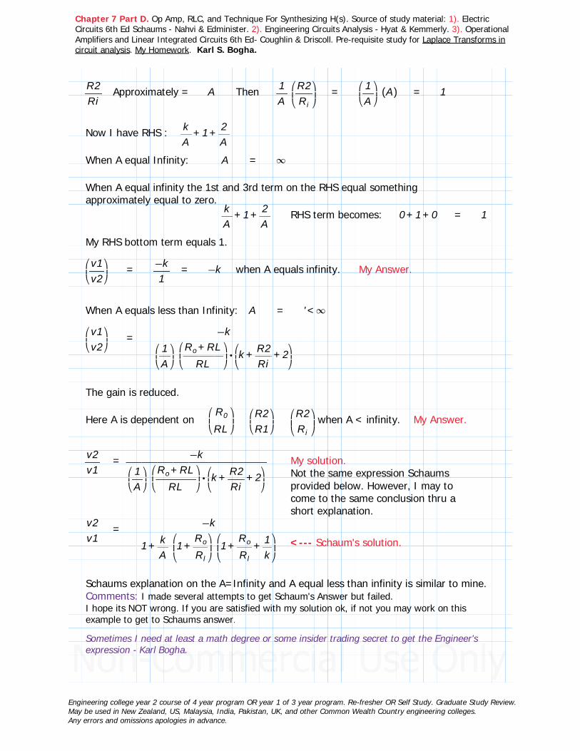
Chapter 7 Part D. Op Amp, RLC, and Technique For Synthesizing H(s). Source of study material: 1). Electric Circuits 6th Ed Schaums - Nahvi & Edminister. 2). Engineering Circuits Analysis - Hyat & Kemmerly. 3). Operational Amplifiers and Linear Integrated Circuits 6th Ed- Coughlin & Driscoll. Pre-requisite study for Laplace Transforms in circuit analysis. My Homework. Karl S. Bogha.
――R2Ri
Approximately = A Then ―1A⎛⎜⎝――R2Ri
⎞⎟⎠
= ⎛⎜⎝―1A⎞⎟⎠
((A)) = 1
Now I have RHS : ++―kA
1 ―2A
When A equal Infinity: A = ∞
When A equal infinity the 1st and 3rd term on the RHS equal something approximately equal to zero.
++―kA
1 ―2A
RHS term becomes: ++0 1 0 = 1
My RHS bottom term equals 1.
⎛⎜⎝―v1v2⎞⎟⎠
= ――−k1
= −k when A equals infinity. My Answer.
When A equals less than Infinity: A = <' ∞
⎛⎜⎝―v1v2⎞⎟⎠
= ――――――――――−k
⋅⎛⎜⎝―1A⎞⎟⎠⎛⎜⎝―――
+Ro RLRL
⎞⎟⎠⎛⎜⎝
++k ――R2Ri
2⎞⎟⎠
The gain is reduced.
Here A is dependent on⎛⎜⎝――R0
RL⎞⎟⎠⎛⎜⎝――R2R1⎞⎟⎠⎛⎜⎝――R2Ri
⎞⎟⎠
when A < infinity. My Answer.
―v2v1
= ――――――――――−k
⋅⎛⎜⎝―1A⎞⎟⎠⎛⎜⎝―――
+Ro RLRL
⎞⎟⎠⎛⎜⎝
++k ――R2Ri
2⎞⎟⎠
My solution.Not the same expression Schaums provided below. However, I may to come to the same conclusion thru a short explanation.
―v2v1
= ―――――――――−k
+1 ―kA⎛⎜⎝
+1 ―Ro
Rl
⎞⎟⎠
⎛⎜⎝
++1 ―Ro
Rl―1k⎞⎟⎠
<--- Schaum's solution.
Schaums explanation on the A=Infinity and A equal less than infinity is similar to mine.Comments: I made several attempts to get Schaum's Answer but failed. I hope its NOT wrong. If you are satisfied with my solution ok, if not you may work on this example to get to Schaums answer.
Sometimes I need at least a math degree or some insider trading secret to get the Engineer's expression - Karl Bogha.
Engineering college year 2 course of 4 year program OR year 1 of 3 year program. Re-fresher OR Self Study. Graduate Study Review.May be used in New Zealand, US, Malaysia, India, Pakistan, UK, and other Common Wealth Country engineering colleges.Any errors and omissions apologies in advance.

Chapter 7 Part D. Op Amp, RLC, and Technique For Synthesizing H(s). Source of study material: 1). Electric Circuits 6th Ed Schaums - Nahvi & Edminister. 2). Engineering Circuits Analysis - Hyat & Kemmerly. 3). Operational Amplifiers and Linear Integrated Circuits 6th Ed- Coughlin & Driscoll. Pre-requisite study for Laplace Transforms in circuit analysis. My Homework. Karl S. Bogha.
Section 5.16 A Simple Op Amp Model.
Last section the examples were based on a closed loop gain A.
The same opamp model 741 can be connected in an open or closed loop gain. The deviation of a real opamp from ideal model is most noticeable in the open loop gain A.
Real opamp has a finite open loop gain which decreases with frequency, and brings in a phase angle change in the signal.
This phase angle change has to be taken into consideration when frequency response is considered.
Example 5.23: (Decibel dB) - Returning to Section 5.14 Decibel dB.
Same circuit for example 5.18 not similar problem.
Find the gain of the filter of example 5.18 as a function of frequency and express it in dB. Specify:a). its dc valueb). its 3 dB attenuation frequencyc). its value at 10 kHzd). its high frequency asymptote
Basically this is called a filter circuit in filters course. Parallel RC circuit.
Just get to know this can be something frequency response related, its a filter chapter/course content. Get to know frequency and filter. I did not provide filter theory.No need to hero it, just an example.
Solution:
From Example 5.18, I got this expression:+⋅10−3
――dv2
dtv2 = −v1
Here v1(t) = V1 cos (2 PI f t).
From the understanding of that theory there is a change in phase angle and magnitude, which results with v2(t) = V1 cos(2 PI f t - Phase Angle Theta).v1 ((t)) = V1cos ((2 πft)) v2 ((t)) = V2cos (( −2 πft θ))
Next a few given expressions, active filter related, ie OpAmp and RCL components. Dont need to fuss about where these come from you can check your active filter chapter in your textbook.
Engineering college year 2 course of 4 year program OR year 1 of 3 year program. Re-fresher OR Self Study. Graduate Study Review.May be used in New Zealand, US, Malaysia, India, Pakistan, UK, and other Common Wealth Country engineering colleges.Any errors and omissions apologies in advance.

Chapter 7 Part D. Op Amp, RLC, and Technique For Synthesizing H(s). Source of study material: 1). Electric Circuits 6th Ed Schaums - Nahvi & Edminister. 2). Engineering Circuits Analysis - Hyat & Kemmerly. 3). Operational Amplifiers and Linear Integrated Circuits 6th Ed- Coughlin & Driscoll. Pre-requisite study for Laplace Transforms in circuit analysis. My Homework. Karl S. Bogha.
Gain: ――V2V1
= ――――1
‾‾‾‾‾‾‾+1 ⎛⎜⎝―ffc
⎞⎟⎠
2θ = −tan−1 ⎛
⎜⎝―ffc
⎞⎟⎠
Gain can us ratio of voltages, powers, and this is one here is something from Filter Theory using frequency.
ωC = ――1
RC= 2 πfC Active filter notes:
Cutoff frequency wc is that frequency of Ei, where |Acl| is reduced to 0.707 times its low frequency value.
≔R ⋅1 103 Ohm ≔C ⋅1 10−6 F
=――1⋅R C
1000 Make f = 0, fc = 159.1549. Then that results in 1/Sqrt (1) = 1. Log 1 to base 10 = 0.f=0 for dc.Answer 0 dB.
ωC = 1000 = 2 πfC
fC = =――1000⋅2 π
159.1549Attenuation would be -ve sign.
Gain_in_dB = 20 log10|||――V2V1
|||
= ⋅−20 log10
‾‾‾‾‾‾‾‾+1 ⎛⎜⎝―f
fC
⎞⎟⎠
2
dB
The expression above can be plottedfor values of f. Resulting in Gain Vs Frequency, plotted in log scale.a). DC signal frequency equal zero. f = 0.
Gain: ――V2V1
= ―――――1‾‾‾‾‾‾‾‾‾
+1 ⎛⎜⎝――0159⎞⎟⎠
2= ――1
‾‾1= 1
=⋅20 log (( ,1 10[[ ]])) 0[[ ]] dc gain = 0 Answer.
b) 3 dB attenuation frequency :
Where: +1 ⎛⎜⎝―f
fC
⎞⎟⎠
2
= 2 <---Is the same as: +1 ⎛⎜⎝――ωωC
⎞⎟⎠
2
= 2
+1 ⎛⎜⎝――2 πf
2 πfC
⎞⎟⎠
2
= 2
ωC = 1000 = 2 πfC This was calculated above.
+1 ⎛⎜⎝――2 πf1000
⎞⎟⎠
2
= 2 For this expression to equal 2 the numerator must equal what? 1000.
ω = 1000 = 1 kHz. Answer.
+1 ⎛⎜⎝――ωωC
⎞⎟⎠
2
= +1 ⎛⎜⎝――10001000
⎞⎟⎠
2
= +1 1 = 2
Engineering college year 2 course of 4 year program OR year 1 of 3 year program. Re-fresher OR Self Study. Graduate Study Review.May be used in New Zealand, US, Malaysia, India, Pakistan, UK, and other Common Wealth Country engineering colleges.Any errors and omissions apologies in advance.

Chapter 7 Part D. Op Amp, RLC, and Technique For Synthesizing H(s). Source of study material: 1). Electric Circuits 6th Ed Schaums - Nahvi & Edminister. 2). Engineering Circuits Analysis - Hyat & Kemmerly. 3). Operational Amplifiers and Linear Integrated Circuits 6th Ed- Coughlin & Driscoll. Pre-requisite study for Laplace Transforms in circuit analysis. My Homework. Karl S. Bogha.
c). Gain at f equal 10 kHz:‾‾‾‾‾‾‾‾
+1 ⎛⎜⎝―f
fC
⎞⎟⎠
2
=‾‾‾‾‾‾‾‾‾‾‾
+1 ⎛⎜⎝―――100001000
⎞⎟⎠
2
= ‾‾‾‾‾‾‾+1 ((10))2 = =‾‾‾101 10.05
Gain: ⋅⋅−20 log10
‾‾‾‾‾‾‾‾+1 ⎛⎜⎝―f
fC
⎞⎟⎠
2
= ⋅⋅−20 log10 10.05
=log (( ,10.05 10[[ ]])) 1.0022[[ ]]
= =⋅−20 log (( ,10.05 10[[ ]])) −20.0433[[ ]]
= −20.04 dB
OR to whole number gain = −20 dB Answer.
d). At high frequencies the gain is:Gain in dB = ⋅20 log10 ((gain))
gain =|||―v2
v1
|||
v2 the output andv1 the input voltage.
⋅20 log10⎛⎜⎝―v2
v1
⎞⎟⎠
= ⋅−20 log10⎛⎜⎝―ff0
⎞⎟⎠
dB
Let high frequency be 100kHz ‾‾‾‾‾‾‾‾‾‾‾+1 ⎛⎜⎝―――100000
1000⎞⎟⎠
2
= ‾‾‾‾‾‾‾‾+1 ((100))2= =‾‾‾‾‾10001 100.005
Gain: ⋅⋅−20 log10
‾‾‾‾‾‾‾‾+1 ⎛⎜⎝―f
fC
⎞⎟⎠
2
= ⋅⋅−20 log10 100.05
= =⋅−20 log (( ,100.05 10[[ ]])) −40.0043[[ ]]
= −40 dB
Increased the frequency to 100kHz, the gain is a drop to -40dB.
This is a -20dB drop when frequency was 10 kHz. The gain decreases by 20dB for each decade of frequency increase, 1khz-10kHz-100kHz-...... Answer.
Comments: A little less grounded. This is not a filter's topic.However, adequate for my purpose in opamp circuit study. Later, maybe some relevant similar calculations. Not a problem here.
Engineering college year 2 course of 4 year program OR year 1 of 3 year program. Re-fresher OR Self Study. Graduate Study Review.May be used in New Zealand, US, Malaysia, India, Pakistan, UK, and other Common Wealth Country engineering colleges.Any errors and omissions apologies in advance.

Chapter 7 Part D. Op Amp, RLC, and Technique For Synthesizing H(s). Source of study material: 1). Electric Circuits 6th Ed Schaums - Nahvi & Edminister. 2). Engineering Circuits Analysis - Hyat & Kemmerly. 3). Operational Amplifiers and Linear Integrated Circuits 6th Ed- Coughlin & Driscoll. Pre-requisite study for Laplace Transforms in circuit analysis. My Homework. Karl S. Bogha.
Example 5.26: (Decibel dB) - Open-loop gain.
At low frequencies the magnitude open-loop gain A of a 741 op amp varies as
――――ao
‾‾‾‾‾‾‾+1 ⎛⎜⎝―ffo
⎞⎟⎠
2||A|| = ――V2V1
=
where typically a0 = 200,000 and fo = 5 Hz.
Find a). its dc gainb). the 3 dB attenuation frequencyc). the frequency where the gain is 0 dBd). its high frequency asymptote
Solution:
a). Gain in dB = ⋅20 log10 ((gain))Gain_a0 = 200000
= 2 x 100000 Set it in the 100,000 decade form.= +20 log102 20 log10100000= +20 log (( ,2 10[[ ]])) ⋅20 log (( ,100000 10[[ ]]))
=20 log (( ,2 10[[ ]])) 6.0206[[ ]]=⋅20 log (( ,100000 10[[ ]])) 100[[ ]] <-- OR 2 x 10^5, is Log
10^5 to base 10 = 5, next times 20 = 100. Thats one simple way from Math.
= +6.0206 100= 106 dB. Answer.
b). +1 ⎛⎜⎝―ff0
⎞⎟⎠
2
= 2 Given fo = 5 Hz. Find f ?
To solve the expression above f can only equal 5.
+1 ⎛⎜⎝―55⎞⎟⎠
2
= +1 12 = +1 1 = 2
f = 5 Hz Answer.
Engineering college year 2 course of 4 year program OR year 1 of 3 year program. Re-fresher OR Self Study. Graduate Study Review.May be used in New Zealand, US, Malaysia, India, Pakistan, UK, and other Common Wealth Country engineering colleges.Any errors and omissions apologies in advance.

Chapter 7 Part D. Op Amp, RLC, and Technique For Synthesizing H(s). Source of study material: 1). Electric Circuits 6th Ed Schaums - Nahvi & Edminister. 2). Engineering Circuits Analysis - Hyat & Kemmerly. 3). Operational Amplifiers and Linear Integrated Circuits 6th Ed- Coughlin & Driscoll. Pre-requisite study for Laplace Transforms in circuit analysis. My Homework. Karl S. Bogha.
c). Gain a0 =‾‾‾‾‾‾‾‾
+1 ⎛⎜⎝―f
fC
⎞⎟⎠
2
200000 =‾‾‾‾‾‾‾
+1 ⎛⎜⎝―f5⎞⎟⎠
2
Solve for frequency f where the gain is 0 dB.
Square both sides:
((200000))2 = +1 ⎛⎜⎝―f5⎞⎟⎠
2
―f2
25= −((200000))2 1 approximately equal = ((200000))2
f2 = ⋅25 ((200000))2 = =⋅25 2000002 ⋅1 1012
f = =‾‾‾‾‾‾⋅1 1012 ⋅1 106
f = 106 Hz Answer.
d). Its frequency asymptote in other words the gain at high frequency?Following the previous example steps. Frequencies at 1kHz, 10kHz, and 100kHz, increments in decades of frequency. For each decade its corresponding gain in dB.Gain at f equal 1 kHz:
‾‾‾‾‾‾‾‾+1 ⎛⎜⎝―f
fC
⎞⎟⎠
2
=‾‾‾‾‾‾‾‾‾‾
+1 ⎛⎜⎝――1000
5⎞⎟⎠
2
= ‾‾‾‾‾‾‾‾+1 ((200))2 = =‾‾‾‾‾40001 200.0025
Gain: ⋅⋅−20 log10
‾‾‾‾‾‾‾‾+1 ⎛⎜⎝―f
fC
⎞⎟⎠
2
= ⋅⋅−20 log10 200
=log (( ,200 10[[ ]])) 2.301[[ ]]= =⋅−20 log (( ,200 10[[ ]])) −46.0206[[ ]]= −46.0 dB
Gain at f equal 10 kHz:‾‾‾‾‾‾‾‾
+1 ⎛⎜⎝―f
fC
⎞⎟⎠
2
=‾‾‾‾‾‾‾‾‾‾‾
+1 ⎛⎜⎝―――10000
5⎞⎟⎠
2
= ‾‾‾‾‾‾‾‾‾+1 ((2000))2 = =‾‾‾‾‾‾‾‾+1 ⋅4 106 2000.0002
Gain: ⋅⋅−20 log10
‾‾‾‾‾‾‾‾+1 ⎛⎜⎝―f
fC
⎞⎟⎠
2
= ⋅⋅−20 log10 2000
=log (( ,2000 10[[ ]])) 3.301[[ ]]= =⋅−20 log (( ,2000 10[[ ]])) −66.0206[[ ]]= −66.0 dB
Engineering college year 2 course of 4 year program OR year 1 of 3 year program. Re-fresher OR Self Study. Graduate Study Review.May be used in New Zealand, US, Malaysia, India, Pakistan, UK, and other Common Wealth Country engineering colleges.Any errors and omissions apologies in advance.

Chapter 7 Part D. Op Amp, RLC, and Technique For Synthesizing H(s). Source of study material: 1). Electric Circuits 6th Ed Schaums - Nahvi & Edminister. 2). Engineering Circuits Analysis - Hyat & Kemmerly. 3). Operational Amplifiers and Linear Integrated Circuits 6th Ed- Coughlin & Driscoll. Pre-requisite study for Laplace Transforms in circuit analysis. My Homework. Karl S. Bogha.
Gain at f equal 100 kHz:‾‾‾‾‾‾‾‾
+1 ⎛⎜⎝―f
fC
⎞⎟⎠
2
=‾‾‾‾‾‾‾‾‾‾‾
+1 ⎛⎜⎝―――100000
5⎞⎟⎠
2
= ‾‾‾‾‾‾‾‾‾‾+1 ((20000))2 = =‾‾‾‾‾‾‾‾+1 ⋅4 108 20000
Gain: ⋅⋅−20 log10
‾‾‾‾‾‾‾‾+1 ⎛⎜⎝―f
fC
⎞⎟⎠
2
= ⋅⋅−20 log10 20000
=log (( ,20000 10[[ ]])) 4.301[[ ]]= =⋅−20 log (( ,20000 10[[ ]])) −86.0206[[ ]]= −86.0 dB
The gain decreases by -20 dB for each decade increase of frequency. Answer.In this case similar to the previous closed loop gain opamp.Comment: 20 dB decrease for every deci (10) frequency increase. This is open loop gain. I had a 20 dB decrease in the closed loop gain for each deci(10) also.
Continuing with the theory side of this section after example 5.26 next page.
Off Topic: Lets Talk Studying at College/University..... Cost Time Value Skills Jobs....Knowledge.
This isnt a filter chapter. Purpose here maybe picking up the circuit analysis for circuits with opamp and RC parts, so that analysis can be built up. Another thing is in a 2 semester course, most these get left out until I get into a specific upper level course. There it starts with some basics, and then picks up with the whole theory on the subject like power systems, machinery, filters,.....
Problem is at that stage, in my time, I had some of these circuit's solving techniques in the circuits course, and the upper level course was not going to go in depth anywhere near a circuits course.
So I am saying obviously a 3rd circuits course is required which has content relevant for the areas that department is teaching. This the engineering colleges may frown on a 3rd circuits course but I am suggesting 4! For them we go there to spend time with them! Goes back at least a over century. Nothing personal.
I were to own and operate an electrical engineering degree granting institution I will have 4 circuits courses. Starting in year 1 semester 1. Ending in year 2 of semester 2 with the 4th course. Then a student can say he's been solving electric circuits at a degree level. Year 3 and 4 has plenty of hours for upper level courses. Hopefully no struggling. Most engineers, 95%, apply one upper level course area for their work. And circuits is content is most of the courses. There is so much more to say with regards to content, example with the 'total understanding of Bode plots', which is skimmed thru until its a controls or filter course or lab. Even then there is a lack of time. Waste of my $. I have a record of failures some say thats a path to success. I say SAVE IT. Its a place we go to get skills not help build one intellectual mind arena. That arena is the university or college. That's if I was operating the college today.
Engineering college year 2 course of 4 year program OR year 1 of 3 year program. Re-fresher OR Self Study. Graduate Study Review.May be used in New Zealand, US, Malaysia, India, Pakistan, UK, and other Common Wealth Country engineering colleges.Any errors and omissions apologies in advance.

Chapter 7 Part D. Op Amp, RLC, and Technique For Synthesizing H(s). Source of study material: 1). Electric Circuits 6th Ed Schaums - Nahvi & Edminister. 2). Engineering Circuits Analysis - Hyat & Kemmerly. 3). Operational Amplifiers and Linear Integrated Circuits 6th Ed- Coughlin & Driscoll. Pre-requisite study for Laplace Transforms in circuit analysis. My Homework. Karl S. Bogha.
Two terminologies to assist in the opamp frequency related circuit problems at an introductory level. Just so I can do some circuit analysis with opamp. For RLC we had the frequency response, similalry the opamp has a frequency response too. That is the only reason. The opamp being an active device, while the R L and C the passive devices.
3-dB Bandwith:
For a low pass filter the 3 dB bandwidth is the frequency at which the opamp circuit's gain falls 3 db below the dc gain.
The open loop bandwidth of the 741 opamp is 5 Hz. <--- That is saying the 3 dB bandwidth is 5 Hz. 3 dB bandwidth is generally reffered to as bandwidth.
Gain-Bandwidth Product (GBP):
The product of the dc gain with the 3 dB bandwidth of the opamp is called its gain bandwidth product. Typical value for 741 opamp is 10^6.
There are a few more points here but it requires explanation from first chapters of filters whether active or passive filters.
Hyat and Kemmerly textbook 'Chapter 14 Frequency Response' has full coverage of Bode diagrams and explains decibels (dB).
But its involved and requires starting from the beginning of the chapter. So that's why I refrained from using it instead briefly used Schaums.
No Deep Thinking Here:There is example 5.27 which I will not be attempting because of the reasons I provided above. Its similar to theorectical proof. Schaums is not a full textbook and for this I need to resort to Hyat and Kemmerly.
Electric circuits is such a subject that all sorts of circuits are in each upper level electrical engineering course. Obviously they can't all be covered within a given 2 semester schedule.
Engineering college year 2 course of 4 year program OR year 1 of 3 year program. Re-fresher OR Self Study. Graduate Study Review.May be used in New Zealand, US, Malaysia, India, Pakistan, UK, and other Common Wealth Country engineering colleges.Any errors and omissions apologies in advance.

Chapter 7 Part D. Op Amp, RLC, and Technique For Synthesizing H(s). Source of study material: 1). Electric Circuits 6th Ed Schaums - Nahvi & Edminister. 2). Engineering Circuits Analysis - Hyat & Kemmerly. 3). Operational Amplifiers and Linear Integrated Circuits 6th Ed- Coughlin & Driscoll. Pre-requisite study for Laplace Transforms in circuit analysis. My Homework. Karl S. Bogha.
Section 5.17 Comparator.
Comparator circuit is a critical circuit. A chapter is dedicated to it in C&D. By the name itself, comparator, with the programming course work I had, comparing two values was very necessary, and required before the next step could progress.
Thats what we have here. Comparator.
Circuit above compares voltage v1 with reference voltage level vo.The circuit is an open loop gain opamp.This gain is very high (open loop).The opamp circuit output is v2.
The output v2 = +Vcc when v1 > vo, or v2 = -Vcc when v1 < vo.
The technical way of expressing: v2 = +' Vcc
sgn −v1 v0[[ ]]sgn stands for 'sign of'
For v0 = 0sgn −v1 0[[ ]]sgn v1[[ ]]
+' Vcc >v1 0v2 = Vcc sgn [v1] =
−' Vcc <v1 0
Next an example.
Engineering college year 2 course of 4 year program OR year 1 of 3 year program. Re-fresher OR Self Study. Graduate Study Review.May be used in New Zealand, US, Malaysia, India, Pakistan, UK, and other Common Wealth Country engineering colleges.Any errors and omissions apologies in advance.

Chapter 7 Part D. Op Amp, RLC, and Technique For Synthesizing H(s). Source of study material: 1). Electric Circuits 6th Ed Schaums - Nahvi & Edminister. 2). Engineering Circuits Analysis - Hyat & Kemmerly. 3). Operational Amplifiers and Linear Integrated Circuits 6th Ed- Coughlin & Driscoll. Pre-requisite study for Laplace Transforms in circuit analysis. My Homework. Karl S. Bogha.
Example 5.28
In the circuit to the leftlet Vcc = 5V, vo = 0V, and v1 = sin wt.Find v2?
Solution:
I want to solve for the condition provided below.
+' Vcc >v1 0v2 = Vcc sgn [v1] =
−' Vcc <v1 0
I have a sinusoidal input signal. Need to identify the period-frequency so I can distinguish when its positive and when its negative at the input.
v1 = >sin ((ωt)) 0
ω = 2 πf f = ――ω
2 π
T = ―1f
= ――2 πω
This is one period.
Since its sinusoidal the signal will change sign half way thru each period.Break the period T to reflect the sign change.
First half of period <<0 t ―πω
2 PI/w divided by 2 = PI/w.
Second half of period <<―πω
t ――2 πω
Engineering college year 2 course of 4 year program OR year 1 of 3 year program. Re-fresher OR Self Study. Graduate Study Review.May be used in New Zealand, US, Malaysia, India, Pakistan, UK, and other Common Wealth Country engineering colleges.Any errors and omissions apologies in advance.

Chapter 7 Part D. Op Amp, RLC, and Technique For Synthesizing H(s). Source of study material: 1). Electric Circuits 6th Ed Schaums - Nahvi & Edminister. 2). Engineering Circuits Analysis - Hyat & Kemmerly. 3). Operational Amplifiers and Linear Integrated Circuits 6th Ed- Coughlin & Driscoll. Pre-requisite study for Laplace Transforms in circuit analysis. My Homework. Karl S. Bogha.
Because of the simplicity of the circuit, the output v2 is oscillating between +Vcc and -Vcc.
+' Vcc >v1 0 <<0 t ―πωv2 = Vcc sgn [v1] =
−' Vcc <v1 0 <<―πω
t ――2 πω
First half of period:<<0 t ―πω
v1 = >sin ((ωt)) 0 v2 = 5 V
Second half of period:<<―
πω
t ――2 πω
v1 = <sin ((ωt)) 0 v2 = −5 V
Presenting the answer like the theory part:+' 5 V >v1 0 <<0 t ―
πωv2 = Vcc sgn [v1] =
−' 5 V <v1 0 <<―πω
t ――2 πω
The output waveform is NOT sinusoidal. It remains constant for the time interval.Thus its a square pulse, +5V and -5V. Agreed? Yes, constant for the time interval.The output waveform is quite an achivement for the opamp. It oscillates between +5 and -5V.
Engineering college year 2 course of 4 year program OR year 1 of 3 year program. Re-fresher OR Self Study. Graduate Study Review.May be used in New Zealand, US, Malaysia, India, Pakistan, UK, and other Common Wealth Country engineering colleges.Any errors and omissions apologies in advance.

Chapter 7 Part D. Op Amp, RLC, and Technique For Synthesizing H(s). Source of study material: 1). Electric Circuits 6th Ed Schaums - Nahvi & Edminister. 2). Engineering Circuits Analysis - Hyat & Kemmerly. 3). Operational Amplifiers and Linear Integrated Circuits 6th Ed- Coughlin & Driscoll. Pre-requisite study for Laplace Transforms in circuit analysis. My Homework. Karl S. Bogha.
Window Comparator:
This opamp circuit consists of 2 opams connections. Schaum gives a very light description. C&D has a circuit.I dont want to dwell on this here, check in your circuits or electronic textbook.Basically this circuit can check when the voltage falls between a range. 2 comparators set at two limits, V_TL and V_TH, voltage threshold/limit level low and high. So if a certain input voltage v1 from a supply source is within the upper and lower limit, the circuit's logic may result with an ON, otherwise OFF.
Such a circuit is called a 'window comparator'.
Its output v2 is given by:
+' Vcc <<VTL v1 VTHv2 = Vcc sgn [v1] =
−' Vcc otherwise
Section 5.18 Flash Analog To Digital Converter.
Using the window comparator circuit, and having n comparators in parallel, an analog to digital signal converter can be created. For this study in the circuits textbook. Schaums has a basic example following the notes. I will not do this here, because similarly there are many other main topics and sub topics. Have to drop the pen sometime.
Next.
I want to solve a few relevant examples for my study and skills.These examples try to fit the chapter 13 Hyat and Kemmerly notes where opamp circuits were given. Thats the aim.
After the few Schaums examples, I work the Hyat Kemmerly theory section opamp circuits.
Then returning to where I left off in Hyat Kemmerly.
Next Section 3 are related solved example problems in opamp circuits.
Engineering college year 2 course of 4 year program OR year 1 of 3 year program. Re-fresher OR Self Study. Graduate Study Review.May be used in New Zealand, US, Malaysia, India, Pakistan, UK, and other Common Wealth Country engineering colleges.Any errors and omissions apologies in advance.

Chapter 7 Part 3D. Op Amp, RLC, and Technique For Synthesizing H(s). Source of study material: 1). Electric Circuits 6th Ed Schaums - Nahvi & Edminister. 2). Engineering Circuits Analysis - Hyat & Kemmerly. 3). Operational Amplifiers and Linear Integrated Circuits 6th Ed- Coughlin & Driscoll. Pre-requisite study for Laplace Transforms in circuit analysis. My Homework. Karl S. Bogha.
Part 3 D: Section 3.
RLC Higher Order Circuits - Continuing Notes With Solved Examples.
Section 3: Fully solving partially solved examples, partially solved problems, and supplementary problems.
Problems are related to Op Amp circuits.
Primarily the topics covered in Schaums.
Purpose is toget an understanding on how to approach solving Op Amp Active circuits. These are circuits with Op Amp and R L and C components.
There is a special topic covered from Chapter 7 of 4th edition of Hyat and Kemmerly the topic is on The Lossless LC Circuit from section 7-8. This topic is relevant to RLC studies.
Continuing with the final Section 4.
Picking up from where I left in end of Part 3B Section 13-8 A Technique For Synthesizing The Voltage Ratio H(s) = Vout / Vin.
Apologies for any errors and omissions.
Engineering college year 2 course of 4 year program OR year 1 of 3 year program. Re-fresher OR Self Study. Graduate Study Review.May be used in New Zealand, US, Malaysia, India, Pakistan, UK, and other Common Wealth Country engineering colleges.Any errors and omissions apologies in advance.

Chapter 7 Part D. Op Amp, RLC, and Technique For Synthesizing H(s). Source of study material: 1). Electric Circuits 6th Ed Schaums - Nahvi & Edminister. 2). Engineering Circuits Analysis - Hyat & Kemmerly. 3). Operational Amplifiers and Linear Integrated Circuits 6th Ed- Coughlin & Driscoll. Pre-requisite study for Laplace Transforms in circuit analysis. My Homework. Karl S. Bogha.
Section 3.
Schaums Example Problem Chapter 5 of 6th Edition,And A Few Opamp Theory and Examples From 'Engineering Circuit Analysis'Hyat & Kemmerly.
Problem 5.1:
In the circuit below, letvs = 20V, Rs = 10 ohm, Ri = 990 ohm, k = 5, and Ro = 3 ohm.Find a). Thevenin equivalent circuit seen by RL b). v2 and the power dissipated in RL for RL = 0.5, 1, 3, 5, 10, 100, and 1000.
Solution:k = 5
v2 = kv1 = 5 v1 This voltage is called open circuit voltage.
Voltage across AB equal 5v1.
Current entering point A is ――kv1Ro
= ――5 v1
3= is This current is called
the short circuit current.
With the circuit information provided, I can find v1 on the left side of the circuit.
ileft = ―――vs
+Rs Ri
v1 is the voltage just past the resistor Rs, thus v1 = i_left Ri.
v1 = ileftRi =⎛⎜⎝―――
vs
+Rs Ri
⎞⎟⎠
Ri = ⋅⎛⎜⎝―――
Ri
+Rs Ri
⎞⎟⎠
vs
Engineering college year 2 course of 4 year program OR year 1 of 3 year program. Re-fresher OR Self Study. Graduate Study Review.May be used in New Zealand, US, Malaysia, India, Pakistan, UK, and other Common Wealth Country engineering colleges.Any errors and omissions apologies in advance.

Chapter 7 Part D. Op Amp, RLC, and Technique For Synthesizing H(s). Source of study material: 1). Electric Circuits 6th Ed Schaums - Nahvi & Edminister. 2). Engineering Circuits Analysis - Hyat & Kemmerly. 3). Operational Amplifiers and Linear Integrated Circuits 6th Ed- Coughlin & Driscoll. Pre-requisite study for Laplace Transforms in circuit analysis. My Homework. Karl S. Bogha.
v1 = ⋅⎛⎜⎝―――
Ri
+Rs Ri
⎞⎟⎠
vs = =⋅⎛⎜⎝―――
990+10 990
⎞⎟⎠
20 19.8 V
Solve for v2: v2 = 5 v1 = =⋅5 19.8 99 V
v2 is the open circuit voltage seen across AB: voc = v2 = 99 V
i_short circuit current: is = =―――⋅5 19.8
333 A
The reduced Thevenin circuit is to the left. Thevenin voltage is 99V. vTh = voc = 99 V Answer.
What is the Thevenin resitance seen across AB?
Rth = ――voc
isc
Rth = =―9933
3 Ohm Answer.
Next, include the resistor load RL into the circuit analysis.This would mean I am seeking the voltage v2.
v2 = ⋅⎛⎜⎝―――
RL
+RL RTh
⎞⎟⎠
vTh Correct, voltage division with the use of Thevenin voltage, and Thevenin resistance.
v2 = ―――99 RL
+RL 3This expression 'tailor made' for RL!Or expression suits for values of RL.
Next an expression of power for various values of RL.
p = ⋅v i = ⋅v ⎛⎜⎝―vR⎞⎟⎠
= ―v2
R
pL = ――v22
RL= ―――
⎛⎜⎝―――99 RL
+RL 3⎞⎟⎠
RL= ⋅⎛⎜⎝―――99 RL
+RL 3⎞⎟⎠⎛⎜⎝――
1RL
⎞⎟⎠
= ⎛⎜⎝―――
99+RL 3⎞⎟⎠
Engineering college year 2 course of 4 year program OR year 1 of 3 year program. Re-fresher OR Self Study. Graduate Study Review.May be used in New Zealand, US, Malaysia, India, Pakistan, UK, and other Common Wealth Country engineering colleges.Any errors and omissions apologies in advance.
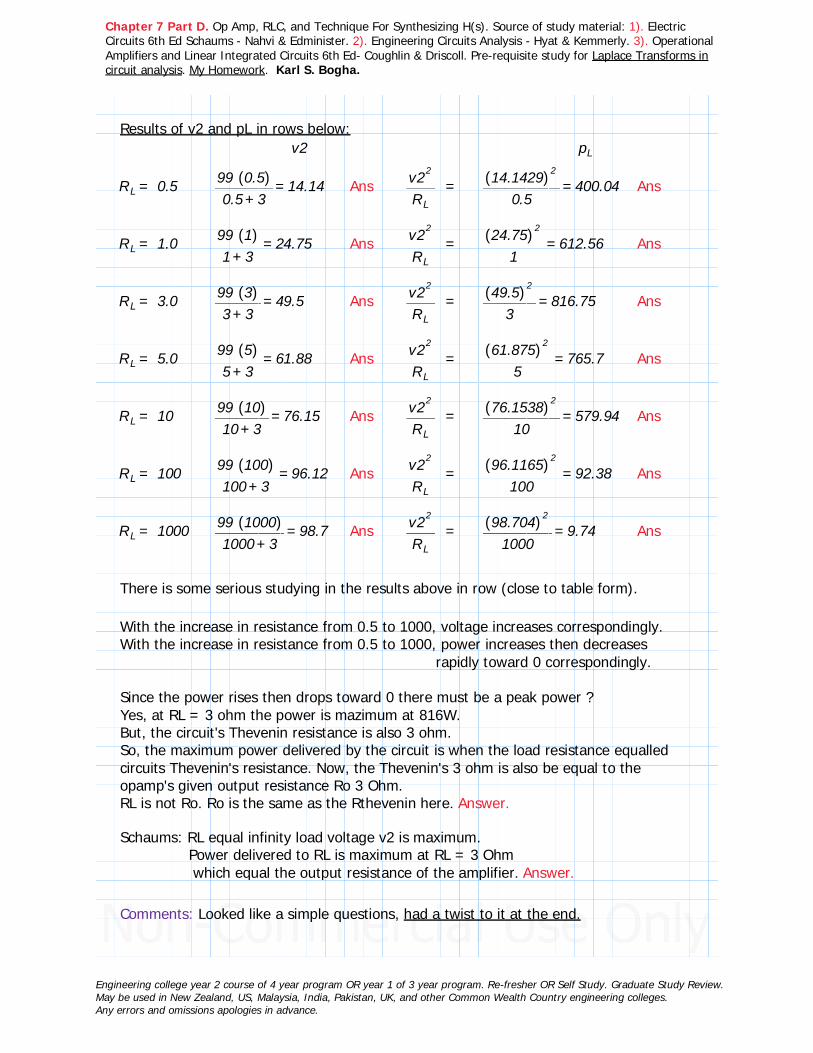
Chapter 7 Part D. Op Amp, RLC, and Technique For Synthesizing H(s). Source of study material: 1). Electric Circuits 6th Ed Schaums - Nahvi & Edminister. 2). Engineering Circuits Analysis - Hyat & Kemmerly. 3). Operational Amplifiers and Linear Integrated Circuits 6th Ed- Coughlin & Driscoll. Pre-requisite study for Laplace Transforms in circuit analysis. My Homework. Karl S. Bogha.
Results of v2 and pL in rows below:v2 pL
RL = 0.5 =―――99 ((0.5))
+0.5 314.14 Ans ――
v22
RL= =――――
((14.1429))2
0.5400.04 Ans
RL = 1.0 =―――99 ((1))
+1 324.75 Ans ――
v22
RL= =―――
((24.75))2
1612.56 Ans
RL = 3.0 =―――99 ((3))
+3 349.5 Ans ――
v22
RL= =―――
((49.5))2
3816.75 Ans
RL = 5.0 =―――99 ((5))
+5 361.88 Ans ――
v22
RL= =――――
((61.875))2
5765.7 Ans
RL = 10 =―――99 ((10))
+10 376.15 Ans ――
v22
RL= =――――
((76.1538))2
10579.94 Ans
RL = 100 =―――99 ((100))
+100 396.12 Ans ――
v22
RL= =――――
((96.1165))2
10092.38 Ans
RL = 1000 =――――99 ((1000))
+1000 398.7 Ans ――
v22
RL= =――――
((98.704))2
10009.74 Ans
There is some serious studying in the results above in row (close to table form).
With the increase in resistance from 0.5 to 1000, voltage increases correspondingly.With the increase in resistance from 0.5 to 1000, power increases then decreases rapidly toward 0 correspondingly.
Since the power rises then drops toward 0 there must be a peak power ?Yes, at RL = 3 ohm the power is mazimum at 816W.But, the circuit's Thevenin resistance is also 3 ohm.So, the maximum power delivered by the circuit is when the load resistance equalled circuits Thevenin's resistance. Now, the Thevenin's 3 ohm is also be equal to the opamp's given output resistance Ro 3 Ohm. RL is not Ro. Ro is the same as the Rthevenin here. Answer.
Schaums: RL equal infinity load voltage v2 is maximum. Power delivered to RL is maximum at RL = 3 Ohm which equal the output resistance of the amplifier. Answer.
Comments: Looked like a simple questions, had a twist to it at the end.
Engineering college year 2 course of 4 year program OR year 1 of 3 year program. Re-fresher OR Self Study. Graduate Study Review.May be used in New Zealand, US, Malaysia, India, Pakistan, UK, and other Common Wealth Country engineering colleges.Any errors and omissions apologies in advance.

Chapter 7 Part D. Op Amp, RLC, and Technique For Synthesizing H(s). Source of study material: 1). Electric Circuits 6th Ed Schaums - Nahvi & Edminister. 2). Engineering Circuits Analysis - Hyat & Kemmerly. 3). Operational Amplifiers and Linear Integrated Circuits 6th Ed- Coughlin & Driscoll. Pre-requisite study for Laplace Transforms in circuit analysis. My Homework. Karl S. Bogha.
Problem 5.2 (Gain G) :
In the circuits A and B, let R1 = 1 kohm and R2=5 kohm.Find the gains G+ = v2/vs circuit A (notes example 3), and
G - = v2/vs circuit B (notes example 4), for k = 1, 2, 4, 6, 8, 10, 100, 1000, and infinity ?Compare the results?
Circuit A is figure Theory/Notes Example 3.Feedback loop.
Circuit B is figure Theory/Notes Example 4.Open loop.The Gain kv polarity is reversed to -ve.
Solution:Circuit A: ―
v2vs
= ―――――⋅R2 k−+R2 R1 ⋅R1 k
See Notes-Example 3 for this expression --->
= ―――――――⋅5000 k−+5000 1000 ⋅1000 k
Simplify keep at k or divide by 1000.
G +' ' = ――⋅5 k−6 k
Circuit B: Solution given by Schaum―v2vs
= ―――――⋅−R2 k
++R2 R1 ⋅R1 kCircuit differ from A by polarity, add -ve sign.
= ―――――――⋅−5000 k
++5000 1000 ⋅1000 k
G −' ' = −――⋅5 k+6 k
Engineering college year 2 course of 4 year program OR year 1 of 3 year program. Re-fresher OR Self Study. Graduate Study Review.May be used in New Zealand, US, Malaysia, India, Pakistan, UK, and other Common Wealth Country engineering colleges.Any errors and omissions apologies in advance.

Chapter 7 Part D. Op Amp, RLC, and Technique For Synthesizing H(s). Source of study material: 1). Electric Circuits 6th Ed Schaums - Nahvi & Edminister. 2). Engineering Circuits Analysis - Hyat & Kemmerly. 3). Operational Amplifiers and Linear Integrated Circuits 6th Ed- Coughlin & Driscoll. Pre-requisite study for Laplace Transforms in circuit analysis. My Homework. Karl S. Bogha.
Next a table of values for G+ and G- for each k.
k G +' ' Closed Loop G −' ' Open Loop
1 =――⋅5 1−6 1
1 =−――⋅5 1+6 1
−0.71
2 =――⋅5 2−6 2
2.5 =−――⋅5 2+6 2
−1.25
4 =――⋅5 4−6 4
10 =−――⋅5 4+6 4
−2
6 ――⋅5 6−6 6
= ∞ <--- =−――⋅5 6+6 6
−2.5
8 =――⋅5 8−6 8
−20 =−――⋅5 8+6 8
−2.86
10 =――⋅5 10−6 10
−12.5 =−――⋅5 10+6 10
−3.13
100 =―――⋅5 100−6 100
−5.32 =−―――⋅5 100+6 100
−4.72
1000 =―――⋅5 1000−6 1000
−5.03 =−―――⋅5 1000+6 1000
−4.97
∞ ――⋅5 ∞−6 ∞
= ――⋅5 ∞−' ∞
= −5<--- −――⋅5 ∞+6 ∞
= ―――⋅−5 ∞+' ∞
= −5<---
As k increases, the resistance being multiplied by k, the gain G+ increases to INFINITY when k=6, then drops back down low to a final value of -5. Whilst the gain G- starts at -0.71 and gradually end at -5.G- gain is stable compared to G+, which gain G+ goes into infinity at k=6 is instablity.
Gain G- monotonically approaches the limit -5.Monotonically meaning the change is NOT increasing and decreasing,rather increasing or decreasing ONLY.
G- is negative and increases slowly to -5.G+ starts positive then to infinity then goes negative and settles to -5.Comment: Interesting observations. Gained skills.
Engineering college year 2 course of 4 year program OR year 1 of 3 year program. Re-fresher OR Self Study. Graduate Study Review.May be used in New Zealand, US, Malaysia, India, Pakistan, UK, and other Common Wealth Country engineering colleges.Any errors and omissions apologies in advance.
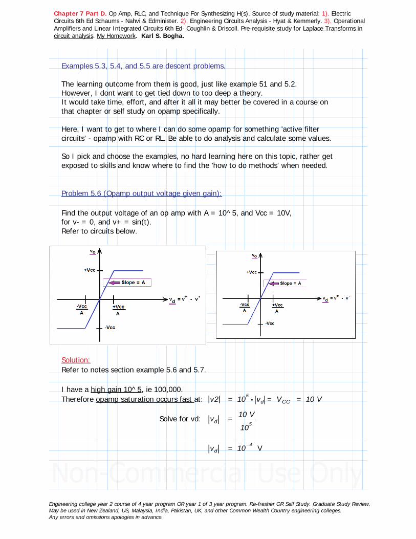
Chapter 7 Part D. Op Amp, RLC, and Technique For Synthesizing H(s). Source of study material: 1). Electric Circuits 6th Ed Schaums - Nahvi & Edminister. 2). Engineering Circuits Analysis - Hyat & Kemmerly. 3). Operational Amplifiers and Linear Integrated Circuits 6th Ed- Coughlin & Driscoll. Pre-requisite study for Laplace Transforms in circuit analysis. My Homework. Karl S. Bogha.
Examples 5.3, 5.4, and 5.5 are descent problems.
The learning outcome from them is good, just like example 51 and 5.2.However, I dont want to get tied down to too deep a theory.It would take time, effort, and after it all it may better be covered in a course on that chapter or self study on opamp specifically.
Here, I want to get to where I can do some opamp for something 'active filter circuits' - opamp with RC or RL. Be able to do analysis and calculate some values.
So I pick and choose the examples, no hard learning here on this topic, rather get exposed to skills and know where to find the 'how to do methods' when needed.
Problem 5.6 (Opamp output voltage given gain):
Find the output voltage of an op amp with A = 10^5, and Vcc = 10V,for v- = 0, and v+ = sin(t).Refer to circuits below.
Solution:Refer to notes section example 5.6 and 5.7.
I have a high gain 10^5, ie 100,000. Therefore opamp saturation occurs fast at: ||v2|| = ⋅105 ||vd|| = VCC = 10 V
Solve for vd: ||vd|| = ――10 V
105
||vd|| = 10−4 V
Engineering college year 2 course of 4 year program OR year 1 of 3 year program. Re-fresher OR Self Study. Graduate Study Review.May be used in New Zealand, US, Malaysia, India, Pakistan, UK, and other Common Wealth Country engineering colleges.Any errors and omissions apologies in advance.

Chapter 7 Part D. Op Amp, RLC, and Technique For Synthesizing H(s). Source of study material: 1). Electric Circuits 6th Ed Schaums - Nahvi & Edminister. 2). Engineering Circuits Analysis - Hyat & Kemmerly. 3). Operational Amplifiers and Linear Integrated Circuits 6th Ed- Coughlin & Driscoll. Pre-requisite study for Laplace Transforms in circuit analysis. My Homework. Karl S. Bogha.
Absolute value of vd = 10^-4.vd = 0.0001andvd = -0.0001
I am looking at the opamp with no external components connected.I can ignore the linear interval because vd is small. That interval shown below. Then what becomes of the plot, see following plot.
<--- Showing the interval region ignored.
<--- Now without the slope.vd >0andvd<0.
Resulting with a range for v2:
+' 10 V >vd 0v2 =
−' 10 V <vd 0
Engineering college year 2 course of 4 year program OR year 1 of 3 year program. Re-fresher OR Self Study. Graduate Study Review.May be used in New Zealand, US, Malaysia, India, Pakistan, UK, and other Common Wealth Country engineering colleges.Any errors and omissions apologies in advance.

Chapter 7 Part D. Op Amp, RLC, and Technique For Synthesizing H(s). Source of study material: 1). Electric Circuits 6th Ed Schaums - Nahvi & Edminister. 2). Engineering Circuits Analysis - Hyat & Kemmerly. 3). Operational Amplifiers and Linear Integrated Circuits 6th Ed- Coughlin & Driscoll. Pre-requisite study for Laplace Transforms in circuit analysis. My Homework. Karl S. Bogha.
Given in the problem statement v+ = sin(t), and v- = 0.
vd = (v+) - (v-) = sin(t) - 0 = sin(t).
There is vd in relation to A, and vd in relation to the signal connected across the +ve and -ve terminals of the opamp.
vd ((t)) = sin ((t))
That is clearly the sin of t, which is saying 0 to 2 PI is one cycle.Half positive cycle and half negative cycle.
0 to π = positive cycle.
π to 2 π = negative cycle.
+' 10 V <<0 t πv2 =
−' 10 V <<π t 2 π
Now, I have something a little more accurate, the sin(t) termhas is 0 at sin(0) = 0. My earlier situation was ignore the slope because |vd| = 0.0001 which is small. Lets look into making 3 interval of time.1). vd < 02). 0- < vd <0+ ....this is the added interval.3). vd > 0
Instead of 0 in the above expressions, I can make that 10^-4 ie 0.0001
1). vd < -0.00012). -0.0001 < vd <0.0001 3). vd > 0.0001
= −' 10 V <vd 0.0001 V
v2 = ? <<−0.0001 vd 0.0001 V <--- What goes in the '?' spot.
= +' 10 V >vd 0.0001 V
In the A=10^5 analysis. v2 equaled Avd. ||v2|| = ⋅105 ||vd|| = 10 V = VCC
Plug in that expression for v2!
Engineering college year 2 course of 4 year program OR year 1 of 3 year program. Re-fresher OR Self Study. Graduate Study Review.May be used in New Zealand, US, Malaysia, India, Pakistan, UK, and other Common Wealth Country engineering colleges.Any errors and omissions apologies in advance.

Chapter 7 Part D. Op Amp, RLC, and Technique For Synthesizing H(s). Source of study material: 1). Electric Circuits 6th Ed Schaums - Nahvi & Edminister. 2). Engineering Circuits Analysis - Hyat & Kemmerly. 3). Operational Amplifiers and Linear Integrated Circuits 6th Ed- Coughlin & Driscoll. Pre-requisite study for Laplace Transforms in circuit analysis. My Homework. Karl S. Bogha.
What I have now is a more exact v2 using the transfer characteristics of the opamp.
= −' 10 V <vd 0.0001 V
v2 = ⋅105 ||vd|| ><−0.0001 vd 0.0001 V
= +' 10 V >vd 0.0001 V Answer.
Next, the genius of the math and sciences of the engineers, they took it one step yet further. Leaves me grappling to sort their solution.
I have |vd| = sin(t), and |vd| = 10^-4 = 0.0001Since 0.0001 is small the engineers decided to replace sin(t) by t.Sin(0) = 0. So if t is small its near zero, might as well make it equal 0.0001 ie t.Then they provided a new expression reflecting t.
||v2|| = ⋅105 ||vd|| = ⋅105 sin ((t)) = 105 t Correct.
What range would this be on the x-axis? -vd to vd; -vd < t < vd.See the flow of the range in the sketches below.
The slope is positive at t=0, and the signal is centered at t=0. Where A=10^5.v2 = 10^5 (vd) = 10^5 (sin (t - 0) ) at t = 0, 10^5 sin(t) = 10^5 t. The v2 cannot deviate since a range is given.Next range following sketch. Continuing from +vd in sketch above.
Engineering college year 2 course of 4 year program OR year 1 of 3 year program. Re-fresher OR Self Study. Graduate Study Review.May be used in New Zealand, US, Malaysia, India, Pakistan, UK, and other Common Wealth Country engineering colleges.Any errors and omissions apologies in advance.

Chapter 7 Part D. Op Amp, RLC, and Technique For Synthesizing H(s). Source of study material: 1). Electric Circuits 6th Ed Schaums - Nahvi & Edminister. 2). Engineering Circuits Analysis - Hyat & Kemmerly. 3). Operational Amplifiers and Linear Integrated Circuits 6th Ed- Coughlin & Driscoll. Pre-requisite study for Laplace Transforms in circuit analysis. My Homework. Karl S. Bogha.
Figure above signal range shown with v2 = 10V.Followed by the negative slope at Pi.
The slope is negative at t=Pi, and the signal is centered at t=Pi. Where A=-10^5.v2 = -10^5 (vd) = -10^5 (sin( t - Pi ). = -10^5 (t - Pi).
Next continuing with the remainder of the cycle.
Engineering college year 2 course of 4 year program OR year 1 of 3 year program. Re-fresher OR Self Study. Graduate Study Review.May be used in New Zealand, US, Malaysia, India, Pakistan, UK, and other Common Wealth Country engineering colleges.Any errors and omissions apologies in advance.

Chapter 7 Part D. Op Amp, RLC, and Technique For Synthesizing H(s). Source of study material: 1). Electric Circuits 6th Ed Schaums - Nahvi & Edminister. 2). Engineering Circuits Analysis - Hyat & Kemmerly. 3). Operational Amplifiers and Linear Integrated Circuits 6th Ed- Coughlin & Driscoll. Pre-requisite study for Laplace Transforms in circuit analysis. My Homework. Karl S. Bogha.
Signal range shown and the value of v2 = -10V.That wasn't easy for me. You find errors there, youre welcome to correct it.So, the results provided here. These match the previous for the transfer characteristics of the opamp.
v2 = ⋅105 t <<−10−4 t 10−4 seconds
v2 = 10 <<10−4 t −π 10−4 seconds
v2 = ⋅−105 (( −t π)) <<−π 10−4 t +π 10−4 seconds
v2 = −10 <<+π 10−4 t −2 π 10−4 seconds Answer.
Answers above as provided in Schaums.
vd = 0.0001 || +−vd_to_ v_d|| = =+0.0001 0.0001 0.0002
Times 2 over the period since there are 2 slopes: =⋅0.0002 2 0.0004
=―――0.0004⋅2 π
⋅6.3662 10−5 = ⋅64 10−6 This represents the slope error contribution in one cycle, which was ignored, in the first part of the solution (insignificance).
v2 = +' 10 V <<0 t π This range shown to the left does not have the slope. v2 = −' 10 V <<π t 2 π
To appreciate the insignificance of error in ignoring the linear range (slope), during the one period of 2Pi seconds the interval of linear operation is only 4x10^-4s, which gives a ratio of 64x10^-6. - Schaums Answer.
Engineering college year 2 course of 4 year program OR year 1 of 3 year program. Re-fresher OR Self Study. Graduate Study Review.May be used in New Zealand, US, Malaysia, India, Pakistan, UK, and other Common Wealth Country engineering colleges.Any errors and omissions apologies in advance.

Chapter 7 Part D. Op Amp, RLC, and Technique For Synthesizing H(s). Source of study material: 1). Electric Circuits 6th Ed Schaums - Nahvi & Edminister. 2). Engineering Circuits Analysis - Hyat & Kemmerly. 3). Operational Amplifiers and Linear Integrated Circuits 6th Ed- Coughlin & Driscoll. Pre-requisite study for Laplace Transforms in circuit analysis. My Homework. Karl S. Bogha.
Comment: The conclusion on the last example, brings me to the study on First Order Circuits, about the signal going from 0 to for example 10V. There was a rise and a short time interval, thats what the conclusion in the last example addressed was insignificant. So thats going to be in the signal processing course, no need to fuss later, that short rise/fall in that short time is insignificant with respect to the cycle of the signal.
Problem 5.8 Opamp circuit analysis.
In the circuit below, vs = sin 100t.Find v1 and v2?
Solution:vA is earthed thus vA=0V.From our ideal opamp theory the opamp is not saturated hencevB = vA = 0.
Like in the previous early examples, the voltage v1 at C just past resistor 20 ohm (resistor terminal) can be found from voltage division (series circuit):
This is the voltage of the 30 ohm resistor. Which is the voltage at point C that is shown as v1 in the circuit.
v1 = ⋅⎛⎜⎝―――
30+20 30
⎞⎟⎠
vs
v1 = ⋅⎛⎜⎝―35⎞⎟⎠
sin ((100 t))
v1 = 0.6 sin ((100 t))V
The circuit is an inverting opamp (-ve terminal connection)
Engineering college year 2 course of 4 year program OR year 1 of 3 year program. Re-fresher OR Self Study. Graduate Study Review.May be used in New Zealand, US, Malaysia, India, Pakistan, UK, and other Common Wealth Country engineering colleges.Any errors and omissions apologies in advance.

Chapter 7 Part D. Op Amp, RLC, and Technique For Synthesizing H(s). Source of study material: 1). Electric Circuits 6th Ed Schaums - Nahvi & Edminister. 2). Engineering Circuits Analysis - Hyat & Kemmerly. 3). Operational Amplifiers and Linear Integrated Circuits 6th Ed- Coughlin & Driscoll. Pre-requisite study for Laplace Transforms in circuit analysis. My Homework. Karl S. Bogha.
Gain = ―v2v1
= −――10030
That v2/v1 = -Rf/R1 expression for closed loop inverting opamp.
Gain = v2 = −⎛⎜⎝――10030⎞⎟⎠
v1
= ⋅−⎛⎜⎝――10030⎞⎟⎠
0.6 sin ((100 t))
= −⎛⎜⎝―6030⎞⎟⎠
sin ((100 t))
v2 = −2 sin ((100 t)) V Answer.
Problem 5.11 Opamp circuit analysis.
For the circuit shown below.Find: vC (voltage at node C) ? i1 ? Rin (input resistance seen by the 9V source) ? v2 ? i2 ?
Solution:
vA earthed to 0V, and so vB = vA = 0V.
As I have done before a sum of currents (KCL) comes up next.
Engineering college year 2 course of 4 year program OR year 1 of 3 year program. Re-fresher OR Self Study. Graduate Study Review.May be used in New Zealand, US, Malaysia, India, Pakistan, UK, and other Common Wealth Country engineering colleges.Any errors and omissions apologies in advance.

Chapter 7 Part D. Op Amp, RLC, and Technique For Synthesizing H(s). Source of study material: 1). Electric Circuits 6th Ed Schaums - Nahvi & Edminister. 2). Engineering Circuits Analysis - Hyat & Kemmerly. 3). Operational Amplifiers and Linear Integrated Circuits 6th Ed- Coughlin & Driscoll. Pre-requisite study for Laplace Transforms in circuit analysis. My Homework. Karl S. Bogha.
Form a KCL expression at node C:
++―――⎛⎝ −vC 9⎞⎠
4―vC
6―――⎛⎝ −vC vB⎞⎠
3= 0
++―――⎛⎝ −vC 9⎞⎠
4―vC
6―vC
3= 0
―――――――++−6 vC 54 4 vC 8 vC
24= 0 Next multiply both sides by 24.
++−6 vC 54 4 vC 8 vC = 0
18 vC = 54
vC = =―5418
3
vC = 3 V Answer.
NOT (vC-9/4) in KCL,rather the circuit to the right.Current flowing out of 9V.
i1 = ―――⎛⎝ −9 vC⎞⎠
4
= ―――(( −9 3))
4= =―
64
1.5
i1 = 1.5 A
In the circuit Rin will be the equivalent input resistance at the usual -ve terminal on the opamp, inverting connection, the input resistance seen there will be Rin = vs/i1.
Rin = =――9
1.56
Rin = 6 Ohm. Answer.vC was calculated 3V, not vB that is 0V, and the voltage across the 3 ohm, R1, resistor is vC = 3V.
Inverting opamp: v2 = ⋅−⎛⎜⎝―Rf
R1
⎞⎟⎠
vC
The circuit to the left has the voltage divided among the varios resistors 4, 3 and 6 ohm. At the 3 ohm resistor the voltage is 3V.
Engineering college year 2 course of 4 year program OR year 1 of 3 year program. Re-fresher OR Self Study. Graduate Study Review.May be used in New Zealand, US, Malaysia, India, Pakistan, UK, and other Common Wealth Country engineering colleges.Any errors and omissions apologies in advance.

Chapter 7 Part D. Op Amp, RLC, and Technique For Synthesizing H(s). Source of study material: 1). Electric Circuits 6th Ed Schaums - Nahvi & Edminister. 2). Engineering Circuits Analysis - Hyat & Kemmerly. 3). Operational Amplifiers and Linear Integrated Circuits 6th Ed- Coughlin & Driscoll. Pre-requisite study for Laplace Transforms in circuit analysis. My Homework. Karl S. Bogha.
Rf = 5R1 = 3vC = 3
v2 = ⋅−⎛⎜⎝―Rf
R1
⎞⎟⎠
vC = ⋅−⎛⎜⎝―53⎞⎟⎠
3
v2 = −5V Answer.
i2 will equal the voltage v2 divided by 10 ohm.
i2 = =――−510
−0.5
i2 = −0.5 A Answer.
Circuit's solutions shown in circuit above.
Continued on next page.
Engineering college year 2 course of 4 year program OR year 1 of 3 year program. Re-fresher OR Self Study. Graduate Study Review.May be used in New Zealand, US, Malaysia, India, Pakistan, UK, and other Common Wealth Country engineering colleges.Any errors and omissions apologies in advance.

Chapter 7 Part D. Op Amp, RLC, and Technique For Synthesizing H(s). Source of study material: 1). Electric Circuits 6th Ed Schaums - Nahvi & Edminister. 2). Engineering Circuits Analysis - Hyat & Kemmerly. 3). Operational Amplifiers and Linear Integrated Circuits 6th Ed- Coughlin & Driscoll. Pre-requisite study for Laplace Transforms in circuit analysis. My Homework. Karl S. Bogha.
Example 5.12 Opamp circuit analysis.Find v2 in example problem 5.11 by replacing the circuit to the left of nodes A-B by its Thevenin Equivalent.
Solution:
Circuit with other components taken out, leaving those to the left of A-B.
The resistance seen to the left of A-B:
With the earth point relocated, its easy to see the 4 and 6 ohm resistors are in parallel then in series to 3 ohm.
Rth = =+3 ⎛⎜⎝――⋅4 6+4 6⎞⎟⎠
5.4 Ohm
There is negligible current flow into B, assume 0A. So point B moves to point C, and point A is same as at one terminal of 6 ohm. The Thevenin voltage is across the new A-B. The 3 ohm resistor voltage does not apply because there is no current leading out of it into the inverting terminal.
Engineering college year 2 course of 4 year program OR year 1 of 3 year program. Re-fresher OR Self Study. Graduate Study Review.May be used in New Zealand, US, Malaysia, India, Pakistan, UK, and other Common Wealth Country engineering colleges.Any errors and omissions apologies in advance.
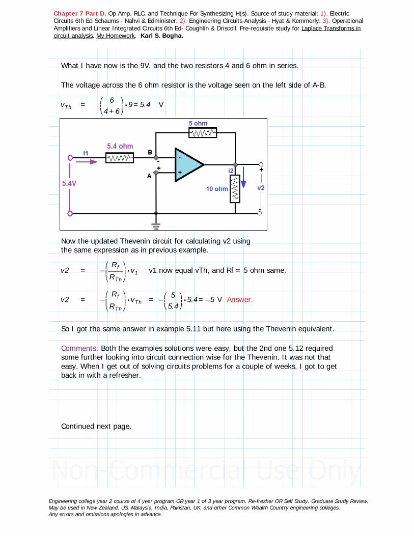
Chapter 7 Part D. Op Amp, RLC, and Technique For Synthesizing H(s). Source of study material: 1). Electric Circuits 6th Ed Schaums - Nahvi & Edminister. 2). Engineering Circuits Analysis - Hyat & Kemmerly. 3). Operational Amplifiers and Linear Integrated Circuits 6th Ed- Coughlin & Driscoll. Pre-requisite study for Laplace Transforms in circuit analysis. My Homework. Karl S. Bogha.
What I have now is the 9V, and the two resistors 4 and 6 ohm in series.
The voltage across the 6 ohm resistor is the voltage seen on the left side of A-B.
vTh = =⋅⎛⎜⎝――
6+4 6⎞⎟⎠
9 5.4 V
Now the updated Thevenin circuit for calculating v2 using the same expression as in previous example.
v2 = ⋅−⎛⎜⎝――Rf
RTh
⎞⎟⎠
v1 v1 now equal vTh, and Rf = 5 ohm same.
v2 = ⋅−⎛⎜⎝――Rf
RTh
⎞⎟⎠
vTh = =⋅−⎛⎜⎝――
55.4⎞⎟⎠
5.4 −5 V Answer.
So I got the same answer in example 5.11 but here using the Thevenin equivalent.
Comments: Both the examples solutions were easy, but the 2nd one 5.12 required some further looking into circuit connection wise for the Thevenin. It was not that easy. When I get out of solving circuits problems for a couple of weeks, I got to get back in with a refresher.
Continued next page.
Engineering college year 2 course of 4 year program OR year 1 of 3 year program. Re-fresher OR Self Study. Graduate Study Review.May be used in New Zealand, US, Malaysia, India, Pakistan, UK, and other Common Wealth Country engineering colleges.Any errors and omissions apologies in advance.

Chapter 7 Part D. Op Amp, RLC, and Technique For Synthesizing H(s). Source of study material: 1). Electric Circuits 6th Ed Schaums - Nahvi & Edminister. 2). Engineering Circuits Analysis - Hyat & Kemmerly. 3). Operational Amplifiers and Linear Integrated Circuits 6th Ed- Coughlin & Driscoll. Pre-requisite study for Laplace Transforms in circuit analysis. My Homework. Karl S. Bogha.
Problem 5.13 Opamp circuit analysis:
Find vC, i1, v2, and Rin (the input resistance seen by the 21V source) in the circuit below.
Solution:
Circuit connections re-worked to show that Rf exist in the circuit.Rest is the same, resistance at opamp terminals infinity, so negligible current flows thru, vA =0, and vB=vA=0V.
So I can use the inverting opamp gain expression for solving v2.But what is vC? Leave it in the expression for now. Next plug it in the sum of currents equation at node C.
Engineering college year 2 course of 4 year program OR year 1 of 3 year program. Re-fresher OR Self Study. Graduate Study Review.May be used in New Zealand, US, Malaysia, India, Pakistan, UK, and other Common Wealth Country engineering colleges.Any errors and omissions apologies in advance.

Chapter 7 Part D. Op Amp, RLC, and Technique For Synthesizing H(s). Source of study material: 1). Electric Circuits 6th Ed Schaums - Nahvi & Edminister. 2). Engineering Circuits Analysis - Hyat & Kemmerly. 3). Operational Amplifiers and Linear Integrated Circuits 6th Ed- Coughlin & Driscoll. Pre-requisite study for Laplace Transforms in circuit analysis. My Homework. Karl S. Bogha.
≔Rf 5000 ≔R1 3000
―v2vC
= −⎛⎜⎝―Rf
R1
⎞⎟⎠
v2 = ⋅−⎛⎜⎝―Rf
R1
⎞⎟⎠
vC
v2 = −⎛⎜⎝――50003000
⎞⎟⎠
vC = −⎛⎜⎝―53⎞⎟⎠
vC
Next we do the KCL at node C:
+++⎛⎜⎝―――−vC 213
⎞⎟⎠⎛⎜⎝――−vC 06⎞⎟⎠⎛⎜⎝―――−vC vD
8⎞⎟⎠⎛⎜⎝――−vC 03⎞⎟⎠
= 0 I can divide all the resistors by 1000 to simplify to reduce to one significant digit.
Note: vD = v2, and v2 = -(5/3)vC.
+++⎛⎜⎝―――−vC 213
⎞⎟⎠⎛⎜⎝――−vC 06⎞⎟⎠⎛⎜⎝―――−vC v28
⎞⎟⎠⎛⎜⎝――−vC 03⎞⎟⎠
= 0
+++⎛⎜⎝―――−vC 213
⎞⎟⎠⎛⎜⎝――−vC 06⎞⎟⎠
⎛⎜⎜⎝―――――−vC⎛⎜⎝−―5
3vC⎞⎟⎠
8
⎞⎟⎟⎠⎛⎜⎝――−vC 03⎞⎟⎠
= 0
Common denominator 24.
⎛⎜⎝――――――――――――
++++−8 vC 168 4 vC 3 vC 5 vC 8 vC
24⎞⎟⎠
= 0 Multiply by 24
⎛⎝ ++++−8 vC 168 4 vC 3 vC 5 vC 8 vC⎞⎠ = 0
−28 vC 168 = 0
vC = 6 V Answer.
v2 = −⎛⎜⎝―53⎞⎟⎠
vC = =−⎛⎜⎝―53⎞⎟⎠
6 −10 V Answer.
i1 :⎛⎜⎝―――−21 vC
3000⎞⎟⎠
≔i1 =⎛⎜⎝―――−21 ((6))
3000⎞⎟⎠
0.005 A = 5 mA Answer.
Engineering college year 2 course of 4 year program OR year 1 of 3 year program. Re-fresher OR Self Study. Graduate Study Review.May be used in New Zealand, US, Malaysia, India, Pakistan, UK, and other Common Wealth Country engineering colleges.Any errors and omissions apologies in advance.
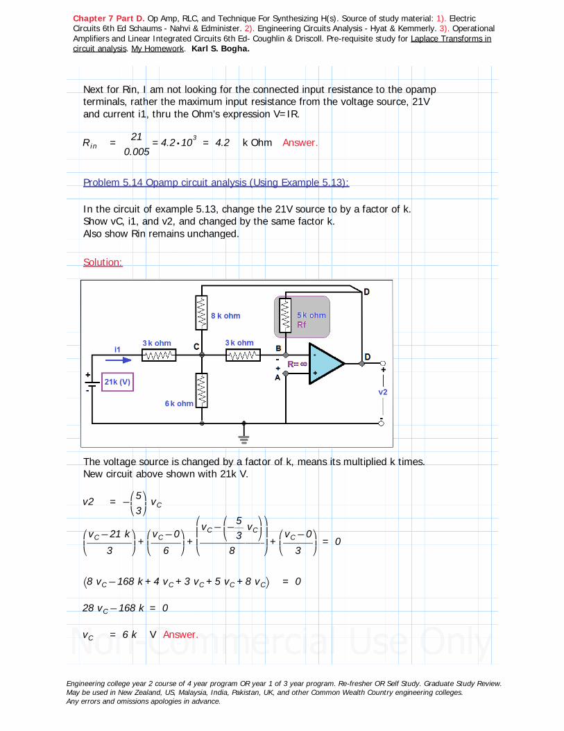
Chapter 7 Part D. Op Amp, RLC, and Technique For Synthesizing H(s). Source of study material: 1). Electric Circuits 6th Ed Schaums - Nahvi & Edminister. 2). Engineering Circuits Analysis - Hyat & Kemmerly. 3). Operational Amplifiers and Linear Integrated Circuits 6th Ed- Coughlin & Driscoll. Pre-requisite study for Laplace Transforms in circuit analysis. My Homework. Karl S. Bogha.
Next for Rin, I am not looking for the connected input resistance to the opamp terminals, rather the maximum input resistance from the voltage source, 21V and current i1, thru the Ohm's expression V=IR.
Rin = =――21
0.005⋅4.2 103 = 4.2 k Ohm Answer.
Problem 5.14 Opamp circuit analysis (Using Example 5.13):
In the circuit of example 5.13, change the 21V source to by a factor of k.Show vC, i1, and v2, and changed by the same factor k.Also show Rin remains unchanged.
Solution:
The voltage source is changed by a factor of k, means its multiplied k times.New circuit above shown with 21k V.
v2 = −⎛⎜⎝―53⎞⎟⎠
vC
+++⎛⎜⎝―――−vC 21 k
3⎞⎟⎠⎛⎜⎝――−vC 06⎞⎟⎠
⎛⎜⎜⎝―――――−vC⎛⎜⎝−―5
3vC⎞⎟⎠
8
⎞⎟⎟⎠⎛⎜⎝――−vC 03⎞⎟⎠
= 0
⎛⎝ ++++−8 vC 168 k 4 vC 3 vC 5 vC 8 vC⎞⎠ = 0
−28 vC 168 k = 0
vC = 6 k V Answer.
Engineering college year 2 course of 4 year program OR year 1 of 3 year program. Re-fresher OR Self Study. Graduate Study Review.May be used in New Zealand, US, Malaysia, India, Pakistan, UK, and other Common Wealth Country engineering colleges.Any errors and omissions apologies in advance.
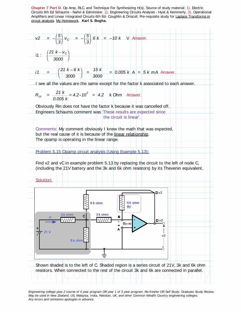
Chapter 7 Part D. Op Amp, RLC, and Technique For Synthesizing H(s). Source of study material: 1). Electric Circuits 6th Ed Schaums - Nahvi & Edminister. 2). Engineering Circuits Analysis - Hyat & Kemmerly. 3). Operational Amplifiers and Linear Integrated Circuits 6th Ed- Coughlin & Driscoll. Pre-requisite study for Laplace Transforms in circuit analysis. My Homework. Karl S. Bogha.
v2 = −⎛⎜⎝―53⎞⎟⎠
vC = −⎛⎜⎝―53⎞⎟⎠
6 k = −10 k V Answer.
i1 :⎛⎜⎝―――
−21 k vC
3000⎞⎟⎠
i1 = ⎛⎜⎝――――
−21 k 6 k3000
⎞⎟⎠
= ――15 k3000
= 0.005 k A = 5 k mA Answer.
I see all the values are the same except for the factor k associated to each answer.
Rin = =―――21 k
0.005 k⋅4.2 103 = 4.2 k Ohm Answer.
Obviously Rin does not have the factor k because it was cancelled off.Engineers Schaums comment was 'These results are expected since the circuit is linear'.
Comments: My comment obviously I knew the math that was expected, but the real cause of it is because of the linear relationship.The opamp is operating in the linear range.
Problem 5.15 Opamp circuit analysis (Using Example 5.13):
Find v2 and vC in example problem 5.13 by replacing the circuit to the left of node C, (including the 21V battery and the 3k and 6k ohm resistors) by its Thevenin equivalent.
Solution:
Shown shaded is to the left of C. Shaded region is a series circuit of 21V, 3k and 6k ohm resistors. When connected to the rest of the circuit 3k and 6k are connected in parallel.
Engineering college year 2 course of 4 year program OR year 1 of 3 year program. Re-fresher OR Self Study. Graduate Study Review.May be used in New Zealand, US, Malaysia, India, Pakistan, UK, and other Common Wealth Country engineering colleges.Any errors and omissions apologies in advance.
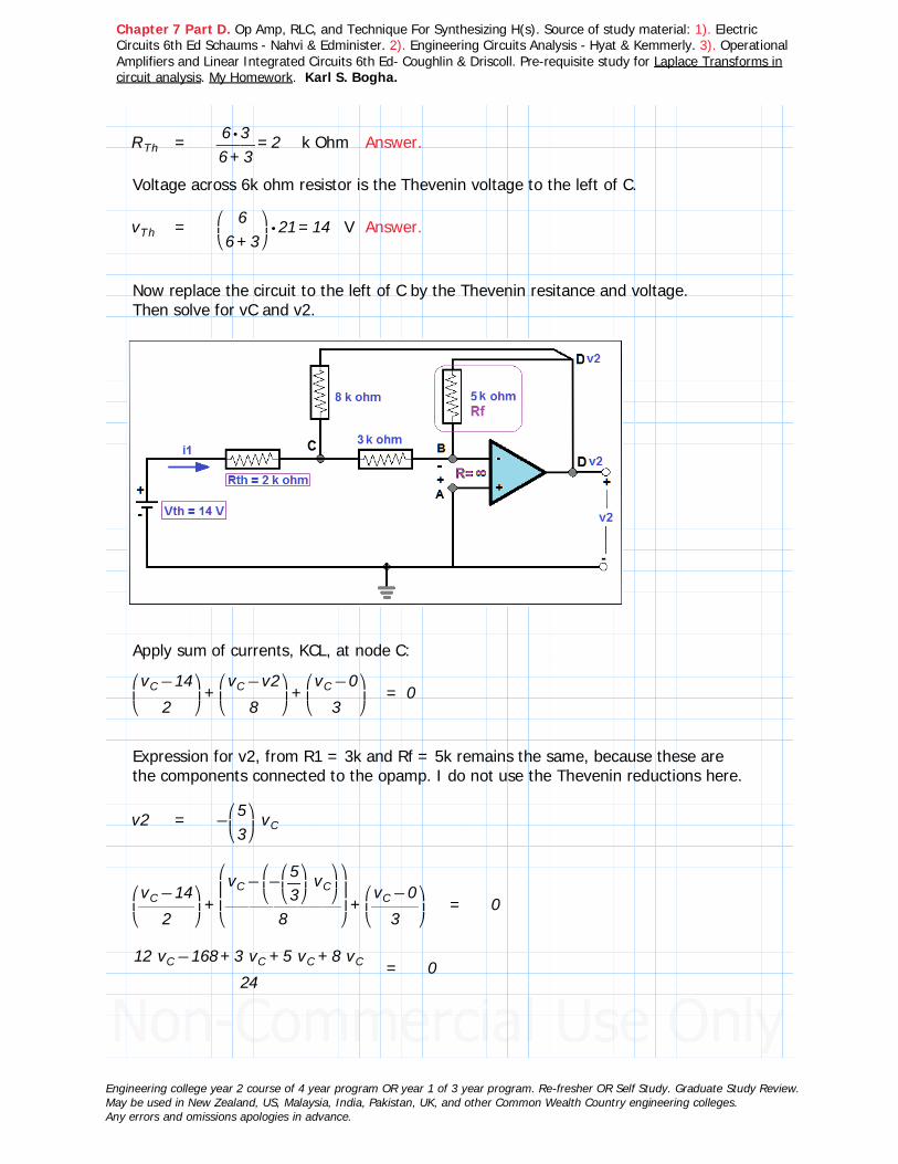
Chapter 7 Part D. Op Amp, RLC, and Technique For Synthesizing H(s). Source of study material: 1). Electric Circuits 6th Ed Schaums - Nahvi & Edminister. 2). Engineering Circuits Analysis - Hyat & Kemmerly. 3). Operational Amplifiers and Linear Integrated Circuits 6th Ed- Coughlin & Driscoll. Pre-requisite study for Laplace Transforms in circuit analysis. My Homework. Karl S. Bogha.
RTh = =――⋅6 3+6 3
2 k Ohm Answer.
Voltage across 6k ohm resistor is the Thevenin voltage to the left of C.
vTh = =⋅⎛⎜⎝――
6+6 3⎞⎟⎠
21 14 V Answer.
Now replace the circuit to the left of C by the Thevenin resitance and voltage.Then solve for vC and v2.
Apply sum of currents, KCL, at node C:
++⎛⎜⎝―――−vC 142
⎞⎟⎠⎛⎜⎝―――−vC v28
⎞⎟⎠⎛⎜⎝――−vC 03⎞⎟⎠
= 0
Expression for v2, from R1 = 3k and Rf = 5k remains the same, because these are the components connected to the opamp. I do not use the Thevenin reductions here.
v2 = −⎛⎜⎝―53⎞⎟⎠
vC
++⎛⎜⎝―――−vC 142
⎞⎟⎠
⎛⎜⎜⎝―――――−vC⎛⎜⎝−⎛⎜⎝―53⎞⎟⎠
vC⎞⎟⎠
8
⎞⎟⎟⎠⎛⎜⎝――−vC 03⎞⎟⎠
= 0
――――――――――+++−12 vC 168 3 vC 5 vC 8 vC
24= 0
Engineering college year 2 course of 4 year program OR year 1 of 3 year program. Re-fresher OR Self Study. Graduate Study Review.May be used in New Zealand, US, Malaysia, India, Pakistan, UK, and other Common Wealth Country engineering colleges.Any errors and omissions apologies in advance.
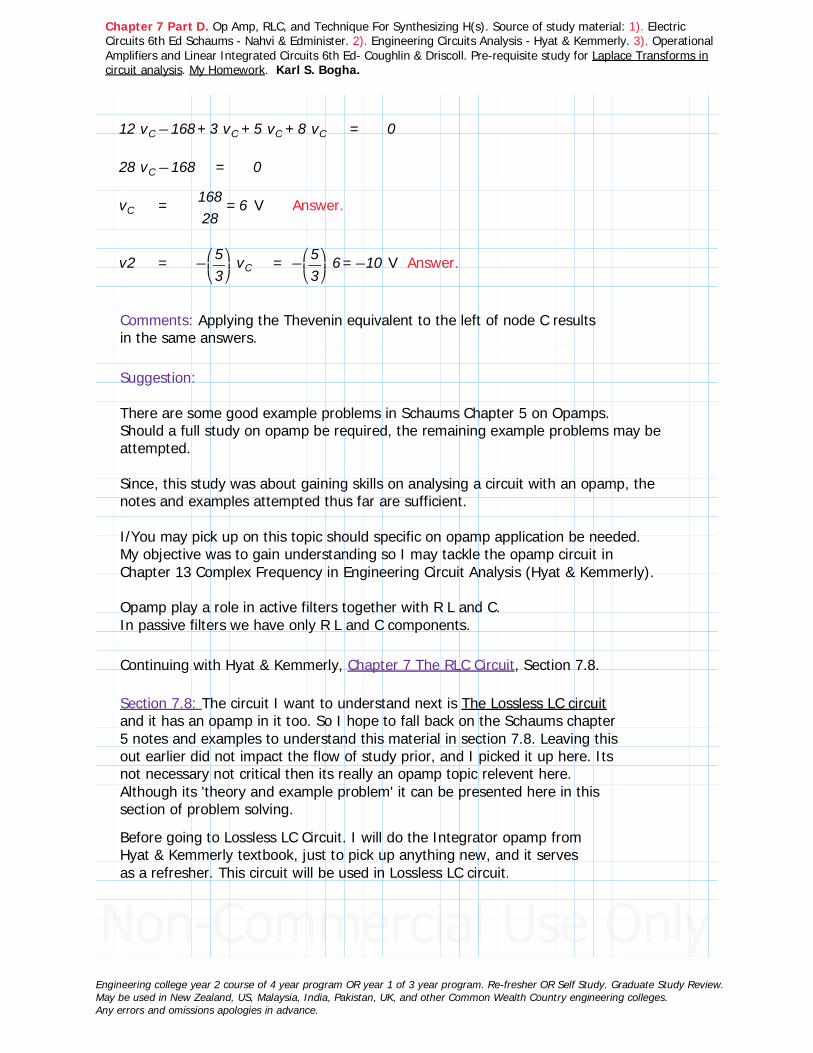
Chapter 7 Part D. Op Amp, RLC, and Technique For Synthesizing H(s). Source of study material: 1). Electric Circuits 6th Ed Schaums - Nahvi & Edminister. 2). Engineering Circuits Analysis - Hyat & Kemmerly. 3). Operational Amplifiers and Linear Integrated Circuits 6th Ed- Coughlin & Driscoll. Pre-requisite study for Laplace Transforms in circuit analysis. My Homework. Karl S. Bogha.
+++−12 vC 168 3 vC 5 vC 8 vC = 0
−28 vC 168 = 0
vC = =――16828
6 V Answer.
v2 = −⎛⎜⎝―53⎞⎟⎠
vC = =−⎛⎜⎝―53⎞⎟⎠
6 −10 V Answer.
Comments: Applying the Thevenin equivalent to the left of node C results in the same answers.
Suggestion:
There are some good example problems in Schaums Chapter 5 on Opamps.Should a full study on opamp be required, the remaining example problems may be attempted.
Since, this study was about gaining skills on analysing a circuit with an opamp, the notes and examples attempted thus far are sufficient.
I/You may pick up on this topic should specific on opamp application be needed.My objective was to gain understanding so I may tackle the opamp circuit in Chapter 13 Complex Frequency in Engineering Circuit Analysis (Hyat & Kemmerly).
Opamp play a role in active filters together with R L and C.In passive filters we have only R L and C components.
Continuing with Hyat & Kemmerly, Chapter 7 The RLC Circuit, Section 7.8.
Section 7.8: The circuit I want to understand next is The Lossless LC circuit and it has an opamp in it too. So I hope to fall back on the Schaums chapter 5 notes and examples to understand this material in section 7.8. Leaving this out earlier did not impact the flow of study prior, and I picked it up here. Its not necessary not critical then its really an opamp topic relevent here. Although its 'theory and example problem' it can be presented here in this section of problem solving.
Before going to Lossless LC Circuit. I will do the Integrator opamp from Hyat & Kemmerly textbook, just to pick up anything new, and it serves as a refresher. This circuit will be used in Lossless LC circuit.
Engineering college year 2 course of 4 year program OR year 1 of 3 year program. Re-fresher OR Self Study. Graduate Study Review.May be used in New Zealand, US, Malaysia, India, Pakistan, UK, and other Common Wealth Country engineering colleges.Any errors and omissions apologies in advance.
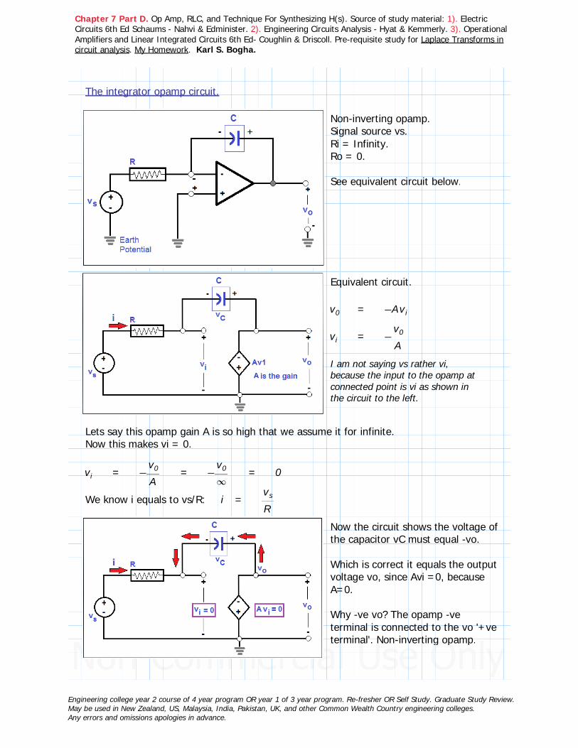
Chapter 7 Part D. Op Amp, RLC, and Technique For Synthesizing H(s). Source of study material: 1). Electric Circuits 6th Ed Schaums - Nahvi & Edminister. 2). Engineering Circuits Analysis - Hyat & Kemmerly. 3). Operational Amplifiers and Linear Integrated Circuits 6th Ed- Coughlin & Driscoll. Pre-requisite study for Laplace Transforms in circuit analysis. My Homework. Karl S. Bogha.
The integrator opamp circuit.
Non-inverting opamp.Signal source vs.Ri = Infinity.Ro = 0.
See equivalent circuit below.
Equivalent circuit.
v0 = −Avi
vi = −―v0
A
I am not saying vs rather vi, because the input to the opamp at connected point is vi as shown in the circuit to the left.
Lets say this opamp gain A is so high that we assume it for infinite.Now this makes vi = 0.
vi = −―v0
A= −―
v0
∞= 0
We know i equals to vs/R: i = ―vs
R
Now the circuit shows the voltage of the capacitor vC must equal -vo.
Which is correct it equals the output voltage vo, since Avi =0, because A=0.
Why -ve vo? The opamp -ve terminal is connected to the vo '+ve terminal'. Non-inverting opamp.
Engineering college year 2 course of 4 year program OR year 1 of 3 year program. Re-fresher OR Self Study. Graduate Study Review.May be used in New Zealand, US, Malaysia, India, Pakistan, UK, and other Common Wealth Country engineering colleges.Any errors and omissions apologies in advance.

Chapter 7 Part D. Op Amp, RLC, and Technique For Synthesizing H(s). Source of study material: 1). Electric Circuits 6th Ed Schaums - Nahvi & Edminister. 2). Engineering Circuits Analysis - Hyat & Kemmerly. 3). Operational Amplifiers and Linear Integrated Circuits 6th Ed- Coughlin & Driscoll. Pre-requisite study for Laplace Transforms in circuit analysis. My Homework. Karl S. Bogha.
vi = 0
vC = −v0
vC = +―1C⌠⌡ d0
t
i t vC ((0)) = −v0 Shown also the initial condition of vC at time t=0, vC(0).
vC = +―1C
⌠⎮⌡
d
0
t
⎛⎜⎝―vs
R⎞⎟⎠
t vC ((0))= −v0
vC = +――1
RC⌠⌡ d0
t
vs t vC ((0)) = −v0 Next multiply by -1.
v0 = −−――1
RC⌠⌡ d0
t
vs t vC ((0))
First term of the output is (1/RC) times the negative of the integral of the input from t=0 to t, and the second term is the negative of the initial value of vC.
If need be the value of (1/RC) can be made equal 1 for example by making R=1 Mohm and C = 1uF. Other selections can be made that will increase or decrease the output voltage. Then we have the negative of the integral and the initial condition of vC(0). OR other values of R and C can be made that will result in a higher or lower value of vo.
The -ve sign of vo is often convenient for engineering system simulations when using the integrator. This -ve sign of course can be changed to positive using a 2nd inverting opamp, as I have seen in the notes for multiple opamp circuit.
v0 = −−――1
RC⌠⌡ d0
t
vs t vC ((0))
The initial condition vC(0) appearing in the expression above can be included by a dc battery and a normally closed switch. See next circuit.
Engineering college year 2 course of 4 year program OR year 1 of 3 year program. Re-fresher OR Self Study. Graduate Study Review.May be used in New Zealand, US, Malaysia, India, Pakistan, UK, and other Common Wealth Country engineering colleges.Any errors and omissions apologies in advance.

Chapter 7 Part D. Op Amp, RLC, and Technique For Synthesizing H(s). Source of study material: 1). Electric Circuits 6th Ed Schaums - Nahvi & Edminister. 2). Engineering Circuits Analysis - Hyat & Kemmerly. 3). Operational Amplifiers and Linear Integrated Circuits 6th Ed- Coughlin & Driscoll. Pre-requisite study for Laplace Transforms in circuit analysis. My Homework. Karl S. Bogha.
For example:
v0 = −−――1
RC⌠⌡ d0
t
vs t vC ((0))
v_battery = 5 VR = 1 MC = 1 uF
−――1
RC= −1
v0 = −−⌠⌡ d0
t
vs t 5 V
NOW lets say this opamp gain A is NOT infinite.Next do a sum of voltage on the equivalent circuit.
The loop is the shaded area.
vs = ++Ri⎛⎜⎝
+―1C⌠⌡ d0
t
i t vC ((0))⎞⎟⎠
v0
+++−vs Ri⎛⎜⎝
+―1C⌠⌡ d0
t
i t vC ((0))⎞⎟⎠
v0 = 0
Current i as usual so far: i = ―――⎛⎝ −vs vi⎞⎠
RSubstitute to eliminate i.
To eliminate vi: v0 = −Avi vi = −―v0
A
Engineering college year 2 course of 4 year program OR year 1 of 3 year program. Re-fresher OR Self Study. Graduate Study Review.May be used in New Zealand, US, Malaysia, India, Pakistan, UK, and other Common Wealth Country engineering colleges.Any errors and omissions apologies in advance.

Chapter 7 Part D. Op Amp, RLC, and Technique For Synthesizing H(s). Source of study material: 1). Electric Circuits 6th Ed Schaums - Nahvi & Edminister. 2). Engineering Circuits Analysis - Hyat & Kemmerly. 3). Operational Amplifiers and Linear Integrated Circuits 6th Ed- Coughlin & Driscoll. Pre-requisite study for Laplace Transforms in circuit analysis. My Homework. Karl S. Bogha.
Substitute i in the expression:
+++−vs ⋅R⎛⎜⎝――−vs vi
R⎞⎟⎠
⎛⎜⎜⎜⎝
+―1C
⌠⎮⌡
d
0
t
⎛⎜⎝――−vs vi
R⎞⎟⎠
t vC ((0))
⎞⎟⎟⎟⎠
v0 = 0
++−+−vs vs vi
⎛⎜⎜⎝
+――1
RC⌠⌡ d0
t
⎛⎝ −vs vi⎞⎠ t vC ((0))⎞⎟⎟⎠
v0 = 0
++−vi
⎛⎜⎜⎝
+――1
RC⌠⌡ d0
t
⎛⎝ −vs vi⎞⎠ t vC ((0))⎞⎟⎟⎠
v0 = 0
Substitute vi in the expression: vi = −―v0
A
++−⎛⎜⎝−―
v0
A⎞⎟⎠
⎛⎜⎜⎜⎝
+――1
RC
⌠⎮⌡
d
0
t
⎛⎜⎝−vs⎛⎜⎝−―
v0
A⎞⎟⎠⎞⎟⎠
t vC ((0))
⎞⎟⎟⎟⎠
v0 = 0
++⎛⎜⎝―v0
A⎞⎟⎠
⎛⎜⎜⎜⎝
+――1
RC
⌠⎮⌡
d
0
t
⎛⎜⎝
+vs ―v0
A⎞⎟⎠
t vC ((0))
⎞⎟⎟⎟⎠
v0 = 0
+v0⎛⎜⎝
+1 ―1A⎞⎟⎠
⎛⎜⎜⎜⎝
+――1
RC
⌠⎮⌡
d
0
t
⎛⎜⎝
+vs ―v0
A⎞⎟⎠
t vC ((0))
⎞⎟⎟⎟⎠
= 0
v0⎛⎜⎝
+1 ―1A⎞⎟⎠
= −−――1
RC
⌠⎮⌡
d
0
t
⎛⎜⎝
+vs ―v0
A⎞⎟⎠
t vC ((0)) Correct.
The above expression is when A is NOT equal to infinity.
Returning to when A approaches infinity:
v0⎛⎜⎝
+1 ―1∞⎞⎟⎠
= −−――1
RC
⌠⎮⌡
d
0
t
⎛⎜⎝
+vs ―v0
∞⎞⎟⎠
t vC ((0))
v0 = −−――1
RC⌠⌡ d0
t
⎛⎝vs⎞⎠ t vC ((0)) Just as we had early on when A was set equal to infinity.
Engineering college year 2 course of 4 year program OR year 1 of 3 year program. Re-fresher OR Self Study. Graduate Study Review.May be used in New Zealand, US, Malaysia, India, Pakistan, UK, and other Common Wealth Country engineering colleges.Any errors and omissions apologies in advance.

Chapter 7 Part D. Op Amp, RLC, and Technique For Synthesizing H(s). Source of study material: 1). Electric Circuits 6th Ed Schaums - Nahvi & Edminister. 2). Engineering Circuits Analysis - Hyat & Kemmerly. 3). Operational Amplifiers and Linear Integrated Circuits 6th Ed- Coughlin & Driscoll. Pre-requisite study for Laplace Transforms in circuit analysis. My Homework. Karl S. Bogha.
Completed the integrator opamp, which I dont remember doing it exactly like Schaums, here in Hyat & Kemmerly we do both A = infinity and also the additional part when A is NOT equal infinity. So some difference was there.
The differentiator circuit can be built and as shown in the Schaums notes, similarly said here this circuit is not parctical due to size, weight, cost, and associated resistance and capacitance.
Continued next page to Lossless LC circuit.
Engineering college year 2 course of 4 year program OR year 1 of 3 year program. Re-fresher OR Self Study. Graduate Study Review.May be used in New Zealand, US, Malaysia, India, Pakistan, UK, and other Common Wealth Country engineering colleges.Any errors and omissions apologies in advance.

Chapter 7 Part D. Op Amp, RLC, and Technique For Synthesizing H(s). Source of study material: 1). Electric Circuits 6th Ed Schaums - Nahvi & Edminister. 2). Engineering Circuits Analysis - Hyat & Kemmerly. 3). Operational Amplifiers and Linear Integrated Circuits 6th Ed- Coughlin & Driscoll. Pre-requisite study for Laplace Transforms in circuit analysis. My Homework. Karl S. Bogha.
Section 7-8 The Lossless LC circuit - Hyat & Kemmerly.
So the circuit from RLC goes to LC when R goes to infinity.
How does the LC circuit perform then?
Engineers said we have an LC loop in which an oscillatory response can be maintained forever.
Engineers: Let us look briefly at an example of such a circuit, and then discuss another means of obtaining an identical response without the need of supplying any inductance.
The 'another means' in the sentence above is thru the use of an opamp and resistors using the integrator circuit.
Given the following for the circuit to the left, keeping it simple:
L = 4 H C = ⎛⎜⎝―1
36⎞⎟⎠
F
i ((0)) = −―16
A v ((0)) = 0
Circuit is source free thus: α = 0ω0
2 = 9ωd = ω = 3
Engineering college year 2 course of 4 year program OR year 1 of 3 year program. Re-fresher OR Self Study. Graduate Study Review.May be used in New Zealand, US, Malaysia, India, Pakistan, UK, and other Common Wealth Country engineering colleges.Any errors and omissions apologies in advance.

Chapter 7 Part D. Op Amp, RLC, and Technique For Synthesizing H(s). Source of study material: 1). Electric Circuits 6th Ed Schaums - Nahvi & Edminister. 2). Engineering Circuits Analysis - Hyat & Kemmerly. 3). Operational Amplifiers and Linear Integrated Circuits 6th Ed- Coughlin & Driscoll. Pre-requisite study for Laplace Transforms in circuit analysis. My Homework. Karl S. Bogha.
Condition: Alpha < Omega: ie 0<3.
Underdamped case.
The function expression typical is from RLC notes:
fn ((t)) = ⋅e−αt ⎛⎝ +Acos ⎛⎝ωdt⎞⎠ Bsin ⎛⎝ωdt⎞⎠⎞⎠
Since alpha = 0.
fn ((t)) = ⋅e−0 t ⎛⎝ +Acos ⎛⎝ωdt⎞⎠ Bsin ⎛⎝ωdt⎞⎠⎞⎠
fn ((t)) = +Acos ⎛⎝ωdt⎞⎠ Bsin ⎛⎝ωdt⎞⎠
Since ωd = 3
fn ((t)) = +Acos ((3 t)) Bsin ((3 t))
v ((t)) = +Acos ((3 t)) Bsin ((3 t)) This is the voltage of the circuit, based on the values of alpha and omega, across the inductor L and capacitor C.
v ((0)) = 0 At time t voltage v = 0, the initial condition we were given.
v ((0)) = +⋅A cos ((0)) ⋅B sin ((0)) = +⋅A 1 ⋅B 0v ((0)) = AA = 0 When voltage = 0, at time t=0.
v ((t)) = +Acos ((3 t)) Bsin ((3 t)) Continue with the diferentiation of the voltage expression.
――dv ((t))
dt= +−3 Asin ((3 t)) 3 Bcos ((3 t))
At t=0 ――dv ((t))
dt= +−3 Asin ((0)) 3 Bcos ((0)) = +⋅−3 A 0 ⋅3 B 1 = 3 B
We have an LC circuit, the expression for vC is (1/C) integral of i. We are given i(0) = - 1/6A. So lets use the capacitor equation for voltage since its got the current value in it. dv/dt will have per sec, so dv/dt = 3B/s.
At t=0 ――dv ((t))
dt= 3 ―
Bs
vC ((0)) = ―1C⌠⌡ d0
t
i t
The value of i(t) at t = 0 ? - (1/6) A.―――dvC ((t))
dt= ―
1C
i ((t)) = ―1C
i ((0))
Engineering college year 2 course of 4 year program OR year 1 of 3 year program. Re-fresher OR Self Study. Graduate Study Review.May be used in New Zealand, US, Malaysia, India, Pakistan, UK, and other Common Wealth Country engineering colleges.Any errors and omissions apologies in advance.
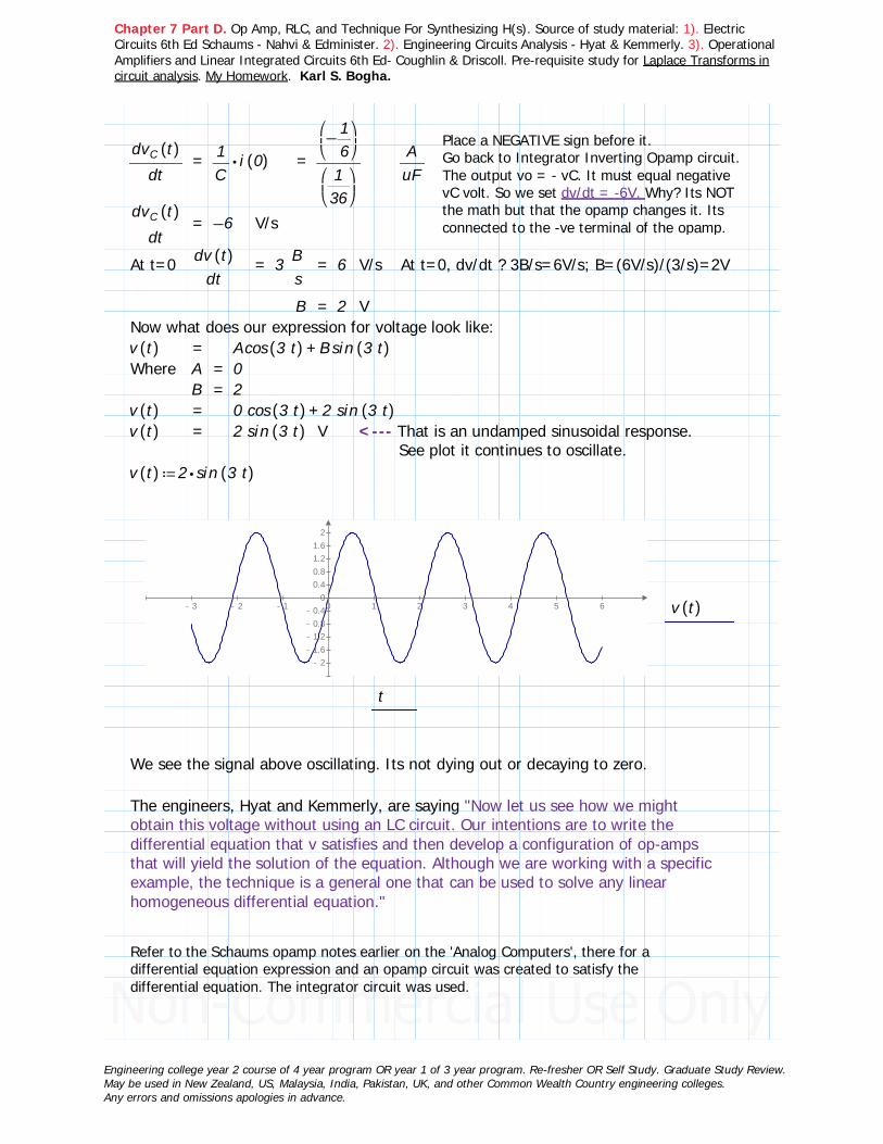
Chapter 7 Part D. Op Amp, RLC, and Technique For Synthesizing H(s). Source of study material: 1). Electric Circuits 6th Ed Schaums - Nahvi & Edminister. 2). Engineering Circuits Analysis - Hyat & Kemmerly. 3). Operational Amplifiers and Linear Integrated Circuits 6th Ed- Coughlin & Driscoll. Pre-requisite study for Laplace Transforms in circuit analysis. My Homework. Karl S. Bogha.
Place a NEGATIVE sign before it. Go back to Integrator Inverting Opamp circuit. The output vo = - vC. It must equal negative vC volt. So we set dv/dt = -6V. Why? Its NOT the math but that the opamp changes it. Its connected to the -ve terminal of the opamp.
―――dvC ((t))
dt= ⋅―
1C
i ((0)) = ――
⎛⎜⎝−―1
6⎞⎟⎠
⎛⎜⎝―136⎞⎟⎠
――A
uF
―――dvC ((t))
dt= −6 V/s
At t=0 ――dv ((t))
dt= 3 ―
Bs
= 6 V/s At t=0, dv/dt ? 3B/s=6V/s; B=(6V/s)/(3/s)=2V
B = 2 VNow what does our expression for voltage look like:v ((t)) = +Acos ((3 t)) Bsin ((3 t))Where A = 0
B = 2v ((t)) = +0 cos ((3 t)) 2 sin ((3 t))v ((t)) = 2 sin ((3 t)) V <--- That is an undamped sinusoidal response.
See plot it continues to oscillate.≔v ((t)) ⋅2 sin ((3 t))
-1.2-0.8-0.4
00.40.81.21.6
-2-1.6
2
-1 0 1 2 3 4 5-3 -2 6
t
v ((t))
We see the signal above oscillating. Its not dying out or decaying to zero.
The engineers, Hyat and Kemmerly, are saying "Now let us see how we might obtain this voltage without using an LC circuit. Our intentions are to write the differential equation that v satisfies and then develop a configuration of op-amps that will yield the solution of the equation. Although we are working with a specific example, the technique is a general one that can be used to solve any linear homogeneous differential equation."
Refer to the Schaums opamp notes earlier on the 'Analog Computers', there for a differential equation expression and an opamp circuit was created to satisfy the differential equation. The integrator circuit was used.
Engineering college year 2 course of 4 year program OR year 1 of 3 year program. Re-fresher OR Self Study. Graduate Study Review.May be used in New Zealand, US, Malaysia, India, Pakistan, UK, and other Common Wealth Country engineering colleges.Any errors and omissions apologies in advance.

Chapter 7 Part D. Op Amp, RLC, and Technique For Synthesizing H(s). Source of study material: 1). Electric Circuits 6th Ed Schaums - Nahvi & Edminister. 2). Engineering Circuits Analysis - Hyat & Kemmerly. 3). Operational Amplifiers and Linear Integrated Circuits 6th Ed- Coughlin & Driscoll. Pre-requisite study for Laplace Transforms in circuit analysis. My Homework. Karl S. Bogha.
We place a node for the zero 0V reference. Current shown going downward for L, and for C the current is flowing out of the +ve terminal upward.Now we can do a sum of currents at the node. Which is I_L + I_C = 0.Or I_L = - I_C.
+iL iC = 0
+―1L⌠⌡ d0
t
v t ⋅C ――dvC
dt= 0
I can set the voltage integral equal v. In a series circuit here, the source of voltage is the capacitor. Capacitor is also the source of current. The inductor creates a magnetic field, generates a current and passes it on to the capacitor, that keeps the capacitor going. Emm? Thats what they meant a lossless LC circuit. You verify.
―1L⌠⌡ d0
t
v t = ―14⌠⌡ d0
t
v t
⋅C ――dvC
dt= 'Current at time t=0' + 'current expression for time t>0'.
= +i ((0)) ⎛⎜⎝―1
36⎞⎟⎠――dv ((t))
dt
⋅C ――dvC
dt= +−―
16
⋅⎛⎜⎝―1
36⎞⎟⎠―dvdt
+iL iC = +−―14⌠⌡ d0
t
v t ―16
⋅⎛⎜⎝―1
36⎞⎟⎠―dvdt
= 0 <--- Differentiate this expression
Differentiating the expression above once, gives me the d2v/dt2 term, results in the 2nd order differential term. Which is the 2nd order term in the opamp study I did I know it plays a role in building the circuit.
d2t/dt2 is ---> ――d2 v
dt2<---2nd order differential term
Next lets differentiate to get the 2nd order term.
Engineering college year 2 course of 4 year program OR year 1 of 3 year program. Re-fresher OR Self Study. Graduate Study Review.May be used in New Zealand, US, Malaysia, India, Pakistan, UK, and other Common Wealth Country engineering colleges.Any errors and omissions apologies in advance.

Chapter 7 Part D. Op Amp, RLC, and Technique For Synthesizing H(s). Source of study material: 1). Electric Circuits 6th Ed Schaums - Nahvi & Edminister. 2). Engineering Circuits Analysis - Hyat & Kemmerly. 3). Operational Amplifiers and Linear Integrated Circuits 6th Ed- Coughlin & Driscoll. Pre-requisite study for Laplace Transforms in circuit analysis. My Homework. Karl S. Bogha.
Differentiating the first term removes the integral.+―14
v ⋅⎛⎜⎝―1
36⎞⎟⎠――d2 v
dt2= 0
⋅⎛⎜⎝―1
36⎞⎟⎠――d2 v
dt2= −―
14
v
――d2 v
dt2= ⋅−⎛⎜⎝
―v4⎞⎟⎠
36
The unit on the RHS will be volt/s^2 because the derivative being taken on the LHS is of voltage. Since v is an expression equal to 2 sin(3t)V it can be left as v.
――d2 v
dt2= −9 v
Next the application of the opamp as an integrator twice, to solve the differential equation d2v/dt2 = 9v.
Comment: I can see, already its a difficult task for me. The Engineers have written a few words and given the circuit, so I have to stay close to their wording, and not attempt to look original giving the impression I knew something more about it.
Since its a new technique to solve this problem, I will number the steps to make it easier to follow.
Step 1.
Assume the highest order derivative appearing in the differential equation here is d2v/dt2 and it is available at some point in our configuration of opamps. Lets say that some point is at an arbitary point A.
Arbitary means simply based on a random choice without any technical or personal preference to it.
I found:―dvdt
= 6 V/s ――d2 v
dt2= −9 v Use the integrator with RC = 1.
Makes things easier to start with.
Integrator: That means the input must be d2v/dt2 and so the output is -dv/dt.Using the non-inverting opamp the output will be -ve, so -dv/dt.
Therefore, a condition was placed the integration result's in a sign change.
Engineering college year 2 course of 4 year program OR year 1 of 3 year program. Re-fresher OR Self Study. Graduate Study Review.May be used in New Zealand, US, Malaysia, India, Pakistan, UK, and other Common Wealth Country engineering colleges.Any errors and omissions apologies in advance.

Chapter 7 Part D. Op Amp, RLC, and Technique For Synthesizing H(s). Source of study material: 1). Electric Circuits 6th Ed Schaums - Nahvi & Edminister. 2). Engineering Circuits Analysis - Hyat & Kemmerly. 3). Operational Amplifiers and Linear Integrated Circuits 6th Ed- Coughlin & Driscoll. Pre-requisite study for Laplace Transforms in circuit analysis. My Homework. Karl S. Bogha.
Step 2.
The value of dv/dt equal: 6 V/s I set the -6V in the integrator opamp circuit.
Initial value of dv/dt: −6 V/s
Circuit shown here is the first stage output is -6V.
R and C values of 1M ohm and 1uF.
DC battery value of 6V.
What is the voltage at the node just past R=1 Mohm? Its zero volts. Because the 1Mohm does not permit appreciable current flow. Assume zero current. That solves where -9V went, its the volt drop across R=1Mohm. The 6V battery takes the circuit further.
Step 3.
Next the -6V becomes the input to the 2nd integrator opamp.Since the next circuit configuration is an integrator, the input dv/dt will result in the output v(t) or v. Correct. What about the initial value for this part ?At t=0, v(0) = 0V. Hence the dc battery value is 0V, no battery.See circuit below, with R and C the same values in 2nd opamp. No dc battery.
Engineering college year 2 course of 4 year program OR year 1 of 3 year program. Re-fresher OR Self Study. Graduate Study Review.May be used in New Zealand, US, Malaysia, India, Pakistan, UK, and other Common Wealth Country engineering colleges.Any errors and omissions apologies in advance.

Chapter 7 Part D. Op Amp, RLC, and Technique For Synthesizing H(s). Source of study material: 1). Electric Circuits 6th Ed Schaums - Nahvi & Edminister. 2). Engineering Circuits Analysis - Hyat & Kemmerly. 3). Operational Amplifiers and Linear Integrated Circuits 6th Ed- Coughlin & Driscoll. Pre-requisite study for Laplace Transforms in circuit analysis. My Homework. Karl S. Bogha.
The output of opamp 2 is v(t) or v, which is actually the signal v = 2 sin(3t) V.
That solves v(t).
d2v/dt2 was solved for -9v at the input of opamp 1.
So to do that we have a feedback connection from opamp 2 to 3, and from 3 to opamp 1 back to point A.
Step 4.
――d2 v
dt2= −9v The signal out of opamp 2 is the same signal going into opamp
3 which is v, ie v=2sin(3t), with the purpose of solving for -9v The need is to create an amplification 9 times of v, and the output with a negative sign, so it becomes -9v.
Gain A = −――RfR
= ―v0
vi<---Inverting opamp expression has negative sign on gain.
―――−90 k10 k
= ―v0
vThus v0 = −9 v
To get a gain of 9, make Rf = 90 kohm and R = 10 kohm.To get the -ve sign on the gain use an inverting opamp.
Gain A = −――RfR
= =−―9010
−9
Opamp 3 solves for -9v, which is 9(2 sin(3t)) = 18 sin (3t).
−9 v = −9 ((2 sin ((3 t)))) = −18 sin ((3 t))
Engineering college year 2 course of 4 year program OR year 1 of 3 year program. Re-fresher OR Self Study. Graduate Study Review.May be used in New Zealand, US, Malaysia, India, Pakistan, UK, and other Common Wealth Country engineering colleges.Any errors and omissions apologies in advance.

Chapter 7 Part D. Op Amp, RLC, and Technique For Synthesizing H(s). Source of study material: 1). Electric Circuits 6th Ed Schaums - Nahvi & Edminister. 2). Engineering Circuits Analysis - Hyat & Kemmerly. 3). Operational Amplifiers and Linear Integrated Circuits 6th Ed- Coughlin & Driscoll. Pre-requisite study for Laplace Transforms in circuit analysis. My Homework. Karl S. Bogha.
When we integrate -18 sin 3(t): ⌠⌡ d0
t
18 sin ((3 t)) t = −―183
cos ((3 t))
= −6 cos ((3 t))
At time t=0 −6 cos ((3 t)) becomes: −6 cos ((0)) = −6 = −6VIntegrating a voltage expression would result in the unit of voltage V.
Which the output of opamp 1 is -6V.This was achieved by setting a dc battery equal 6V in the inverting opamp 1 circuit.The inverting opamp results in -6V. Its negative 6 Volts.
The full circuit shown below.
The circuit comes on with the first switch closing at t=0, and the two integrator opamp switches opening at t=0. The integrator opamp 1 switch open after C is charged to 6V at t=0, and switch 2 on opamp 2 opens at t=0 with the capacitor C charging up v(t). The signal v or v(t) contines to opamp 3 where its amplified 9 times, and returns to the input of opamp 1 resistor 1 Mohm as -9v. Thats the lossless circuit theoretically.
The circuit's output at opamp 2 ? The undamped sinusoidal signal v = 2 sin (3t).
Engineering college year 2 course of 4 year program OR year 1 of 3 year program. Re-fresher OR Self Study. Graduate Study Review.May be used in New Zealand, US, Malaysia, India, Pakistan, UK, and other Common Wealth Country engineering colleges.Any errors and omissions apologies in advance.

Chapter 7 Part D. Op Amp, RLC, and Technique For Synthesizing H(s). Source of study material: 1). Electric Circuits 6th Ed Schaums - Nahvi & Edminister. 2). Engineering Circuits Analysis - Hyat & Kemmerly. 3). Operational Amplifiers and Linear Integrated Circuits 6th Ed- Coughlin & Driscoll. Pre-requisite study for Laplace Transforms in circuit analysis. My Homework. Karl S. Bogha.
Conclusion: Both the LC circuit and the opamp circuit, shown above, have the same output. However, the opamp circuit does not contain a single inductor. It simply acts as though it contained an inductor, providing the appropriate sinusoidal voltage between its output terminal and earth/ground. This is considered a practical or economic advantage in the circuit design.
Sure lots and lots of problems can be done for opamp. Multitudes.
So, of course I have a cut-off line here.
Next 4:
I get back on Section 13-8 A Technique for synthesizing the voltage ratio H(s) = Vout / Vin.
I left it to pick up on opamps so I may tackle the opamp circuits in Section 13-8.However, it is worth the time and effort to gain opamp skills.
Engineering college year 2 course of 4 year program OR year 1 of 3 year program. Re-fresher OR Self Study. Graduate Study Review.May be used in New Zealand, US, Malaysia, India, Pakistan, UK, and other Common Wealth Country engineering colleges.Any errors and omissions apologies in advance.

Chapter 7 Part 3D. Op Amp, RLC, and Technique For Synthesizing H(s). Source of study material: 1). Electric Circuits 6th Ed Schaums - Nahvi & Edminister. 2). Engineering Circuits Analysis - Hyat & Kemmerly. 3). Operational Amplifiers and Linear Integrated Circuits 6th Ed- Coughlin & Driscoll. Pre-requisite study for Laplace Transforms in circuit analysis. My Homework. Karl S. Bogha.
Part 3 D: Section 4.
RLC Higher Order Circuits - Continuing From Part 3B.
1. Engineering Circuit Analysis Hyat and Kemmerly 4th Edition: Section 13-8: A Technique For Synthesizing The Voltage Ratio H(s) = Vout / Vin.
2. Schaums: Magnitude scaling
3. Schaums: Frequency scaling
4. Schaums: Higher order active circuits
Relevant 'partially solved examples, problems and supplementary problems' were solved. Electric Circuits textbooks have additional problems which can be worked on as required.
This completes the prerequisite studies for Laplace Transforms In Circuit Analysis. It was my intention to work Schaums Electric Circuits supplementary textbook, and Engineering Circuit Analysis main textbook. A few other textbooks were used.
What Next?
You can be a student at college so you plan on successfully completing the circuits course and then into year 3 courses.
Others:
A. You may be a graduate student who need to study RLC circuits course for a specific course prerequisite.
B. You may be an engineer who need to study this topic for work or exams because its been several years ago since you first studied it.
Apologies for any errors and omissions.
Engineering college year 2 course of 4 year program OR year 1 of 3 year program. Re-fresher OR Self Study. Graduate Study Review.May be used in New Zealand, US, Malaysia, India, Pakistan, UK, and other Common Wealth Country engineering colleges.Any errors and omissions apologies in advance.

Chapter 7 Part D. Op Amp, RLC, and Technique For Synthesizing H(s). Source of study material: 1). Electric Circuits 6th Ed Schaums - Nahvi & Edminister. 2). Engineering Circuits Analysis - Hyat & Kemmerly. 3). Operational Amplifiers and Linear Integrated Circuits 6th Ed- Coughlin & Driscoll. Pre-requisite study for Laplace Transforms in circuit analysis. My Homework. Karl S. Bogha.
Section 4.
Textbook: Engineering Circuit Analysis - Hyat & Kemmerly
Continuation from Part 3C: Section 13-7 Natural response and the s plane
To
Part 3D: Section 13-8 A Technique for synthesizing the voltage ratio H(s) = Vout / Vin.
13-8 A technique for synthesizing the voltage ratio H(s) = Vout / Vin.
So far for the Hyat Kemmerly Engineering Circuit Analysis textbook the discussion and presentation of skills has been around:1. poles and zeros2. expressing transfer functions using poles and zeros as - ratios of factors OR - polynomials in s,3. calculated forced responses from poles and zeros4. used the poles to establish the form of the natural response
Now the need is to 'determine a network' that can provide a desired transfer function.What is the network? The electric circuit.What is the desired function? The transfer function.
So given a transfer function can an electric circuit be created?This is the topic here. It is at a higher level, requires use of mathematics, and electric circuit principles.Here to keep things simple, H(s) is restricted to critical frequencies on the negative sigma axis and including the origin.s = +σ jωσ : On the negative side of the sigma axis,
including the origin.Example of such a transfer function:
H ((s)) = ―――(( +s 3))
(( +s 10))
Pole: sp = −10 Zero: sz = −3

Chapter 7 Part D. Op Amp, RLC, and Technique For Synthesizing H(s). Source of study material: 1). Electric Circuits 6th Ed Schaums - Nahvi & Edminister. 2). Engineering Circuits Analysis - Hyat & Kemmerly. 3). Operational Amplifiers and Linear Integrated Circuits 6th Ed- Coughlin & Driscoll. Pre-requisite study for Laplace Transforms in circuit analysis. My Homework. Karl S. Bogha.
A few examples of what was meant on the -ve side of the sigma axis:
H1 ((s)) = ――――10 (( +s 2))
(( +s 5))H2 ((s)) = ―――
−5 s
(( +s 8))2
H3 ((s)) = 0.1 s (( +s 2))
Lets say we have a network, one end I have the Vin, the other end the Vout. The network is an ideal opamp.So, I were to find the voltage gain it would be something I had done in the previous sections. Which is Vout/vin.
Given:
H ((s)) = ――Vout
Vin
Find the network?ORForm the network?
Synthesizing means to create something new from other existing parts.Here we got a transfer function, and we want to create the network that satisfies the transfer function. Obviously the parts in the network, electrical components, will have to work at satisfying the end result which here is the transfer function.
Lets start with the ideal opamp.
K Current LAW at -ve terminal:
+――Vin
z1――Vout
zf= 0
――Vout
Zf= −――
Vin
Z1
Gain ――Vout
Vin= −――Zf
Z1
When Z1 and Zf are both resistances, the circuit acts as an inverting amplifier. Its either an amplifier or attenuator. Attenuator would be a low amplification, including made lower than original signal, compared to amplifier that increases. In this case its quite simple, I completed a few circuits with both impedances Z1 and Zf being resistors.

Chapter 7 Part D. Op Amp, RLC, and Technique For Synthesizing H(s). Source of study material: 1). Electric Circuits 6th Ed Schaums - Nahvi & Edminister. 2). Engineering Circuits Analysis - Hyat & Kemmerly. 3). Operational Amplifiers and Linear Integrated Circuits 6th Ed- Coughlin & Driscoll. Pre-requisite study for Laplace Transforms in circuit analysis. My Homework. Karl S. Bogha.
Situation is this: The skill I have to gain here is when one of the impedances Z1 or Zf is a resistor and the other a RC network.
To keep it simple and low level, the previous opamp circuit with impedances Z1 and Z2 will be used.
I have 2 circuits. I identify them as opamp 1 and opamp 2 circuits.Provided below. Their similarities and differences easily seen.
Opamp 1 circuit:
Z1 = R1
Zf = ――――⋅Rf ⎛⎜⎝――1sCf⎞⎟⎠
+Rf ⎛⎜⎝――1sCf⎞⎟⎠
In the s - domain. In Part 3C there were several examples on finding the transfer functions H(s), given a circuit.
Simplify Zf, first multiply by sCf:
Zf = ――――Rf
+⋅Rf sCf 1= ――――Rf
+1 ⋅Rf sCfNext divide by RfCf.
Zf = ――――――1Cf
+――1RfCf
s

Chapter 7 Part D. Op Amp, RLC, and Technique For Synthesizing H(s). Source of study material: 1). Electric Circuits 6th Ed Schaums - Nahvi & Edminister. 2). Engineering Circuits Analysis - Hyat & Kemmerly. 3). Operational Amplifiers and Linear Integrated Circuits 6th Ed- Coughlin & Driscoll. Pre-requisite study for Laplace Transforms in circuit analysis. My Homework. Karl S. Bogha.
That sorts Zf, rearranged with s infront. In that Engineer/Mathematician form of expression!
Zf = ――――――1Cf
+――1RfCf
s= ――――
――1Cf
+s ――1RfCf
Next for the gain expression:
H ((s)) = ――Vout
Vin= −――
ZfZ1
Leave it here.Good to go!
−――ZfZ1
= −――――
⎛⎜⎜⎜⎝
――――――1Cf
+s ――1RfCf
⎞⎟⎟⎟⎠
R1= −――――
――1R1Cf
⎛⎜⎝
+s ――1RfCf
⎞⎟⎠
H1 ((s)) = −――――――1R1Cf
⎛⎜⎝
+s ――1RfCf
⎞⎟⎠
Transfer function for opamp #1 circuit.With s isolated to provide a critical frequency.
By studying the transfer function above there is only a single finite critical frequrency that is the pole, and there is no zero frequency. The pole is:
sp = −⎛⎜⎝――
1RfCf
⎞⎟⎠
Next for opamp 2 circuit:
Almost a swap for Z1 and Zf in circuit 1 but the component values are different.
Z1 = ――――⋅R1 ⎛⎜⎝――1sC1⎞⎟⎠
+R1 ⎛⎜⎝――1sC1⎞⎟⎠
Zf = Rf
I can reuse the expression results from circuit 1 with a little modification.

Chapter 7 Part D. Op Amp, RLC, and Technique For Synthesizing H(s). Source of study material: 1). Electric Circuits 6th Ed Schaums - Nahvi & Edminister. 2). Engineering Circuits Analysis - Hyat & Kemmerly. 3). Operational Amplifiers and Linear Integrated Circuits 6th Ed- Coughlin & Driscoll. Pre-requisite study for Laplace Transforms in circuit analysis. My Homework. Karl S. Bogha.
That sorts Z1. In that Engineer/Mathematician form of expression!Z1 = ――――
⋅R1 ⎛⎜⎝――1sC1⎞⎟⎠
+R1 ⎛⎜⎝――1sC1⎞⎟⎠
= ――――――1C1
+s ――1R1C1
H ((s)) = ――Vout
Vin= −――
ZfZ1
= −――――Rf
⎛⎜⎜⎜⎝
――――――1C1
+s ――1R1C1
⎞⎟⎟⎟⎠
−――ZfZ1
= ⋅−Rf
⎛⎜⎜⎜⎝
――――+s ――1
R1C1
――1C1
⎞⎟⎟⎟⎠
Inverting the bottom expression.
Multiply by C1 top and bottom.−――
ZfZ1
= −
⎛⎜⎜⎜⎝
――――+Rfs ――Rf
R1C1
――1C1
⎞⎟⎟⎟⎠
−――ZfZ1
= +−((RfC1s)) ――RfR1
Correct.
Engineer wants in that form which is more beneficial/practical for this circuit.Make it to where both terms are almost similar. More pleasing? Yes.
−――ZfZ1
= −Rf ⎛⎜⎝+C1s ――
1R1⎞⎟⎠
To make both terms with R and C?Little rearrangement and multiply by fraction term by 1/C1.
−――ZfZ1
= −RfC1 ⎛⎜⎝+s ――
1R1C1
⎞⎟⎠
Better and I have s isolated for a critical frequency. Thats why!
H2 ((s)) = −RfC1 ⎛⎜⎝+s ――
1R1C1
⎞⎟⎠
Transfer function for opamp #2 circuit.With s isolated to provide a critical frequency.
By studying the transfer function above there is only a single finite critical frequrency that is the zero, and there is no pole frequency. The zero is:
sz = −⎛⎜⎝――
1R1C1
⎞⎟⎠
Little success here got 2 transfer expression sorted.

Chapter 7 Part D. Op Amp, RLC, and Technique For Synthesizing H(s). Source of study material: 1). Electric Circuits 6th Ed Schaums - Nahvi & Edminister. 2). Engineering Circuits Analysis - Hyat & Kemmerly. 3). Operational Amplifiers and Linear Integrated Circuits 6th Ed- Coughlin & Driscoll. Pre-requisite study for Laplace Transforms in circuit analysis. My Homework. Karl S. Bogha.
In the early opamp studies, we know the transfer function is NOT dependent on the load impedance. Shown in the circuit to the left impedance load ZL.
In other words, putting it in electrical language:'For our ideal opamps, the output for Thevenin impedance is zero and therefore Vout and Vout/Vin are NOT functions of any load ZL that may be placed across the output terminals. This includes the input to another opamp' - Hyat & Kemmerly.
'Therefore, we may connect circuits having poles and zeros at specified locations in cascade, where the output of one opamp is connected directly to the input of the next, and thus any desired transfer function' - Hyat & Kemmerly.
The second paragraph above I have worked two examples I can remember, one in Schaums and the other in Hayt and Kemmerly.What I may have called multiple casaded opamp circuit. So now the synthesizing technique applies in next example.
I went thru the transfer functions of opamp 1 and 2 circuits.R and C were parts of the circuit, here used in parallel.
Next I am given a transfer function H(s) I need to form the circuit.To make things simple this example uses the results of opamp 1 and 2 circuits .
Next theory example brings the end of Chapter 13 of Hyat and Kemmerly.Small achievement for me.

Chapter 7 Part D. Op Amp, RLC, and Technique For Synthesizing H(s). Source of study material: 1). Electric Circuits 6th Ed Schaums - Nahvi & Edminister. 2). Engineering Circuits Analysis - Hyat & Kemmerly. 3). Operational Amplifiers and Linear Integrated Circuits 6th Ed- Coughlin & Driscoll. Pre-requisite study for Laplace Transforms in circuit analysis. My Homework. Karl S. Bogha.
Theory and Example of Synthesizing The Transfer Function H(s) = Vout / Vin.
Synthesize a circuit that will generate the transfer function:
H ((s)) = ――Vout
Vin= ――――
100 (( +s 2))(( +s 5))
I have a 1 zero and 1 pole which are -2 and -5 respectively.(As the engineers told to make things simple will keep to the negative side of sigma).
Pole : sp = −5Zero : sz = −2
Pole s = -5 can be achieved by a network of the form of opamp circuit #1.Lets call the circuit network #1 network A.
HA ((s)) = −――――――1R1Cf
⎛⎜⎝
+s ――1RfCf
⎞⎟⎠
Let ――1
RfCf= 5
HA ((s)) = −―――5
(( +s 5))
s = −5 Amazing!
Only 1 pole frequency, critical frequency:Whats left is the values of Rf and Cf in 1/RfCf?
The values of Rf and Cf only need satisfy (1/RfCf) results in 5.
Arbitrarily make: ≔Rf 100000 ohm
≔Cf ⋅2 10−6 F
=―――1⋅Rf Cf
5

Chapter 7 Part D. Op Amp, RLC, and Technique For Synthesizing H(s). Source of study material: 1). Electric Circuits 6th Ed Schaums - Nahvi & Edminister. 2). Engineering Circuits Analysis - Hyat & Kemmerly. 3). Operational Amplifiers and Linear Integrated Circuits 6th Ed- Coughlin & Driscoll. Pre-requisite study for Laplace Transforms in circuit analysis. My Homework. Karl S. Bogha.
HA ((s)) = −――――――1R1Cf
⎛⎜⎝
+s ――1RfCf
⎞⎟⎠
= −―――――⋅⎛
⎜⎝――1R1⎞⎟⎠⎛⎜⎝――1Cf⎞⎟⎠
⎛⎜⎝
+s ―――1⋅Rf Cf⎞⎟⎠
=――1
Cf500000
HA ((s)) = −
⎛⎜⎜⎝―――――
⋅⋅5 105 ⎛⎜⎝――1R1⎞⎟⎠
(( +s 5))
⎞⎟⎟⎠
The value of R1 is determined later.
Parts of network A component were solved and shown below.
Next I work on solving the zero.Lets call the circuit Network B.
HB ((s)) = −RfC1 ⎛⎜⎝+s ――
1R1C1
⎞⎟⎠
Let ――1
R1C1= 2
HB ((s)) = −RfC1 (( +s 2))
s = −2 Got It!

Chapter 7 Part D. Op Amp, RLC, and Technique For Synthesizing H(s). Source of study material: 1). Electric Circuits 6th Ed Schaums - Nahvi & Edminister. 2). Engineering Circuits Analysis - Hyat & Kemmerly. 3). Operational Amplifiers and Linear Integrated Circuits 6th Ed- Coughlin & Driscoll. Pre-requisite study for Laplace Transforms in circuit analysis. My Homework. Karl S. Bogha.
Only 1 zero frequency, critical frequency:Whats left is the values of R1 and C1 in 1/R1C1 ?
The values of R1 and C1 only need satisfy (1/R1C1) results in 2.
Arbitrarily make: ≔R1 100000 ohm
≔Cf ⋅5 10−6 F
=―――1⋅Rf Cf
2
HB ((s)) = ⋅−Rf ⎛⎝ ⋅5 10−6⎞⎠ (( +s 2))
HB ((s)) = ⋅−⎛⎝ ⋅5 10−6⎞⎠ Rf (( +s 2))
The value of Rf is determined later.
Parts of network B component were solved and shown below.
Next networks A and B are cascaded together.One is the input to the other.
H ((s)) = ――Vout
Vin= ――――
100 (( +s 2))(( +s 5))
In the transfer function above I have not identified or solved for 10.I know this 10 a multiplier or a factor. Next to solve for 10.

Chapter 7 Part D. Op Amp, RLC, and Technique For Synthesizing H(s). Source of study material: 1). Electric Circuits 6th Ed Schaums - Nahvi & Edminister. 2). Engineering Circuits Analysis - Hyat & Kemmerly. 3). Operational Amplifiers and Linear Integrated Circuits 6th Ed- Coughlin & Driscoll. Pre-requisite study for Laplace Transforms in circuit analysis. My Homework. Karl S. Bogha.
Vin ---> (s+5) has to be at left end.
Vout ---> 100(s+2) has to be at right end.
The transfer functions I have determined thus far, HA(s) and HB(s), for A and B should be multiplied together to results in H(s).
HA ((s)) = −
⎛⎜⎜⎝―――――
⋅⋅5 105 ⎛⎜⎝――1R1⎞⎟⎠
(( +s 5))
⎞⎟⎟⎠
HB ((s)) = ⋅−⎛⎝ ⋅5 10−6⎞⎠ Rf (( +s 2))
H ((s)) = −−
⎛⎜⎜⎝―――――
⋅⋅5 105 ⎛⎜⎝――1R1⎞⎟⎠
(( +s 5))
⎞⎟⎟⎠
⋅⎛⎝ ⋅5 10−6⎞⎠ Rf (( +s 2))
=⋅⋅⋅5 105 5 10−6 2.5Note:
H ((s)) = ⋅2.5
⎛⎜⎜⎝―――――1R1
(( +s 5))
⎞⎟⎟⎠
Rf (( +s 2)) = ((2.5)) ――――――RfR1
(( +s 2))
(( +s 5))
= ⋅⋅2.5 ⎛⎜⎝――RfR1⎞⎟⎠―――(( +s 2))(( +s 5))
H ((s)) = ⋅⋅2.5 ⎛⎜⎝――RfR1⎞⎟⎠―――(( +s 2))(( +s 5))
I have to solve for Rf and R1 in 2.5(Rf/R1) so that results in 10.I can arbitrarily select the values of Rf and R1.To get 10, (Rf/R1) must result in 4, becuase 2.5 times 4 equal 10.
Let Rf = 100000 Ohm =⋅2.5 ⎛⎜⎝―――10000025000
⎞⎟⎠
10R1 = 25000 Ohm
H ((s)) = ⋅⋅2.5 ⎛⎜⎝――RfR1⎞⎟⎠―――(( +s 2))(( +s 5))
= ⋅10 ―――(( +s 2))(( +s 5))
= ――――10 (( +s 2))
(( +s 5))Amazing!

Chapter 7 Part D. Op Amp, RLC, and Technique For Synthesizing H(s). Source of study material: 1). Electric Circuits 6th Ed Schaums - Nahvi & Edminister. 2). Engineering Circuits Analysis - Hyat & Kemmerly. 3). Operational Amplifiers and Linear Integrated Circuits 6th Ed- Coughlin & Driscoll. Pre-requisite study for Laplace Transforms in circuit analysis. My Homework. Karl S. Bogha.
Now for the complete network A and B:
For the final circuit with network A as input to B:
The circuit above is the circuit provided by the engineers in textbook.
Engineer of textbook Hyat & Kemmerly mentioned: 'The capacitors in this circuit are fairly large, but this is a direct consequence of the low frequency selected for the pole and zero of H(s). If H(s) were changed to 10 (s + 2000) / (S + 5000), we could use 2 nF and 5nF values.'
This comes to the end of Chapter 13 in Engineering Circuit Analysis 4th edition, Hyat and Kemmerly.
Comments: A small achievement for me. I could use a trophy!Next picking up a few remaining sections in Chapter 8 of Schaums supplement textbook, then followed by some solved example problems.

Chapter 7 Part D. Op Amp, RLC, and Technique For Synthesizing H(s). Source of study material: 1). Electric Circuits 6th Ed Schaums - Nahvi & Edminister. 2). Engineering Circuits Analysis - Hyat & Kemmerly. 3). Operational Amplifiers and Linear Integrated Circuits 6th Ed- Coughlin & Driscoll. Pre-requisite study for Laplace Transforms in circuit analysis. My Homework. Karl S. Bogha.
8.10 Magnitude and frequency scaling - Schaums
In our circuits problems we had components with values of resistors such as 5 ohm, 10 ohm,....values of inductor such as 1H, 2H,.....values of capacitors such as 1uF, 10uF.....and frequency of a few radians per sec. These values may not be practical when it comes to purchasing these components of the shelf. What we did was used values that made our math calculations easier instead of having to deal with multiplication and divisions with the powers of 10^3, 10^6, 10^-3, 10^-6, etc.
We may have a circuit with completely non available parts to purchase like 5 ohm, 5H, and 1F. A frequency of 2 rad per sec. It made the math easier instead of having to deal with the 10 to the power of terms.
There is a method we can apply to adjust these simpler/smaller values to larger ones or more practical values. Its called scaling. This topic is found usually in other chapters not commonly in the RLC Higher Order Circuits. Since Schaums had it briefly, here I will give it some attention.
Magnitude Scaling:
A network has an input impedance function Zin(s).Km is a positive real number (its a magnitude multiplier).Then replace each: 1). Resistor R by KmR2). Inductance L by KmL3). Capacitance C by C/KmNow the new network input impedance function is KmZin(s).We say the network been magnitude scaled up by a factor Km.
Frequency Scaling:
A network has an input impedance function Zin(s).Kf is a positive real number (its a frequency multiplier).Then do this for each: 1). Keep Resistor R the same NO CHANGE (resistance has no frequency)2). Replace Inductance L by L/Kf3). Replace Capacitance C by C/KfNow the new network input impedance function is Zin(s/Kf).The new network (Zin(s/Kf)) has the same impedance at complex frequency Kfs as the old had at s (Zin(s)). Correct frequency itself will be Kf not 1/Kf. We say the network been frequency scaled up by a factor Kf.
Frequency Domain:VR= IRVL = jωLVC= ――1
jωC

Chapter 7 Part D. Op Amp, RLC, and Technique For Synthesizing H(s). Source of study material: 1). Electric Circuits 6th Ed Schaums - Nahvi & Edminister. 2). Engineering Circuits Analysis - Hyat & Kemmerly. 3). Operational Amplifiers and Linear Integrated Circuits 6th Ed- Coughlin & Driscoll. Pre-requisite study for Laplace Transforms in circuit analysis. My Homework. Karl S. Bogha.
Example 8.12 (Magnitude Scaling).
Express Z(s) for the circuit to the right, and then observe the resulting magnitude scaling.
Solution:
Zin ((s)) = +KmLs
⎛⎜⎜⎜⎜⎝
―――――
⋅KmR ⎛⎜⎝――1KmCs
⎞⎟⎠
+KmR ⎛⎜⎝――1KmCs
⎞⎟⎠
⎞⎟⎟⎟⎟⎠
Simplify the 2nd term on the RHS.
Zin ((s)) = ―――――
⋅KmR ⎛⎜⎝――1KmCs
⎞⎟⎠
+KmR ⎛⎜⎝――1KmCs
⎞⎟⎠
Zin ((s)) = +KmLs
⎛⎜⎜⎜⎜⎝
―――――
⋅KmR ⎛⎜⎝――1KmCs
⎞⎟⎠
+KmR ⎛⎜⎝――1KmCs
⎞⎟⎠
⎞⎟⎟⎟⎟⎠
Factor out Km.
Zin ((s)) = Km
⎛⎜⎜⎜⎝
+L ―――⋅R ⎛⎜⎝――1Cs⎞⎟⎠
+R ⎛⎜⎝――1Cs⎞⎟⎠
⎞⎟⎟⎟⎠
Answer. With Magnitude scaling up by Km.
Observation:
V ((s)) = ⋅I ((s)) Z ((s))
I ((s)) = ――V ((s))Z ((s))
If the current I(s) was greather than it should be by 10, or approximately 10, then by applying a a factor of Km = 10 would reduce the current I(s) to its correct value.
I ((s)) = ―――V ((s))
Zin ((s))Here Zin(s) has a multiplier of Km. Answer.

Chapter 7 Part D. Op Amp, RLC, and Technique For Synthesizing H(s). Source of study material: 1). Electric Circuits 6th Ed Schaums - Nahvi & Edminister. 2). Engineering Circuits Analysis - Hyat & Kemmerly. 3). Operational Amplifiers and Linear Integrated Circuits 6th Ed- Coughlin & Driscoll. Pre-requisite study for Laplace Transforms in circuit analysis. My Homework. Karl S. Bogha.
Section 8.11 Higher Order Active Circuits.
This is the last section in Schaums Chapter 8. This section is applicable to active circuits these are circuits which utilise opams. The passive circuits were using only R L and C components. Whereas the active circuits uses R L C and Opamps. If your course does not do RLC with opamp in the circuits course, then it will be picked it up in the filters or electronics course, maybe a little in control systems. Its not usually found in the signals course in engineering science but maybe found in the technology signals course. So that explains why I was going back and forth on whether to cover Opams. At some universities opams is a higher level semester's course. So here its circuits, electric circuits, how to hopefully get a circuit technique to solve a circuits problem.
I will write what the Engineers in the Schaums textbook wrote here, its almost a summary with the point that instead of solving RLC we will solve RLC with Opamp for a higher order 'active' circuit.
'Application of circuit laws to circuits which contain opamps and several storage elements (L and C) produces, in general, several first order differential equations which may be solved simultaneously or be reduced to a higher order input output equation.A convenient tool for developing the equations is the complex frequency s (and generalised impedance in the s-domain) as used throughout Section 8.5 through 8.10. Again, we assume ideal opamps. The method is illustrated in the following examples.'- Nahvi and Edminister (Electric Circuits 6th Edition).
Example 8.13 (Active circuits R C and Opamp)
1). Find H(s) = V2/V1 in the circuit provided below ?2). Show that the circuit becomes a non-inverting integrator if and only if R1C1 = R2C2 ?

Chapter 7 Part D. Op Amp, RLC, and Technique For Synthesizing H(s). Source of study material: 1). Electric Circuits 6th Ed Schaums - Nahvi & Edminister. 2). Engineering Circuits Analysis - Hyat & Kemmerly. 3). Operational Amplifiers and Linear Integrated Circuits 6th Ed- Coughlin & Driscoll. Pre-requisite study for Laplace Transforms in circuit analysis. My Homework. Karl S. Bogha.
Solution:
Start by applying voltage division in the phasor domain to the input and feedback paths to find the voltages at the terminals of the opamp.
Opamp internal resistance at input terminals is infinite. Opamp +ve terminal voltage is 0V.Input voltage source V1.
K Current LAW at node A: +―――−VA V1
R1―――
VA
⎛⎜⎝――1C1s⎞⎟⎠
= 0
+−――VA
R1――V1R1
VAC1s = 0
+――VA
R1VAC1s = ――V1
R1
VA⎛⎜⎝
+――1
R1C1s⎞⎟⎠
= ――V1R1
VA = ⋅――V1R1
――――1
+――1R1
C1s
Simplify +――1
R1C1s = ――――――
+C1s R1 ((C1s))2
R1C1s
VA = ⋅――V1R1
――――――1
――――――+C1s R1 ((C1s))2
R1C1s
VA = ⋅――V1R1
――――――R1C1s
+C1s R1 ((C1s))2
Divide by C1s top and bottom
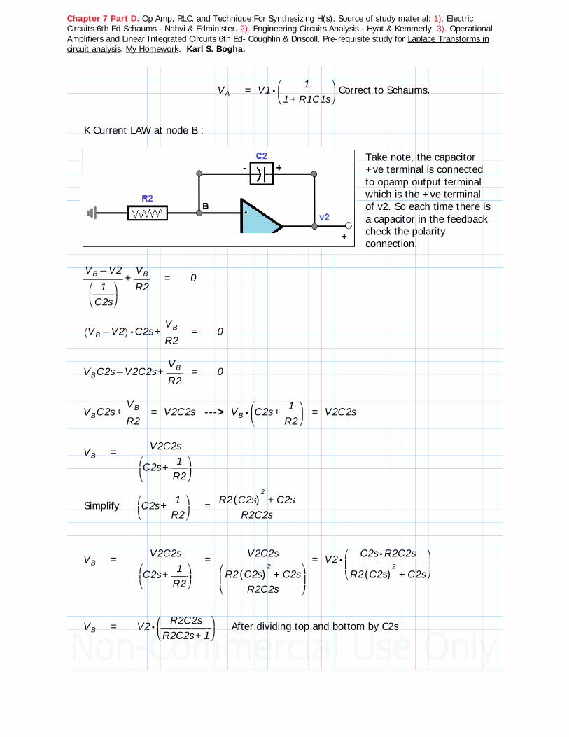
Chapter 7 Part D. Op Amp, RLC, and Technique For Synthesizing H(s). Source of study material: 1). Electric Circuits 6th Ed Schaums - Nahvi & Edminister. 2). Engineering Circuits Analysis - Hyat & Kemmerly. 3). Operational Amplifiers and Linear Integrated Circuits 6th Ed- Coughlin & Driscoll. Pre-requisite study for Laplace Transforms in circuit analysis. My Homework. Karl S. Bogha.
VA = ⋅V1 ⎛⎜⎝――――
1+1 R1C1s
⎞⎟⎠
Correct to Schaums.
K Current LAW at node B :
Take note, the capacitor +ve terminal is connected to opamp output terminal which is the +ve terminal of v2. So each time there is a capacitor in the feedback check the polarity connection.
+―――−VB V2
⎛⎜⎝――1C2s⎞⎟⎠
――VB
R2= 0
+⋅⎛⎝ −VB V2⎞⎠ C2s ――VB
R2= 0
+−VBC2s V2C2s ――VB
R2= 0
+VBC2s ――VB
R2= V2C2s ---> ⋅VB
⎛⎜⎝
+C2s ――1
R2⎞⎟⎠
= V2C2s
VB = ――――V2C2s
⎛⎜⎝
+C2s ――1R2⎞⎟⎠
Simplify ⎛⎜⎝
+C2s ――1
R2⎞⎟⎠
= ――――――+R2 ((C2s))2
C2sR2C2s
VB = ――――V2C2s
⎛⎜⎝
+C2s ――1R2⎞⎟⎠
= ――――――V2C2s⎛⎜⎝――――――+R2 ((C2s))
2C2s
R2C2s
⎞⎟⎠
= ⋅V2 ⎛⎜⎝――――――
⋅C2s R2C2s
+R2 ((C2s))2
C2s
⎞⎟⎠
VB = ⋅V2 ⎛⎜⎝――――
R2C2s+R2C2s 1⎞⎟⎠
After dividing top and bottom by C2s

Chapter 7 Part D. Op Amp, RLC, and Technique For Synthesizing H(s). Source of study material: 1). Electric Circuits 6th Ed Schaums - Nahvi & Edminister. 2). Engineering Circuits Analysis - Hyat & Kemmerly. 3). Operational Amplifiers and Linear Integrated Circuits 6th Ed- Coughlin & Driscoll. Pre-requisite study for Laplace Transforms in circuit analysis. My Homework. Karl S. Bogha.
VB = ⋅V2 ⎛⎜⎝――――
R2C2s+1 R2C2s
⎞⎟⎠
Correct to Schaums.
Set VA = VB, under ideal opamp conditions. Node A = 0, Node B= Node A = 0.
VA = VB
⋅V1 ⎛⎜⎝――――
1+1 R1C1s
⎞⎟⎠
= ⋅V2 ⎛⎜⎝――――
R2C2s+1 R2C2s
⎞⎟⎠
H ((s)) = ――V2V1
= ―――――
⎛⎜⎝――――1
+1 R1C1s⎞⎟⎠
⎛⎜⎝――――R2C2s
+1 R2C2s⎞⎟⎠
= ⋅⎛⎜⎝――――
1+1 R1C1s
⎞⎟⎠⎛⎜⎝――――
+1 R2C2sR2C2s
⎞⎟⎠
H ((s)) = ―――――――+1 R2C2s
(( +1 R1C1s)) ((R2C2s))Answer.
Now set R1C1 = R2C2 in H(s):
H ((s)) = ―――――――+1 R1C1s
(( +1 R1C1s)) ((R1C1s))= ―――――――
(( +1 R1C1s))(( +1 R1C1s)) ((R1C1s))
= ―――1
R1C1s
H ((s)) = ――V2V1
= ―――1
R1C1s
Circuit to the left is from section 2 Schaums 5.11 notes on Integrator and differentiator circuits.
v2 = −――1
RC⌠⌡ dv1 t
The transfer function here resulted in a +ve (1/RCs) which makes it a non-inverting integrator. V1 is connected to terminal A ie +ve.
v2 = ⋅v1 ―――1
R1C1sThe conclusion is correct its a non-inverting integrator circuit. s being the complex frequency.
v2 = ――1
RCs⌠⌡ dv1 t Answer. Shown in small caps for v representing
time domain, large cap for phasor.
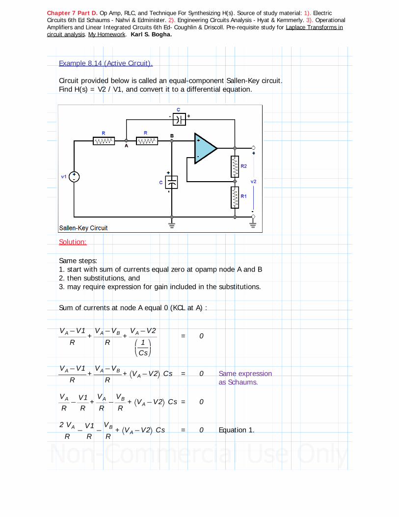
Chapter 7 Part D. Op Amp, RLC, and Technique For Synthesizing H(s). Source of study material: 1). Electric Circuits 6th Ed Schaums - Nahvi & Edminister. 2). Engineering Circuits Analysis - Hyat & Kemmerly. 3). Operational Amplifiers and Linear Integrated Circuits 6th Ed- Coughlin & Driscoll. Pre-requisite study for Laplace Transforms in circuit analysis. My Homework. Karl S. Bogha.
Example 8.14 (Active Circuit).
Circuit provided below is called an equal-component Sallen-Key circuit.Find H(s) = V2 / V1, and convert it to a differential equation.
Solution:
Same steps:1. start with sum of currents equal zero at opamp node A and B2. then substitutions, and 3. may require expression for gain included in the substitutions.
Sum of currents at node A equal 0 (KCL at A) :
++―――−VA V1R
―――−VA VB
R―――−VA V2⎛⎜⎝――1Cs⎞⎟⎠
= 0
++―――−VA V1R
―――−VA VB
R⎛⎝ −VA V2⎞⎠ Cs = 0 Same expression
as Schaums.
+−+−――VA
R――V1R
――VA
R――VB
R⎛⎝ −VA V2⎞⎠ Cs = 0
+−−――2 VA
R――V1R
――VB
R⎛⎝ −VA V2⎞⎠ Cs = 0 Equation 1.

Chapter 7 Part D. Op Amp, RLC, and Technique For Synthesizing H(s). Source of study material: 1). Electric Circuits 6th Ed Schaums - Nahvi & Edminister. 2). Engineering Circuits Analysis - Hyat & Kemmerly. 3). Operational Amplifiers and Linear Integrated Circuits 6th Ed- Coughlin & Driscoll. Pre-requisite study for Laplace Transforms in circuit analysis. My Homework. Karl S. Bogha.
Sum of currents at node B equal 0 (KCL at B):
+――VB
⎛⎜⎝――1Cs⎞⎟⎠
―――−VB VA
R= 0
+VBCs ―――−VB VA
R= 0 Same expression
as Schaums.
−+VBCs ――VB
R――VA
R= 0 Equation 2.
I place the 2 equations together to see what I got:
+−−――2 VA
R――V1R
――VB
R⎛⎝ −VA V2⎞⎠ Cs = 0 Equation 1.
−+VBCs ――VB
R――VA
R= 0 Equation 2.
Lets see if I can make a substitution, it does not look possible because vA is NOT connected to an opamp terminal, where I can set vA = vB = 0. So I shall try the gain expression to progress further.
The voltage at the positive terminal of the opamp is vB.
Let the gain be k some positive real number.
V2 = ⋅k VB
For my substitution I must have remaining in the expression V2.So that I may get V2/V1 eventually. Therefore I need to substitute vB for V2/k.
VB = ――V2k
Continued next page.

Chapter 7 Part D. Op Amp, RLC, and Technique For Synthesizing H(s). Source of study material: 1). Electric Circuits 6th Ed Schaums - Nahvi & Edminister. 2). Engineering Circuits Analysis - Hyat & Kemmerly. 3). Operational Amplifiers and Linear Integrated Circuits 6th Ed- Coughlin & Driscoll. Pre-requisite study for Laplace Transforms in circuit analysis. My Homework. Karl S. Bogha.
Since the -ve terminal is not connected to earth its voltage is not zero volts.However the difference between +ve and -ve terminals of the opamp is 0V.That is Ed = 0V = (+ve) - (-ve) terminal voltage.So now the voltage at the top of R1, shown as C, is vB volts.
VC = VB = ――V2k
I = ――VB
R1I is current flowing thru R1. It looks like R1 is a voltage source circuit wise providing current to R2.
V2 = ⋅I (( +R1 R2)) = ⋅⎛⎜⎝――VB
R1⎞⎟⎠
(( +R1 R2)) = ⋅VB⎛⎜⎝
+――R1R1
――R2R1⎞⎟⎠
V2 = ⋅VB⎛⎜⎝
+1 ――R2R1⎞⎟⎠
Since VB = ――V2k
V2 = ⋅――V2k⎛⎜⎝
+1 ――R2R1⎞⎟⎠
⋅V2 k = ⋅V2 ⎛⎜⎝+1 ――
R2R1⎞⎟⎠
Cancelling V2 both sides
k = +1 ――R2R1

Chapter 7 Part D. Op Amp, RLC, and Technique For Synthesizing H(s). Source of study material: 1). Electric Circuits 6th Ed Schaums - Nahvi & Edminister. 2). Engineering Circuits Analysis - Hyat & Kemmerly. 3). Operational Amplifiers and Linear Integrated Circuits 6th Ed- Coughlin & Driscoll. Pre-requisite study for Laplace Transforms in circuit analysis. My Homework. Karl S. Bogha.
k = +1 ――R2R1
Correct to Schaums.
Next I try to solve for V2/V1.
+−−――2 VA
R――V1R
――VB
R⎛⎝ −VA V2⎞⎠ Cs = 0 Equation 1.
−−−VA⎛⎜⎝
+―2R
Cs⎞⎟⎠VB⎛⎜⎝―1R⎞⎟⎠
V1 ⎛⎜⎝―1R⎞⎟⎠
V2 ((Cs)) = 0
I substitute vB for V2/K in equation 1 :
−−−VA⎛⎜⎝
+―2R
Cs⎞⎟⎠V2 ⎛⎜⎝
――1
kR⎞⎟⎠
V1 ⎛⎜⎝―1R⎞⎟⎠
V2 ((Cs)) = 0
−−VA⎛⎜⎝
+―2R
Cs⎞⎟⎠V1 ⎛⎜⎝
―1R⎞⎟⎠
V2 ⎛⎜⎝+――
1kR
Cs⎞⎟⎠= 0 Equation 3.
Looking at Equation 2 perform similar substitution to equation 1.
−+VBCs ――VB
R――VA
R= 0 Equation 2.
Equation 3 needs vA in terms of V1 and V2.
Substitute vB for V2/k in equation 2.
−+⎛⎜⎝――V2k⎞⎟⎠
Cs ――
⎛⎜⎝――V2
k⎞⎟⎠
R――VA
R= −+V2 ⎛⎜⎝
――Csk⎞⎟⎠
V2 ⎛⎜⎝――
1kR⎞⎟⎠
VA⎛⎜⎝―1R⎞⎟⎠
= 0
――VA
R= V2 ⎛⎜⎝
+――Csk
――1
kR⎞⎟⎠
VA = ⋅V2 R ⎛⎜⎝+――
Csk
――1
kR⎞⎟⎠
VA = V2 ⎛⎜⎝+――
RCsk
―1k⎞⎟⎠
Equation 4.
Substitute vA in equation 4 into equation 3.

Chapter 7 Part D. Op Amp, RLC, and Technique For Synthesizing H(s). Source of study material: 1). Electric Circuits 6th Ed Schaums - Nahvi & Edminister. 2). Engineering Circuits Analysis - Hyat & Kemmerly. 3). Operational Amplifiers and Linear Integrated Circuits 6th Ed- Coughlin & Driscoll. Pre-requisite study for Laplace Transforms in circuit analysis. My Homework. Karl S. Bogha.
−−V2 ⎛⎜⎝+――
RCsk
―1k⎞⎟⎠⎛⎜⎝
+―2R
Cs⎞⎟⎠V1 ⎛⎜⎝
―1R⎞⎟⎠
V2 ⎛⎜⎝+――
1kR
Cs⎞⎟⎠= 0
−V2 ⎛⎜⎝+――
RCsk
―1k⎞⎟⎠⎛⎜⎝
+―2R
Cs⎞⎟⎠V2 ⎛⎜⎝
+――1
kRCs⎞⎟⎠
= V1 ⎛⎜⎝―1R⎞⎟⎠
−V2⎛⎜⎝
+++⎛⎜⎝―――2 RCs
kR⎞⎟⎠
⎛⎜⎝―――RC2 s2
k
⎞⎟⎠⎛⎜⎝――
2kR⎞⎟⎠⎛⎜⎝――Csk⎞⎟⎠
⎞⎟⎠
V2 ⎛⎜⎝+――
1kR
Cs⎞⎟⎠= V1 ⎛⎜⎝
―1R⎞⎟⎠
V2⎛⎜⎝
−−+++⎛⎜⎝――2 CskR⎞⎟⎠
⎛⎜⎝―――RC2 s2
k
⎞⎟⎠⎛⎜⎝――
2kR⎞⎟⎠⎛⎜⎝――Csk⎞⎟⎠⎛⎜⎝――
1kR⎞⎟⎠
((Cs))⎞⎟⎠
= V1 ⎛⎜⎝―1R⎞⎟⎠
Multiply by k
V2 ⎛⎜⎝−−+++⎛
⎜⎝――2 Cs
R⎞⎟⎠⎛⎝RC2 s2 ⎞⎠ ⎛⎜⎝
―2R⎞⎟⎠
((Cs)) ⎛⎜⎝―1R⎞⎟⎠
((Csk))⎞⎟⎠= V1 ⎛⎜⎝
―kR⎞⎟⎠
――V2V1
= ―――――――――――――――
⎛⎜⎝―kR⎞⎟⎠
⎛⎜⎝
−−+++⎛⎜⎝――2 Cs
R⎞⎟⎠⎛⎝RC2 s2 ⎞⎠ ⎛⎜⎝
―2R⎞⎟⎠
((Cs)) ⎛⎜⎝―1R⎞⎟⎠
((Csk))⎞⎟⎠
――V2V1
= ―――――――――――――――
⎛⎜⎝―kR⎞⎟⎠
−+++⎛⎝RC2 s2 ⎞⎠ ⎛⎜⎝――2 Cs
R⎞⎟⎠
((Cs)) ⎛⎜⎝―1R⎞⎟⎠
(( −2 1)) ((Csk))Next multiply by R top and bottom.
――V2V1
= ―――――――――――――――((k))
−+++⎛⎝R2 C2 s2 ⎞⎠ ((2 Cs)) ((RCs)) (( −2 1)) ((RCsk))
――V2V1
= ――――――――――――――((k))
−+++⎛⎝R2 C2 s2 ⎞⎠ ((2 Cs)) ((RCs)) ((1)) ((RCsk))Continuing with my simplification.
――V2V1
= ―――――――――――((k))
++⎛⎝R2 C2 s2 ⎞⎠ ⋅⎛⎜⎝
−+―2R
1 k⎞⎟⎠RCs 1
My expression thus far.
Schaums solution has the 2nd term (3-k) I have ((2/R)+1-k)2/R is reduced to 2 because 1/R is very small that it can be ignored leaving 2. Completely ignore 1/R as in removing it.
――V2V1
= ――――――――――((k))
++R2 C2 s2 (( −+2 1 k)) RCs 1
――V2V1
= ―――――――――((k))
++R2 C2 s2 (( −3 k)) RCs 1R is large. (1/R) is much lower resistance, implies closer to conductance. Leaving it our does not impact the circuit, because its no longer impedance/resistance. Leave (1/R) and hold 2.

Chapter 7 Part D. Op Amp, RLC, and Technique For Synthesizing H(s). Source of study material: 1). Electric Circuits 6th Ed Schaums - Nahvi & Edminister. 2). Engineering Circuits Analysis - Hyat & Kemmerly. 3). Operational Amplifiers and Linear Integrated Circuits 6th Ed- Coughlin & Driscoll. Pre-requisite study for Laplace Transforms in circuit analysis. My Homework. Karl S. Bogha.
――V2V1
= ―――――――――((k))
++⎛⎝R2 C2 s2 ⎞⎠ (( −3 k)) RCs 1Answer. <--- Schaums has this
expression. Reader verify.
I suggest you-reader-student-engineer check with local lecturer or engineer.
Continuing with my expression:
――V2V1
= ―――――――――((k))
++R2 C2 s2 (( −3 k)) RCs 1
V2 ⎛⎝ ++R2 C2 s2 (( −3 k)) RCs 1⎞⎠ = kV1
++R2 C2 s2 V2 (( −3 k)) RCsV2 V2 = kV1
Next convert to differential equation:
s2 : ――d2 v2
dt2
s : ――dv2dt
++R2 C2 ⎛⎜⎝――d2 v2
dt2
⎞⎟⎠
(( −3 k)) RC ⎛⎜⎝――dv2dt⎞⎟⎠
v2 = kv1 Answer.
Comments:
(2/R) + 1 - k :
Regarding (2/R) is the same as 2 x (1/R).My solution has the condition (1/R) is small its impact is negligible because R is large. If R is 2000 then 1/R equals 0.001. That would make the coefficient (numerator) 2 reduced from 2 to 0.002. (1/R) not made zero rather removed. Leaving the 2 from (2/R). Resistance was so large, its inverse is supporting admittance or conductance.
If you can find the same solution thru another process or steps great.Otherwise continue with the present solution I have.

Chapter 7 Part D. Op Amp, RLC, and Technique For Synthesizing H(s). Source of study material: 1). Electric Circuits 6th Ed Schaums - Nahvi & Edminister. 2). Engineering Circuits Analysis - Hyat & Kemmerly. 3). Operational Amplifiers and Linear Integrated Circuits 6th Ed- Coughlin & Driscoll. Pre-requisite study for Laplace Transforms in circuit analysis. My Homework. Karl S. Bogha.
Example 8.15 (Active Circuit).
In the circuit below, assume R = 2kohm, c =10nF, and R2 = R1.Find v2 if v1 = u(t).
Quote: 'One tangential error can drive a man into eternity trying to solve a problem, so consider giving up time wise and let the other party have the victory' -Karl Bogha.
Talking about long attempts on solutions. This may apply in business and engineering.
My solution is long but its easy to follow.
Solution:v1 equal a unit step function. This means v1 comes on at time t=0 and its a unit value. Unit value can be assumed to 1 in this case. I know the unit step value can be 10, with a multiplier of 10, and remains a constant 10 for t>0. Just so its the same value. Usually its ON and equal 1 at t>0.Plug in the electrical component values in H(s) found in example 8.14:
≔R 2000 ≔C ⋅10 10−9 <---10 Nano Farad
H ((s)) = ――V2V1
= ―――――――――((k))
++⎛⎝R2 C2 s2 ⎞⎠ (( −3 k)) RCs 1Using Schaums expression from Example 8.14.
=⋅R2 C2 ⋅400 10−12 =⋅R C ⋅20 10−6 =⋅⋅2 R C ⋅4 10−5
k = +1 ――R2R1
k = =+1 ―11
2 Since R1=R2 their division results in 1.
――V2V1
= ―――――――――((k))
++⎛⎝R2 C2 s2 ⎞⎠ (( −3 2)) RCs 1= ―――――――
((k))
++⎛⎝R2 C2 s2 ⎞⎠ RCs 1
H ((s)) = ――V2V1
= ――――――――2
++⋅4 10−10 s2 ⋅2 10−5 s 1Answer.Same as Schaums.

Chapter 7 Part D. Op Amp, RLC, and Technique For Synthesizing H(s). Source of study material: 1). Electric Circuits 6th Ed Schaums - Nahvi & Edminister. 2). Engineering Circuits Analysis - Hyat & Kemmerly. 3). Operational Amplifiers and Linear Integrated Circuits 6th Ed- Coughlin & Driscoll. Pre-requisite study for Laplace Transforms in circuit analysis. My Homework. Karl S. Bogha.
Using the transfer function H(s), I can sove for v2, since v1 is a step function for t>0.
―v2v1
= ――――――――2
++⋅4 10−10 s2 ⋅2 10−5 s 1
v2 = ――――――――⋅((v1)) 2
++⋅4 10−10 s2 ⋅2 10−5 s 1v1 = u(t) = 1 for t>0
v2 = ――――――――2
++⋅4 10−10 s2 ⋅2 10−5 s 1t > 0
For the differential equation:
++R2 C2 ⎛⎜⎝――d2 v2
dt2
⎞⎟⎠
(( −3 k)) RC ⎛⎜⎝――dv2dt⎞⎟⎠
v2 = kv1 Differential equation.
=⋅R2 C2 ⋅400 10−12 ≔k 2 =⋅⋅(( −3 k)) R C ⋅20 10−6 =⋅R C ⋅20 10−6
Plug into differential equation:
++⋅4 10−10 ⎛⎜⎝――d2 v2
dt2
⎞⎟⎠
⋅2 10−5 ⎛⎜⎝――dv2dt⎞⎟⎠
v2 = ⋅2 v1
Divide by 4 x 10^-10, and the new coefficients :
=―――⋅4 10−10
⋅4 10−101 =―――
⋅2 10−5
⋅4 10−10⋅50 103 =―――
1
⋅4 10−10⋅2.5 109 =―――
2
⋅4 10−10⋅5 109
Use: ⋅5 104 Use: ⋅25 108
++1⎛⎜⎝――d2 v2
dt2
⎞⎟⎠
⋅5 104 ⎛⎜⎝――dv2dt⎞⎟⎠
⋅25 108 v2 = ⋅⋅5 109 v1
++⎛⎜⎝――d2 v2
dt2
⎞⎟⎠
⋅5 104 ⎛⎜⎝――dv2dt⎞⎟⎠
⋅25 108 v2 = ⋅⋅5 109 v1 <--- This is what I got same as Schaums. Answer.
Continued next page.

Chapter 7 Part D. Op Amp, RLC, and Technique For Synthesizing H(s). Source of study material: 1). Electric Circuits 6th Ed Schaums - Nahvi & Edminister. 2). Engineering Circuits Analysis - Hyat & Kemmerly. 3). Operational Amplifiers and Linear Integrated Circuits 6th Ed- Coughlin & Driscoll. Pre-requisite study for Laplace Transforms in circuit analysis. My Homework. Karl S. Bogha.
Continuing with the solution for v2.The response to v1 = u(t) = 1 for t>0.
++⎛⎜⎝――d2 v2
dt2
⎞⎟⎠
⋅5 104 ⎛⎜⎝――dv2dt⎞⎟⎠
⋅25 108 v2 = ⋅⋅5 109 u ((t)) = ⋅⋅5 109 1 = ⋅5 109
−+⋅⋅5 104 s2 ⋅⋅25 108 s ⋅5 109 = 0 <--- The roots here may provide the path to the solution.
Divide by 10^4 :
−+5 s2 ⋅⋅25 104 s ⋅5 105 = 0
Divide by 5 : −+s2 ⋅⋅5 104 s ⋅1 105 = 0 <--- Quadratic equation.
++Ax2 Bx C = 0
≔A 1 ≔B ⋅5 104 ≔C ⋅−1 105
Solve the quadratic equation for the roots of s :
≔SqrtTerm =‾‾‾‾‾‾‾‾‾‾‾‾‾−⎛⎝B2 ⎞⎠ (( ⋅⋅4 A C)) 50004
sp1 = =―――――+−B SqrtTerm⋅2 A
1.9999 = 2.0 <--- Real root > 0.
sp2 = =―――――−−B SqrtTerm⋅2 A
−50001.9999 = −50000 <--- Imaginary root < 0.
Next I try to form an equation for the dc/steady state and natural/transient condition.
My problem(s): 1) - I do not know if its over, under, or critically damped circuit? Because I have two roots, in my thinking it should be an over damped case. But the solution makes no note of that instead starts for an underdamped case. 2) - I do not have L in the circuit to apply the typical formulas for determing the damped case. Obviously I cannot use the 1/(Sqrt LC).3) - Right-off I am unable to form an equation, though I have the two roots.
s1 = +−――1
2 RC
‾‾‾‾‾‾‾‾‾‾‾‾‾−⎛
⎜⎝――
12 RC
⎞⎟⎠
2 ⎛⎜⎝――
1LC⎞⎟⎠
= +−α ‾‾‾‾‾‾‾−α2 ω02 <---For a parallel RLC circuit
the 2 expressions are available in textbook and Schaums. However I do not have L in this circuit. Check textbook for full details.
= +−α β
s1 = −−――1
2 RC
‾‾‾‾‾‾‾‾‾‾‾‾‾−⎛
⎜⎝――
12 RC
⎞⎟⎠
2 ⎛⎜⎝――
1LC⎞⎟⎠
= −−α ‾‾‾‾‾‾‾−α2 ω02
= −−α β

Chapter 7 Part D. Op Amp, RLC, and Technique For Synthesizing H(s). Source of study material: 1). Electric Circuits 6th Ed Schaums - Nahvi & Edminister. 2). Engineering Circuits Analysis - Hyat & Kemmerly. 3). Operational Amplifiers and Linear Integrated Circuits 6th Ed- Coughlin & Driscoll. Pre-requisite study for Laplace Transforms in circuit analysis. My Homework. Karl S. Bogha.
s1 = +−――R
2 L
‾‾‾‾‾‾‾‾‾‾‾‾−⎛
⎜⎝――
R2 L⎞⎟⎠
2 ⎛⎜⎝――
1LC⎞⎟⎠
= +−α β <---For a series RLC circuitthe 2 expressions are available in textbook and Schaums. Again I do not have L in this circuit. Check textbook for full details.s1 = −−――
R2 L
‾‾‾‾‾‾‾‾‾‾‾‾−⎛
⎜⎝――
R2 L⎞⎟⎠
2 ⎛⎜⎝――
1LC⎞⎟⎠
= −−α β
I can say its an RC circuit since there is no L in it. Thru my sketch on the next page I identify it a parallel RC circuit. Not merely because I am trying to fix it to the Schaum's solution but I can isolate the Rf and Ri in the circuit.
Isolate R and C as shown in the figure. R for Ri, and C for Rf.
Parallel RC: α = ―――1⋅⋅2 R C
ω0 = ――1
‾‾‾LC
Proceed with alpha: ≔R 2000 ≔C ⋅10 10−9
α = =―――1⋅⋅2 R C
25000 Schaums shows 25,000 for alpha, but not how they got it ? If not the same method. You check.
I may go around the w0 situation thru equating the root(s).I equate the roots to complex frequency s with sigma = 0.
≔j ‾‾‾−1 The complex frequencies:
s1 = +σ jω = +0 j2 = ω1 = 2
s2 = +σ jω = −0 j50000 = ω2 = −50000

Chapter 7 Part D. Op Amp, RLC, and Technique For Synthesizing H(s). Source of study material: 1). Electric Circuits 6th Ed Schaums - Nahvi & Edminister. 2). Engineering Circuits Analysis - Hyat & Kemmerly. 3). Operational Amplifiers and Linear Integrated Circuits 6th Ed- Coughlin & Driscoll. Pre-requisite study for Laplace Transforms in circuit analysis. My Homework. Karl S. Bogha.
Right now I have ONE alpa value and TWO omega values 2 and -50,000.Which of the two omega values apply? First whats their period T equal.
ω0 = 2 πf T = ―1f
= ――2 πω0
= ――2 πω0
T1 = =――2 π
23.1416 T2 = =―――
2 π||−50000||
⋅125.66 10−6 = ⋅0.1256 10−3
Practically 0.
T2 = =―――2 π
||−75000||⋅83.78 10−6 = ⋅0.083 10−3 Practically 0. -75000 Comes up later.
However, RLC circuits do operate in the millisecond range.
Next I compare alpha to omega(s):
α2 = =250002 ⋅625 106 Greater Than > ω12 = 4 Over damped
α2 = =250002 ⋅625 106 Less Than < ω22 = ⋅2.5 109 Under damped
Can the circuit have both conditions Over and Under damped? I try to work both to meet the answer. Would be my first? I may had this problem in one example in previous parts. It may been the lengthy discussion.
Underdamped case alpha is less than w.
v ((t)) = e−αt (( +A1cos ((β t)) A2sin ((β t)))) <--- Under damped equation. Both Beta are the same.
s = +α jβ
s2 = −50000 = +α jβ = +25000 jβ1 ; +' jβ = =−−50000 25000 −75000
s2 = −50000 = −α jβ = −25000 jβ2 ; −jβ = =−−50000 25000 −75000
+α jβ1 = −25000 j75000 Both Beta 1 and Beta 2 are the same. I know from the Notes, Beta is the angular frequency w for under damped case. Both same not beta 1 and Beta 2, rather just Beta.
−α jβ2 = −25000 j75000
v2 ((t)) = e−αt (( +A1cos ((β t)) A2sin ((β t))))
v2 ((t)) = e−25000 t (( +A1cos ((−75000 t)) A2sin ((−75000 t)))) Equation 1
Continued next page.

Chapter 7 Part D. Op Amp, RLC, and Technique For Synthesizing H(s). Source of study material: 1). Electric Circuits 6th Ed Schaums - Nahvi & Edminister. 2). Engineering Circuits Analysis - Hyat & Kemmerly. 3). Operational Amplifiers and Linear Integrated Circuits 6th Ed- Coughlin & Driscoll. Pre-requisite study for Laplace Transforms in circuit analysis. My Homework. Karl S. Bogha.
Over damped case alpha is greater than w.
v2 ((t)) = +A1e ⋅s1 t A2e ⋅s2 t <--- Over damped equation.
s1 = 2 and s2 = −50000
v2 ((t)) = +A1e2 t A2e−50000 t Equation 2
At time t>0 when the capacitor is fully charged.The voltage v2 equal the capacitor voltage vC.
vC = ⎛⎜⎝―1C⎞⎟⎠⌠⌡ d0
t
i t
――dvC
dt= ⎛
⎜⎝―1C⎞⎟⎠
(( −i ((t)) i ((0)))) = ⎛⎜⎝―1C⎞⎟⎠
(( −i ((t)) 0)) = ⎛⎜⎝―1C⎞⎟⎠
i ((t))
++⎛⎜⎝――d2 v2
dt2
⎞⎟⎠
⋅5 104 ⎛⎜⎝――dv2dt⎞⎟⎠
⋅25 108 v2 = ⋅⋅5 109 u ((t)) = ⋅⋅5 109 1 = ⋅5 109
Divide by the coefficient of v1, to make it unity on LHS because its u(t).
++⋅―――1
⋅5 109
⎛⎜⎝――d2 v2
dt2
⎞⎟⎠
⋅―――⋅5 104
⋅5 109
⎛⎜⎝――dv2dt⎞⎟⎠
⋅―――⋅25 108
⋅5 109v2 = ⋅―――
⋅5 109
⋅5 109u ((t))
=―――1
⋅5 109⋅200 10−12 Approximatley equal zero.
++⋅0⎛⎜⎝――d2 v2
dt2
⎞⎟⎠
⋅⋅1 10−5 ⎛⎜⎝――dv2dt⎞⎟⎠
⋅0.5 v2 = ⋅1 u ((t))
⋅⋅1 10−5 ⎛⎜⎝――dv2dt⎞⎟⎠
= +⋅−0.5 v2 ⋅1 u ((t)) u(t) can be removed.
⎛⎜⎝――dv2dt⎞⎟⎠
= 100000 (( +⋅−0.5 v2 1)) Inverse of 1 x 10^-5: =―――1
⋅1 10−5100000
⎛⎜⎝――dv2dt⎞⎟⎠
= +⋅−50000 v2 100000
――dvC
dt= ⎛
⎜⎝――dv2dt⎞⎟⎠
= +⋅−50000 v2 100000 Substitute into the dvC/dt equation.

Chapter 7 Part D. Op Amp, RLC, and Technique For Synthesizing H(s). Source of study material: 1). Electric Circuits 6th Ed Schaums - Nahvi & Edminister. 2). Engineering Circuits Analysis - Hyat & Kemmerly. 3). Operational Amplifiers and Linear Integrated Circuits 6th Ed- Coughlin & Driscoll. Pre-requisite study for Laplace Transforms in circuit analysis. My Homework. Karl S. Bogha.
⎛⎜⎝――dv2dt⎞⎟⎠
= ――dvC
dt= ⎛
⎜⎝―1C⎞⎟⎠
i ((t)) = +⋅−50000 v2 100000
At time t = 0, the vC = 0, dvC/dt at a short interval close to t=0 results in capacitor voltage equal zero, dividied by time dt results in 0. dvc/dt at t = 0 equal zero. OR lets say vC at t=0 is some constant in this case u(t) its derivative will be? Zero. So in both cases I have dvC/dt = 0 = dv2/dt.
⎛⎜⎝――dv2dt⎞⎟⎠
= +−0.0005 v2 0.001
0 = +−0.0005 v2 0.001
0.0005 v2 = 0.001
v2 = =―――0.001
0.00052 V. At time t=0.
v2 = 2 V. Answer. <--- This can be called the dc voltage or the forced response. It has to be since its a constant value. I did not expect to get this result thru my process. Its part of the solution for the forced response or steady state.
Same answer as Schaums.
Note: Schaums did not show how this answer, the dc part, was arrived at. Just that in the final answer its 2V.
First derivative of equation 1 (Under damped case) :
v2 ((t)) = e−25000 t (( +A1cos ((−75000 t)) A2sin ((−75000 t)))) Equation 1
v2 ((t)) = +⋅e−25000 t A1cos ((−75000 t)) ⋅e−25000 t A2sin ((−75000 t))
Trignometry property that can be applied here, because I see the negative sign. sin ((t)) = −sin ((−t))
cos ((t)) = cos ((−t))
Differentiation of sin and cos : ――――d ((sin ((t))))
dt= cos ((t)) ――――
d ((cos ((t))))dt
= −sin ((t))
Differentiaion of two --->terms in the expression above for v2(t):
――――――d ((sin ((−75000 t))))
dt= ⋅−75000 cos ((75000 t))
――――――d ((cos ((−75000 t))))
dt= ⋅−75000 sin ((75000 t))

Chapter 7 Part D. Op Amp, RLC, and Technique For Synthesizing H(s). Source of study material: 1). Electric Circuits 6th Ed Schaums - Nahvi & Edminister. 2). Engineering Circuits Analysis - Hyat & Kemmerly. 3). Operational Amplifiers and Linear Integrated Circuits 6th Ed- Coughlin & Driscoll. Pre-requisite study for Laplace Transforms in circuit analysis. My Homework. Karl S. Bogha.
v2 ((t)) = +⋅e−25000 t A1cos ((−75000 t)) ⋅e−25000 t A2sin ((−75000 t))
――dv2dt
= ⎛⎝ +⋅−25000 e−25000 t A1cos ((−75000 t)) ((−75000)) e−25000 t A1sin ((75000 t))⎞⎠
+' ⎛⎝ +⋅−25000 e−25000 t A2sin ((−75000 t)) ((−75000)) e−25000 t A2cos ((75000 t))⎞⎠
――dv2dt
= −⋅−25000 e−25000 t A1cos ((75000 t)) 75000 e−25000 t A1sin ((75000 t))
−+' ⋅25000 e−25000 t A2sin ((75000 t)) 75000 e−25000 t A2cos ((75000 t))
Since vC = v2 and ――dvC
dt= ――
dv2dt
vC = 2 Then ――dvC
dt= ――
d ((2))dt
= 0
0 = −⋅−25000 e−25000 t A1cos ((75000 t)) 75000 e−25000 t A1sin ((75000 t))
−+' ⋅25000 e−25000 t A2sin ((75000 t)) 75000 e−25000 t A2cos ((75000 t))Equation 3
Placing equation 1 here for reference :
v2 ((t)) = e−25000 t (( +A1cos ((−75000 t)) A2sin ((−75000 t)))) Equation 1
Let t = 0 for Equation 1, then v2(0) = 2V :
2 = +1 A1cos ((0)) A2sin ((0))2 = +A1 ⋅A2 02 = A1 Equation 4
Let t = 0 for Equation 3 :
0 = −⋅⋅−25000 1 A1cos ((0)) ⋅75000 1 A1sin ((0))−+' ⋅⋅25000 1 A2sin ((0)) ⋅⋅75000 1 A2cos ((0))
0 = −−25000 A1 75000 A2 Equation 5
Substitute A1 = 2
0 = −⋅−25000 2 75000 A2 = −−50000 75000 A2
75000 A2 = −50000

Chapter 7 Part D. Op Amp, RLC, and Technique For Synthesizing H(s). Source of study material: 1). Electric Circuits 6th Ed Schaums - Nahvi & Edminister. 2). Engineering Circuits Analysis - Hyat & Kemmerly. 3). Operational Amplifiers and Linear Integrated Circuits 6th Ed- Coughlin & Driscoll. Pre-requisite study for Laplace Transforms in circuit analysis. My Homework. Karl S. Bogha.
A2 = =―――−5000075000
−0.6667
Substitute A1 and A2 in equation below:
v2 ((t)) = e−25000 t (( +A1cos ((−75000 t)) A2sin ((−75000 t))))
v2 ((t)) = −e−25000 t 2 cos ((75000 t)) 0.667 sin ((−75000 t))
sin ((7500)) = −sin ((−7500 t))v2 ((t)) = +e−α t 2 cos ((ω t)) 0.667 sin ((ω t))
=‾‾‾‾‾‾‾‾‾‾‾‾‾+22 ((−0.6667))2 2.1082 =atan⎛⎜⎝−―――
0.66672⎞⎟⎠−18.4358 deg
=−180 deg 18.4358 deg 161.5642 deg-18.43 degs is in the 4th quadrant, to make it positive in the clockwise direction subtract it from 180 degs.
With the cosine expression, we have the real term, without the imaginary sin term which is associated to j.
v2 ((t)) = ⋅2.108 e−α t cos (( +ω t 161.56 deg))
a = 25000 ω = 75000
Complete response steady state (dc) and transient :
v2 ((t)) = +2 ⋅2.108 e−α t cos (( +ω t 161.56 deg)) My Answer. My Attempt:I call it my attempt because I did not get the same answer to Schaums.
Schaums has a different answer. Provided below.
Schaums' solution / answer provided below.
The response of the preceeding equation for t>0 to v1 = u(t) is
v2 = +2 e−αt (( −2 cosωt 2.31 sinωt))
= +2 3.055 e−αt cos (( +ωt 130.9 °)) Schaums Answer.
where α = 25000ω = 21651 Rad/s Schaums Answer.
Comments: My solution's answer is not the same for the underdamped equation for v2. I have an error somewhere, and may have used the wrong approch. I suggest you check with your local lecturer and or engineer.

Chapter 7 Part D. Op Amp, RLC, and Technique For Synthesizing H(s). Source of study material: 1). Electric Circuits 6th Ed Schaums - Nahvi & Edminister. 2). Engineering Circuits Analysis - Hyat & Kemmerly. 3). Operational Amplifiers and Linear Integrated Circuits 6th Ed- Coughlin & Driscoll. Pre-requisite study for Laplace Transforms in circuit analysis. My Homework. Karl S. Bogha.
Plot of My solution and Schaums solution:
Periot T based on My w : =―――⋅2 π
750000.0000838
Schaums (SCH) Period T based w : =―――2 π
216510.0002902
≔v2 ((t)) +2 ⋅2.108 e−25000 t cos (( +⋅75000 t 161.56 deg))
≔v2_sch ((t)) +2 ⋅3.055 e−25000 t cos (( +⋅21651 t 130.9 deg))
0.4
0.6
0.8
1
1.2
1.4
1.6
1.8
2
2.2
2.4
2.6
2.8
0
0.2
3
0 0.00010.00010.00010.00010.00010.00020.00020.00020.00020.00020.00030.00030 0 0.0003
t
t
v2 ((t))
v2_sch ((t))
Comments:
My solution shows the under damped curve, and then settling at v2 equal 2 V.That matches the theory, the constant dc value continues with the transient dying out. Schaum's plot shown dashed is over damped, and settling at v2 equal 2V. Schaums plot does also look critically damped too but thats not possible unless alpha = omega. Which Schaums alpha = 25000 and omega = 21651 rad/s.

Chapter 7 Part D. Op Amp, RLC, and Technique For Synthesizing H(s). Source of study material: 1). Electric Circuits 6th Ed Schaums - Nahvi & Edminister. 2). Engineering Circuits Analysis - Hyat & Kemmerly. 3). Operational Amplifiers and Linear Integrated Circuits 6th Ed- Coughlin & Driscoll. Pre-requisite study for Laplace Transforms in circuit analysis. My Homework. Karl S. Bogha.
I have another attempt with the capacitors open circuit for time t>>0 next. Give it a short try. NOT impressive to me. If its not returning the results I give the engineers the victory on this problem!Capacitors shown open circuit. With my idea of current flow shown with arrows.
I show current flowing from the opamp -ve terminal to the top connection of resistor R1. This may not be there since the opamp's internal resistance is high. At most a very small current. I showed it more so to close the circuit's loop.
This figure its not cluttered looking.
Easier to follow.
The shaded areas are what I identify as two possible loops creating maybe a mesh analysis.
Lets say I know v1 equal u(t) so I set it equal to unity = 1.
iin = ――v1⋅2 R
= =―――1⋅2 2000
0.00025 = ⋅0.25 10−3 = 25 mA
Internal resistance of opamp is high. Therefore no appreciable current flow thru the opamp +ve terminal. Hence the voltage at -ve terminal is the same as +ve.v(+) = vB.v(-) = v(+) = vB = 0.
vB = 0In this circuit I do not see a voltage vB at top of resistor R1 thru connection to -ve terminal of opamp because the current is so low.

Chapter 7 Part D. Op Amp, RLC, and Technique For Synthesizing H(s). Source of study material: 1). Electric Circuits 6th Ed Schaums - Nahvi & Edminister. 2). Engineering Circuits Analysis - Hyat & Kemmerly. 3). Operational Amplifiers and Linear Integrated Circuits 6th Ed- Coughlin & Driscoll. Pre-requisite study for Laplace Transforms in circuit analysis. My Homework. Karl S. Bogha.
Grey shaded area sum of voltages KVL :Current thru Ris the same thru R2, its generated by the presence of voltage vB.v1 = ++vR vR vR1
v1 = −⋅⋅2 iin R ⋅iout R1 -ve sign for vR1 because current is i_out is opposite direction.
v1 = −⋅⋅⋅2 0.25 10−3 2000 ⋅iout R1 I will not set v1 = 1 here because it maybe used in another expression.v1 = −1 ⋅iout R1
Pink shaded area sum of voltages KVL :v2 = +vR1 vR2 Since R1 = R2 I make them both R1.v2 = 2 vR1v2 = ⋅⋅2 iout R1 Ok thats KVL but what have I gotten so far ?
So far nothing solution wise, continue with equations.
Can I equate something from v1 and v2?v1 = −1 ⋅iout R1 Equation 1v2 = ⋅⋅2 iout R1 Equation 2
From equation 1: iout = ⎛⎜⎝――−1 v1R1
⎞⎟⎠
From equation 2: iout = ――v22 R1
Substitute i_out above into equation 1.
v1 = −1 ⋅iout R1 = −1 ⋅⎛⎜⎝――
v22 R1
⎞⎟⎠
R1 = −1 ⎛⎜⎝―v22⎞⎟⎠
2 (( −v1 1)) = v2 I cannot form a transfer function of v2/v1, same when Isubstituted i_out from equation 1 into used equation 2
Comments: I may have done something wrong in my prior calculation. On these grey and pink shaded areas sum of voltages is not leading to the solution I seek. Which the solution has to be a exponential and sinusoidal expression. This path was not going to reveal much far as I know. Worst case error in Schaums solution. Would Laplace Transform help in this solution? Possible. It solves differential equations. However, these circuits problems are not meant to be solved using that technque here that comes in a later chapter.
Comments: Example 8.14, 15, and 16 are on the same circuit. I did not solve 15 completely got up to the differential equation and maybe the steady state of 2V (if my method was correct).
Missed the transient response. I solved example 8.16 coming next. Some consolation I have got a few and missed partially in 15. You are welcome to solve my errors.

Chapter 7 Part D. Op Amp, RLC, and Technique For Synthesizing H(s). Source of study material: 1). Electric Circuits 6th Ed Schaums - Nahvi & Edminister. 2). Engineering Circuits Analysis - Hyat & Kemmerly. 3). Operational Amplifiers and Linear Integrated Circuits 6th Ed- Coughlin & Driscoll. Pre-requisite study for Laplace Transforms in circuit analysis. My Homework. Karl S. Bogha.
Example 8.16 (Active Circuits):
Find conditions in the circuit below, same as Example 8.14, for sustained oscillations in v2(t) (with zero input) and find the frequency of oscillations.
Solution:
Transfer function got in example 8.14:
H ((s)) = ――V2V1
= ―――――――――((k))
++⎛⎝R2 C2 s2 ⎞⎠ (( −3 k)) RCs 1
The circuit must be in a sustained oscillation when there is no input voltage, that would be the transient response or natural response.
Engineers: For this to happen the roots, s1 s2, should be imaginary numbers in the characteristic equation.
Characteristic equation: ++⎛⎝R2 C2 s2 ⎞⎠ (( −3 k)) RCs 1Math refresher:
++Ax2 Bx C = 0 x1 = ―――――――+−B ‾‾‾‾‾‾‾‾‾‾−B2 ⋅⋅4 A C
⋅2 Ax2 = ―――――――
−−B ‾‾‾‾‾‾‾‾‾‾−B2 ⋅⋅4 A C⋅2 A
Roots real and UNequal −B2 ⋅⋅4 A C >' ' 0Roots real and Equal −B2 ⋅⋅4 A C = 0Roots Imaginary −B2 ⋅⋅4 A C <' ' 0 <--- Looking for this.

Chapter 7 Part D. Op Amp, RLC, and Technique For Synthesizing H(s). Source of study material: 1). Electric Circuits 6th Ed Schaums - Nahvi & Edminister. 2). Engineering Circuits Analysis - Hyat & Kemmerly. 3). Operational Amplifiers and Linear Integrated Circuits 6th Ed- Coughlin & Driscoll. Pre-requisite study for Laplace Transforms in circuit analysis. My Homework. Karl S. Bogha.
++⎛⎝R2 C2 s2 ⎞⎠ (( −3 k)) RCs 1
A = R2 C2
B = (( −3 k)) RC Reduce B so that its smaller than 4AC.C = 1
Since in this circuit problem we have (3-k) the value of k could be made 3, resulting in the parenthesis term to 0.
B = (( −3 3)) RC = 0
Now I have −02 ⋅⋅4 A C <' ' 0 a negative term.This results in a negative squareroot term - imaginary number.
x1 = ――――+−B jTerm⋅2 A
x2 = ――――−−B jTerm⋅2 A
Characteristic equation: ++⎛⎝R2 C2 s2 ⎞⎠ (( −3 3)) RCs 1
+⎛⎝R2 C2 s2 ⎞⎠ 1 = 0 For example making the expression zero, requires taking the v1 to the left, v2/v1..... , I ignore it here. R2 C2 s2 = −1
s2 = −―――1
R2 C2
sp1 , sp2 =‾‾‾‾‾‾‾−―――
1
R2 C2Imaginary numbers.
The roots would be the same numerical value but imaginary.This would make it oscillate between the two roots.
Example: =‾‾‾‾−16 4jSo it could be anywhere on the jw axis, positive or negative side. See figure --->
Schaum full answer: For sustained oscillations the roots of the characteristic equation in example 8.14 should be imaginary numbers. This happens when k=3 or R2 = 2R1, in which case w = 1/RC.
Next page for the R2=2R1.

Chapter 7 Part D. Op Amp, RLC, and Technique For Synthesizing H(s). Source of study material: 1). Electric Circuits 6th Ed Schaums - Nahvi & Edminister. 2). Engineering Circuits Analysis - Hyat & Kemmerly. 3). Operational Amplifiers and Linear Integrated Circuits 6th Ed- Coughlin & Driscoll. Pre-requisite study for Laplace Transforms in circuit analysis. My Homework. Karl S. Bogha.
We solved for k earlier in example 8.14.
k = +1 ――R2R1
R2 = 2 R1
k = +1 ――2 R1
R1Since R1=R2 their division results in 1.
k = +1 2 = 3
k = 3
The k criteria is satisfied when? R2 = 2R1. Thats the explanation at end of Schaums solution previous page.
This brings me to the end of the notes part on Schaums Chapter 8 'Higher Order Circuits and Complex Frequency'.
Next like Part 3C solving of a few Schaums Solved Problems and Supplementary Problems.
This is the last section to Part 3 to the prerequisite studies and skills for Laplace Transforms In Circuit Analysis. This brings me to that end.
Reader, student engineer and interested party, can start study on Differential Equations chapter on Lapalce Transforms and then get started to Schaums Chapter 16 in the 6th edition titled The Laplace Transform Method. You may use other editions or other textbooks.
Continued next page with the relevant problems.

Chapter 7 Part D. Op Amp, RLC, and Technique For Synthesizing H(s). Source of study material: 1). Electric Circuits 6th Ed Schaums - Nahvi & Edminister. 2). Engineering Circuits Analysis - Hyat & Kemmerly. 3). Operational Amplifiers and Linear Integrated Circuits 6th Ed- Coughlin & Driscoll. Pre-requisite study for Laplace Transforms in circuit analysis. My Homework. Karl S. Bogha.
Problem 8.19 (Magnitude scaling):
A 5000 rad/s sinusoidal source, V = 100@0deg V in phasor form,is applied to the circuit shown below.
Obtain the magnitude scaling factor Km and the element values which will limit the current to 89 mA (maximum value).
Solution:
Start with obtaining Zin: R and C are in series. They are in parallel to L2.Then that is in series to L1.
Zin = +jωL1 ――――――――⋅((jωL2)) ⎛⎜⎝
+R ――1jωC
⎞⎟⎠
+((jωL2)) ⎛⎜⎝
+((R)) ⎛⎜⎝――1jωC
⎞⎟⎠⎞⎟⎠
This is the impedance Zin seen at the input voltage terminal.
The input voltage source radian frequency w equal 5000 Rad/s.This is the radian frequency experienced by L and C.Next plug in the values for RLC with w.
jωL1 = =⋅⋅5000 50 10−6 0.25 = j0.25
jωL2 = =⋅⋅5000 100 10−6 0.5 = j0.5
――1jωC
= =⎛⎜⎝―――――
1
⋅⋅5000 250 10−6
⎞⎟⎠
0.8 = −j0.8Negative sign: ≔j ‾‾‾−1 =―
1j−1j
R = 0.4 ohm
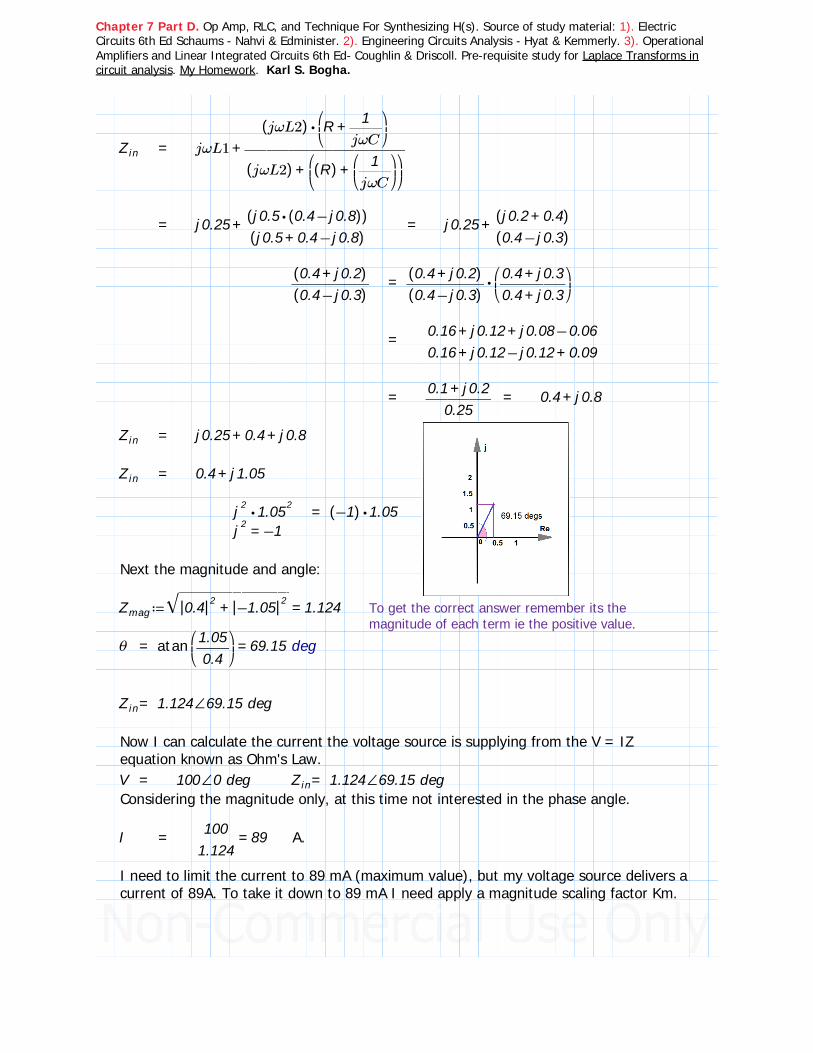
Chapter 7 Part D. Op Amp, RLC, and Technique For Synthesizing H(s). Source of study material: 1). Electric Circuits 6th Ed Schaums - Nahvi & Edminister. 2). Engineering Circuits Analysis - Hyat & Kemmerly. 3). Operational Amplifiers and Linear Integrated Circuits 6th Ed- Coughlin & Driscoll. Pre-requisite study for Laplace Transforms in circuit analysis. My Homework. Karl S. Bogha.
Zin = +jωL1 ――――――――⋅((jωL2)) ⎛⎜⎝
+R ――1jωC
⎞⎟⎠
+((jωL2)) ⎛⎜⎝
+((R)) ⎛⎜⎝――1jωC
⎞⎟⎠⎞⎟⎠
= +j0.25 ――――――(( ⋅j0.5 (( −0.4 j0.8))))(( −+j0.5 0.4 j0.8))
= +j0.25 ――――(( +j0.2 0.4))(( −0.4 j0.3))
――――(( +0.4 j0.2))(( −0.4 j0.3))
= ⋅――――(( +0.4 j0.2))(( −0.4 j0.3))
⎛⎜⎝――――
+0.4 j0.3+0.4 j0.3
⎞⎟⎠
= ――――――――−++0.16 j0.12 j0.08 0.06+−+0.16 j0.12 j0.12 0.09
= ――――+0.1 j0.2
0.25= +0.4 j0.8
Zin = ++j0.25 0.4 j0.8
Zin = +0.4 j1.05
⋅j2 1.052 = ⋅((−1)) 1.05=j2 −1
Next the magnitude and angle:
≔Zmag =‾‾‾‾‾‾‾‾‾‾‾‾‾+||0.4||2 ||−1.05||2 1.124 To get the correct answer remember its the magnitude of each term ie the positive value.
θ = =atan⎛⎜⎝――1.050.4⎞⎟⎠
69.15 deg
Zin= ∠1.124 69.15 deg
Now I can calculate the current the voltage source is supplying from the V = IZ equation known as Ohm's Law. V = ∠100 0 deg Zin= ∠1.124 69.15 degConsidering the magnitude only, at this time not interested in the phase angle.
I = =――100
1.12489 A.
I need to limit the current to 89 mA (maximum value), but my voltage source delivers a current of 89A. To take it down to 89 mA I need apply a magnitude scaling factor Km.

Chapter 7 Part D. Op Amp, RLC, and Technique For Synthesizing H(s). Source of study material: 1). Electric Circuits 6th Ed Schaums - Nahvi & Edminister. 2). Engineering Circuits Analysis - Hyat & Kemmerly. 3). Operational Amplifiers and Linear Integrated Circuits 6th Ed- Coughlin & Driscoll. Pre-requisite study for Laplace Transforms in circuit analysis. My Homework. Karl S. Bogha.
To go from 89 to 89 mA the scaling factor has to be:
Km = =―――89
⋅89 10−31000 NOT the opposite ---> Km = =―――
⋅89 10−3
890.001
Why? To decrease the current I need to increase the impedance/resistance of the components, that is why Km = 1000.
Km = 1000 Answer.
Now the new element values will be:
Rnew = =⋅1000 0.4 400 Ohm Answer.
L1new = =⋅⋅1000 50 10−6 0.05 = 50 mH Answer. ZL = jωL : Ls
L2new = =⋅⋅1000 100 10−6 0.1 = 100 mH Answer.
Cnew = =――――⋅250 10−6
1030.00000025 = 0.250 uF Answer. ZC = ――1
jωC: ――1
Cs
Capacitor C the scaling factor is divided. Check with local Engineer/Lecturer.
Problem 8.20 (Magnitude scaling):
Refer to the circuit below. Obtain H(s) = Vo/Vi for s = j4 x 10^6 rad/s.Scale the network with Km = 10^-3 and compare H(s) for the two networks before and after scaling.
Solution:
s = +0 ⋅j4 106
jω = ⋅j4 106 Therefore ω = ⋅4 106

Chapter 7 Part D. Op Amp, RLC, and Technique For Synthesizing H(s). Source of study material: 1). Electric Circuits 6th Ed Schaums - Nahvi & Edminister. 2). Engineering Circuits Analysis - Hyat & Kemmerly. 3). Operational Amplifiers and Linear Integrated Circuits 6th Ed- Coughlin & Driscoll. Pre-requisite study for Laplace Transforms in circuit analysis. My Homework. Karl S. Bogha.
Now I can start solving for component values for the given radian frequency.
ZL = jωL = =⋅⋅⋅4 106 0.5 10−3 2000 = j2000
The circuit with updated values for L
The voltage across the left branch with 2000 ohm and j2000 mH in series is the voltage Vi.
Voltage across the right branch j2000 is the voltage Vo.
The centre resistor 2000 ohm NOT be taken into consideration for the transfer function H(s).
H ((s)) = ――VoVi
= ―――――j2000
+2000 j2000Simplify this term
= ⎛⎜⎝―――――
j2000+2000 j2000
⎞⎟⎠⎛⎜⎝―――――
−2000 j2000−2000 j2000
⎞⎟⎠
= ―――――――――――+⋅j4 106 ⋅4 106
++−⋅4 106 ⋅j4 106 ⋅j4 106 ⋅4 106
――VoVi
= ―――――+⋅j4 106 ⋅4 106
⋅8 106= +j0.5 0.5 Convert to polar.
=‾‾‾‾‾‾‾‾‾‾‾+||0.5||2 ||0.5||2 0.7071 = ――1
‾‾2=atan⎛⎜⎝
――0.50.5⎞⎟⎠
45 degH ((s)) = ――
VoVi
= ――1
‾‾245 deg Answer.
Next apply magnitude scaling to the components and then calculate the transfer function.

Chapter 7 Part D. Op Amp, RLC, and Technique For Synthesizing H(s). Source of study material: 1). Electric Circuits 6th Ed Schaums - Nahvi & Edminister. 2). Engineering Circuits Analysis - Hyat & Kemmerly. 3). Operational Amplifiers and Linear Integrated Circuits 6th Ed- Coughlin & Driscoll. Pre-requisite study for Laplace Transforms in circuit analysis. My Homework. Karl S. Bogha.
≔Km 10−3
Rnew = =⋅2000 Km 2
Lnew = =⋅⋅j 2000 Km 2j
H ((s)) = ――VoVi
= ――j2+2 j2
Simplify this term
= ⎛⎜⎝――
j2+2 j2⎞⎟⎠⎛⎜⎝――−2 j2−2 j2⎞⎟⎠
= ―――――+j4 4
++−4 j4 j4 4
――VoVi
= ――+j4 48
= +j0.5 0.5 Convert to polar.
=‾‾‾‾‾‾‾‾‾‾‾+||0.5||2 ||0.5||2 0.7071 = ――1
‾‾2=atan⎛⎜⎝
――0.50.5⎞⎟⎠
45 deg
H ((s)) = ――VoVi
= ――1
‾‾245 deg Answer.
The transfer function is the same before and after the application of the magnitude scaling factor. The transfer function is unchanged.
Engineers: In general, any dimensionless transfer function is unaffected by magnitude scaling. A transfer function having units Ohm is multiplied by Km. A function having units 's' is multiplied by '1/Km' (Schaums).

Chapter 7 Part D. Op Amp, RLC, and Technique For Synthesizing H(s). Source of study material: 1). Electric Circuits 6th Ed Schaums - Nahvi & Edminister. 2). Engineering Circuits Analysis - Hyat & Kemmerly. 3). Operational Amplifiers and Linear Integrated Circuits 6th Ed- Coughlin & Driscoll. Pre-requisite study for Laplace Transforms in circuit analysis. My Homework. Karl S. Bogha.
Problem 8.21 (Frequency Scaling):
A three component series circuit contains R = 5 ohmL = 4 HC = 3.9 mF.Obtain the series resonant frequency in rad/s,and then frequency scale the circuit with Kf = 1000.
Solution:
Its an RLC circuit, or for that reason an RL or RC circuit, I start with determning the angular frequency w:Frequency scaling does not apply the same multiplication like in Magnitude scaling, see notes.
≔R 5 Ohm ≔L 4 H ≔C ⋅3.91 10−3 F
≔ω0 =―――1
‾‾‾‾⋅L C8 rad/s
≔Kf 1000
≔Lnew =―L
Kf0.004 H Frequency scaling L/Km see notes.
≔Cnew =―CKf
⋅3.91 10−6 F
≔ω0_new =⋅Kf 8 8000 rad/s
The resistance R was experiencing w0 = 8 rad/s before scaling, since as its value is not frequency dependent. Impedance does not change for the resistor.However, it remains in the circuit working in 8000 rad/s angular frequency.
≔Z ⎛⎝ω0⎞⎠ =R 5 Ohm
≔Z ⎛⎝Kmω0⎞⎠ =R 5 Ohm
End of Solved Example Problems.
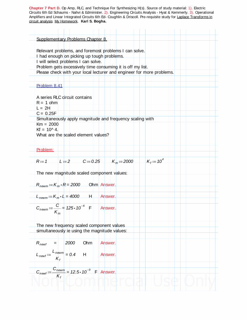
Chapter 7 Part D. Op Amp, RLC, and Technique For Synthesizing H(s). Source of study material: 1). Electric Circuits 6th Ed Schaums - Nahvi & Edminister. 2). Engineering Circuits Analysis - Hyat & Kemmerly. 3). Operational Amplifiers and Linear Integrated Circuits 6th Ed- Coughlin & Driscoll. Pre-requisite study for Laplace Transforms in circuit analysis. My Homework. Karl S. Bogha.
Supplementary Problems Chapter 8.
Relevant problems, and foremost problems I can solve.I had enough on picking up tough problems. I will select problems I can solve.Problem gets excessively time consuming it is off my list. Please check with your local lecturer and engineer for more problems.
Problem 8.41
A series RLC circuit contains R = 1 ohmL = 2HC = 0.25FSimultaneously apply magnitude and frequency scaling withKm = 2000Kf = 10^4.What are the scaled element values?
Problem:
≔R 1 ≔L 2 ≔C 0.25 ≔Km 2000 ≔Kf 104
The new magnitude scaled component values:
≔Rnewm =⋅Km R 2000 Ohm Answer.
≔Lnewm =⋅Km L 4000 H Answer.
≔Cnewm =――C
Km⋅125 10−6 F Answer.
The new frequency scaled component values simultaneously ie using the magnitude values:
Rnewf = 2000 Ohm Answer.
≔Lnewf =――Lnewm
Kf0.4 H Answer.
≔Cnewf =―――Cnewm
Kf⋅12.5 10−9 F Answer.

Chapter 7 Part D. Op Amp, RLC, and Technique For Synthesizing H(s). Source of study material: 1). Electric Circuits 6th Ed Schaums - Nahvi & Edminister. 2). Engineering Circuits Analysis - Hyat & Kemmerly. 3). Operational Amplifiers and Linear Integrated Circuits 6th Ed- Coughlin & Driscoll. Pre-requisite study for Laplace Transforms in circuit analysis. My Homework. Karl S. Bogha.
Problem 8.42
At a frequency w1, a voltage V1 = 25V@0deg V applied to a passive network results in a current I1 = 3.85@-30 deg A.
The network elements are magnitude scaled with Km = 10.
Obtain the current which results from a second voltage source V2 = 10@45deg V,replacing the first, if the second source frequency is w2 = 10^3 w1.
Solution:
≔V1 ∠25 0 deg ≔I1 ∠3.85 −30 deg
≔Z1 =――V1I1
∠6.494 °30 Ohm
Because network elements were magnitude scaled, I need to undo scaling to get the real impedance Z1.
≔Km 10 ≔Z1unscaled =――Z1Km
∠0.649 °30 Ohm
≔V2 ∠10 45 deg V
≔I2 =⎛⎜⎝―――
V2Z1unscaled
⎞⎟⎠
∠15.4 °15 A
2nd circuit need frequency scaling be applied.
ω2 = ⋅103 ω1 ――ω2ω1
= 103 ≔Kf 103

Chapter 7 Part D. Op Amp, RLC, and Technique For Synthesizing H(s). Source of study material: 1). Electric Circuits 6th Ed Schaums - Nahvi & Edminister. 2). Engineering Circuits Analysis - Hyat & Kemmerly. 3). Operational Amplifiers and Linear Integrated Circuits 6th Ed- Coughlin & Driscoll. Pre-requisite study for Laplace Transforms in circuit analysis. My Homework. Karl S. Bogha.
Now the current I2 equal:
≔I2f =―I2Kf
∠0.0154 °15 A My Answer.Schaums answer given was 0.154 @ 15 deg.I said that must/may be a typo error at Schaums.I tried a few ways kept getting the same answer.Youre most welcome to check with your local lecturer/engineer.
Problem 8.43 (Higher Order Active Circuits):
In the circuit below let R1C1 = R2C2 = 10^-3 s.Find v2 for t>0 if a). v1 = cos(1000 t) u(t)b). v1 = sin(1000 t) u(t)
This circuit below is the exact same circuit in this section Example 8.13.
Solution:
From example 8.13:
H ((s)) = ―――――――+1 R1C1s
(( +1 R1C1s)) ((R1C1s))= ―――――――
(( +1 R1C1s))(( +1 R1C1s)) ((R1C1s))
= ―――1
R1C1s
H ((s)) = ――V2V1
= ―――1
R1C1sIn the s (frequency domain).
See notes the example continues to this expression.
v2 = −――1
RC⌠⌡ dv1 t

Chapter 7 Part D. Op Amp, RLC, and Technique For Synthesizing H(s). Source of study material: 1). Electric Circuits 6th Ed Schaums - Nahvi & Edminister. 2). Engineering Circuits Analysis - Hyat & Kemmerly. 3). Operational Amplifiers and Linear Integrated Circuits 6th Ed- Coughlin & Driscoll. Pre-requisite study for Laplace Transforms in circuit analysis. My Homework. Karl S. Bogha.
v2 = ――1
RCs⌠⌡ dv1 t Concludes to this expression for
the answer in example 8.13.Expression in the time domain.
Substitute the component values or terms :
v2 = ――1
10−3⌠⌡ d0
t
⋅cos ((1000 t)) u ((t)) t The value of u(t) becomes 1 when taken from 0 to t.
v2 = ――1
10−3⌠⌡ d0
t
cos ((1000 t)) t
v2 = ⋅⋅――1
1000――
1
10−3sin ((1000 t))
v2 = ⋅⋅――1
10001000 sin ((1000 t))
v2 = sin ((1000 t)) Now if I were to place the u(t) back in the expression it would inform the student/engineer that this expression comes ON for t>0. correct. That is why its in the textbooks and Schaums solution.
v2 = ⋅sin ((1000 t)) u ((t)) Answer.
Similalry for (b) next.
v2 = ――1
10−3⌠⌡ d0
t
⋅sin ((1000 t)) u ((t)) t
Discussion: Situation comes up for v1 = sin(1000t) when t=0, sin (0) = 0. Since, u(t) requires that at t=0 and t>0 the circuit response is ON. So could turning this expression into another expression help smooth out this difficulty? I may or may not have missed this discusson in previous relevant notes.
I tried looking for a trignometry expression that would satisfy my discussion, but could not find one. There was the power relation but it required taking the square root of the expression.
sin2 ((t)) = ⋅―12
(( −1 cos ((2 t)))) <---Thats messy.
I came up with another idea.

Chapter 7 Part D. Op Amp, RLC, and Technique For Synthesizing H(s). Source of study material: 1). Electric Circuits 6th Ed Schaums - Nahvi & Edminister. 2). Engineering Circuits Analysis - Hyat & Kemmerly. 3). Operational Amplifiers and Linear Integrated Circuits 6th Ed- Coughlin & Driscoll. Pre-requisite study for Laplace Transforms in circuit analysis. My Homework. Karl S. Bogha.
My Discussion: What if an initial condition was added to this circuit with a dc power supply with a switch that came on at t=0, this would provide a 1 when t =0, sin(0) would equal 0 and add the initial condition it results in 1.
Adding a parallel connection to C2 allows for the dc 1 v connection to provide charge on C2 equal to 1V. This happens when the switch is closed. When the switch is opened at t=0, the circuit is exactly like we had in the problem. However the voltage at v2 will be 1V this is the initial condition. This 1V dies out in time t.
Now on the sin(t) term at t=0 the condition u(t) is satisfied?WRONG!
Why wrong? =sin ((0 deg)) 0 Does NOT meet u(t) condition ON.=sin ((90 deg)) 1 Does meet u(t) condition.
If the switch is opened at t=0 the capacitor C voltage from the 1V dc supply will eventually die out with time. However, the opamp would provide a voltage at the output terminal which will hold for t>0. Problem: But each time the input cycles thru, sin(1000t) would have a zero. Which means that 1V dc supply has to remain in the circuit so that in t>0 condition there is 1V at least available at v2. At time t>>0, C will be open circuit, and with the switch closed the 1V dc supply provides that initial condition. So if I make the switch is close at t=0, the voltage at v2 will be 1V. The capacitor C would see a gradual build up in potential and reach its peak value soon enough based on the circuit current flow value. Now the voltage at v2 will be 1V +
'whatever is contributed thru the opamp'. If the dc supply remains in the circuit, is that a problem interms of not looking exactly component wise to the original circuit?Can be argued, then return to the first proposed circuit with switch opening at t=0.I say its the math side of things and the circuits side of things some compromise be made. I did NOT make up the question and can be making too much of it!

Chapter 7 Part D. Op Amp, RLC, and Technique For Synthesizing H(s). Source of study material: 1). Electric Circuits 6th Ed Schaums - Nahvi & Edminister. 2). Engineering Circuits Analysis - Hyat & Kemmerly. 3). Operational Amplifiers and Linear Integrated Circuits 6th Ed- Coughlin & Driscoll. Pre-requisite study for Laplace Transforms in circuit analysis. My Homework. Karl S. Bogha.
Continuing with my solution with the second circuit with switch closing at t=0.
I adjust my expression:v2 = +1 ――
1
10−3⌠⌡ d0
t
⋅sin ((1000 t)) u ((t)) t
Placing the 1 to the outside of the integral, otherwise on the inside it would become t, and that would be incorrect.
v2 = −1 ⋅⋅⎛⎜⎝――
11000
⎞⎟⎠――
1
10−3cos ((1000 t))
v2 = −1 cos ((1000 t)) My Answer.This is the also the Schaums Answer provided.
Check with your local lecturer or engineer.Comments: The 1 in the expression remains for all values of cosine (1000t).However we are in the time domain not degrees, where sin (90 deg) = 1, so cos(90) = 0. But sin(1000(0)) = sin(0) and that equals 0, which u(t) cannot impact it to become 1 or ON. Period/Cycle Impact: Whether in time sin(1000t) or in sin(degrees) the input would cycle thru a zero. 2 Pi = 360 degs. 2 Pi t is something 1000t. Should battery value equal magnitude of v1? Yes, preferably. Here for now 1 is adequate. If it were 10V just change it to 10. So I hope that was satisfactory for my discussion.Check with your local lecturer or engineer.
I may have put too much into this. Should I have to proof this circuit, it could be built and analysed by an oscilloscope.
You may have your own ideas.
I said its 'Time I circuit it instead of TRIGNOMETRY IT' - Karl Bogha.

Chapter 7 Part D. Op Amp, RLC, and Technique For Synthesizing H(s). Source of study material: 1). Electric Circuits 6th Ed Schaums - Nahvi & Edminister. 2). Engineering Circuits Analysis - Hyat & Kemmerly. 3). Operational Amplifiers and Linear Integrated Circuits 6th Ed- Coughlin & Driscoll. Pre-requisite study for Laplace Transforms in circuit analysis. My Homework. Karl S. Bogha.
Closing Comments :
I thought of working a few more example problems. I looked through them and figured out the solutions were basically a mix of previous examples. Of course you can pick more problems to solve. The purpose here was to get sufficient understanding of opams to get thru the Hyat and Kemmerly textbook notes of Chapter 13 complex Frequency. That was accomplished in this section. That brought an end to Part 3.
I had thought of a Part 3E for some helpful circuits topic. This was going to be on Frequency Response. However Opamp topic took adequate attention. Its not necessary now since adequate RLC circuits were worked. I suggest going further with Opamp studies and skills. Usually the next topic in circuits would be Frequency Response.
I have completed the prerequisite studies for Laplace Transforms In Circuits Analysis.The objective was to get a working understanding of circuits before applying Laplace Transforms found in Schaums Chapter 16.
Depending on circuits textbook Hyat And Kemmerly has a study on the math side of Laplace Transforms then on the electric circuits.
31 January 2021.K. S. Bogha Dhaliwal.