Chemical Mechanical Planarization - bitsonchips · Chemical Mechanical Planarization Dr Wang...
7
SIMTech Technical Report (PT/01/003/JT) Chemical Mechanical Planarization Dr Wang Zhengfeng Dr Yin Ling Ng Sum Huan Teo Phaik Luan (Joining Technology Group, Process Technology Division, 2001)
Transcript of Chemical Mechanical Planarization - bitsonchips · Chemical Mechanical Planarization Dr Wang...
SIMTech Technical Report (PT/01/003/JT)
Chemical Mechanical Planarization
Dr Wang Zhengfeng Dr Yin Ling
Ng Sum Huan Teo Phaik Luan
(Joining Technology Group, Process Technology Division, 2001)

Chemical Mechanical Planarization PT/01/003/JT
Keywords: Chemical mechanical planarization (CMP); Copper damascenes process; Semiconductor industry; Metrology; Microelectromechanical system (MEMS)
1
1 BACKGROUND Chemical Mechanical Planarization (CMP) is a process that can remove topography from silicon oxide, metal and polysilicon surfaces. It is the preferred planarization step utilized in deep sub-micron IC manufacturing. More recent scaling of transistor critical dimension has required the use of CMP for applications such as shallow trench isolation (STI) and trenched metal interconnection (Cu damascene). CMP has also been utilized for fabrication and assembly of Micro Electro-Mechanical System (MEMS). In principle, CMP is a process of smoothing and planing surfaces with the combination of chemical and mechanical forces. It can, in a way, be thought of as a hybrid of chemical etching and free abrasive polishing. Mechanical grinding alone may theoretically achieve planarization but the surface damage is high as compared to CMP. Chemistry alone, on the other hand, cannot attain planarization because most chemical reactions are isotropic. However, the removal and planarization mechanism is much more complicated than just considering chemical and mechanical effects separately. CMP makes use of the fact that high points on the wafer would be subjected to higher pressures from the pad as compared to lower points, hence, enhancing the removal rates there and achieving planarization.[1]
CMP is most widely utilized in back-end IC manufacturing. In these process technology and steps thin layers of metal and dielectric materials are used in the formation of the electrical interconnections between the active components of a circuit (e.g. transistors, as formed in the front-end processing). As shown in figure 1, the interconnect is manufactured by depositing thin films of materials, and selectively removing or changing the properties of these materials in certain areas. A new level of thin film is deposited on top of old films and the process is repeated many times until the interconnect is complete. The goal of the CMP process is to planarize step heights caused by the deposition of thin films over existing non-planar features, so that further levels may be added onto a flat surface.[2]
Damascene process, as well as its upgraded generation – dual-damascene, is the critical technology in the transition from aluminum to copper interconnects in semiconductor manufacturing.[3] There are two primary factors driving this transition: the lower resistivity and the increased electromigration resistance that copper offers relative to aluminum. Several new materials and processes are required in this change. In the copper interconnect fabrication process, a simpler dielectric etching replaces metal-etch as the critical step that defines the width spacing of the interconnect lines, while the burden of planarization shifts to the metal deposition and CMP steps.
Figure 1 Cross-section diagram of internal dielectric on top of metal line before and after CMP (the left and the middle charts) and application of Metal 2 and ILD 2 (the right chart)

Chemical Mechanical Planarization PT/01/003/JT
2
During the CMP of patterned copper wafers, two phenomena – copper dishing and SiO2 erosion – lead to deviations from the ideal case depicted in figure 2(a). Copper dishing and SiO2 erosion occur during the over-polish step (which is required to ensure complete copper removal across the entire wafer) and are defined schematically in figure 2(b).[2]
Copper dishing is defined as the difference in height between the center of the copper line – i.e. the lowest point of the dish – and the point where the SiO2 levels off – i.e. the highest point of the SiO2. Copper dishing occurs because the polishing pad bends slightly into the recess to remove copper from within the recess. The SiO2 erosion is a thinning of the SiO2 layer resulting from the non-zero polish rate of SiO2 during over-polish step. The SiO2 erosion is defined as the difference in the SiO2 thickness before and after the polish step. Both copper dishing and SiO2 erosion are undesirable because they reduce the final thickness of the copper line; and copper dishing leads to non-planarity of the surface resulting in
complications when adding multiple levels of metal. CMP is also readily adaptable as an enabling technology in Micro-electro-mechanical Systems (MEMS) fabrication, particularly polysilicon surface micromachining.[4] CMP not only eases the design and manufacturability of MEMS devices by eliminating several photolithographic and film issues generated by severe topography, but also enables far greater flexibility with process complexity and associated designs. Thus, the CMP planarization technique alleviates processing problems associated with fabrication of multi-level polysilicon structures, eliminates design constraints linked with non-planar topography, and provides an avenue for integrating different process technologies. Examples of these enhancements include the extension of surface micromachining fabrication to multiple mechanical layers, as illustrated in figure 3, the monolithic integration of electronics and MEMS, and the combination of bulk and surface micromachining.
DishingErosion
SiO2
Cu
Figure 2 Left chart: (a) Schematic representation of copper dishing and SiO2 erosion; Right chart: (b) Profilometer trace of a 100µm line exhibiting 305nm of dishing
Figure 3 Two SEM images show the surface of polysilicon before and after CMP polishing and the result of profilometer measurement
Chemical Mechanical Planarization PT/01/003/JT
3
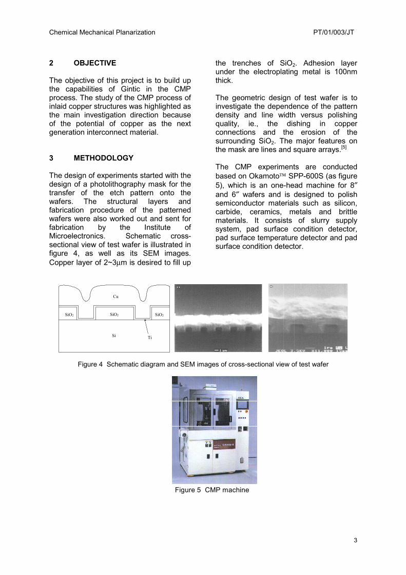
2 OBJECTIVE The objective of this project is to build up the capabilities of Gintic in the CMP process. The study of the CMP process of inlaid copper structures was highlighted as the main investigation direction because of the potential of copper as the next generation interconnect material. 3 METHODOLOGY The design of experiments started with the design of a photolithography mask for the transfer of the etch pattern onto the wafers. The structural layers and fabrication procedure of the patterned wafers were also worked out and sent for fabrication by the Institute of Microelectronics. Schematic cross-sectional view of test wafer is illustrated in figure 4, as well as its SEM images. Copper layer of 2~3µm is desired to fill up
the trenches of SiO2. Adhesion layer under the electroplating metal is 100nm thick. The geometric design of test wafer is to investigate the dependence of the pattern density and line width versus polishing quality, ie., the dishing in copper connections and the erosion of the surrounding SiO2. The major features on the mask are lines and square arrays.[5] The CMP experiments are conducted based on Okamoto SPP-600S (as figure 5), which is an one-head machine for 8″ and 6″ wafers and is designed to polish semiconductor materials such as silicon, carbide, ceramics, metals and brittle materials. It consists of slurry supply system, pad surface condition detector, pad surface temperature detector and pad surface condition detector.
SiO2
Ti
Cu
Si
SiO2 SiO2
Figure 4 Schematic diagram and SEM images of cross-sectional view of test wafer
Figure 5 CMP machine

Chemical Mechanical Planarization PT/01/003/JT
4
A 2-Phase process is adopted in our inlaid copper pattern wafer polishing, which means changing slurry and working conditions during the copper removal process. The goal of the 1st Phase CMP is to remove copper layer with high efficiency. This phase stops at the surface of the barrier layer. Then changing the slurry and machine status to 2nd Phase for the remaining copper and barrier with removal rate at 1:1 selectivity. The most significant benefit brought by a 2-Phase process is to eliminate the excessive dishing caused by oxidants that is used for high copper removal rate. At the 2nd Phase, lower Cu/barrier selectivity slurry minimizes dishing on patterned structures as well. In order to find out the average efficiency of the 1st Phase removal sequence, the thickness of the copper layer is measured after each fixed process time. CMP polishing has been performed on the patterned wafers under different head load and speed in order to characterize the polishing quality and process parameters. The surface profiles before and after CMP are fetched through profilometer and atomic force microscopy (AFM) measurement. Some CMP investigations related to the process are also conducted,
e.g. polishing pad wearing and SiO2 polishing. Gold bump planarization was conducted to explore the application of CMP into electronic packaging. The purpose is to polish the top surface of gold bumps on the silicon wafer and therefore, reduce the surface roughness of bumps in order to enhance the wafer-bumping reliability. The experiment was conducted on a 6″ wafer with arrays of gold bump, which was electroplated on passivation layer for protection of underlying IC. 4 RESULTS A database has been established that consists of information on the dependence among CMP process parameters, geometrical characteristic of test wafer and polishing qualities on wafer surface. Figure 6 shows the relations between dishing (copper) & erosion (silicon oxide) and pattern characters (pattern density and linewidth). The data are collected from the same wafer and measured by profilometer (>10µm lines) and AFM (<10µm lines) due to the limited scanning scope of AFM (100µm in this case).
-100
-50
0
50
100
150
200
250
0 20 40 60 80 100 120
Linewidth (mm)
Dis
hing
(nm
)
20%40%50%80%
No. 208.1.16L150S50
-100
-50
0
50
100
150
200
250
0 20 40 60 80 100
Pattern density (%)
Dis
hing
(nm
) 100 microns50 microns10 microns5 microns2 microns
0
100
200
300
400
500
600
0 20 40 60 80 100 120
Linewidth (mm)
Eros
ion
(nm
)
20%
40%
50%
80%
No. 208.1.16L150S50
0
100
200
300
400
500
600
0 20 40 60 80 100
Pattern density (%)
Eros
ion
(nm
) 100 microns50 microns10 microns 5 microns
No. 208.1.16L150S50
Figure 6 Pattern characters (pattern density & linewidth) versus dishing (Cu) & erosion (SiO2).
200g/cm2 of head load and 50rpm of spindle/carrier speed is set for 2nd Phase polishing

Chemical Mechanical Planarization PT/01/003/JT
5
By changing the process parameters (head load and spindle/carrier speed), a variety of experiments are conducted and from which, measurements have been taken. By and large, some trends about the relations between process conditions and surface finishing could be extracted as below: • The severest over-polishing of copper
material (dishing effect) normally emerges when the head pressure is about 150g/cm2 within our experimental scope.
• The dishing depth of copper layer
keeps pretty consistent along with the changing of machine speed, while relatively serious over-polishing of copper could be expected when the speed is around 75rpm.
• No obvious trend has been found
between the erosion depth of the dielectric layer with the head pressure within our probed process range.
• The most serious over-polishing effect
of silicon oxide layer often occurs when the machine speed is around 75rpm.
By analyzing the polishing results from AFM measurement towards copper lines with <10µm width, a common cross-sectional profile, as shown in figure 7, is acquired. From a macro view, over-polishing of copper (dishing) always occurred as illustrated in figure 2, as all the profilometer measurement shows. On the other hand, when lines go to less than 10µm wide, extruding copper lines above the dielectric layer are dominating the situation. One possible explanation for this anomaly is galvanic corrosion between the thin layer of titanium and the copper features. The galvanic corrosion attack occurs from the point when the titanium is first exposed and continues until all the titanium is being removed. It can be said that dishing is occurring in the titanium layer rather than the copper layer. Gold bump polishing is carried out under typical process conditions. The results indicated in figure 8 show the before and after CMP images on bump surface, which roughness was reduced from 216.00nm to 93.95nm before and after 5 minutes of polishing.
Figure 7 3-D AFM image and section analysis of 2µm copper lines with pattern density of 50%
Before CMP
After CMP
BeforeCMP
AfterCMP
Figure 8 The images of gold bump surface before and after CMP. The two images by the left were
taken from Veeco laser interferometer and the two by the right from AFM

Chemical Mechanical Planarization PT/01/003/JT
6
Within-wafer uniformity of copper polishing is read out as well by taking comparison of dishing heights on copper lines of different dies within the same wafer. An encouraging uniformity of <10% deviation has been acquired in this test. 5 CONCLUSIONS A variety of CMP experiments of metallic and nonmetallic materials have been conducted. By highlighting on the patterned copper polishing, some trends have been extracted to describe the relations between CMP process conditions and the surface finishing. The promising results on gold bump polishing indicated that the CMP might find its position in electronics packaging applications. 6 INDUSTRY SIGNIFICANCE CMP plays significant roles in today and tomorrow’s semiconductor industry, especially in forming the copper interconnection on silicon wafers. Since the nonstop trend of miniature in device features makes the conventional interconnection technology insufficient to cope with the tremendous pattern density and small line width, copper has been put front as the ideal replacement of conduct material. CMP is the key step to pattern the copper interconnection layer, instead of the conventional etching process that does not work on copper material. During our project the two crucial defects of copper CMP technology, dishing of copper and over-polish of dielectric, have been investigated. Relevant collaborative researches can be conducted with local and international semiconductor factories, CMP equipment producers and also the consumable (slurry and polishing pad) manufacturers. The possible collaboration fields could be process study on copper polishing and dielectric isolation, consumable development, etc.
More potential applications of CMP can be expected in the field of microelectronics packaging due to the outstanding characteristics of CMP process on surface planarization of various materials and substrates. Micro-Electro-Mechanical System (MEMS) is an emerging technology that has large potential market value. Apart from the great success in automotive industry by integrating micro sensors with airbag system, Opto-MEMS and Bio-MEMS will be the next two possible areas of large commercial potential for MEMS to explore. CMP can be the ideal tool of surface polishing in the Opto-MEMS and Bio-MEMS packaging, assembly and even fabrication. Along with the growing of MEMS industry, extensive applications of CMP could be explored in these fields. REFERENCES 1. Joseph M. Steigerwald, Shyam P. Murarka
and Ronald J. Gurmann, Chemical Mechanical Planarization of Microelectronic Material, John Wiley & Sons, Inc., 1997
2. Taber Hardesty Smith, Device Independent Process Control of Dielectric Chemical Mechanical Polishing, MIT Ph.D. dissertation, September 1999
3. M.E. Gross, C. Lingk, W.L. Brown, R. Drese, “Implications of damascene topography for electroplated copper interconnects,” Solid State Technology, pp. 47-52, August 1999
4. Jeffry J. Sniegowski, “Chemical-Mechanical Polishing: Enhancing the Manufacturability of MEMS”, pp.104-115, SPIE Vol. 2879, 1996.
5. MIT/SEMATECH 931AZ Copper (Cu) Chemical Mechanical Planarization Test Chip Design, Layout, and Electrical Test, Technology Transfer #98103580A-TR, SEMATECH, November 1998.